Loading ...
Loading ...
Loading ...
13
Pin layout
2.4 Pin layout
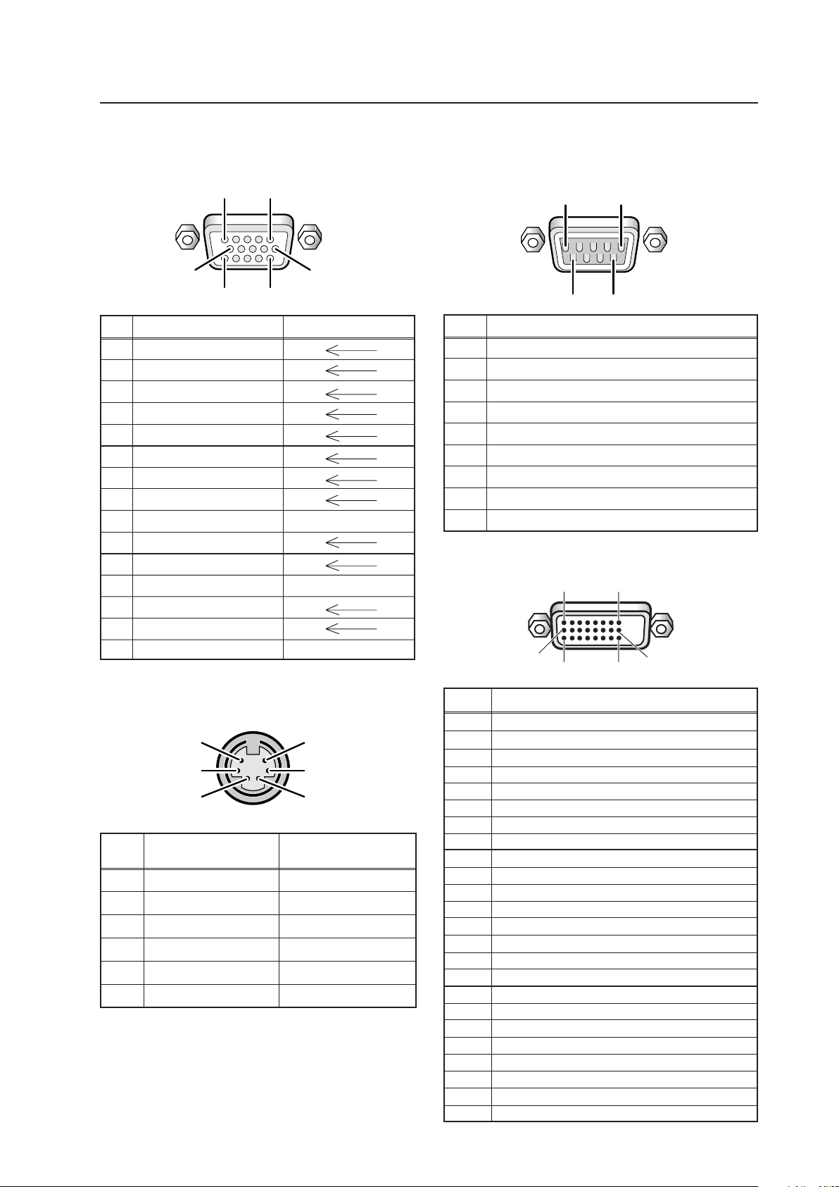
INPUT1 (Mini D-sub, 15-pin connector; female)
pin layout
Pin No.
Signal
1 NC (not connected)
2 TxD (Transmit Data)
3 RxD (Receive Data)
4 NC (not connected)
5 GND
6 NC (not connected)
7 NC (not connected)
8 RTS (Request To Send)
9 NC (not connected)
Pin No.
Combination Combination
IN OUT
1 GND GND
2 NC (not connected) NC (not connected)
3 TxD (output) RxD (input)
4 NC (not connected) NC (not connected)
5 RxD (input) TxD (output)
6 NC (not connected) NC (not connected)
Combination IN/OUT terminal pin layout
5
3
1
6
4
2
RS-232C terminal (D-sub 9-pin connector; male)
pin layout (DCE format)
Pin No.
Input Output
1 R
2 G
3 B
4 NC (not connected)
5 GND
6 GND
7 GND
8 GND
9 DDC +5V NC (not connected)
10 GND
11 NC (not connected)
12 DDC SDA NC (not connected)
13 HD or H/V SYNC
14 VD
15 DDC SCL NC (not connected)
INPUT2 (DVI-D 24 pin connector; female)
pin layout
Signal Assignment
1
2
3
4
5
6
7
8
9
10
11
12
13
14
15
16
17
18
19
20
21
22
23
24
T.M.D.S. Data2–
T.M.D.S. Data2+
T.M.D.S. Data2/4 Shield
NC (No connection)
NC (No connection)
DDC Clock
DDC Data
NC (No connection)
T.M.D.S. Data1–
T.M.D.S. Data1+
T.M.D.S. Data1/3 Shield
NC (No connection)
NC (No connection)
+5V Power
GND
Hot Plug Detect
T.M.D.S. Data0 –
T.M.D.S. Data0+
T.M.D.S. Data0/5 Shield
NC (No connection)
NC (No connection)
T.M.D.S. Clock Shield
T.M.D.S. Clock+
T.M.D.S. Clock–
Pin No.
1 2
16
2417
9
5
96
1
1
6
1115
5
10
Loading ...
Loading ...
Loading ...