
LN882H-CBU Module Specification
Document version:20240514

catalogue
Catalogue
1 Product Overview 2
1.1 characteristic .....................................................................................................................................
2
1.2 application area .................................................................................................................................
2
1.3 Update Note .....................................................................................................................................
3
2 Module Interface 4
2.1 Dimension Packaging .................................................................................................................... 4
2.2 Pin Definition ................................................................................................................................. 4
3 Electrical Parameters 7
3.1 Absolute Electrical Parameters ....................................................................................................
7
3.2 normal running conditions ............................................................................................................
7
3.3 Radio frequency power consumption ............................................................................................
7
3.4 Working Current .............................................................................................................................
8
4 Radio Frequency Parameters 9
4.1 Basic Radio Frequency Characteristics .......................................................................................
9
4.2 Wi-Fi transmission performance ....................................................................................................
9
4.3 Wi-Fi reception performance ........................................................................................................ 10
4.4 Bluetooth transmission performance ....................................................................................... 10
4.5 Bluetooth reception performance ................................................................................................ 10
5 Antenna Information 12
5.1 Antenna type .................................................................................................................................. 12
5 .2 Reduce antenna interference ........................................................................................................ 12
6 Packaging Information and Production Guidelines 13
6.1 Mechanical Dimension ................................................................................................................ 13
6.2 Recommended WL2H-U package ................................................................................................ 16
6.3 Production Guide ......................................................................................................................... 17
6.4 Recommended furnace temperature curve ............................................................................... 18

catalogue
1
/
20
LN882H-CBU is a low-power embedded Wi-Fi module. It consists of a highly integrated wireless
RF chip LN882 H and a few peripheral components, supporting both AP and STA dual-role connections,
as well as low-power Bluetooth connectivity.

1 Product Overview
2
/
20
1 Product Overview
LN882H-CBU features an 32-bit MCU with an internal operating frequency up to 160 MHz,
along with 128 KB ROM and 296 KB RAM. The MCU is specifically designed with signal
processing extension instructions, enabling efficient audio encoding and decoding. It offers a rich array of
peripherals, including PWM,UART, and SPI. Up to five 32-bit PWM outputs make the chip highly
suitable for high-quality LED control.
1.1 Characteristic
• Built-in low-power 32-bit CPU that also serves as an application processor
• The clock frequency supports 160 MHz
• Operating voltage:3.0V~3.6V
• Peripherals:5×PWM, 2×UART, 1×SPI
• Wi-Fi Connectivity
– 802.11 b/g/n
– Channel 1-14@2.4GHz
– Supports WEP, WPA/WPA2, WPA/WPA2 PSK (AES), and WPA3 security modes
– Maximum output power of +18 dBm under the 802.11b mode
– Supports STA/AP/STA+AP operating modes
– Supports both SmartCon and AP distribution network configurations(including Android and
iOS devices)
– Board-mounted PCB antenna
– Operating temperature: -40°C to 105°C
– Board-mounted PCB
• Bluetooth Connectivity
– Bluetooth mode supports a transmission power of 1 dBm
– Complete Bluetooth coexistence interface
antenna
1.2 Application Area
• Smart Building
• Smart Home/Home Appliances
• Smart socket, smart light
• Industrial Wireless Control
• Infant surveillance camera

1 Product Overview
3
/
20
• web camera
• Intelligent Public Transport
1.3 Update Note
Date updated
Update Content
Updated version
V1.0.0
New document
2024-05-14
2 Module Interface
4
/
20
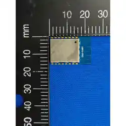
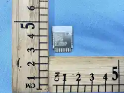
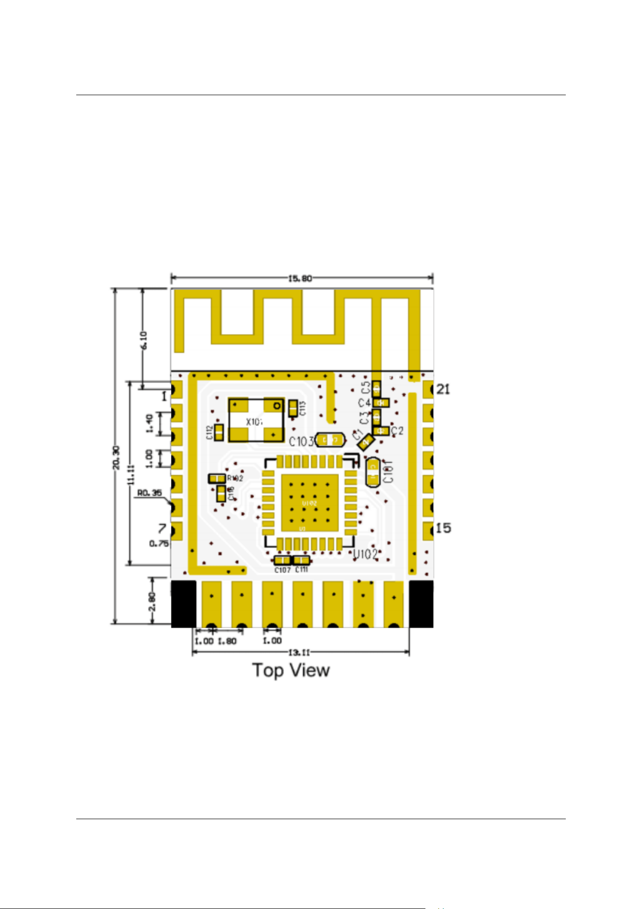
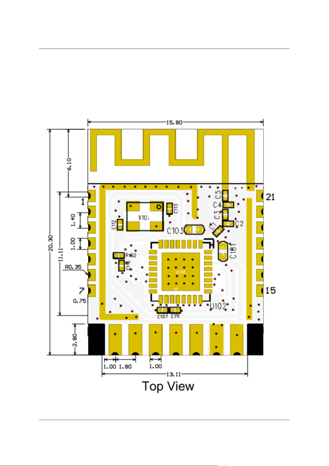
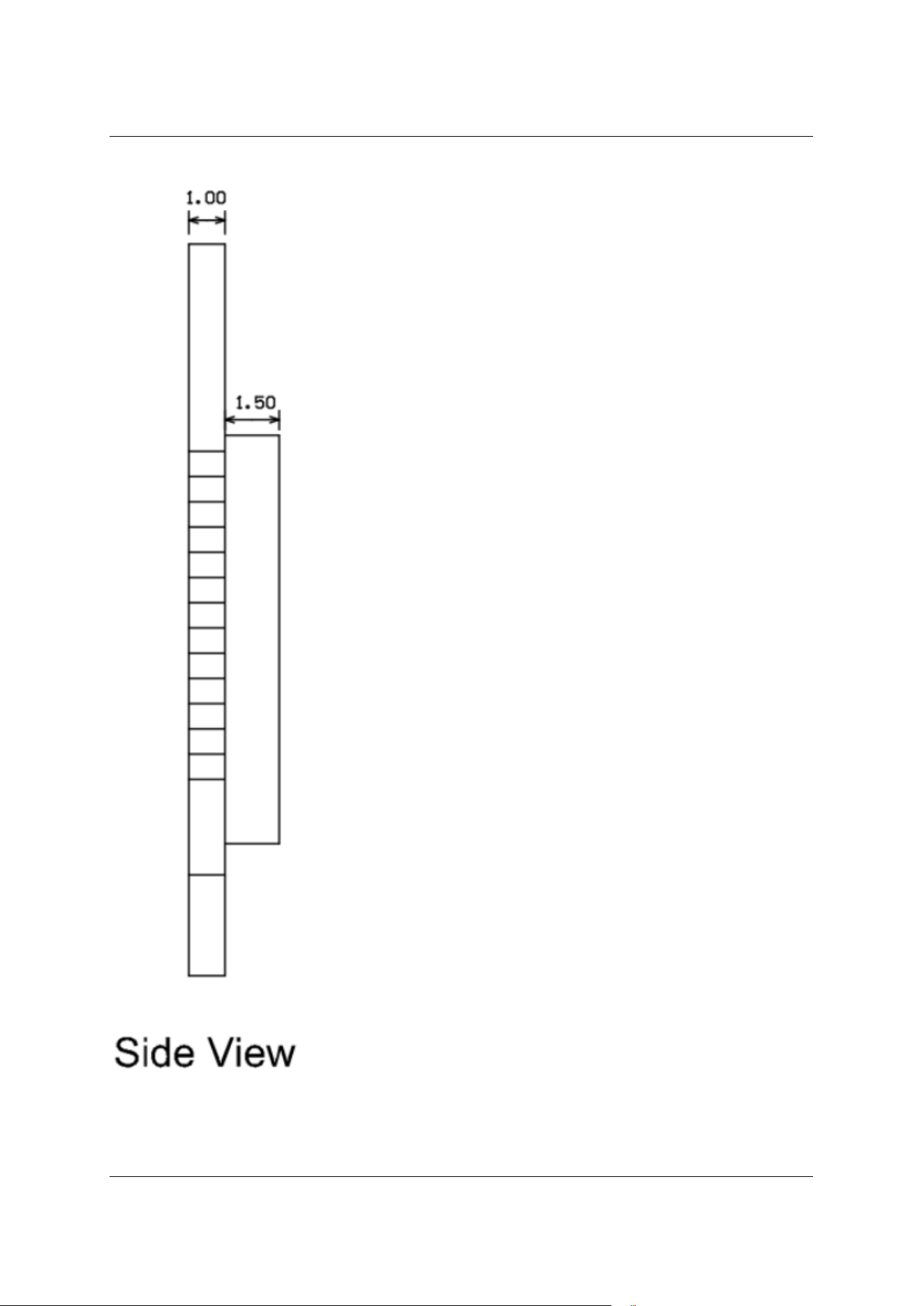
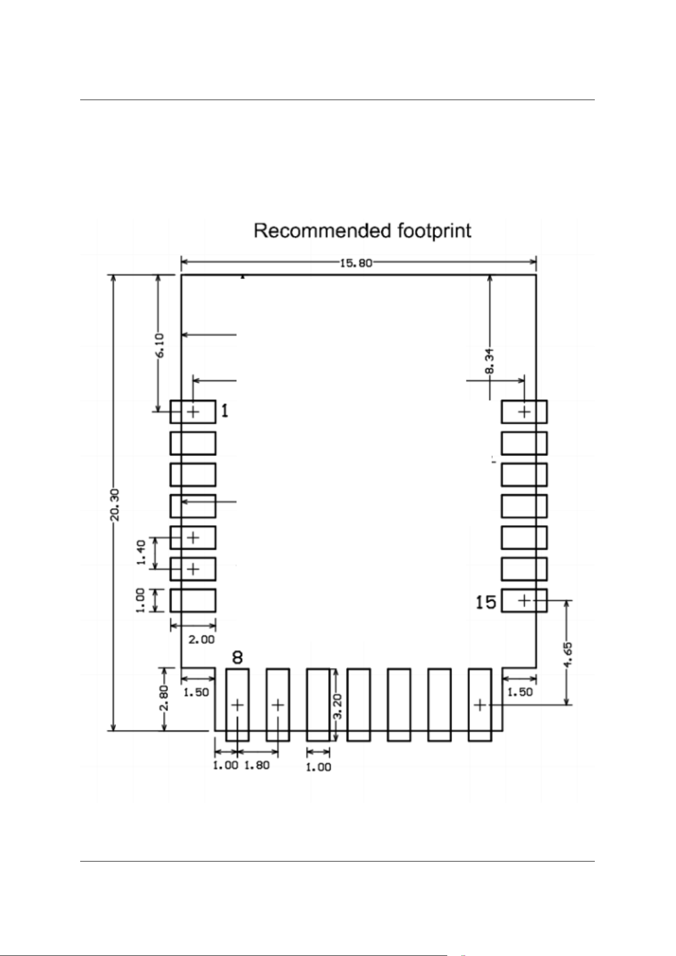
2 Module Interface
2.1 Dimension Packaging
LN882H-CBU dimensions: 15.8±0.35mm (W) × 20.3±0.35mm (L) × 2.5±0. 15mm
(H).The dimensions are shown below:
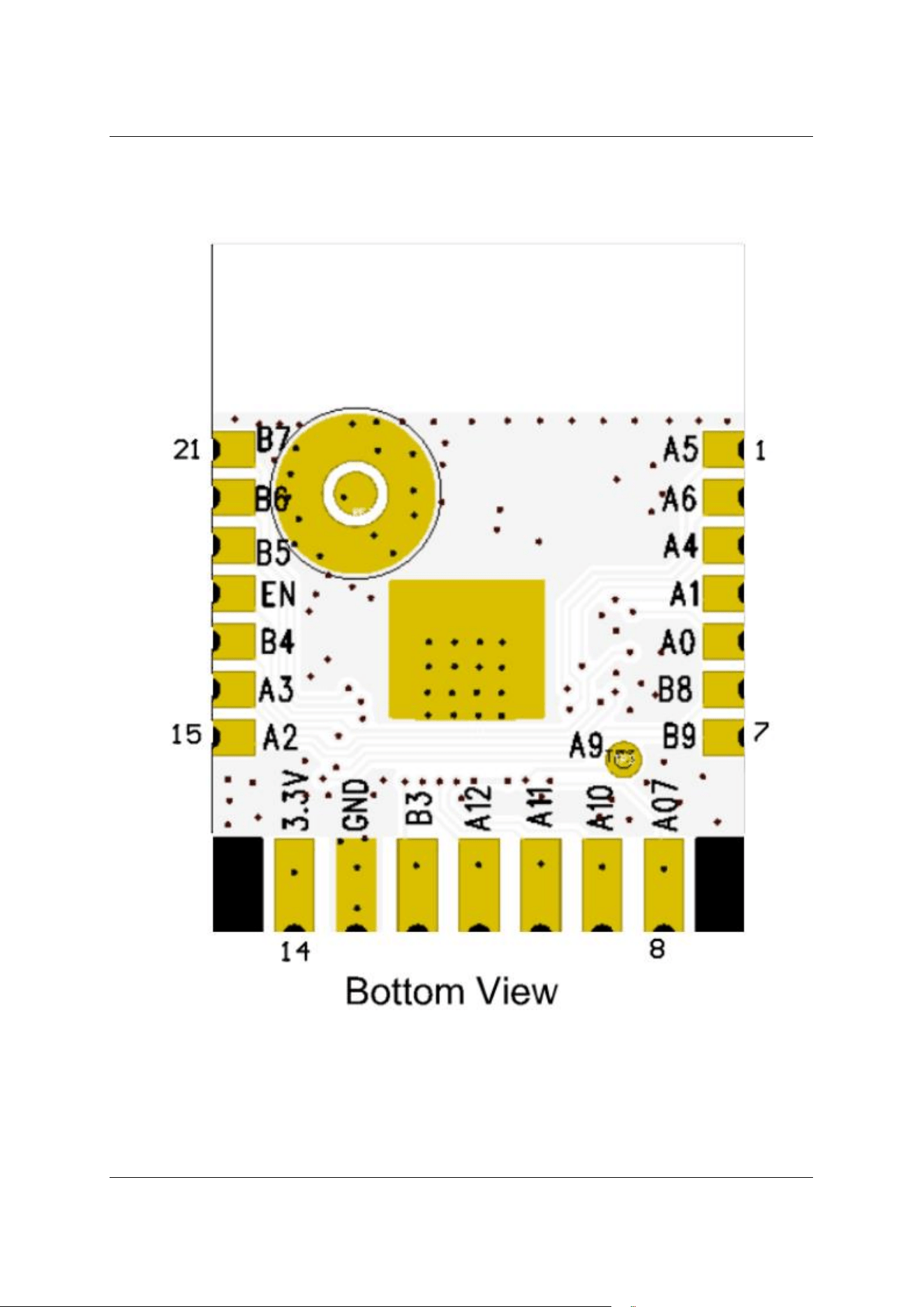
2.2 Pin Definition

2 Module Interface
5
/
20
Pin number
Symbol
IO Type
Function
1
GPIOA5
I/O
The regular GPIO can be
reused as SPI_SCK(corr-
esponding to Pin 13 of the
IC)
2
GPIOA6
I/O
The regular GPIO can be
reused as SPI_MOSI(corr-
esponding to Pin 14 of the
IC)
3
GPIOA4
I/O
Ordinary GPIO (corre-
sponding to IC's Pin 12)
4
GPIOA1
I/O
Ordinary GPIO (corre-
sponding to IC's Pin 9)
5
GPIOA0
I/O
ADC port,corresponding
to IC's GPIOA0 (corre-
sponding to IC' s Pin 8)
6
GPIOB8
I/O
UART_RX1 ,corresponds
to IC's GPIOB8 (corre-
sponds to IC' s Pin 29)
7
GPIOB9
I/O
UART_TX1 ,print log
port,corresponding to
IC's GPIOB9 (corres-
ponding to IC' s Pin 30)
8
GPIOA7
I/O
Supports hardware P WM(cor-
responding to IC's Pin 15)
9
GPIOA10
I/O
Supports hardware P WM(cor-
responding to IC's Pin 21)
10
GPIOA11
I/O
Supports hardware P WM(cor-
responding to IC's Pin 22)
11
GPIOA12
I/O
Supports hardware P WM(cor-
responding to IC's Pin 23)
12
GPIOB3
I/O
Supports hardware P WM(cor-
responding to IC's Pin 24)
13
GND
P
Power supply location

2 Module Interface
6
/
20
Pin number
Symbol
IO Type
Function
14
3.3V
P
Power supply 3V3
15
GPIOA2
I/O
UART_TX0, the user
data transmission port,
corresponds to GPIOA2
of IC(corresponding to
Pin 10 of IC)
16
GPIOA3
I/O
UART_RX0, user data
reception port, corres-
ponding to GPIOA3 of
IC(corresponding to Pin
11 of IC)
17
GPIOB4
I/O
Ordinary GPIO,can be
reused as ADC2 (corres-
ponding to IC's Pin 24)
18
EN
I/O
Reduction foot: effective at low
voltage, with internal pull-up
handling, compa tible with other
module designs for integration
19
GPIOB5
I/O
Ordinary GPIO (corre-
sponding to IC's Pin 26)
20
GPIOB6
I/O
The regular GPIO can be
reused as SPI_MISO(corr-
esponding to Pin 27 of the
IC)
21
GPIOB7
I/O
The regular GPIO can be
reused as SPI_CS(corres-
ponding to Pin 28 of IC)
Top surface measurement point
GPIOA9
I/O
Mode selection pin: pull low
before power-up to enter
programming mode (corre-
sponding to IC's Pin 17)
Note:P represents the power pin, and I/O represents the input/output pins.

3 Electrical Parameters
7
/
20
3 Electrical Parameters
3.1 Absolute Electrical Parameters
Parameter Description Least value Crest value Unit
Ts
VBAT
Service voltage
-0.3 3.9 V
Electrostatic release
voltage (human
model)
-4 4 kV
Electrostatic release
voltage (machine
model)
TAMB-25℃ -200 200 V
3.2 Normal Running Conditions
Parameter Description Least value Representative value Crest value Unit
Ta
105
VBAT
Service voltage 3 3.3
3.6 V
VOL
IO low-level
output
VSS
-
VSS+0. 3
VOH
IO High-
level output
VBAT-0.3
-
VBAT V
Imax
IO drive current-
6
20
3.3 Radio frequency power consumption
Operative mode Pattern Speed
Transmission Power
Average Rate/ Reception Value
Peak (typ-
ical value)
Unit
Launch 11b 11Mbps
+18dBm
297 375 mA
Launch 11g 54Mbps 242 355
+18dBm
mA
Launch 11n MCS7
+18dBm 236 353 mA
mA
V
℃
-
Working temper -40
TAMB-25℃
℃ 125 -55
Storage Temperature

3 Electrical Parameters
8
/
20
Operative mode Pattern
Speed
Transmit
power/ rec-
eiving power
Average value
Peak (typ-
ical value)
Unit
Receive 11b 11Mbps Continuous Reception 78 90 mA
Receive 11n MCS7 Continuous Reception 78 90 mA
3.4 Working Current
Work pattern
Working st-
ate,Ta=25°C
Average value
Maximum value (typical value)
Unit
Quick connection ne-
twork status (Bluetooth
network configuration)
The module is in Quick Connect
mode
Network status: The
Wi-Fi indicator light
flashes.
88
288
mA
Fast-link distribution
network status (AP
distribution network)
The module is in a hot
spot distribution network
state, and the Wi-Fi
indicator light is flashing
slowly.
105
370
mA
Fast-link distribution
network status (EZ
distribution network)
The module is in Quick Connect
mode
Network status: The
Wi-Fi indicator light
flashes.
92
354
mA
Network connection status
The module is in netw-
orked operation mode,
and the Wi-Fi indicator
light is always on.
93
222
mA
Poor network connection status
The module and hotspot are located
at
Poor net work conn ection st atus
Wi-Fi indicator
light remains on
100
373
mA
Network connection status
The module is ope-
rating offline. The
Wi-Fi indicator light
remains off.
96
388
mA
Receive 11g 54Mbps Continuous Reception 78 90 mA

9
/
2
4 Radio Frequency Parameters
0
4 Radio Frequency Parameters
4.1 Basic Radio Frequency Characteristics
Parameter Item Define
Service frequency
Wi-Fi standard
IEEE 802. 11b/g/n (Channels 1–14)
Data transmission rate
11g:6、9、12、18、24、36、48、
54(Mbps);
11n:HT20 MCS0~7;
Antenna type
PCB antenna gain 0 dBi
4.2 Wi-Fi Transmission Performance
Parameter Item Least value Representative value Crest value Unit
RF average output power
Rate, 802. 11b
CCK Mode 11
M
-
18
-
dBm
RF average
output power,
802. 11g OFDM
Mode 54M
-
18
-
dBm
RF average output power
Rate,802. 11n
OFDM Mode
MCS7(HT20)
-
18
-
dBm
Frequency error
-20
-
20
ppm
11b:1、2、5.5、11 (Mbps);
2.412~2.462 GHz

4 Radio Frequency Parameters
10
/
20
4.3 Wi-Fi Reception Performance
Parameter Item Least value
Representative value
Crest value Unit
PER<8%, RX se-
nsitivity,802. 11b
DSSS Mode 11M
-
-88
-
dBm
PER<10%, RX
sensitivity,802.11
g OFDM Mode
54M
-
-74
-
dBm
PER <10%, RX
sensitivity
802.11n
OFDM Mode
MCS7(HT20)
-
-72
-
dBm
PER<10%, RX
sensitivity,Blood
1M
-
-90
-
dBm
4.4 Bluetooth Transmission Performance
Parameter Item Least value Representative value Crest value Unit
Air Speed
-
1
-
Mbps
Transmitting power
-20
1
20 dBm
Frequency error
-150
-
150 KHz
4.5 Bluetooth Reception Performance
MHz
2480
-
2402
Service frequency

4 Radio Frequency Parameters
11
/
20
Parameter Item
Least value
Representative value
Crest value
Unit
Maximum RF
signal input
-10
-
-
dBm
Intermodulation
-
-
-23
dBm
Common Channel Suppression Ratio
-
10
-
dB
dBm
-
-90
-
RX sensitivity

5 Antenna Information
12
/
20
5 Antenna Information
5.1 Antenna Type
The LN882H-CBU antenna is an onboard PCB antenna.
5.2 Reduce Antenna Interference
When using a PCB board-mounted antenna on the Wi-Fi module, to ensure optimal Wi-Fi performance, it is
recommended that the distance between the module antenna section and other metal components be at least 15 mm.
Do not trace or even copper-clad the user's PCB board in the antenna area to avoid affecting antenna performance.
6 Packaging Information and Production Guidelines
13/
20
6 Packaging Information and Production Guidelines
6.1 Mechanical Dimension
LN882H-CBU PCB dimensions:15.8±0.35 mm (W) × 20.3±0.35 mm (L) × 1.0±0.1 mm (H).
6 Packaging Information and Production Guidelines
14/
20
6 Packaging Information and Production Guidelines
15/
20
6 Packaging Information and Production Guidelines
16/
20
6.2 LN882H-CBU Recommended Package

6 Packaging Information and Production Guidelines
17/
20
6.3 Production Guide
1. The factory-produced surface-mount and plug-in packaged modules adopt assembly methods selected according to the
customer's substrate design specifications. Substrate designs intended for surface-mount packaging are manufactured using
the SMT surface-mount process, while those designed for plug-in packaging are produced via the wave soldering process.
Upon unpacking, module products should undergo soldering within 24 hours; otherwise, they must be stored in a
desiccator with humidity not exceeding 10</sp_3 <%4>%, RH, or re-vacuum-packed with recorded exposure time,
ensuring total exposure duration does not exceed 168 hours.
•(SMT process) Instruments or equipment required for SMT mounting:
– chip shooter
– SPI
– reflow soldering
– Furnace Temperature Tester
– AOI
• (Bump welding process) Instruments or equipment required for bump welding:
– Wave soldering equipment
– Wave soldering fixture
– Thermostatic soldering iron
– Tin bars, tin wires, flux
– Furnace Temperature Tester
• Instruments or equipment required for baking:
– Cabinet oven
– Anti-static, high-temperature resistant pallet
– Anti-static, high-temperature resistant gloves
2. The storage conditions for the factory-produced modules are as follows:
• The moisture-proof bag must be stored in an environment with temperature <40°C and humidity <90%RH.
• For dried packaged products, the shelf life is 12 months from the date of packaging seal.

6 Packaging Information and Production Guidelines
18/
20
3. Modules leaving the factory should be baked if they are at risk of moisture exposure.
• The vacuum packaging bag was found damaged before opening.
• Upon opening, no humidity indicator card was found inside the packaging bag.
• After opening the package, if the humidity indicator card reads 10% or higher, the color ring turns pink.
• The total exposure time after unsealing exceeds 168 hours
• More than 12 months have passed since the first sealed packaging date
4 . The baking parameters are as follows:
• Baking temperature: Roll packaging 60°C, humidity ≤ 5%RH; Tray packaging 125°C,
humidity ≤ 5%RH(High-temperature resistant trays are not used for plastic-informed boxes).
• Baking time:48 hours for roll packaging;12 hours for tray packaging
• Alarming temperature setting: reel packaging 65°C; pallet packaging 135°C
• After cooling to below 36°C under natural conditions, production can begin.
• If the exposure time after baking exceeds 168 hours, bake again if not fully used.
• If the exposure time exceeds 168 hours without baking, it is not recommended to use reflow or
wave soldering processes for this batch of modules. Since the modules contain Grade 3
humidity-sensitive components that may become damp after exceeding the permitted exposure
time, high-temperature soldering could lead to component failure or poor solder joints.
5. During the entire production process, please provide electrostatic discharge (ESD) protection for the modules.
6. To ensure the product pass rate, it is recommended to use SPI and AOI testing equipment to monitor the quality of solder paste
printing and mounting.
6.4 Recommended Furnace Temperature Curve
Select the appropriate welding method based on the process requirements: refer to the recommended reflow soldering furnace temperature
curve for SMT, and the recommended wave soldering furnace temperature curve for wave soldering processes. There may be a discrepancy
between the set furnace temperature and the actual measured temperature; all temperatures presented in this document are measured values.
Method 1:SMT process (Recommended furnace temperature curve for SMT reflow soldering)
Set the furnace temperature according to the reflow soldering furnace temperature curve requirements. The reflow soldering temperature
curve is shown in the figure below:
6 Packaging Information and Production Guidelines
19
/
20
• A: Temperature axis
• B: Time Axis
• C: The liquidus temperature range of the alloy is 217-220°C
• D: The temperature rise slope is 1-3°C/S
• E: The holding time is 60- 120 seconds; the holding temperature range is 150-200°C
• F: The time above the liquid phase line is 50-70 seconds
• G: The peak temperature is 235-245°C
• H: The cooling slope is 1-4°C/S
Note: The above recommended curves are based on the SAC305 alloy solder paste as an example; for other
alloy solder pastes, follow the furnace temperature curve specified in the solder paste specification document.
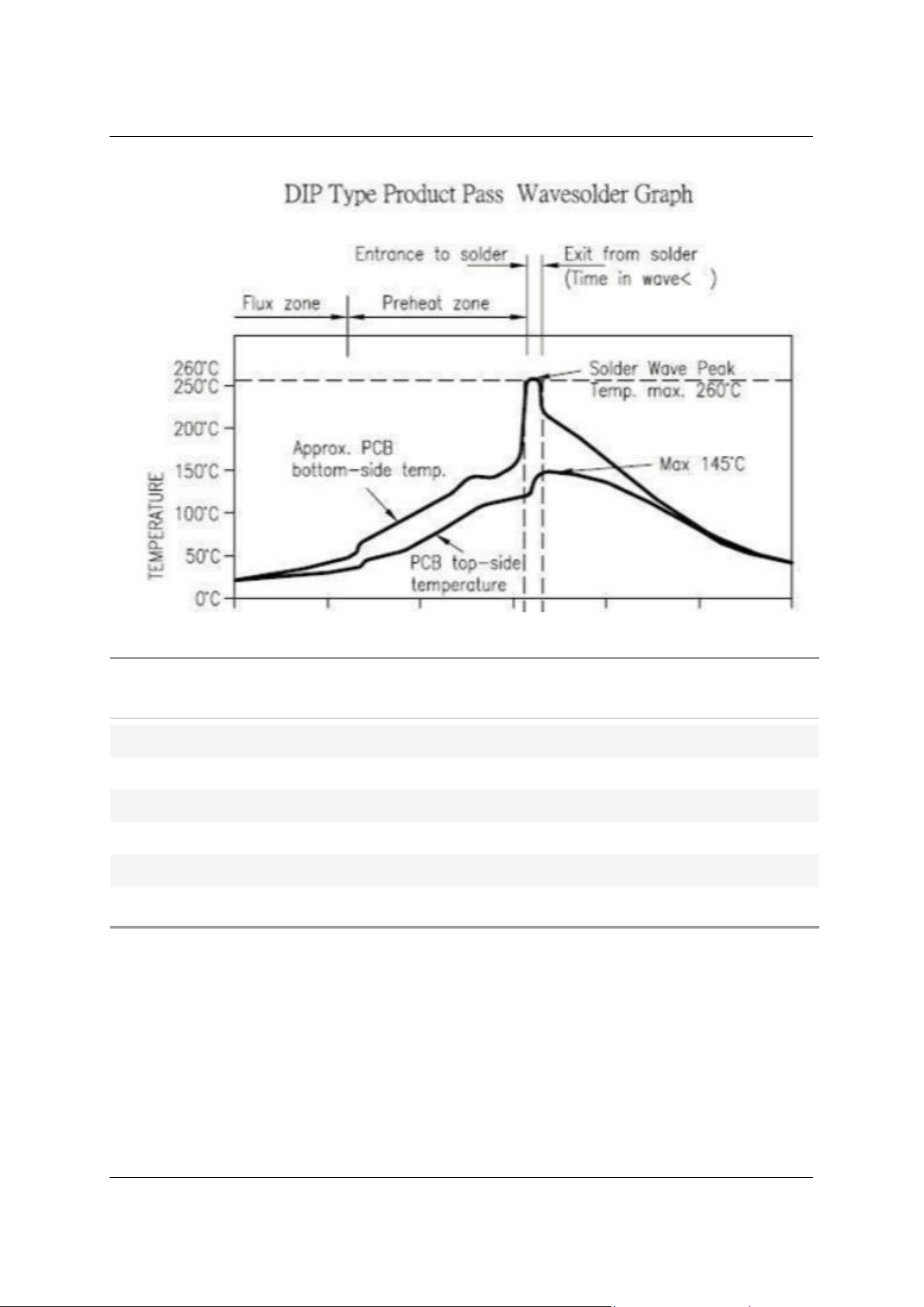
Method 2: Wave soldering process (wave soldering furnace temperature curve)
Please refer to the recommended furnace temperature for wave soldering. The peak temperature is 260
°C ±5°C , and the wave soldering temperature curve is shown in the figure below:
6 Packaging Information and Production Guidelines
20
/
20
Recommended temperature
curve for wave soldering
furnaces
Recommended temperature for manual welding repair
Preheating time
75-100S
Weld period
Less than 3S/point
Wave peak contact time
3-5S
NA
NA
Cylinder temperature
260± 5℃
NA
NA
Temperature Increase Slope
≤2℃/S
NA
NA
Cooling slope
≤6℃/S
NA
NA
360℃± 20℃
Welding temperature
80-130℃
Preheat temperature