
1 / 10
UBM2 User Guide
Table of Contents
1. Introduction ........................................................................................................................................ 2
1.1 Module Features .................................................................................................................... 2
1.2 Interface Definition ................................................................................................................. 3
2. Test Setup Details .......................................................................................................................... 4
3. Application Usage ........................................................................................................................... 5
3.1 Tx Application Usage ......................................................................................................... 5
4. FCC Statement ................................................................................................................................ 8
5, Integration instructions for host product manufacturers according to KDB 996369
D03 OEM Manual v01r01 ..................................................................................................................... 9
2 / 10
1. Introduction
The purpose of this document is to provide the usage of the applications for transmit and
receive tests to evaluate the RF performance of the UBM2 using a test driver in windows
environment. The evaluation board provides the necessary connectors so that you can
measure transmit, using Spectrum Analyzer and Signal Generator.
In general, transmit performance of a radio can be analyzed in three steps.
Maximum power: The user can observe the RF output power for a given maximum gain
supported by the RF.
The document contains three major sections.
Section 3.1 describes the usage of the ‘BT transmit’ utility, which provides the options for
setting various parameters to carry out transmit tests on the UBM2 device.
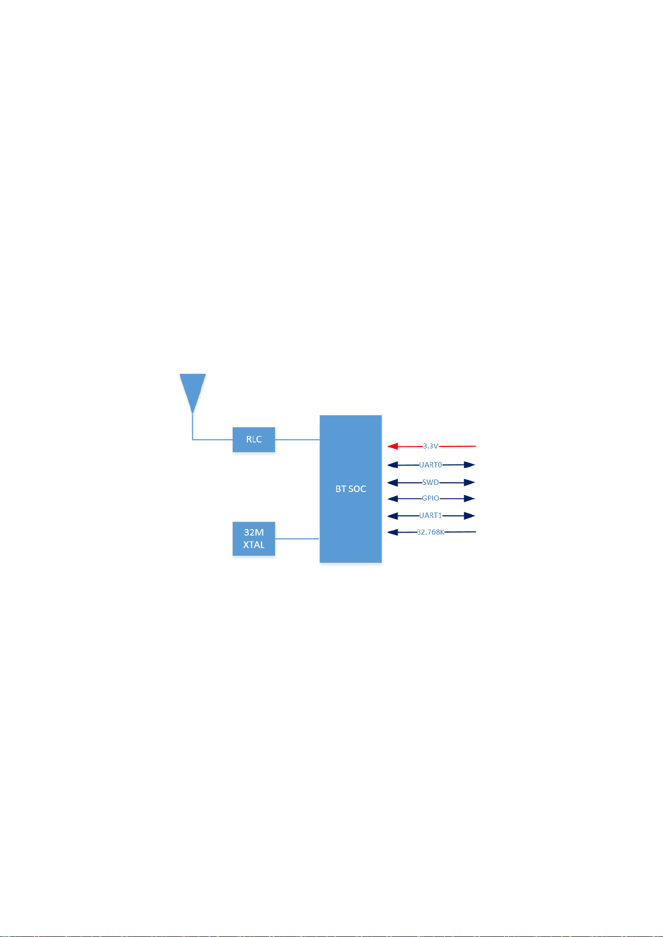
This UBM2 module is a single-mode, low-cost BLE5.1 Bluetooth module. It features
transparent transmission, active, passive, and master-slave integrated modes, and is
suitable for most Bluetooth application scenarios. It is also compatible with on-board
antennas and position antennas, and the actual application can be selected according to
product requirements.
Block diagram of the UBM2 system
1.1 Module Features
Processor
● ARM Cortex-M4 32-bit processor.
● The maximum main frequency can reach up to 64MHz.
Memory
● 512KB Flash: Support XIP to run code or save user data.
● 64KB Data SRAM: Code can be run or variables saved
● 8KB Code Cache: Used for Flash XIP code caching
RF Performance
3 / 10
The module integrates a high-performance 2.4GHz RF transceiver that meets the
requirements of Bluetooth RF. The features are as follows:
● Working frequency: 2.4G~2.4835GHz
● Modulation mode: GFSK
● Transmission rate: 1Mbps/2Mbps
● Transmission power: -20~9dBm Adjustable
● Receiving sensitivity: -95.5dBm@1Mbps/-93dBm@2Mbps
● Built-in Balun circuit, supporting single-ended RFIO output
Power Consumption
● Power supply: 3.3V
● Transmission mode: 6.4mA@0dBm Tx power
● Receiving mode: 7.4mA
● Sleep mode: 6.3uA@32K RTC runs and all SRAM contents remain
● OFF mode: 0.8 uA
Oscillator
● Support 32M XTAL
Peripheral interface
● 2-way UART interface
● 2-way SPI interface
● PWM
● SWD debugging
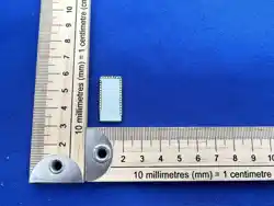
● Size: L26.0±0.2mm *W13 ±0.2mm*H1.9±0.5mm MAX
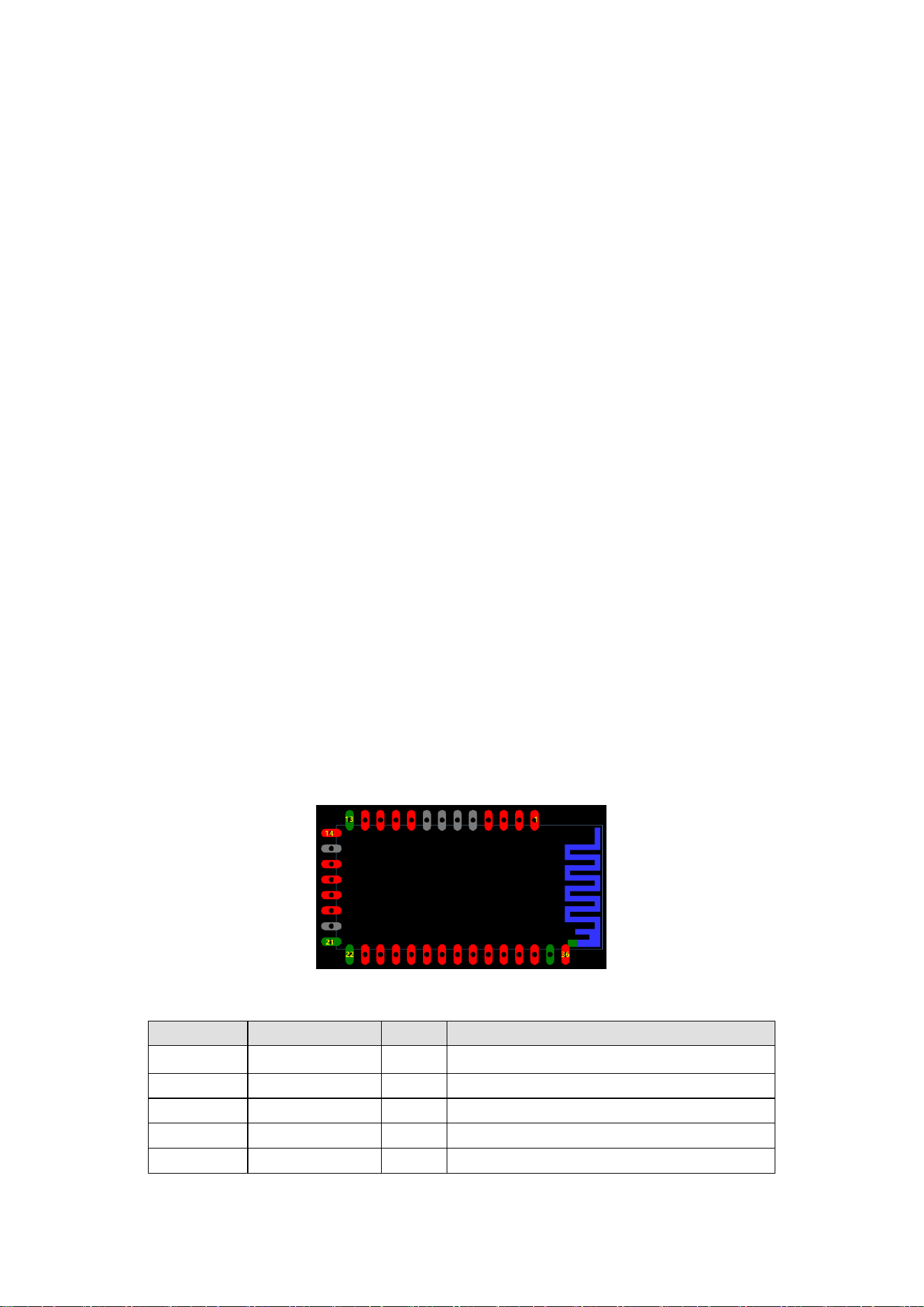
1.2 Interface Definition
Figure 2 Module pin diagram
Pin number
Pin name
Type
Pin function
1
P09/UART1_TX
I/O
UART_TXD
2
P10/UART1_RX
I/O
UART_RX
3
P20
I/O
General input and output
4
P21
I/O
General input and output
5
NC
/
Reserved

4 / 10
6
NC
/
Reserved
7
NC
/
Reserved
8
NC
/
Reserved
9
P11/Tran
I/O
General input and output
10
P12/Disc
I/O
General input and output
11
RST_N
I/O
Reset signal input, level valid
12
VDD33
I/O
3.3V power input
13
GND
P
Ground
14
P04/BOOT
P
Low level for Programming mode.
15
NC
/
Reserved
16
P00/SWCLK
I/O
SWD debug CLK input
17
P01/SWDIO
I/O
SWD debug data input
18
P05/UART0_TX
O
Output in programming mode.
19
P06/UART0_RX
I
Input pin in programming mode.
20
NC
/
Reserved
21
GND
P
Ground
22
GND
P
Ground
23
XTAL32K_OUT
O
32.768KHz Crystal oscillator output
24
XTAL32K_IN
I
32.768KHz Crystal oscillator input
25
P27
I/O
General input and output
26
P26
I/O
General input and output
27
P03
I/O
General input and output
28
P25
I/O
General input and output
29
P24
I/O
General input and output
30
P07
I/O
General input and output
31
P08
I/O
General input and output
32
P23
I/O
General input and output
33
P02
I/O
General input and output
34
P22
I/O
General input and output
35
GND
P
Ground
36
ANT
I/O
RF Port
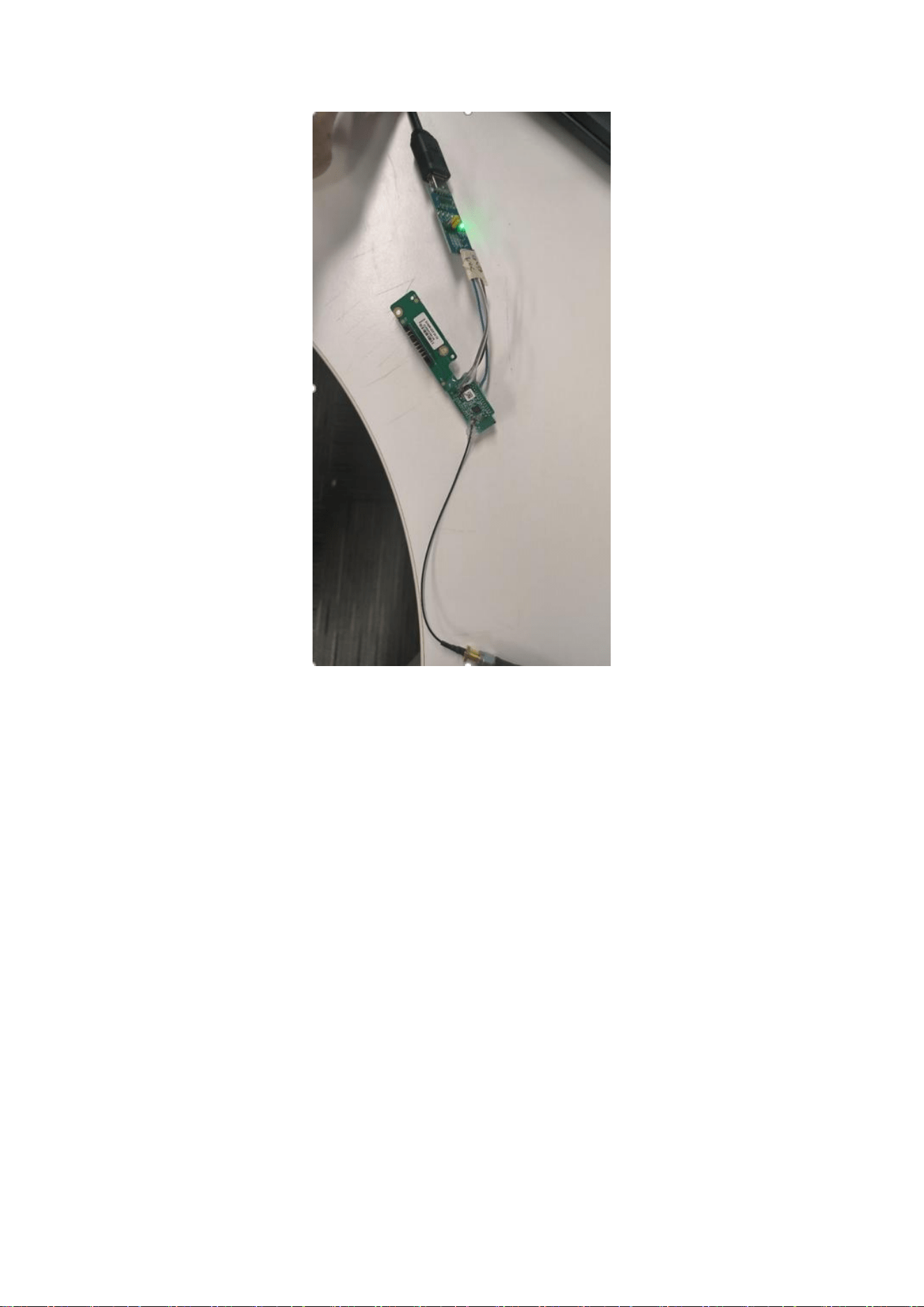
2. Test Setup Details
The diagram shown below, illustrates the test setup for transmit performance of UBM2
module.
As shown in the test setup, the UBM2 evaluation board (EVB) is connect to pc via UART.
The board is connected to a signal analyzer through a microwave coaxial cable to test
the Tx or Rx performance.
Figure 1: Based RF Evaluation Setup Interface
Following diagram illustrates various software components involved in performing Tx and
Rx tests using spectrum analyzer and signal generator respectively.
5 / 10
The ‘transmit ’ utility is a command line application to perform Tx tests. Before running
the Tx tests, the user is expected to connect UBM2 module to a signal analyzer using the
RF cable.
The ‘receive’ utility is also a separate command line application that can be used for
displaying statistics on the received packets while carrying out the receive sensitivity
tests.
3. Application Usage
3.1 Tx Application Usage
The application can be started in the following steps:
plug UART EVB into the device and laptop, check the laptop’s UART number and set up
the serial port tool Portland, send the command via UART tools.
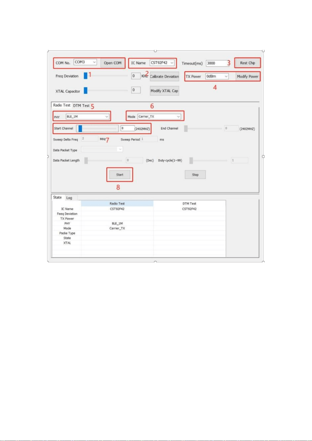
1、 Singel tone test
6 / 10
Power on module
1. Select the COM port
2. Select chip ID
3. Rest Chip
4. Select TX Power (default is 0 dBm)
5. Select PHY rate
6. Select test mode
7. Set the test channel
8. Start
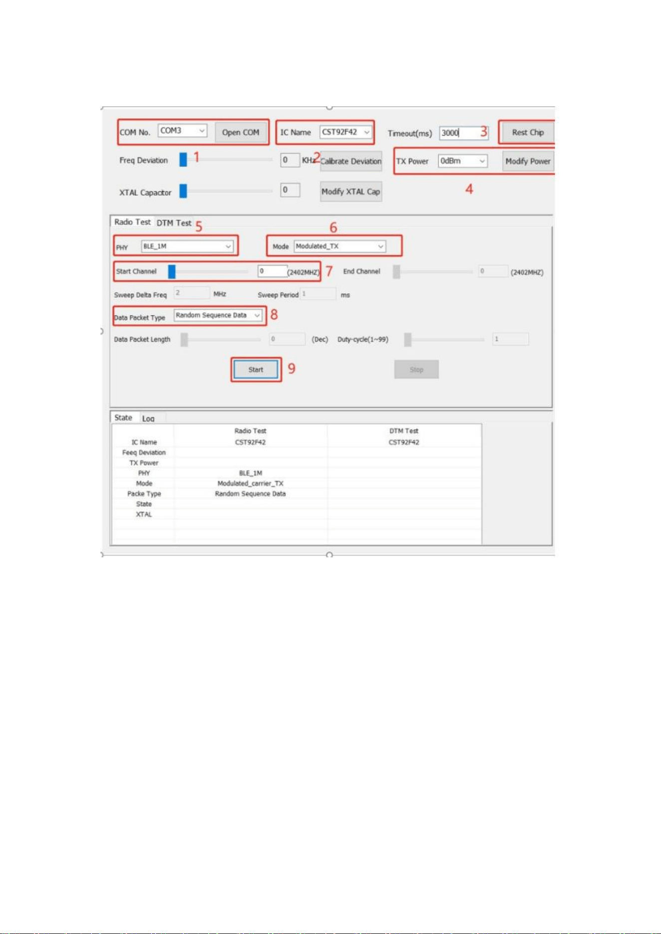
2、 TX power test
7 / 10
Power on module
1. Select the COM port
2. Select chip ID
3. Rest Chip
4. Select TX Power (default is 0 dBm)
5. Select PHY rate
6. Select test mode
7. Set the test channel
8. Select the data packet Type
9. Start

8 / 10
4. FCC Statement
This Module complies with part 15 of the FCC rules. Operation is subject to the following two conditions: (1) this mod
ule may not cause harmful interference, and (2) this module must accept any interference received, including interf
erence that may cause undesired operation.
Changes or modifications not expressly approved by the party responsible for compliance could void the user’s
authority to operate the equipment.
NOTE: This equipment has been tested and found to comply with the limits for a Class B digital device, pursuant
to part 15 of the FCC Rules. These limits are designed to provide reasonable protection against harmful interference i
n a residential installation. This equipment generates uses and can radiate radio frequency energy and, if not
installed and used in accordance with the instructions, may cause harmful interference to radio communications. How
ever, there is no guarantee that interference will not occur in a particular installation. If this equipment does cause har
mful interference to radio or television reception, which can be determined by turning the equipment off and on, the u
ser is encouraged to try to correct the interference by one or more of the following measures:
‐ Reorient or relocate the receiving antenna.
‐ Increase the separation between the equipment and receiver.
‐ Connect the equipment into an outlet on a circuit different from that to which the receiver is connected.
‐Consult the dealer or an experienced radio/TV technician for help important announcement
Radiation Exposure Statement
The module has been evaluated to meet general RF exposure requirement. The device can be used in portable
exposure condition without restriction.

9 / 10
5, Integration instructions for host product manufacturers
according to KDB 996369 D03 OEM Manual v01r01
5.1 List of applicable FCC rules
CFR 47 FCC PART 15 SUBPART C(§15.247) is applicable to this modular transmitter.
5.2 Specific operational use conditions
There are no specific operational use conditions for the module.
5.3 Limited module procedures
The module has no own RF shielding and has been granted a limited modular approval (LMA). As grantee of the
EDAN INSTRUMENTS, INC is responsible for approving the host environment that the module is used with. Thus,
the host manufacturer must observe the following procedure to ensure host compliance:
a). EDAN INSTRUMENTS, INC must review and release the host environment prior to giving the host manufacturer
approval.
b). The module is to be installed by trained and qualified personnel only.
c). The host integrator installing the module must ensure that the final composite product complies with the FCC
requirements by a technical assessment or evaluation to the FCC rules.
d). A Class II Permissive Change is required for each specific host installation.
5.4 Trace antenna designs
N/A
5.5 RF exposure considerations
The modular is approved for portable use and is permit to installed in host device with following RF exposure conditions,
these RF exposure conditions must be stated in the end-product manual(s) of the host device manufacturer clearly:
⚫ Portable - 0cm from a person’s body
⚫ Mobile - Greater than 20cm from a person’s body
However,When the module is used in any other way it is granted, such as portable to mobile or with other transmitters
simultaneously, requires additional evaluation/testing and Class 2 permissive change.
5.6 antenna
This module has been approved by Federal Communications Commission to operate with the antenna types listed
below, with the maximum permissible gain indicated. The antenna is permanently fixed. It cannot be replaced.
Model Name
Frequency Band
Type
Peak Gain (dBi)
2.4 ANT
2400-2500MHz
PCB antenna
1.1 dBi
5.7 Label and compliance information
The final-end product must be labeled in a visible area with the following" Contains FCC ID: SMQIM3 "
5.8 Information on test modes and additional testing requirements

10 / 10
The designated C2PC test plan is as follows:
a) Testing should be done by an FCC recognized testing Laboratory and tests are based on C63.10-2020;
b) Host manufacturer should contact the module manufacturer for access to test mode software for configuring transmit
channel and modulation.
c) Measure the Maximum Peak Output Power according to §15.247(b)(3) on Channel 00/19/39 and modulation
(1&2Mbps).
d) Measure Radiated spurious emission from 9kHz to 25GHz according to § 15.209 on Channel 00/19/39 and
modulation (1Mbps).
e) Measure Radiated Band-edge according to §15.205&§15.209 on Channel 00/39 and modulation (1Mbps).
f) Measure AC power conducted emissions according to §15.207 in the case the host device is designed to be
connected to the public utility (AC) power line.
Note 1: If the C2PC investigation indicates that the module's conducted power has increased from the original filing
test report, the manufacturer, lab, and TCB must investigate to determine if the initial module tested in a standalone
module was improperly granted. The module may require a new FCC ID. An inquiry can be submitted to review a
specific case, but the C2PC can only be given once the issue is resolved.
Note 2: An increase in measured field strength over the module’s tested field strength is the result of host installation,
such as signal reflections, and this increased field strength value remains compliant with the rules. In that case, a
statement is required in the C2PC test report, such as “An increase in measured field strength over the original
tested field strength has been investigated and determined to be due to host installation.”
Note 3: Any radiated emission that does not comply with regulations must be corrected, and the C2PC can only be
granted once the issue is resolved.
5.9 Additional testing, Part 15 Subpart B disclaimer
The modular transmitter is only FCC authorized for the specific rule parts (FCC part 15.247) listed on the grant, If the
final host product contains unintentional-radiator digital circuity, the final host product still requires Part 15 Subpart B
compliance testing with the modular transmitter installed.
5.10 Note EMI Considerations
The host product shall be evaluated for ensuring the continuous compliance for the FCC rules that apply to the host
product. The testing should check for emissions that may occur due to the intermixing of emissions with the other
transmitters, digital circuitry, or due to physical properties of the host product(enclosure). Additional guidance for
testing host products is provided in KDB Publication 996369 D02 and D04 (For standalone mode, reference the
guidance in D04 Module Integration Guide and for simultaneous mode, see D02 Module Q&A Question 12, which
permits the host manufacturer to confirm compliance).
5.11 How to make changes
Only module Grantee are permitted to make permissive changes, Please contact us for further process at:
Contact Name: EDAN INSTRUMENTS, INC.
Phone: 0755-26682547
Website: www.edan.com.cn
E-mail: xiahuanhu[email protected].cn14
Address: #15 Jinhui Road, Jinsha Community, Kengzi Sub-District, Pingshan District,518122 Shenzhen P.R.China