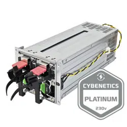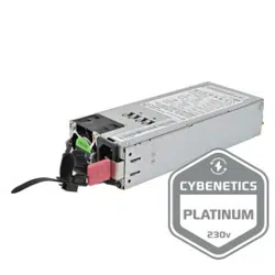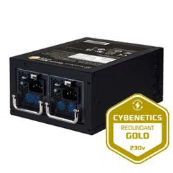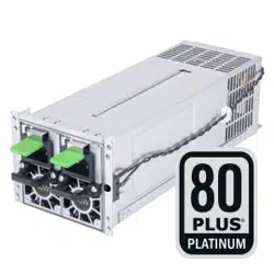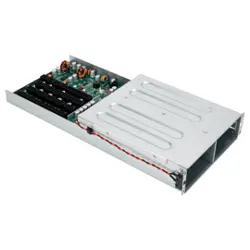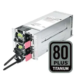

Gemini 2000C Titanium / Gemini 2400C Titanium
Gemini Series
80PLUS Titanium 2000W+2000W / 2400W+2400W 2U CRPS
Redundant Power Supply
●2000W + 2000W 24-hour continuous performance, reliably operating at 50°C
with fully sustained power output.
●2400W + 2400W 24-hour continuous performance, reliably operating at 50°C
with fully sustained power output.
●2 x native 12V-2x6 connectors with cables included, supporting RTX 40/50 series GPUs
●2U CRPS form factor: 82mm (W) x 101.5mm (H) x 210mm (D)
●80PLUS Titanium certification
●Active PFC (full range)
●All Japanese electrolytic capacitors, polymer capacitors
●Hot-swappable design
●Convenient pull-out handle bars
●Support PMBus 1.2

SPECIFICATION
SilverStone Gemini Series
Gemini 2000C Titanium
Gemini 2400C Titanium
SST-GM2000C-TF
SST-GM2400C-TF
1+1 2U CRPS Redundant Power Supply
80PLUS Titanium efficiency certified.
2000W
2400W
01
1.GENERAL SCOPE
This specification describes the performance characteristic of a DC-DC
Switching power distribution Board (PDB) with a +12V main DC input and
+12Vsb auxiliary input.
The PDB will switch into +3.3V, +5V, -12V, +5Vsb auxiliary output and
distribute +12V main output to the system.
The PDB shall be able to operate with a single power supply module or in
1+1 parallel. Power module shall support hot-plug and active load share for
+12V main output. This PDB can support all the Common Slot module which
is meet CRPS design guide including AC/LVDC/HVDC input and mixed
operation of different input type of power supply module are also allowed.
The physical size of the power supply enclosure is intended for accommo-
date the power range of up to 2000W/2400W. The physical size is 210mm x
76.5mm x 83mm (length x width x height)
1.1. Mechanical Overview
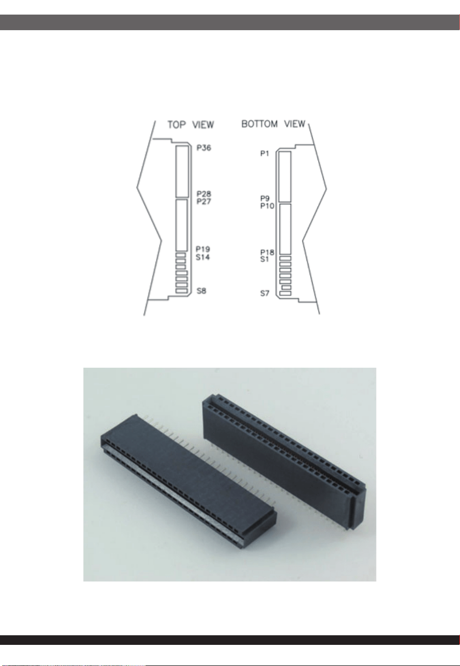
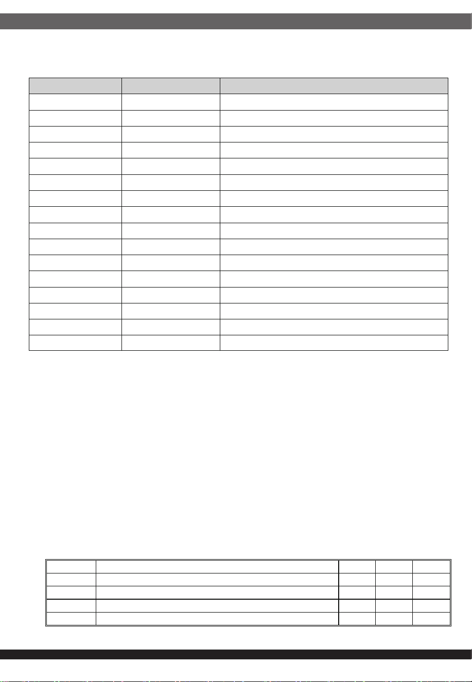
1.2.Power supply card edge connector (Power module gold finger pin definition)
The power supply card edge pinout is defines in the below table. This card edge
is compatible with OUPIIN 9393-F2P50N11ACB30DA or equiv. at PDB side.
02
Figure 2-1 – Top view Output connector
Figure 2-2 – Bottom view Output connector
Figure 3 – PDB Card edge connector
03
Table 1 – Power module gold finger pin assignment
1.3.Environmental Requirements
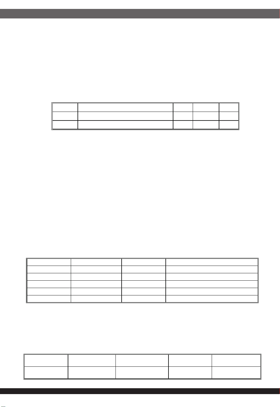
1.3.1.Temperature and Humidity Requirements
Pins Function Description
P1-P9, P28-P36 GND Main Return and Standby Return
P10-P18, P19-P27 +12.2V +12.2V Main output
S1 A0 Address pin 0
S2 A1 Address pin 1
S3 +12VSB 12V standby output
S4 C_R Cold Redundancy
S5 +12VLS +12V Load share bus
S6 PRESENT Power supply present signal
S7 INPUT_OK Input voltage ok signal
S8 PW_OK Output voltage OK signal
S9
+VSENCE
+12V Remote Sense
S10
-VSENCE
12V standby Return sense.
S11 SMB_Alert
#
PS Alert signal for failure notification
S12 PSON +12V output on/off control signal
S13 SCL PMBus Clock
S14 SDA PMBus Data
The power supply shall operate within all specified limits over specified condi-
tions in 2.3.
The defined operation condition includes temperature, humidity, altitude, shock
and vibration.
The power supply shall operate within all specified limits over Top temperature
range and specified humidity Range. All airflow shall pass through the power
supply and not over the exterior surfaces of the power supply.
The power supply shall withstand thermal storage specified in Tnon-OP without
any damage.
Table 2 – Temperature Requirements
Item Description MIN MAX Unit
T
OP
Operating temperature range. -5 50 °C
T
non-OP
Non-Operating temperature range. -40 70 °C
HOP Operating humidity range, non-condensing 5 85 %
H
non-OP
Non-Operating humidity range, non-condensing 95 %
04
1.3.2.Altitude Requirements
The power supply shall operate within all specified limits over Aop Altitude
range. The change pressure condition shall not harm the power supply and the
operation within specified regulations shall be assured.
The power supply shall withstand Altitude storage specified in Anon-OP without
any damage.
Table 3 – Altitude Requirements
The power supply shall operate within all specified limits over Aop Altitude
range. The change pressure condition shall not harm the power supply and the
operation within specified regulations shall be assured.
The power supply shall withstand Altitude storage specified in Anon-OP without
any damage.
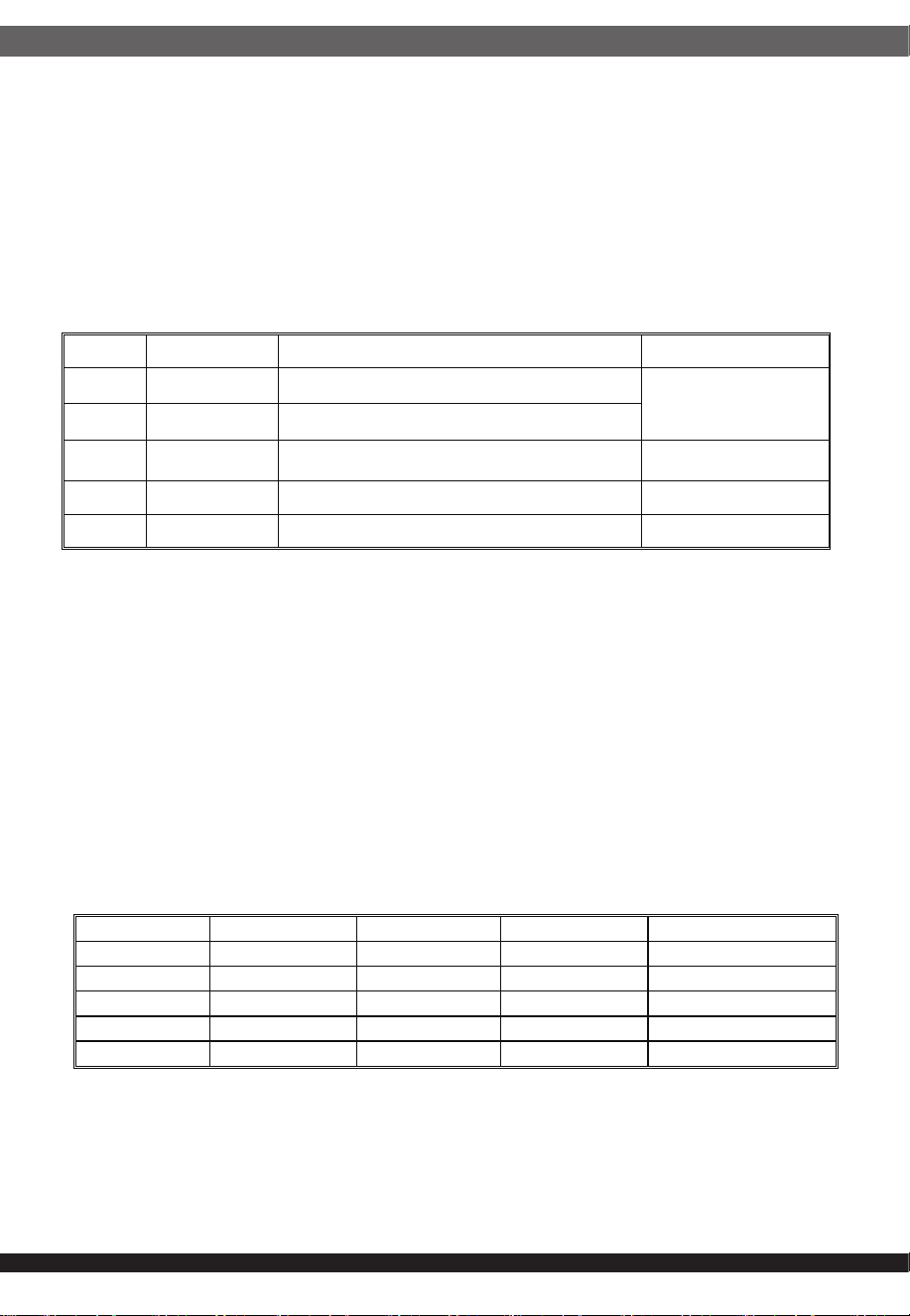
2.1.Input Specification(Refer to Module input voltage type)
2.1.1.Input voltage and frequency specification
The power supply shall supply the full output power in the voltage range of
90VAC to 264VAC or 190HVDC to 310HVDC.
2.1.1.1. LVDC Input voltage
The power supply shall supply the full output power in the voltage range of
-40VDC to -72VDC.
Table 4 – Rated output power for each input voltage range
Table 5 – Rated output power for each input voltage range
Item Description MIN MAX Unit
A
OP
Operating Altitude range. 0 5000 m
A
non-OP
Non-Operating Altitude range. 0 15000 m
2.ELECTRICAL PERFORMANCE
Parameter Minimum input Rated Input Maximum input
115 VAC 90V
rms
100-127V
rms
140V
rms
230 VAC 180V
rms
200-240V
rms
264V
rms
Frequency 47Hz 50/60Hz 63Hz
HVDC Input
240HVDC 190HVDC 190-310HVDC 310HVDC
Parameter Min. input Rated Input Max. input V
PEAK
-48VDC -40VDC
-40 to -72VDC
-72V
DC
-75VDC
<1sec
05
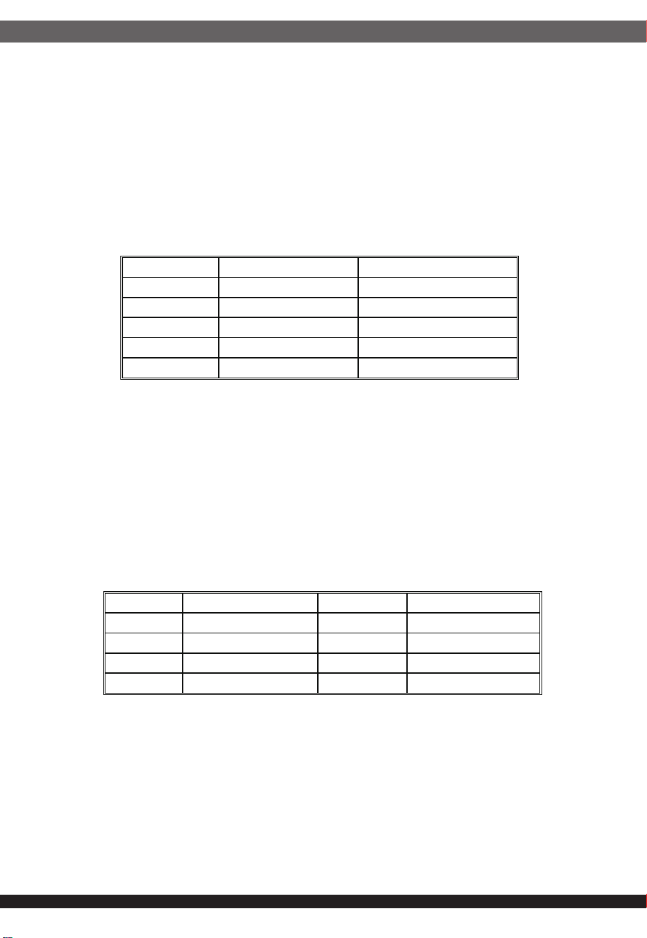
Table 7 – Output Power and Current Ratings
Note: The output voltage regulator is set from 11.59V to 12.81V when the power
module is set from 1600W to 2000W.
Table 8 – Output Voltage regulation
2.2.DC output voltages
2.2.1.Output rating
The following table defines the power and current rating of the 2000W and
2400W power supply. The combined output power of all outputs shall not
exceed the rated output power. The power supply must meet both static and
dynamic voltage regulation requirements.
2.2.2. Auxiliary Output (Standby)
The 5Vsb output shall be present when input greater than Vrecover is applied.
2.2.3. No load operation
The power supply shall meet all requirements except for the transient loading
requirements when operated at no load on all outputs.
2.2.4. Voltage Regulation
The power supply shall meet the voltage regulation under all operating condi-
tions (input line, transient loading, output loading). These limits include the
peak-peak ripple/noise. The regulation of Table 8 shall be measured at the
output connector of the power supply, subject to the dynamic loading conditions
in Table 10.
Output Minimum Load Maximum Load Condition
+3.3V 0A 25.0A
+3.3V & +5V
combined power
≤ 180W
+5V 0A 36.0A
+12V 0.5A 160A(2000W*)/196A(2400W*)
*Low line input:
Output power :1000W
-12V 0A 0.5A
+5VSB 0A 3A
Output Minimum Nominal Maximum Unit
+12V 11.4 12.0 12.6 V
+5V 4.75 5.0 5.25 V
+3.3V 3.135 3.3 3.465 V
-12V -11.40 -12.0 -12.6 V
+5Vsb 4.75 5.0 5.25 V
06
2.2.5.Ripple and Noise Regulation
Ripple and Noise are defined in table 9. Ripple and Noise shall be measured
over a Bandwidth of 0Hz to 20MHz at the power supply output connector. A 0.1
μF ceramic capacitor and 47μF of tantalum capacitor shall be placed at each
point of measurement. The measurement points shall be as close as possible to
the point of load.
The ripple and noise specification shall be met over all load ranges and input
line voltages with 1+1 power supplies in parallel operation.
2.2.6.Dynamic loading
The power supply shall operate within specified limits and meet regulation
requirements for step loading and capacitive loading specified below.
The load transient repetition rate shall test between 50Hz to 5 KHz at duty
cycles ranging. The load transient repetition rate is only a test specification. The
Δ step load may occur anywhere within the MIN load and the MAX load.
2.2.7.Capacitive load
The power supply shall operate within specifications over the capacitive loading
ranges defined below in Table 11.
Table 9– Ripple and Noise Regulation
Table 10 – Transient Load Requirements
Output Maximum Unit
+12V 120 mV
+5V 50 mV
+3.3V 50 mV
-12V 120 mV
+5Vsb 50 mV
Output Δ Step size Slew Rate Capacitive Load
+3.3V 30% OF MAX. 1A/μs 2200μF
+5V 30% OF MAX. 1A/μs 2200μF
+12V 60% OF MAX. 1A/μs 4700μF
+5Vsb 25% OF MAX. 1A/μs 100μF

07
Table 11 – Capacitive Loading Conditions
Output Min Max
+3.3V 100μF 12,000μF
+5V 100μF 12,000μF
+12V 100μF 12,000μF
-12V 1μF 350μF
+5Vsb 1μF 350μF
2.2.8.Closed loop stability
The power supply shall be unconditionally stable under all line/load/transient
load conditions including capacitive load ranges. A minimum of: 45 degrees
phase margin and -10dB gain margin is required.
Closed-loop stability must be ensured at the maximum and minimum loads as
applicable.
2.2.9.Residual Voltage Immunity in Standby mode
The power supply should be immune to any residual voltage placed on its
outputs (typically a leakage voltage through the system from standby output) up
to 100mV. There shall be no additional heat neither generated nor stressing of
any internal components with this voltage applied to any individual or all outputs
simultaneously. It also should not trip the protection circuits during turn on/off.
The residual voltage at the power supply outputs for no load condition shall not
exceed 100mV when AC voltage is applied.
2.2.10.Soft starting
The power supply shall contain control circuit, which provides monotonic soft
start for its outputs without overstress of the input line or any power supply
components at any specified input line or load condition.
2.2.11.Hot Swap Requirements
Hot swapping a power supply is the process of inserting and extracting a power
supply from an operating power system. During this process, the output voltag-
es shall remain within the limits with the capacitive load specified.
The hot swap test that must be conducted when the system is operating at
under static, dynamic, and zero loading conditions. The power supply shall use
a latching mechanism to prevent insertion and extraction of the power supply
when the AC/HVDC and LVDC power cord is inserted into the power supply.
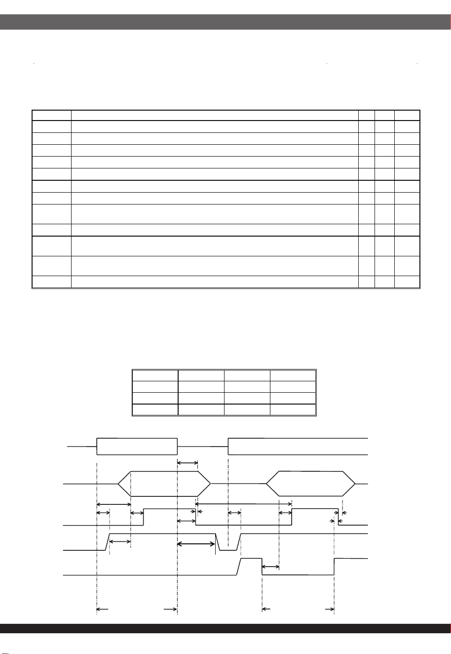
2.3.Timing Requirements
These are the timing requirements for the power supply operation. The output
voltages must rise from 10% to within regulation limits (Tvout_rise) within 10 to
70ms. For 5Vsb, it is allowed to rise from 1 to 25ms. All outputs must rise
monotonically. Table below shows the timing requirements for the power supply
being turned on and off via the AC input, with PSON held low and the PSON
signal, with the AC input applied.
08
2.3.1.Output Voltage Timing
The timing of signals and outputs are specified in below Table 12 and illustrated
in Figure 4.
*Tvout_rise: The 5Vsb and -12V output rise time shall be 1ms to 20ms.
*T5Vsb_holdup: The minimum time is 40msec when the PDB uses PSU module
of the LVDC input.
* Tvout_holdup and Tpwok_holdup are limited as the below table.
Figure 4 – Turn On/Off Timing (Power Supply Signals)
Table 12 - Turn on/off timing
Turn on Description Min Max Units
T
vout rise
Output voltage rise time for all main output. 1* 80* msec
T
sb_on_delay
Delay from input being applied to 5Vsb being within regulation. 1500 msec
T
ac_on_delay
Delay from input being applied to all output voltage being within regulation. 2500 msec
T
vout_holdup
Time all main output 12VF voltages stay within regulation after loss of input. 4 msec
T
pwok_holdup
Delay from loss of input to de-assertion of PWOK. 3 msec
T
pson_on_delay
Delay from PSON
#
active to output voltages within regulation limits. 5 400 msec
T
pson_pwok
Delay from PSON
#
deactivate to PWOK being de-asserted. 50 msec
T
pwok_on
Delay from output voltage (12V) within regulation limits to PWOK asserted at turn
on.
100 500 msec
T
pwok_off
Delay from PWOK de-asserted to output voltages dropping out of regulation limits. 1 msec
T
pwok_low
Duration of PWOK being in the de-asserted state during an off/on cycle using input
or the PSON signal.
100 msec
T
sb_vout
Delay from 5Vsb being in regulation to main output being in regulation at input
turn on.
50 1000 msec
T
5Vsb_holdup
Time the 5Vsb output voltage stays within regulation after loss of input. 70* msec
PSU T
vout_holdup
T
pwok_holdup
unit
2000W 4 3 msec
2400W 4 3 msec
LVDC - - msec
Input
Vout
PWOK
5Vsb
PSON
T
sb_on_delay
T
AC_on_ delay
T
p
wok_on
T
vout_holdup
T
p
wok_holdup
T
p
son_on_delay
T
sb_on_delay
T
p
wok_on
T
p
wok_off
T
p
wok_off
T
p
son_pwok
T
p
wok_low
T
sb_vout
AC turn on/off cycle
PSON turn on/off cycle
T
5Vsb
_
holdup

09
Table 13 – PS ON# signal characteristics
Signal Type
3.3VDC, TTL compatible; Has a 2k ohm pull up resister
internal to the power supply.
PSON
#
= Low ON
PSON
#
= High or Open OFF
PSON
#
= Low, PSKILL = Open OFF
MIN MAX
Logic level low (power supply ON) 0V 0.8V
Logic level high (power supply OFF) 2.0V 3.46V
Source current, V
pson
= low 0.28mA
Power up delay: T
pson_on_delay
5ms 400ms
PWOK delay: T
pson_pwok
50ms
2.3.2.Overshoot
Any output overshoot at turn on shall be less than 5% of the nominal output
value.
2.3.3.Undershoot
Any output shall not undershoot at turn on or off cycle under any circumstanc-
es.
2.3.4.Temperature coefficient
After operating for 30 minutes or longer at 25° C ambient, the output voltages
shall not change by more than 0.05 % per degree C for any given line and
load conditions.
2.4.Control and Indicator functions
The following section defines the input and output signals from the power
supply.
Signals that can be defined as low true use the following convention:
Signal# = low true.
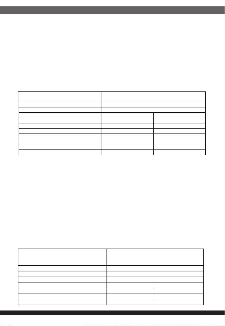
2.4.1.PSON# Input Signal (Power supply enable)
The PSON# signal is required to remotely turn on/off the main output of the
power supply.
PSON# is an active low signal that turns on the main output power rail. When
this signal is not pulled low by the system or left open, the outputs (except the
Standby output) turn off.
PSON# is pulled to a standby voltage by a pull-up resistor internal to the power
supply.
See Table 13.
+
-
10
Table 14 – PWOK signal characteristics
Table 15 – Smaller# signal characteristics
2.4.2.Power OK (PG or PWOK) Output Signal
PWOK is a power good signal and shall be pulled HIGH by the power supply to
indicate that all outputs are within regulation limits. When any output voltage
falls below regulation limits, an internal failure or when input power has been
removed for a time sufficiently long, so that power supply operation is no longer
guaranteed, PWOK will be de-asserted to a LOW state. The start of the PWOK
delay time shall inhibited as long as any power supply output is in current limit.
See Table 14.
2.4.3.SMBAlert# (PSAlert) Output Signal Pin
This signal indicates that the power supply is experiencing a problem that the
user should investigate. This shall be asserted due to Critical events or Warn-
ing events. The signal shall activate in the case of critical component tempera-
ture reached a warning threshold, general failure, over-current, over-voltage,
under-voltage, failed fan. This signal may also indicate the power supply is
reaching its end of life or is operating in an environment exceeding the speci-
fied limits.
This signal is to be asserted in parallel with LED turning solid red or blinking
Amber/Green. See Table 15.
Signal Type
3.3VDC TTL Compatible; Has a 2.4k ohm pull up
resister internal to the power supply
PWOK=High Power Good
PWOK=Low Power Not Good
MIN MAX
Logic level low voltage, I
sink
=4mA 0V 0.4V
Logic level high voltage, I
source
= 200μA 2.4V 3.46V
Sink current, PWOK=low 4mA
Source current, PWOK=high 0.2mA
PWOK delay: T
pwok_on
100ms 500ms
PWOK rise and fall time 100μsec
Power down delay: T
pwok_off
1ms 200ms
Signal Type
3.3VDC ,TTL Compatible; Has a 2.4k ohm Pull up
resister internal to the power
Alert
#
=High
Power OK
Alert
#
=Low Power Alert to system
MIN MAX
Logic level low voltage, I
sink
=4mA 0V 0.4V
Logic level high voltage, I
sink
= 50μA 2.4V 3.46V
Sink current, Alert
#
=low 4mA
Sink current, Alert
#
=high 0.2mA
Rise and fall time 100μsec

11
2.4.4.Remote Sense
The power supply has remote sense return (Return Sense) to regulate out ground
drops for all output voltages. The power supply uses remote sense to regulate out
drops in the system for the main outputs of +3.3V, +5V, +12V. The +3.3V,+5V and
+12V output only uses remote sense with reference to the Return Sense signal.
The remote sense input impedance to the power supply must be greater than 10Ω
on the main outputs and 10Ω on Return Sense. These are the values of the
resistors connecting the remote senses to the output voltage internal to the power
supply. Remote sense is able to regulate out a minimum of 200mV of drop on the
+3.3V, +5V and +12V outputs. The remote sense return is able to regulate out
drops of 200mV as well. The current in any remote sense line shall be less than
5mA to prevent voltage-sensing errors. The power supply operates within specifi-
cation over the full range of voltage drops from the power supply’s output connec-
tor to the remote sense points.
2.4.5.SDA and SCL
One pin is the serial clock (SCL), and the other pin is used for serial data (SDA).
The SCL and SDA signals are pulled up by system, both pins are bi-directional,
open drain signals, and are used to form a serial bus.
3.Protection circuits
Protection circuits inside the power supply shall cause only the main output to
shutdown (latch off). If the power supply latches off due to a protection circuit
assert, an Input Power cycle OFF for 15sec or a PSON# cycle HIGH for 1sec
shall be able to reset the power supply.
Specific protection circuits shall not latch, but auto recover when the latching
reason had been cleared. This protection circuits will be written in cursive writing
and will have an Auto Recover (OutputAr) in the chapter name.
The auxiliary output shall not affect by any protection circuit, unless the auxiliary
output itself is affected.
3.1.Over Voltage Protection (OVPmain & OVPauxilary AR)
All Over Voltage Condition shall be measured internal to the power supply on all
outputs (Main and Auxiliary OutputAR). The power supply shall shutdown and
latch off after an Over Voltage condition occurs on main outputs, the auxiliary
output shall be auto recover (VsBAR) after the OVP had been removed.
The voltages never shall exceed the maximum levels specified in below table
when measured during any fail.
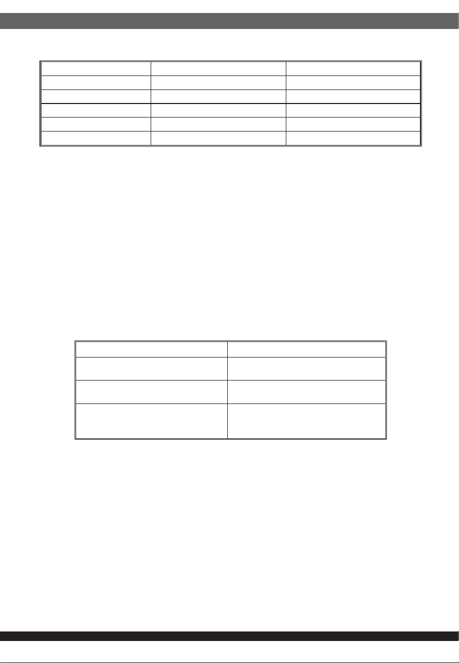
The power supply shall alert the system of the OCP/SCP condition via SMBAlert#
and fail LED indicator.
The latch on the main output can be cleared by asserting the PSON# signal or by
an Input Power interruption.
12
Table 16 - Over Voltage Protection requirements
Table 17 – Over Current/Short Circuit Protection
Output Voltage MIN (V) MAX (V)
+3.3 V 3.9 4.5
+5 V 5.7 6.5
+12 V 13.3 14.5
-12 V -13.3 -14.5
+5Vsb 5.7 6.5
3.2.Over Current and Short Circuit Protection
(OCP/SCPmain & OCP/SCPauxilary AR)
The Over Current Condition shall be measured internal to the power supply on all
outputs (Main and Auxiliary OutputAR), and preventing outputs to exceed current
limits specified in below table. The power supply shall be auto recover (VsBAR)
after the OCP/SCP had been removed.
The latch on the main output can be cleared by asserting PSON# signal or by an
Input Power interruption.
The power supply shall alert the system of the OCP/SCP condition via SMBAlert#
and fail LED indicator.
The power supply shall not be damaged from repeated power cycling in this
condition.
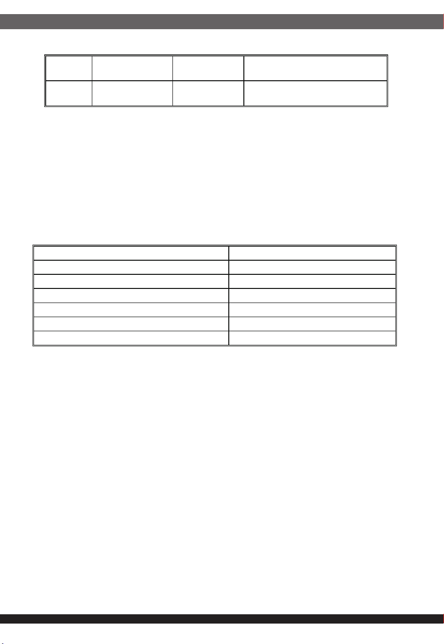
3.3.Over Temperature Protection (OTPAR)
The PDB shall have a thermal sensor to measure the environmental (Tenv). The
thermal sensor shall be part of a protection circuit to protect against over tempera-
ture conditions caused by loss of fan cooling or excessive ambient temperature.
In a critical Over temperature condition, specified in below table, the power
system shall be shutdown with the exception of the auxiliary output (VSBAR ).
The Thermal CLST shall be part of the OTPAR.
The PDB shall alert the system of the OTPAR condition via SMBAlert# and
Buzzer. The PDB will auto recover the power system from this condition, when
the temperature is dropping within specification again. If the OTPAR is caused
due to a defective fan in the power module, than the defective module shall latch
off and not auto recover.
Voltage
Over Current Limit (Iout limit)
+3.3 V 110% minimum; 150%
maximum(27.5~37.5A)
+5 V 110% minimum; 150% maximum
(39.6~54A)
+12 V 110% minimum; 139% maximum
2000W(176A~222.4A)
2400W(215.6A~272.44A)
13
Table 18 – Over Temperature Protection
Table 19 – Buzzer Status Information
3.4.Fault indication
When one of the power supply module in the system fails to provide output, the
system shall provide below alarm signal to the system.
3.4.1.Audible alarm
3.4.1.1 Buzzer Sound and identification
The PDB shall have a Buzzer for indication of the power system status for
audible alarm. The buzzer is derived by an internal circuitry and should sound in a
1+1 configuration even without input power.
The Buzzer function can turn off by hardware.
3.5.Hardware Layer
The serial bus communication devices for Power Supply Management Controller
(PSMC) and Field Replacement Unit (FRU) in the power supply shall be compati-
ble with both SMBus 2.0 “high power” and I2C Vdd based power and drive
specification.
This bus shall operate at 3.3V but be tolerant to 5V pull-ups. The power supply
should not have any internal pull-ups on the SMBus; pull-ups shall be located on
system side.
Two pins are allocated on the power supply. One pin is the serial clock (SCL).
The second pin is used for serial data (SDA). Both pins are bi-directional and are
used to form a serial bus. The device(s) in the power supply shall be located at an
address(s) determined by addressing pins A0 and A1 on the power supply
module. The circuits inside the power supply shall derive their 3.3V power from
the 5Vsb bus through a buffer. Device(s) shall be powered from the system side
of the 5Vsb oring device. No pull-up resistors shall be on SCL or SDA inside the
power supply. The pull-up resistors should be located external to the power
supply on system/application side.
Condition Warning in °C Critical in °C Timing for SMBAlert
#
/LED
T
env
58 63 1msec
Power system condition PDB Buzzer
No input power to all PSU OFF
No input power to one PSU only buzzing
Input power present/only standby output on OFF
Power supply DC output ON and OK OFF
One power module failure buzzing
PDB fail buzzing

14
The Buzzer function can turn off by hardware.
3.5.Hardware Layer
The serial bus communication devices for Power Supply Management Controller
(PSMC) and Field Replacement Unit (FRU) in the power supply shall be compati-
ble with both SMBus 2.0 “high power” and I2C Vdd based power and drive
specification.
This bus shall operate at 3.3V but be tolerant to 5V pull-ups. The power supply
should not have any internal pull-ups on the SMBus; pull-ups shall be located on
system side.
Two pins are allocated on the power supply. One pin is the serial clock (SCL).
The second pin is used for serial data (SDA). Both pins are bi-directional and are
used to form a serial bus. The device(s) in the power supply shall be located at an
address(s) determined by addressing pins A0 and A1 on the power supply
module. The circuits inside the power supply shall derive their 3.3V power from
the 5Vsb bus through a buffer. Device(s) shall be powered from the system side
of the 5Vsb oring device. No pull-up resistors shall be on SCL or SDA inside the
power supply. The pull-up resistors should be located external to the power
supply on system/application side.
3.6.Power Supply Management Controller (PSMC)
The PSMC device in the power supply shall derive its power of the 5Vsb output
on the system side of the oring device and shall be grounded to return. It shall be
compatible with SMBus specification 2.0 and PMBusTM Power System Manage-
ment Protocol Specification Part I and Part II in Revision 1.2 or later
It shall be located at the address set by the A0 and A1 pins.
Refer to the specification posted on www.ssiforum.org and www.pmbus.org
website for details on the power supply monitoring interface requirements and
refer to followed section of supported features. The below table reflect the power
module addresses complying with the position in the housing.
Table 20 – PSMC Addressing
PDB position and PSMC address
PM1
B0h/B1h
PM2
B2h/B3h
PDB
4Ah
Pin A0/A1 0/0 0/1 X
Notes: PM1/PM2/PDB description is as the below shown.
PM1: Power Module1
PM2: Power Module2
PDB: Power Distribution Board

15
3.6.1.Related Documents
•PMBusTM Power System Management Protocol Specification Part I – General
Requirements, Transport And Electrical Interface; Revision 1.1 and 1.2
•PMBusTM Power System Management Protocol Specification Part II – Com-
mand Language; Revision 1.1 and 1.2
•System Management Bus (SMBUS) Specification 2.0
3.6.2.Data Speed
The PSMC device in the power supply shall operate at the full 100kbps (100 kHz)
SMBus speed and avoid using clock stretching that can slow down the bus. For
example, the power supply is allowed to clock stretch while parsing a command or
servicing multiple interrupts or NACK.
Unsupported commands may respond with a NACK but must always set the
communication error status bit in STATUS_CML.
The PSMC may support 400kbps (400kHz) PMBus speed.
3.6.3.Bus Errors
The PSMC shall support SMBus clock-low timeout (Ttimeout). This capability
requires the PSMC to abort any transaction and drop off the bus if it detects the
clock being held low for >25ms, and be able to respond to new transactions within
10ms later. The total reset time from detection of the condition until restarted,
ready to receive commands condition shall not exceed 35ms.
The device must recognize SMBus START and STOP conditions on ANY clock
interval. The PSMC must not hang due to ‘runt clocks’, ‘runt data’, or other
out-of-spec bus timing. This is defined as signals, logic-level glitches, and setup.
Or hold times that are shorter than the minimums specified by the SMBus specifi-
cations. The PSMC is not required to operate normally, but must return to normal
operation once ‘in spec’ clock and data timing is again received. Note if the PSMC
‘misses’ a clock from the master due to noise or other bus errors, the device must
continue to accept ‘in spec’ clocks and NACK. The PSMC is supposed to
re-synch with the master on the next START or STOP condition.
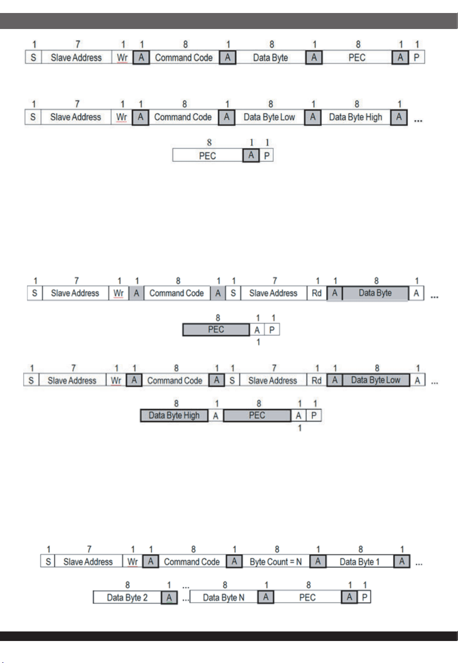
3.6.4.Write byte/word
The first byte of a Write Byte/Word access is the command code. The next one or
two bytes, respectively, are the data to be written. In this example, the master
asserts the slave device address followed by the write bit. The device acknowl-
edges and the master delivers the command code. The slave again acknowledg-
es before the master sends the data byte or word (low byte first). The slave
acknowledges each byte, and the entire transaction is finished with a STOP
condition.
16
Figure 5 –Write byte protocol with PEC
Figure 6 –Write Word Protocol with PEC
Figure 8–Read word protocol with PEC
Figure 9 –Block Write with PEC
Read byte/word
Reading data is slightly more complicated than writing data. First, the host must
write a command to the slave device. Then it must follow that command with a
repeated START condition to denote a read from that device’s address. The slave
then returns one or two bytes of data.
Note that there is no STOP condition before the repeated START condition, and
that a NACK signifies the end of the read transfer.
3.6.5.Block write/read
The Block Write begins with a slave address and a write condition. After the
command code, the host issues a byte count which describes how many more
bytes will follow in the message. If a slave has 20 bytes to send, the byte count
field will have the value 20 (14h), followed by the 20 bytes of data. The byte count
does not include the PEC byte. The byte count may not be 0. A Block Read or
Write is allowed to transfer a maximum of 32 data bytes.
y
Figure 7 –Read byte protocol with PEC
17
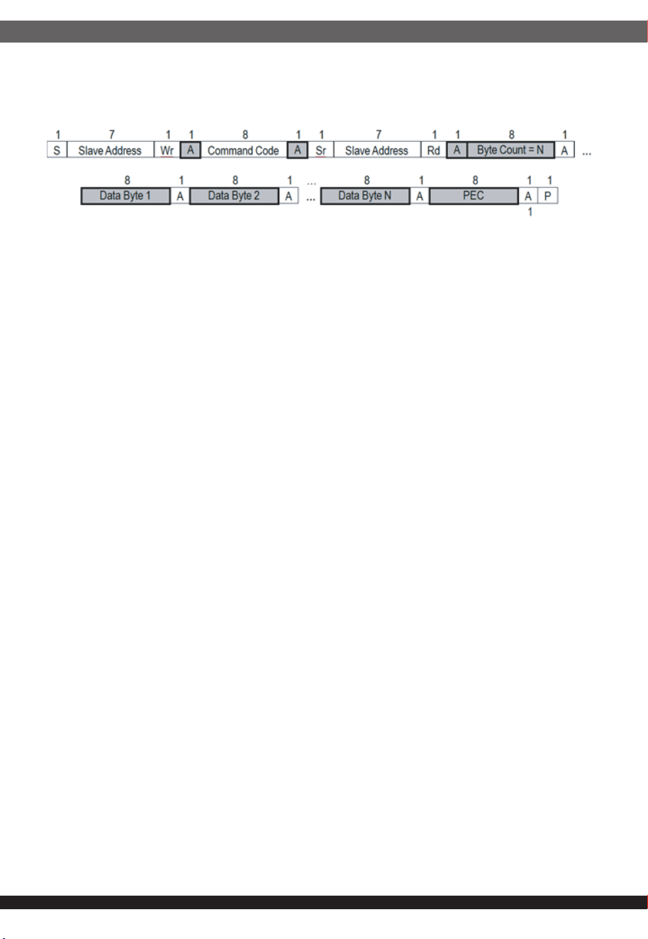
Figure 10 –Block Read with PEC
A Block Read differs from a block write in that the repeated START condition
exists to satisfy the requirement for a change in the transfer direction. A NACK
immediately preceding the STOP condition signifies the end of the read transfer.
4.ENVIRONMENTAL
The power supply shall operate normally, and sustain no damage as a result of
the environmental conditions listed in this chapter.
4.1.Temperature
Operating Ambient, normal mode (inlet Air): -5°C min/+50°C max at 5000m above
sea level.
(At full load, with a maximum rate of change of 5°C/10 minutes, but no more than
10°C/hr)
Operating Ambient, stand-by mode (inlet Air): -5°C min/+50°C max at 5000m
above sea level.
Non-operating ambient: -40°C to +70°C (Maximum rate of change shall be
20°C/hr)
4.2.Humidity
Operating: 5%- 85% relative humidity (non-condensing)
Non-operating: 5%- 95% relative humidity (non-condensing)
Note: 95% relative humidity is achieved with a dry bulb temperature of 55°C and a
wet bulb temperature of 54°C.
4.3.Altitude
A)Operation : sea level to 5000m
B)Non-Operation : sea level to 15,200m
4.4.Vibration
A)Operation : 0.01g²/Hz at 5 Hz sloping to 0.02g²/Hz at 20 Hz, and maintaining
0.02g²/Hz from 20 Hz to 500 Hz. The area under the PSD curve is 3.13gRMS.
The duration shall be 20 minutes per axis for all three axes on all samples.
B)Non-Operation :
-Sine sweep: 5Hz to 500Hz @ 0.5gRMS at 0.5 octave/min; dwell 15min at each of
3 resonant points;
4.5.Mechanical Shock
A)Operation: 10G, 4.3 mSec, no malfunction
B)Non-operating: 50G Trapezoidal Wave, Velocity change = 4.3m/sec. Three
drops in each of six directions are applied to each of the samples.

18
4.6Thermal shock (Shipping)
Non-operating: -40°C to +70°C, 50 cycles, 30°C/min. ≥ transition time ≥
15°C/min., duration of exposure to temperature extremes for each half cycle shall
be 30minutes.
4.7Catastrophic Failure
The power supply shall be designed to fail without startling noise or excessive
smoke.
4.8EMI
The power supply shall comply with FCC part 15, CISPR 32 and EN 55032; Class
A for both conducted and radiated emissions with a 6dB margin. Test shall be
conducted using a shielded DC output cable to a shielded load. The load shall be
adjusted to 100% load. Test will be performed at 115VAC @ 60Hz and 230VAC
@ 50Hz power input or -48VDC input.
The power supply shall comply with EN 55035.
The power supply when installed in the system must meet the following all the
immunity requirements when integrated into the end system.
5.REGULATORY Requirements
Intended Application – This product was evaluated as Information Technology
Equipment (ITE), which may be installed in offices, schools, computer rooms, and
similar commercial type locations. The suitability of this product for other product
categories and environments (such as: medical, industrial, telecommunications,
NEBS, residential, alarm systems, test equipment, etc.) other than ITE applica-
tion, may require further evaluation.
5.1Product Safety Compliance (Refer to Power Module)
A)UL/CUL (UL 62368-1)
B)TUV(EN 62368-1)
C)CB(IEC 62368-1)
D)CE
E)FCC
5.2Product EMC Compliance – Class A Compliance
The product is required to comply with Class A emission, as the system it is built
into might be configured with the intend for commercial environment or home use.
The Power supply is to have a minimum of 6dB margin to Class A Limits.

19
A)CISPR 32 – Emission
B)EN 55032 – Emission
C)EN 55035 – Immunity
-EN 61000-4-2 Electrostatic Discharges(ESD)
-EN 61000-4-3 Radio Frequency Electromagnetic Field(RS)
-EN 61000-4-4 Fast Transients Common Mode(EFT)
-EN 61000-4-5 Surges
-EN 61000-4-6 Radio Frequency Common Mode(CS)
-EN 61000-4-8 Power Frequency Magnetic Field (PFMF)
-EN 61000-4-11 Voltage Dips and Interruptions(DIP)
D)EN 61000-3-2 – Harmonics Current Measurement
E)EN 61000-3-3 – Voltage Fluctuations and Flicker Measurement
5.3Maximum AC Leakage current to ground (For AC Input)
3.5mA max for each power supply at 264Vac.
5.3.1 Hi-pot
The power supply module in the system shall be test at 1800Vac, with a trigger
limit of 30mA.
5.4Electrostatic Discharge (ESD)
In addition to EN 61000-4-2, the following ESD tests shall be conducted. Each
surface area of the system under test shall be subjected to twenty (20) successive
static discharges, at each of the following voltages: 15kV.
Performance criteria:
a)All power system output shall continue to operate within the limits of this specifi-
cation, without glitches or interruption, while the supply is operated as defined and
subjected to 2kV through 15kV ESD pulses. The direct ESD event shall not cause
any out of regulation condition. The power system shall withstand these tests
without nuisance trips.
b)The power system, while operating as defined, shall not have a component
failure when subjected to any discharge voltages up to and including 15kV.
Component failure is defined as any malfunction of the power supply caused by
component degradation or failure requiring component replacement to correct the
problem.
5.5Mean Time between Failures (MTBF)
The power supply shall have a minimum MTBF at continuous operation of
200,000 hours calculated at 100%, according to BELL CORE TR-322 at 25°C
excluding the Fan MTBF, and at least 100,000 hours including the fan MTBF.
20
⚎њֱ䅋Փ⫼㗙ঞ䰆☿ⱘⳂⱘˈᅝ㺱ℸѸᓣ䳏⑤կឝ఼ᰖˈᖙ䷜ᅝ㺱ᮐヺড়ϟ߫䷙㽕∖ⱘ←Ёˈ
ϺϨᅝ㺱ཹᕠˈᠡৃϞ䳏⑤DŽ
←ᴤ䊾䷜⚎䰆☿←DŽᴤ䋼乏Ў䰆☿DŽ
←ⱘϞᮍঞو䙞П೧ᔶ䭟ᄨˈ᳔ܻᕥϡৃᮐPPDŽ
←ⱘϞᮍঞو䙞П䭋ṱൟ䭟ᄨˈᇡ㾦㎮䎱䲶ϡৃᮐPP˗㢹ᇀᑺᇣᮐPPˈࠛ䭋ᑺϡফ䰤ࠊDŽ
←ᑩ䚼ϡৃ᳝䭟ᄨDŽᑩ䚼ϡৃ᳝ᓔᄨDŽ
ⳈᕥϡᮐPP
ᇡ㾦㎮ϡᮐPP
ᇀᑺᇣᮐPPࠛ䭋ᑺϡ䰤
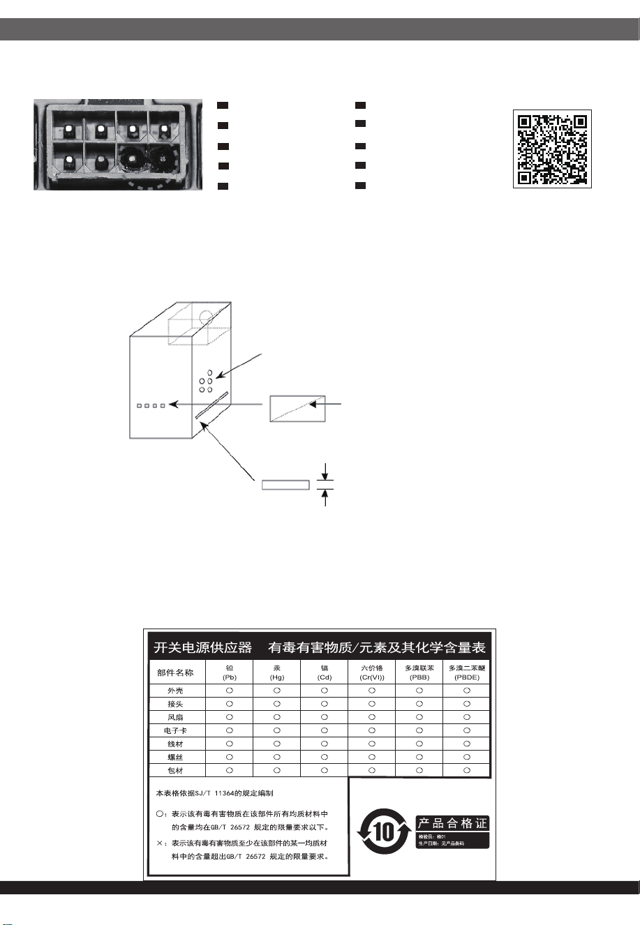
Openings that do not exceed 1mm in width regardless of length
Openings that do not exceed 5mm in any dimension
ᴀ⫶ક䔌ߎ᳝䱾㛑䞣ˈ⚎䙓ܡ᪡ᰖⱐ⫳䱾ˈ䷜ᮐ㺱ܹ㋏㍅″←Ϻᇛ᠔᳝䀁٭ᅝ㺱ཹ⭊ᕠᠡৃ䭟ଳ䳏⑤DŽ
ᴀ⫶કП䳏⑤䔌ߎ䴲ቀ䳏䰤ࠊൟ䳏⑤ˈ䂟䗷Փ⫼䰆☿←П䙞ˈҹ䙓ܡ☿♑䱾ⱐ⫳DŽ
%60,52+6䊛㿞
KWWSZZZVLOYHUVWRQHWHNFRPGRZQORDGV36856'SGI
6. Power Supply Connector Overuse Definition
Definition einer Überlastung des
Netzanschlusses
DE
Définition de l'utilisation excessive du
connecteur d'alimentation électrique
FR
Definizione di uso eccessivo del connettore
di alimentazione
IT
Definición de uso excesivo del conector de
la Fuente de alimentación
ES
Определение чрезмерной нагрузки на
коннектор блока питания
RU
電力供給コネクタの使用限度超過に関する説明
JP
⬉⑤կᑨ఼༈䖛ᑺՓ⫼ᅮН
CN
䳏⑤կឝ఼丁䘢ᑺՓ⫼ᅮ㕽
TW
ขีดจำกัดการรองรับการใช้งานของขั้วต่อจากพาวเวอร์ซัพพลาย
TH
전원 공급 커넥터 과용 정의
KR

21
This device complies with Part 15 of the FCC Rules.
Operation is subject to the following two conditions:
(1) this device may not cause harmful interference, and
(2) this device must accept any interference received,
including interference that may cause undesired operation.
Please refer to SilverStone website for latest specifications updates.
The equipment a Class | Switching Power Supply intended to use
for information technology equipment or Audio and Video equipment.
※付属の電源コードは当該製品専用です。他の機器に使用しないでください。
Model (safety certification): SST-CM2000GFTI-A
SST-CM2400GFTI-A
本製品は2000W;2400Wの出力が可能な高出力電源となります。
・一般家庭のコンセント(1500W)の場合は、1300W未満の消費電力でご利用ください。
・日本国内向けに販売されている本製品の付属電源ケーブルは100V(最大15A)専用となります。
・本製品に200V用電源ケーブル、および100V/20A用電源ケーブルの同梱はございません。
・100V/15A以外の環境でご利用の際は、安全の為、必要な電源ケーブルを別途ご用意ください。