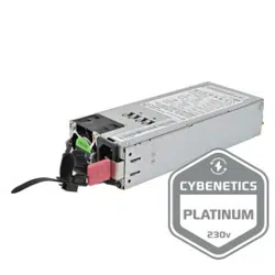

Gemini 1300C Platinum Module
Gemini Series
1300W Replacement Module
for Gemini 1300C Platinum (SST-GM1300C-PF)
●Replacement module for SilverStone Gemini 1300C Platinum (SST-GM1300C-PF)
●1U height CRPS form factor
●Full range Active PFC with Cybenetics Platinum certification
●All Japanese electrolytic capacitors
●Support PMBus 1.2
●Hot-swappable design with convenient pull-out handle bars
●Cold Redundancy
●Smart Ride Through (SmaRT) effectively obtains SMBAlert signal ensures continuity
of power during power instability and interruptions.
●Closed Loop System Protection (CLST)
●12V main output & 12V standby output
●3A max standby output current

SPECIFICATION
SilverStone Gemini Series
Gemini 1300C Platinum Module
SST-GM1300C-PFU
CRPS Module AC to DC Power Supply
Cybenetics Platinum efficiency certified.
01
1.General Description
GM1300C-PFU an AC/DC power supply with an input voltage range of
90~264Vac, 2 output voltages, main output 12.2V, standby output 12.2V,
maximum output power 1300W. The power supply has input over-under
voltage, output over-current, output over-voltage, short circuit, over-temperature
and other protection functions. At the same time, the power module can control
and monitor various functions through the I2C interface.
1.1 Function briefly
Model Output(V) Input(A)
SST-GM1300C-PFU
12.2V 2-105.3A
12.2V 0.5-3A
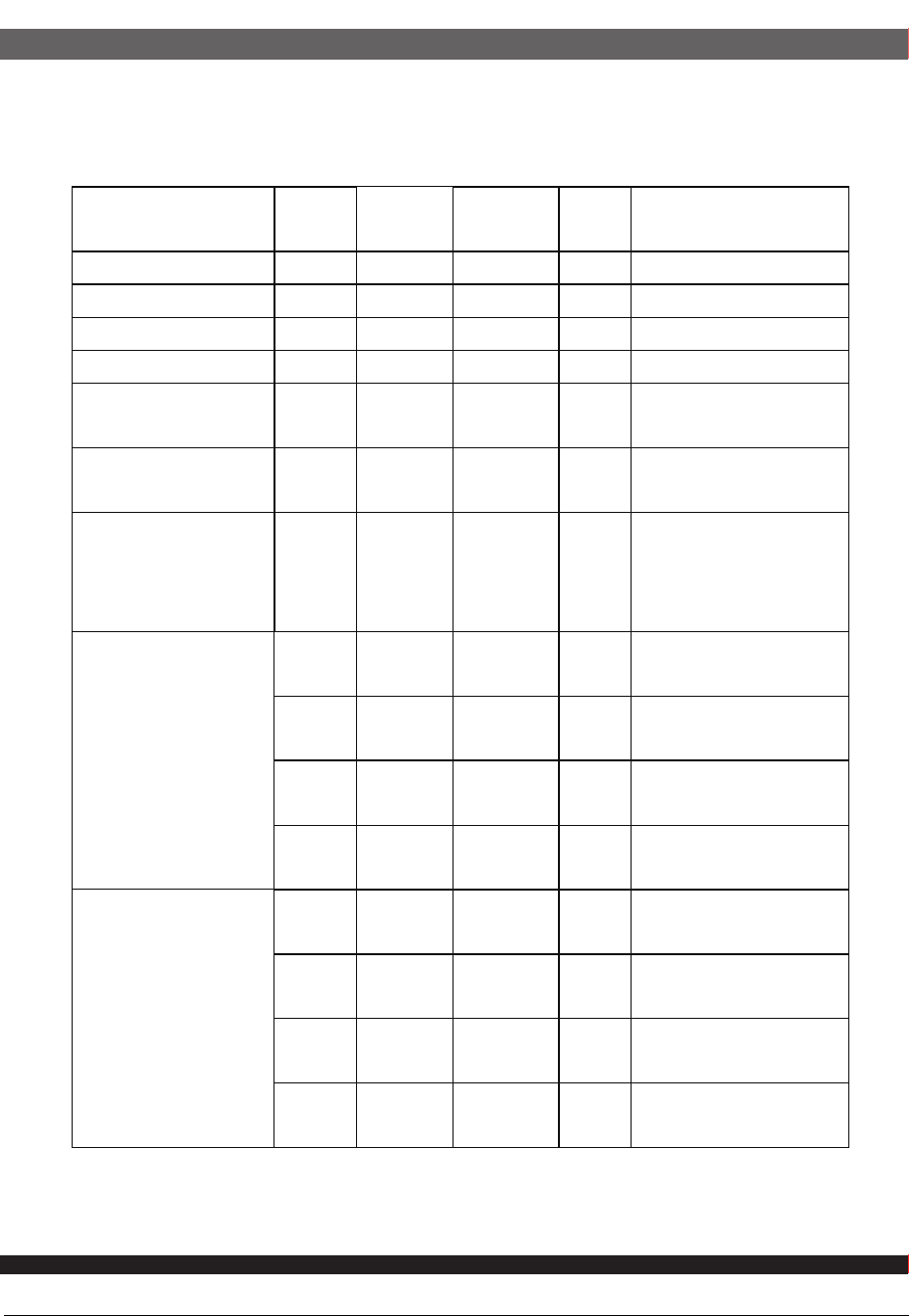
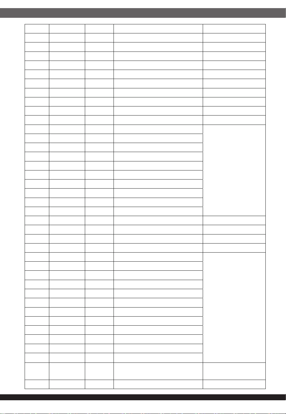
2.1.1 AC input requirements
2.Input requirements
02
item
meas
ure
Minimu
m
Nominal
Max
imum
note
Input Voltage Vac 90 115/230
264
Nom Input Voltage Vac 100 115/230
240
Vin Frequency Hz 47 50/60 63
Nom Vin Frequency Vdc 180 310
Nominal DC input
voltage range
Vdc 240
Maximum input
current
A / / 14
@90Vac 100% load
Input surge current
A / / 50
230Vac/50Hz input,
full load,cold start,
25℃
Power factor
0.9
10% load,230Vac,
50Hz& 115Vac,60Hz
0.96
20% load,230Vac,
50Hz& 115Vac,60Hz
0.98
50% load,230Vac,
50Hz& 115Vac,60Hz
0.99
100% load,230Vac,
50Hz& 115Vac,60Hz
iTHD
% 20
>10%&<20% load,
230Vac,50Hz
% 15
≥20% load,230Vac,
50Hz
% 10
≥40% load,230Vac,
50Hz
% 8
≥50% load,
230Vac,50Hz

03
2.1.2 Input protection function
Item measur
e
Minimum Nominal Maximum note
Input Over current
protection
A
/ / /
Yes, the input
fuse will blow
when
overcurrent
occurs.
Input under voltage
protection
Protect
point
/ /
82Vac
Full load test,
hysteresis more
than 5V.
Recover
point
/ /
88Vac
Input over voltage
protection
Protect
point
290Vac / /
Full load test,
hysteresis more
than 5V.
Recover
point
280Vac / /
04
3.Output requirements
3.1.1 AC output requirements
Item Unit MIN
Nomina
l
MAX Note
Output wattage W
1000W
90-140Vac
1300W
180-264Vac
Rated output voltage
V 11.6 12.2 12.8 Main output
V 11.6 12.2 12.8 Standby output
Rated output current
A 2 80.5 @90-140Vac
A 2 105.3 @180-264Vac
A 0.5 3 Standby
Range
%
±5
Main Output
% ±5
Standby
Delay turn on
ms 2500
Main output
ms 1500
Standby output
Raise time
ms 70 Main output
ms 70
Standby output
Hold up time ms 12
70%load,@230Vac
Ripple noise
mV 120
Main output(Ripple
noise test with
external 2200uF
solid capacitor
The
oscilloscope
has a
bandwidth of
20M, and the
output
terminal is
connected
with a 10UF
electrolytic
capacitor and
a 0.1UF
ceramic
capacitor.
mV 120
Standby output
(Ripple noise test
with external 270uF
solid capacitor)
Efficiency
% 92
20%load,@230Vac,fan with
external power supply.
% 94
50% load,@230Vac,fan with
external power supply.
% 91
100% load,@230Vac,fan with
external power supply.
Dynamic response
V
11.6 12.8
The dynamic load range is not
greater than 60%, the minimum load
is 3A, 0.5A/us. (Dynamic load
us 500
05
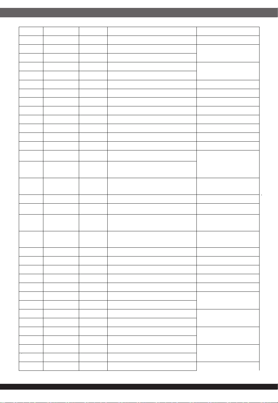
3.2.2 Output power characteristics
3.2.3 Output protection function
Output
Input
voltage
(Vac
)
Mi
n(
A)
Max(Lo
ng-term
load)
Peak load
capacity
(20s)(A)
Peak load
capacity
(10ms)(A)
Peak load
capacity
(100us)(A)
Main
output
180-
264
2
105.3
105.3+10
105.3+72
105.3+105
Main
output
90-140
2
80.5
80.5+10
80.5+72
80.5+105
Standby
output
90-264
0.5
3
>4
Item Unit MIN
Nomina
l
MAX Note
Main output Over
Current Protection
A
110 145
180-264Vac, hiccup, self-recovery
A
90 100
90-140Vac, hiccup, self-recovery
Standby A 4 9 hiccup, self-recovery
Main output short
circuit protection
/ / / /
Standby output, the main circuit can
recover automatically after the short
circuit is removed.
Standby output short
circuit protection
/
The main circuit has no output, and
the Standby can recover
automatically after the short circuit is
removed.
Over voltage
protection
Main V 13.5 15.5
The output is locked and the
Standby output is not turned off.
Seco
nd
V 13.5 15.5
Standby locks, turning off the main
output
Over temperature
protection
℃
60
Turn off the main circuit, it can self-
recovery, the hysteresis is not less
than 5℃, do not turn off the 3.3V
Standby.

3.2.4 Indicator
Note: The light is a two-color LED light
06
Condition Light condition note
The power supply is working normally (both 12V
& 12VSB are normal)
GREEN /
Power supply without AC input (including parallel
redundant power supplies)
OFF /
AC input is normal, 12VSB is normal, and 12V
has no output.
1Hz Blink GREEN Standby condition
No AC input, but the AC input of the parallel
redundant power supply is normal.
RED /
Power supply warning, such as over
temperature, over power, over current, fan
failure, etc.
1Hz Blink RED Output normally
Power supply protection, such as over -current
protection, over -voltage protection, over -
temperature protection, fan failure, input over -
and under-voltage protection, etc.
RED Fail or output protect
Power supply enters cold redundancy state
0.33Hz Blink
GREEN
1s OFF;2s GREEN
07
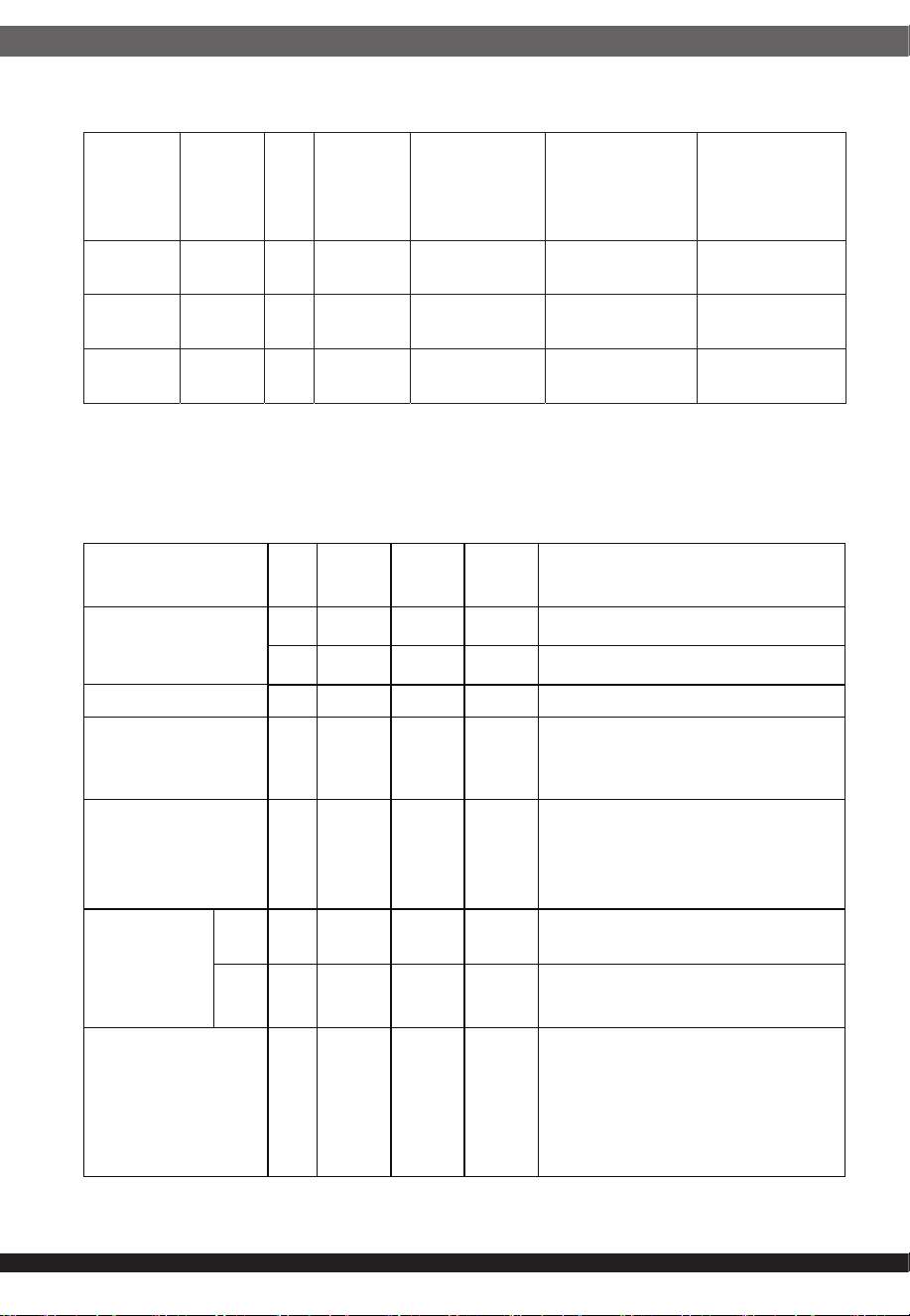
3.2.5 Timing
Item Description MI N MA X UNITS
T_vout_rise
Output voltage rise time for +12V and +12VSB
from 10% to within regulation limits.
70 ms
T_vstby_on_delay
Delay from AC being applied to +12VSB being
within regulation.
1500 ms
T_vin_on_delay
Delay from AC being applied to all output voltages
being within regulation.
2500 ms
T_vout_holdup
Time AC. +12V output voltage stay within
regulation after loss of
12 ms
T_psok_holdup Delay from loss of AC to de-assertion of PSOK. 10 ms
T_ps_on#_off_delay
Delay from PS_ON# de-asserted to power supply
turning off.
10 ms
T_ps_on#_on_delay
Delay from PS_ON# active to output voltages
within regulation limits.
5 400 ms
T_ps_on#_psok
Delay from PS_ON# deactivate to PSOK being de-
asserted.
5 ms
T_psok_on
Delay from output voltages within regulation limits
to PSOK asserted at turn on.
100 500 ms
T_psok_off
Delay from PSOK de-asserted to output voltages
dropping out of regulation limits.
1 ms
T_psok_low
Duration of PSOK being in the de-asserted state
during an off/on cycle using AC or the PS_ON#
signal.
100 ms
T_vstby_vout
Delay from +12VSB being in regulation to O/Ps
being in regulation at AC turn on.
50 1000 ms
T_vstby_holdup
Time the +12VSB output voltage stays within
regulation after loss of AC.
70 ms
Tvingood_de-assert
ed
Delay from the Vin drop being 0V to VIN_GOOD
de-assertion. (and SMBAlert# low)
3 ms
08
The redundant backup power supplies actively share current with each other
through the current sharing bus, and the current sharing strategy is average
current sharing. If one of the redundant backup power supplies fails, the operation
and output of other power supplies can’t be affected. Even if the current sharing
bus of a single power supply is short-circuit to ground, the power supply output
should still meet the specification requirements.
When the main circuit load of the power supply is greater than or equal to
50% of the rated power, the current average index should meet 6.5% (max).
When the main circuit load of the power supply is 20% and 30% of the rated load,
the current sharing unbalance is tested at two points, and it meets the require-
ment of not exceeding 10%;
4.1 Module test
1、Add 120% of the maximum design voltage of the bus to the current-sharing
bus and measure the output voltage variation. It is required that this value does
not exceed the output voltage regulation accuracy range of the rectifier module.
2、The current sharing requirements are as follows, 12Vsb is no-load during
testing.
4.Load sharing performance requirements

09
4.2 Turn on test
1. Under all input voltage and output current combinations, the output ripple must
not have low-frequency oscillation;
2. Under various cross loads and input voltages, when plugging or unplugging
any power supply, the overshoot (including undershoot) on the output DC bus
must meet the specification requirements;
3. Dynamically respond to the output voltage under various extreme conditions to
meet the system output voltage stabilization accuracy requirements;
4. When starting up under pure resistive load conditions of 0%, 25%, 50%, 75%
and 100%, the system output voltage power-on waveform must be smooth;
5. Repeatedly plug and pull modules, and the power system must not cause other
modules to die due to plugging and pulling;
6. Switching, plugging and unplugging the power supply must not cause abnor-
mality in the output signal of the relevant power supply;
7. The power module should be able to support up to 4 power supplies in parallel
for current sharing;
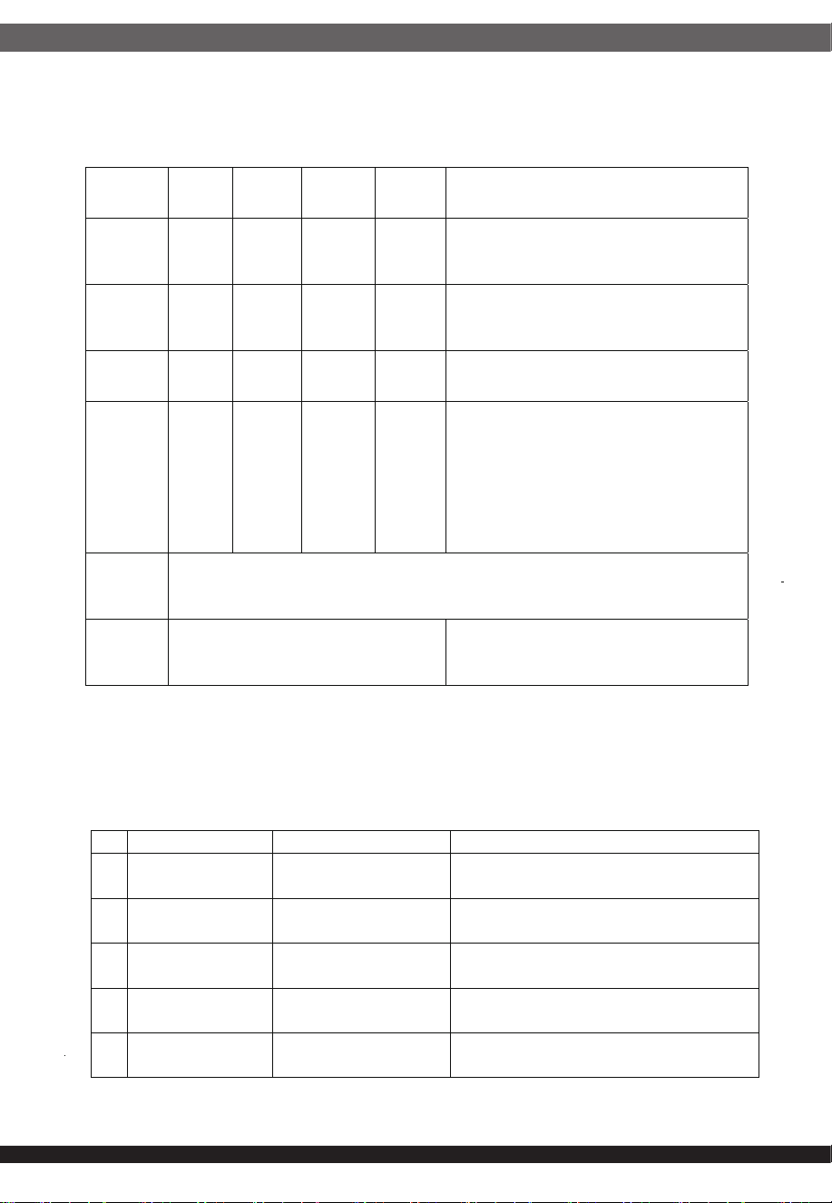
5.1 Cold redundancy configuration
There is a register Cold Redundancy configuration (D0h) inside the power supply,
which can be read or written accessed by the system. An example of the com-
mand format, such as S B0 w D0 01 PEC P means to set the D0h address
register value in power supply B0 to 01h. The register value can be set to
00h/01h/02h/03h/04h as needed. The meanings represented by different values
are describe in the following table:
5. Cold redundancy requirement
Value
State
Description
Active
Stop
00h
Standard
Redundancy
Power load sharing
redundant backup
operation
01h
Cold Redundant
Active
Power supply with
normal operating
output power in cold
backup
10
02h
Cold Standby 1
The first power supply
to exit cold backup
and enter working
status
40% of max
0.9 x(40% of
max x 1/2)
=18%
03h
Cold Standby 2
The second power
supply exits the cold
backup and enters the
working state
62% of max
0.9 x(62% of
max x 2/3)
=37.2%
04h
Cold Standby 3
The third power
supply exits the cold
backup and enters the
working state
84% of max
0.9 x(84% of
max x 3/4)
=56.7%
Note: The factory default state of the power supply is Standard Redundancy, and
the corresponding D0h register value is 00h.
5.2 PSU turn on function
The power on and off power supply in cold backup is only controlled by the output
load. Once the load exceeds the enable threshold, the power supply is turned on;
when the load decreases to the disable threshold, the power supply enters Cold
standby.

11
5.3 Cold Standby work condition
5.4Turn on smart opening function
The necessary conditions for the power supply to enter the Cold standby
state are: PSON low level and the register value is 02h/03h/04h. At the
same time, for the power supply that enters the Cold standby state, the
requirements are:
• When CRB is low, the power supply in Cold Redundant Active and Cold
Standby should be able to wake up immediately and the D0h value returns
to 00h, entering the standard redundancy state.
• Keep PWOK high
• All states of the power supply should remain normal, and no faults or
abnormalities should be reported unless a fault or abnormality does occur.
• The indicator light flashes according to the specifications.
• All fans remain running
• LED flashes green
• Any time any power supply is abnormal, pull down the CRB level, and all
power supplies will automatically enter the Standard Redundancy state.
The CRB low level range is 0V-0.6V; the high level range is 2.0V-3.46V,
and the timing priority of CRB pulling down must be High to ensure timely
wake-up of other Cold Redundant power supplies.
The cold redundancy power supply must exit the cold backup state under
fault or overcurrent conditions
Any abnormality in the power supply will restore the register value to the
default value 00h, and set the Cold Redundant BUS abbreviation CRB
(B22 PIN) to low level, forcing other power supplies working in parallel to
enter the standard redundancy state. Trigger conditions:
1. A 12V OCP alarm failure occurs
2.12V OVP fault
3.12V UVP
4. OTP alarm failure
5. Fan speed alarm failure
6. AC power failure
Here are the steps to put your PSU into smart-on mode. PSUs designated
as smart standby can be powered off and on to main power when neces-
sary. For practical applications, the above trigger levels may have a
tolerance of +/-10%.
12
Step 1: Make sure each PSU has an AC power cord connected. Use the
Write Bytes command to set command 0xD0 for each PSU to have its own
role (there must be one PSU as the active role). The command format of
the smart enable function is as follows.
B0 is in smart on state (S B0 w D0 01 PEC P)
B2 is in smart on standby state (S B2 w D0 02 PEC P)
Step 2: Once the load drops below the corresponding trigger point, the
PSU will enter smart slave mode.
Step 3: If the CRB signal drops low, all PSUs will turn on main power and
reset Cold_Redundancy_CONFIG to 0x00. The system needs to reassign
the positions of all PSUs to enable the smart on feature again.
The power supply should support access to PMBUS information via the
I2C bus. The power supply is equipped with four pin connectors, namely
SCL, SDA, A1, and A0. Clock bus (SCL) and data bus (SDA), the two pins
communicate each other and form a continuous bus, A0 and A1 are used
to determine the address. The backplane defines the state of these lines
so that the power supply address is unique within the system. The gener-
ated I2C address should conform to the table below. The write protect pin
is used to ensure data is not lost due to accidental overwriting. The bus
operates at 3.3V voltage, and SDA and SCL need to be pulled up to 3.3V
on the system board.
6.PMBUS AND EEPROM
6.1 PMBUS
MCU Address
System addressing
PMBUS
IPMI FRU
A1
A0
PSU-1
B0
A0
0
0
PSU-2
B2
A2
0
1
PSU-3
B4
A4
1
0
PSU-4
B6
A6
1
1
The power supply can monitor and read the input voltage, input power, output voltage,
output current and other data of the power supply in real time.
CMD Code Name Type Bytes
Conditions
01h OPERATION Read/Write 1
Power on/off sign, 0x80
means power on (default
value), 0x00 means power off
02h ON_OFF_CONFIG Read/Write 1
0x15 (hardware controlled
power on and off, default
value), 0x19 (software
controlled power on and off)

13
03h CLEAR_FAULTS N/A 0
19h CAPABILITY Read Byte 1 Value 90h
1Ah QUERY
Block Write-
Block Read
Process Call
1
20h VOUT_MODE Read Byte 1
3Ah FAN_CONFIG_1_2 R/W 1 D0h
3Bh
FAN_COMMAND_1
R/W
2
79h STATUS_WORD Read Word 2
7Ah STATUS_VOUT Read Byte 1
7Bh STATUS_IOUT Read Byte 1
7Ch STATUS_INPUT Read Byte 1
7Dh STATUS_TEMPERATURE Read Byte 1
88h READ_VIN Read Word 2
8Bh READ_VOUT Read Word 2
8Ch READ_IOUT Read Word 2
8Dh READ_TEMPERATURE_1 Read Word 2
96h READ_POUT Read Word 2
97h READ_PIN Read Word 2
98h PMBUS_REVISION Read Byte 1 Value 22h
99h MFR_ID Read Block Variable
9Ah MFR_MODEL Read Block Variable
9Bh MFR_REVISION Read Block Variable
A0h MFR_VIN_MIN Read Word 2
A1h MFR_VIN_MAX Read Word 2
A2h MFR_IIN_MAX Read Word 2
A3h MFR_PIN_MAX Read Word 2
A4h MFR_VOUT_MIN Read Word 2
A5h MFR_VOUT_MAX Read Word 2
A6h MFR_IOUT_MAX Read Word 2
A7h MFR_POUT_MAX Read Word 2
A8h MFR_TAMBIENT_MAX Read Word 2
A9h MFR_TAMBIENT_MIN Read Word 2
ABh MFR_EFFICIENCY_HL Read Block 14
D0h Cold standby R/W 1
6.2 EEPROM
6.2.1 EEPROM Data
The EEPROM data format shall comply with the IPMI version 1.0 (document
revision 1.3 March 24, 2015) specification.
14
6.2.2 EEPROM data format
EEPROM Addressing
Item Address
Byte Value
(hex)
Description
Area
0 00H 01 Common Header Format Version Number
1 01H 00 Internal Use Area
2 02H 00 Chassis Info Area
3 03H 00 Board Info Area
4 04H 01 Product Info Area
5 05H 0C Multi Record Info Area
6 06H 00 PAD Area
7 07H F2 Common Header Checksum (Total Of Bytes)
8 08H 01
Product Area Format Version
Product Information Area
9 09H 0B Product Area Length
10 0AH 19 Language Code
11 0BH C9 Manufacturer Name type/length byte
12
0CH 46
Manufacturer Name bytes
13
0DH
53 Manufacturer Name bytes
14
0EH
50 Manufacturer Name bytes
15
0FH
20 Manufacturer Name bytes
16
10H
47 Manufacturer Name bytes
17
11H
52 Manufacturer Name bytes
18
12H
4F Manufacturer Name bytes
19
13H
55 Manufacturer Name bytes
20
14H
50 Manufacturer Name bytes
21
15H
CD Product Name type/length byte
22
16H
46 Product Name bytes
23
17H
53 Product Name bytes
24
18H
50 Product Name bytes
25
19H
31 Product Name bytes
15
26
1AH
33 Product Name bytes
27
1BH
30 Product Name bytes
28
1CH
30 Product Name bytes
29
1DH
2D Product Name bytes
30
1EH
32 Product Name bytes
31
1FH
51 Product Name bytes
32
20H
30 Product Name bytes
33
21H
31 Product Name bytes
34
22H
41 Product Name bytes
35
23H
31 Product Name bytes
36 24H
Product Part/Model Number type/length byte
37 25H
Product Part Number bytes Need be consistent with SPEC
label
38
26H
Product Part Number bytes
39
27H
Product Part Number bytes
40 28H
Product Part Number bytes
41 29H
Product Part Number bytes
42 2AH
Product Part Number bytes
43 2BH
Product Part Number bytes
44
2CH
Product Part Number bytes
45 2DH
Product Part Number bytes
46
2EH
Product Part Number bytes
47 2FH
C2 Product Version type/length byte
48 30H
Product Version Need be consistent with BOM
49 31H
Product Version
50 32H
Product Serial Number type/length byte
51 33H
Product Serial Number bytes Need be consistent with SPEC
label
52 34H
Product Serial Number bytes
53 35H
Product Serial Number bytes
54 36H
Product Serial Number bytes
55 37H
Product Serial Number bytes
56
38H
Product Serial Number bytes
57 39H
Product Serial Number bytes
58 3AH
Product Serial Number bytes
59 3BH
Product Serial Number bytes
60 3CH
Product Serial Number bytes
61
3DH
Product Serial Number bytes
62
3EH
Product Serial Number bytes
63
3FH
C1 type/length byte encoded to indicate no more
info fields
64
40H 00
PAD

16
65
41H 00
PAD
66
42H 00
PAD
67
43H 00
PAD
68
44H 00
PAD
69
45H 00
PAD
70
46H 00
PAD
71
47H 00
PAD
72
48H 00
PAD
73
49H 00
PAD
74
4AH 00
PAD
75
4BH 00
PAD
76
4CH 00
PAD
77
4DH 00
PAD
78
4EH 00
PAD
79
4FH 00
PAD
80
50H 00
PAD
81
51H 00
PAD
82
52H 00
PAD
83
53H 00
PAD
84
54H 00
PAD
85 55H 00
PAD
86 56H 00
PAD
87
57H 00
PAD
88
58H 00
PAD
89 59H 00
PAD
90 5AH 00
PAD
91 5BH 00
PAD
92 5CH 00
PAD
93
5DH
00
PAD
94 5EH 00
PAD
95
5FH
Product Info Area Checksum Sum Of Byte8 ~95
96 60H 00
Record Type ID Power Supply Information
97 61H 02
End of List/Record Format Version
98 62H 18
Record Length
99 63H
Record Checksum (zero checksum)
100 64H
Header Checksum (zero checksum)
101 65H 14
Overall Capacity in Watts (LSB) 1300W
102 66H 05
Overall Capacity in Watts (MSB)
103 67H FF
104 68H
FF
Peak VA
17
105
69H 32
Inrush current 50A
106 6AH 05
Inrush interval in ms. 5ms
107 6BH 28
Low end Input voltage range 1 (10mV ,LSB) 90V
108 6CH 23
Low end Input voltage range 1 (10mV ,MSB)
109 6DH
20
High end Input voltage range 1 (10mV ,LSB) 264V
110
6EH
67 High end Input voltage range 1 (10mV ,MSB)
111
6FH
00 Low end Input voltage range 2 (10mV ,LSB)
112
70H
00 Low end Input voltage range 2 (10mV ,MSB)
113
71H
00 High end Input voltage range 2 (10mV ,LSB)
114
72H
00 High end Input voltage range 2 (10mV ,MSB)
115
73H
2F Low end Input frequency range 47Hz
116
74H
3F High end Input frequency range 63Hz
117
75H
0C
A/C dropout tolerance in ms(100%Load) 12mS
118
76H
1B Binary flags
119
77H
48
Peak Wattage(LSB)
1352W,15S
120
78H F5
Peak Wattage(MSB) – Hold up time in
seconds
121
79H
00
Combined Wattage
15S7:4 – Voltage 1;3:0 –
Voltage 2
122
7AH
00 Combined Wattage (LSB)
123
7BH
00
Combined Wattage (MSB)
124
7CH
00
Predictive fail tachometer lower threshold
(RPS)
125
7DH 09
Record Type ID (0x01: DC Output, 0x09:
Extended DC Output)
12V Output Record
126 7EH
02 End of List/Record Format Version
127
7FH
0D Record Length
128
80H
Record Checksum (zero checksum)
129 81H
Header Checksum (zero checksum)
130 82H
1 Output Information
131
83H
C4 Nominal voltage (10 mV) (LSB) 12.2V
132
84H
04 Nominal voltage (10 mV) (MSB)
133
85H
88 Maximum negative voltage (10 mV) (LSB) 11.6V
134
86H 04
Maximum negative voltage (10 mV) (MSB)
135 87H 00
Maximum positive voltage (10 mV) (LSB) 12.8V
136 88H 05
Maximum positive voltage (10 mV) (MSB)
137 89H 78
Ripple and Noise (1mV) (LSB) 120mV
138 8AH
00 Ripple and Noise (1mV) (MSB)
139
8BH
32 Minimum current draw (10mA) (LSB) 2A

18
140
8CH 00
Minimum current draw (10mA) (MSB)
141
8DH
22
Maximum current draw (10mA) (LSB)
105.3A
142 8EH
29 Maximum current draw (10mA) (MSB)
143
8FH
09 Record Type ID 12Vsb Output Record
144
90H 82
End of List/Record Format Version
145 91H 0D
Record Length
146 92H
Record Checksum (zero checksum)
147
93H
Header Checksum (zero checksum)
148 94H 82
Output Information
149 95H C4
Nominal voltage (10 mV) (LSB) 12.2V
150 96H 04
Nominal voltage (10 mV) (MSB)
151 97H 88
Maximum negative voltage (10 mV) (LSB) 11.6V
152 98H 04
Maximum negative voltage (10 mV) (MSB)
153 99H 00
Maximum positive voltage (10 mV) (LSB) 12.8V
154 9AH 05
Maximum positive voltage (10 mV) (MSB)
155 9BH 78
Ripple and Noise (1mV) (LSB) 120mV
156 9CH 00
Ripple and Noise (1mV) (MSB)
157 9DH
00
Minimum current draw (10mA) (LSB) 0.5A
158
9EH
00 Minimum current draw (10mA) (MSB)
159
9FH
2C Maximum current draw (10mA) (LSB) 3A
160
A0H
01 Maximum current draw (10mA) (MSB)
161
A1H
FF
162
A2H
FF
163
A3H
FF
164
A4H
FF
165
A5H
FF
166
A6H
FF
167
A7H
FF
168
A8H
FF
169
A9H
FF
170
AAH
FF
171
ABH
FF
172
ACH
FF
173
ADH
FF
174
AEH
FF
175
AFH
FF
176
B0H
FF
177
B1H
FF
178
B2H
FF
179
B3H
FF

19
180
B4H
FF
181
B5H
FF
182 B6H FF
183 B7H FF
184
B8H
FF
185
B9H
FF
186 BAH FF
187 BBH FF
188 BCH FF
189 BDH FF
190
BEH
FF
191 BFH FF
192
C0H
FF
193 C1H FF
194 C2H FF
195 C3H FF
196 C4H FF
197 C5H FF
198 C6H FF
199 C7H FF
200 C8H FF
201
C9H
FF
202
CAH
FF
203
CBH
FF
204 CCH FF
205 CDH FF
206 CEH FF
207
CFH
FF
208
D0H
FF
209
D1H
FF
210
D2H
FF
211
D3H
FF
212
D4H
FF
213
D5H
FF
214
D6H
FF
215
D7H
FF
216
D8H
FF
217
D9H
FF
218
DAH
FF
219
DBH
FF

20
220
DCH
FF
221
DDH
FF
222
DEH
FF
223
DFH
FF
224
E0H
FF
225
E1H
FF
226
E2H
FF
227
E3H
FF
228
E4H
FF
229
E5H
FF
230
E6H
FF
231 E7H FF
232 E8H FF
233
E9H
FF
234
EAH
FF
235 EBH FF
236 ECH FF
237 EDH FF
238 EEH FF
239 EFH FF
240 F0H FF
241 F1H FF
242 F2H FF
243 F3H FF
244 F4H FF
245 F5H FF
246 F6H FF
247 F7H FF
248 F8H FF
249 F9H FF
250 FAH FF
251 FBH FF
252 FCH FF
253 FDH FF
254 FEH FF
255 FFH FF
21
7.Environmental and reliability requirements
7.1 Environment
When the environment is 35℃ and 100% load, the mean time between failures
(MTBF) of the power supply is greater than 200,000 hours.
7.2 MTBF
7.3 Test environment requirement
Item Unit
MIN
NORMA
L
MAX
Item
Operating
temperat
ure
℃
0 25
55
100% load
Storage
temperat
ure
℃
-40
85
Storage
humidity
%
95 Not turn on the power and on the no
condensation.
Altitude m 0 / 5000
When the power supply works for a
long time, the maximum temperature at
sea level (the maximum temperature
defined in the specification book)
decreases by 0.33°C for every 100m
increase in altitude.
Heat
dissipatio
n method
The power supply comes with air cooling (exhaust air from the DC terminal
side to the AC input side)
Noise
58dB,@33℃,230Vac
Test method refers to ISO7779
bystander sound pressure level noise
test
No Test item Standard Note
1 Low Temperature
Work)
0℃
24h
2 High Temperature
Work)
55℃
24h
3 Low Temperature
Storage)
-40℃
24h
4 High Temperature
Storage)
85℃
24h
5 Temperature
Cycling
-5~55℃
Each cycle is 3 hours, high and low
temperature are 1 hour, 380 cycles
22
8 Safety requirement
9.EMC Requirement
8.1 Safety
8.2 Withstand voltage test and leakage current requirements
Standard Description
IEC 60950-1 ‘Information technology equipment – Safety. Part 1: General requirements’, plus all
existing national and group differences within the IECEE CB Scheme
GB 4943.1 Safety of Informa tion Technology Equipment (Including Electrical Busi ness
Equipment) (standard for China, equivalent to IEC 60950)
IEC 60664-1 Insulation coordination for equipment
within low-voltage systems -Part 1:Principles, requirements and tests
IEC62368-1 Audio/video, information and communication technology equipment -- Part 1: Safety
requirements
Test item Requirement
primary versus
secondary
The primary and secondary should be able to withstand 2545Vdc or 1800Vac for 1
minute, leakage current ≤20mA, and no breakdown or arcing.
Insulation
resistance
Under normal atmospheric pressure, relative humidity <90%, no condensation,
when the test voltage is 500VDC, the insulation resistance between primary and
secondary, primary and protective ground and secondary and protective ground is
≥10M
Leakage
current
<3.5mA,264Vac
Item Requirement Standard Note
(RE)
Frequency:30MHz~1GHz
Class A
EN 55022
230V@50Hz powered
FCC part 15
120V@60Hz powered
(CE)
Frequency:150KHz~30MHz
Class A
EN 55022
230V@50Hz powered
FCC part 15
120V@60Hz powered
(harmonic)
EN 61000-3-2 class A and Class D
requiremnet.
EN 61000-3-2 230V@50Hz powered
(Flicker)
Pst not higher then 1.0;
Plt value not over 0.65;
The relative voltage change dc does
not exceed 3.3%;
The maximum relative voltage change
dmax does not exceed 4%;
The time during which the d(t) value
exceeds 3.3% during voltage changes
shall not exceed 500ms.
EN 61000-3-3 230V@50Hz powered

23
Item Requirement Category Standard Note
SURGE
AC input:
Differential mode:±1KV,
Common mode:±2KV
B
EN61000-4-5
EN 55024
Basic requirement
EFT
AC input:±2KV
B
EN61000-4-4
EN 55024
YD/T 1082
ESD
contact discharge:±6KV
air discharge:±8KV
B
EN61000-4-2
EN 55024
RS
80M~800MHz 3V/m
800M~960MHz 10V/m
960M~1GHz 3V/m
1.4G~2GHz 10V/m
2G~2.7GHz 3V/m
80% AM
A EN 61000-4-3
CS
150KHz~80MHz
3V,80% AM
A
EN 61000-4-6
EN 55024
10. Dimension
73.5mm (W) x 40mm (H) x 185mm (D)
24
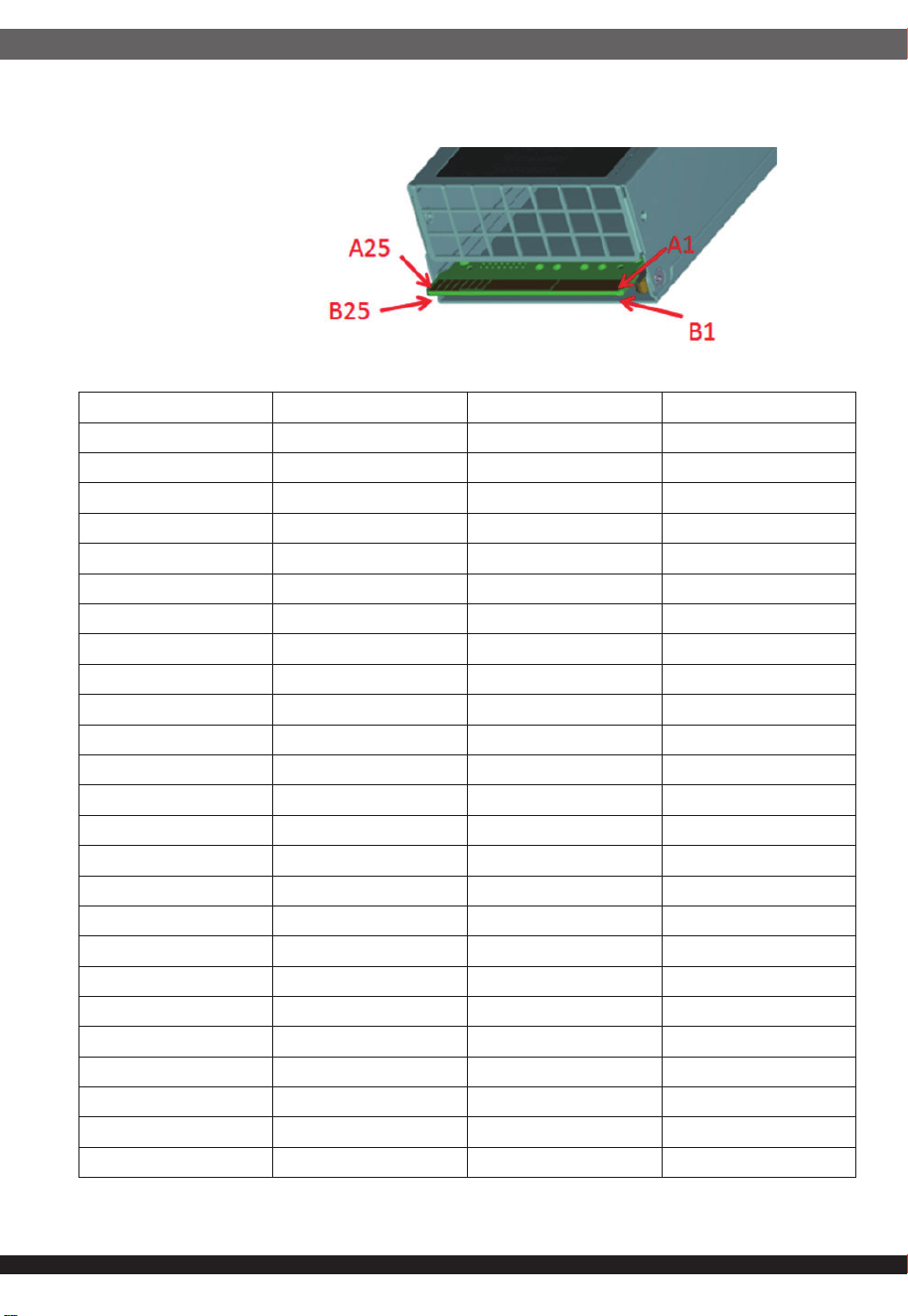
11.Pin Define
Pin Number
Definition
Pin Number
Definition
A1
GND
B1
GND
A2
GND
B2
GND
A3
GND
B3
GND
A4
GND
B4
GND
A5
GND
B5
GND
A6
GND
B6
GND
A7
GND
B7
GND
A8
GND
B8
GND
A9
GND
B9
GND
A10
+12V
B10
+12V
A11
+12V
B11
+12V
A12
+12V
B12
+12V
A13
+12V
B13
+12V
A14
+12V
B14
+12V
A15
+12V
B15
+12V
A16
+12V
B16
+12V
A17
+12V
B17
+12V
A18
+12V
B18
+12V
A19
SDA
B19
A0
A20
SCL
B20
A1
A21
PSON
B21
+12VSB
A22
SMB_ALERT
B22
CRB
A23
RETURN_SENSE
B23
SHARE
A24
REMOTE_SENSE
B24
PRESENT
A25
PWOK
B25
AC_FAIL