Copyright©
Shenzhen Minewsemi Co., Ltd.
Bluetooth LE Module
V 1.1.0
ME54BS62
Datasheet

02
ME54BS62
Datasheet
Version Note
Version Details Contributor(s) Date Notes
1.0.0 First edit Michelle 2026.01.27
Click the icon to view and download the latest product documents electronically.
https://en.minewsemi.com/file/ME54BS62-nRF54L15_Datasheet_K_EN.pdf
@
Part Number
Model Hardware Code
ME54BS62
1Y15TE
1.1.0 Updated PCB Design Michelle 2026.05.13
ME54BS62
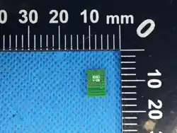
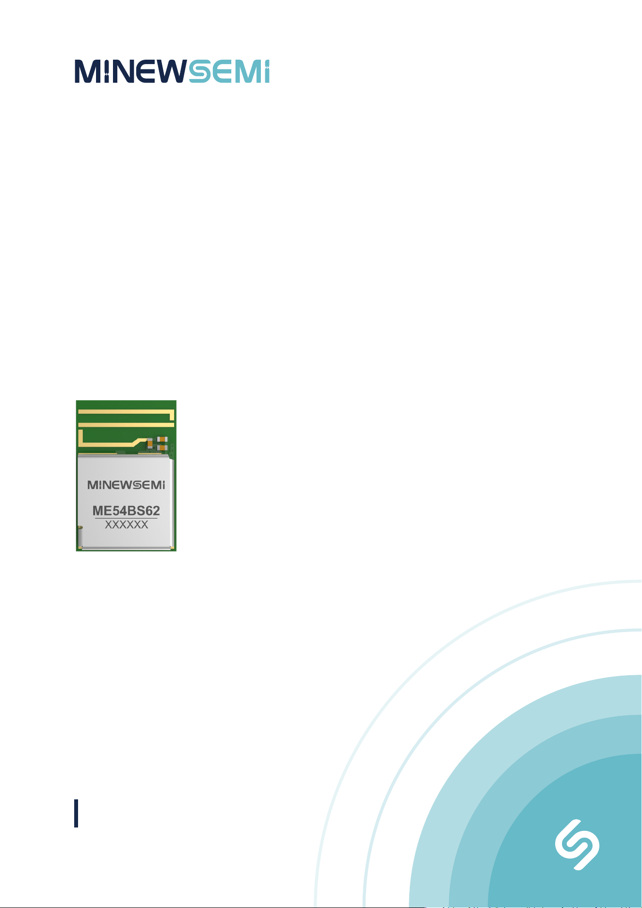
ME54BS62 is a highly flexible, ultra-low-power, cost-effective, and ultra-compact Bluetooth module based on the nRF54L15
WLCSP. Measuring just 6.0 × 9.0 × 1.8 mm, it is ideal for space-constrained designs. The module features a powerful Arm®
Cortex®-M33 processor running at up to 128 MHz, along with 1524KB NVM and 256 KB RAM to support advanced applica-
tion development.
Equipped with an integrated PCB antenna, the ME54BS62 enables reliable wireless connectivity while simplifying product
design and reducing external RF requirements. Leveraging the superior performance of the nRF54 series and offering abun-
dant GPIO resources, the module delivers excellent RF performance and energy efficiency, making it an ideal choice for
next-generation Bluetooth connectivity applications.
Ultra-Small Size, Ultra-Low Power, BLE 6.0 Supported Bluetooth
Module with PCB Antenna
Web:www.minewsemi.com Tel:0086 755-2801 0353 E-mail:minewsemi@minew.com Copyright© Shenzhen Minewsemi Co., Ltd.
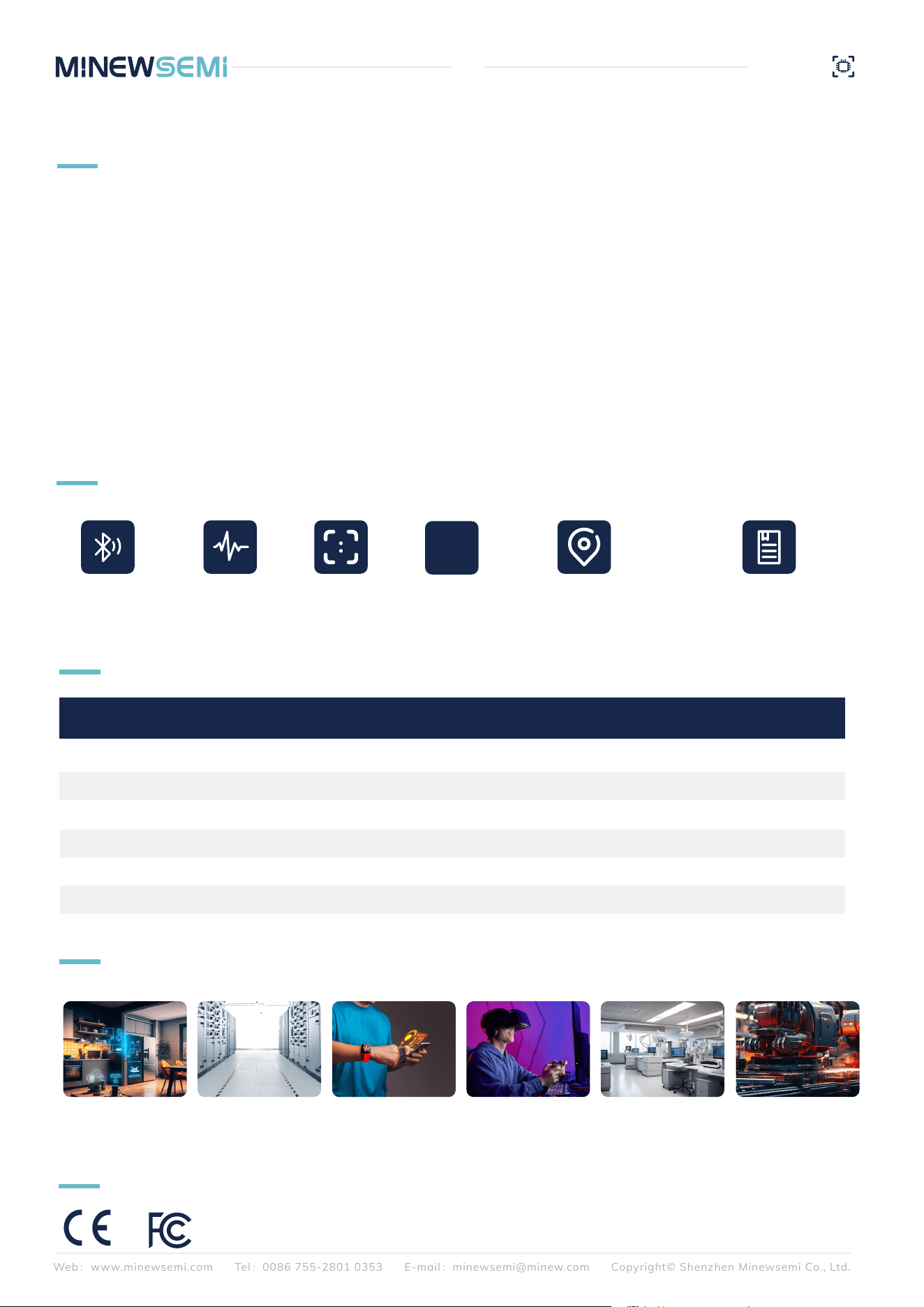
APPLICATION
Smart
Home
Computer
Accessories
Game controllers
and Remotes
Medical Devices Industrial IoT
Virtual reality and
Augmented reality
FEATURES
KEY PARAMETER
Chip Model
Module Size
Flash
Receiving Sensitivity
Emitting Current
Connection distance
nRF54L15
6.0×9.0×1.8mm
1524KB NVM
-96dBm
0dBm-5mA
10~70m
Antenna
GPIO
RAM
Transmission Power
Receiving Current
PCB
30
256 KB
-40 ~ +8dBm
3.2mA
ME54BS62
03
ME54BS62
Datasheet
Bluetooth 6.0 Ultra-low power
Multi-Protocol supports: Bluetooth LE 6.0
Channel Sounding, Bluetooth Mesh, Thread,
Matter, and proprietary 2.4 GHz protocols
Ultra-small size,
only 6*9mm size
Integrated PCB antenna with a
connectivity range of 10–70 meters
Support OTA
OTA
CERTIFICATION
11 Storage Conditions
12 Handling Conditions
INDEX
1 Block Diagram 05
2 Electrical Specification
05
3 Pin Description
06
4 Pin Definition
06
07
5 Mechanical Drawing
07
6 Electrical Schematic
08
7
PCB Design
10
8 Reflow and Soldering
11
9 Package Information
12
10 FCC warning
15
15
14 Copyright Statement
15 Related Documents
16
16
13 Quality
15
Web:www.minewsemi.com Tel:0086 755-2801 0353 E-mail:minewsemi@minew.com Copyright© Shenzhen Minewsemi Co., Ltd.
04
ME54BS62
Datasheet
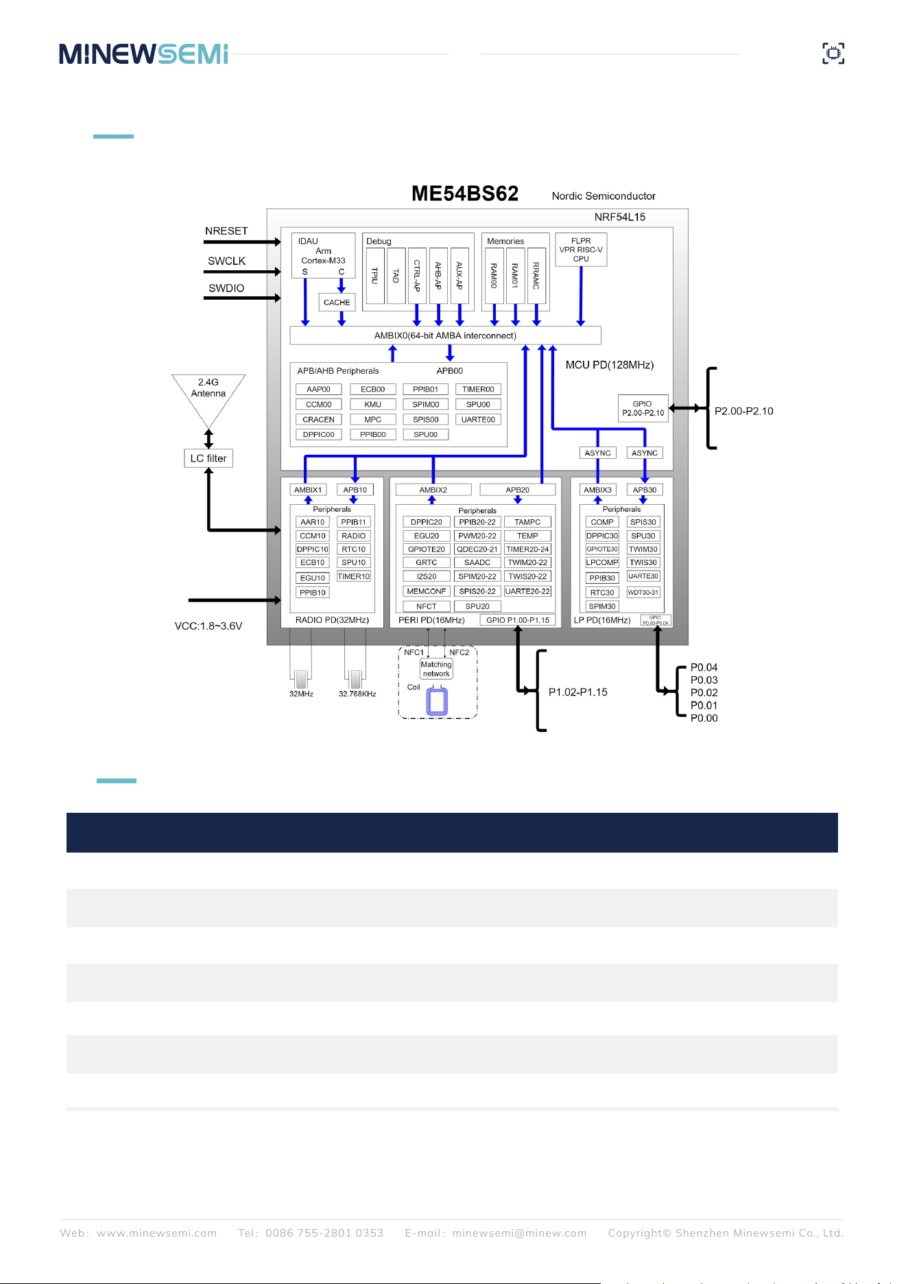
BLOCK DIAGRAM
1
2
ELECTRICAL SPECIFICATION
Working Voltage
Working Temperature
Transmission Power
Current(RX)
Current(TX)
Module Dimension
Quantity of IO Port
Operating temperature from -40°C to 105°C
Configurable
RF receiving current under 1Mbps pattern
RF transmission current under 0dBm pattern
1.7V-3.6V
-40℃~+105℃
-40 ~ +8dBm
3.2mA
5mA
6.0*9.0*1.8mm
30
Parameter Values Notes
Web:www.minewsemi.com Tel:0086 755-2801 0353 E-mail:minewsemi@minew.com Copyright© Shenzhen Minewsemi Co., Ltd.
05
ME54BS62
Datasheet
To ensure proper RF performance, it is recommended that
the supply voltage is not lower than 2.3V
3
4
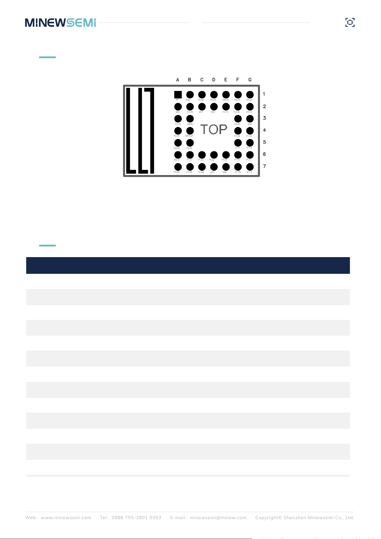
PIN DESCRIPTION
PIN DEFINITION
A1
A2/B1/D2/E7/G3
D7
B3
B4
C2
A3-A7
B2/B5-B7
C1/C6 C7
D1/D6
E1/E2 E6
F1-F7
G1-G7
RF
GND
VCC
SWDIO
SWCLK
RST
P2.04/P2.05/P2.03/P2.01/P2.00
P2.06/P2.02/P1.07/P1.08
P0.00/P1.03/P1.06
P0.01/P1.02
P0.02/P2.10/P1.04
P0.03/P2.09/P2.08/P1.09/P1.11/P1.14/P1.05
P0.04/P2.07/P1.10/P1.12/P1.13/P1.15
Connect external antenna via this pin
Ground
Used for firmware programming
Used for firmware programming
Low level reset, high level operation
General-purpose IO
General-purpose IO
General-purpose IO
General-purpose IO
General-purpose IO
General-purpose IO
General-purpose IO
External Antenna
GND
Power Supply
Programming Data
Programming Clock
Reset
GPIO
GPIO
GPIO
GPIO
GPIO
GPIO
GPIO
Pin Number Symbol Type Definition
Web:www.minewsemi.com Tel:0086 755-2801 0353 E-mail:minewsemi@minew.com Copyright© Shenzhen Minewsemi Co., Ltd.
06
ME54BS62
Datasheet
Note: The pad positions and dimensions of ME54BS62 and ME54BS61 are identical. However, note that the anten-
na part of the ME54BS62 module is located on the left side of the ME54BS61 module rather than on the top. Pay
attention to the placement position of the modules when switching between these two models.
5
6
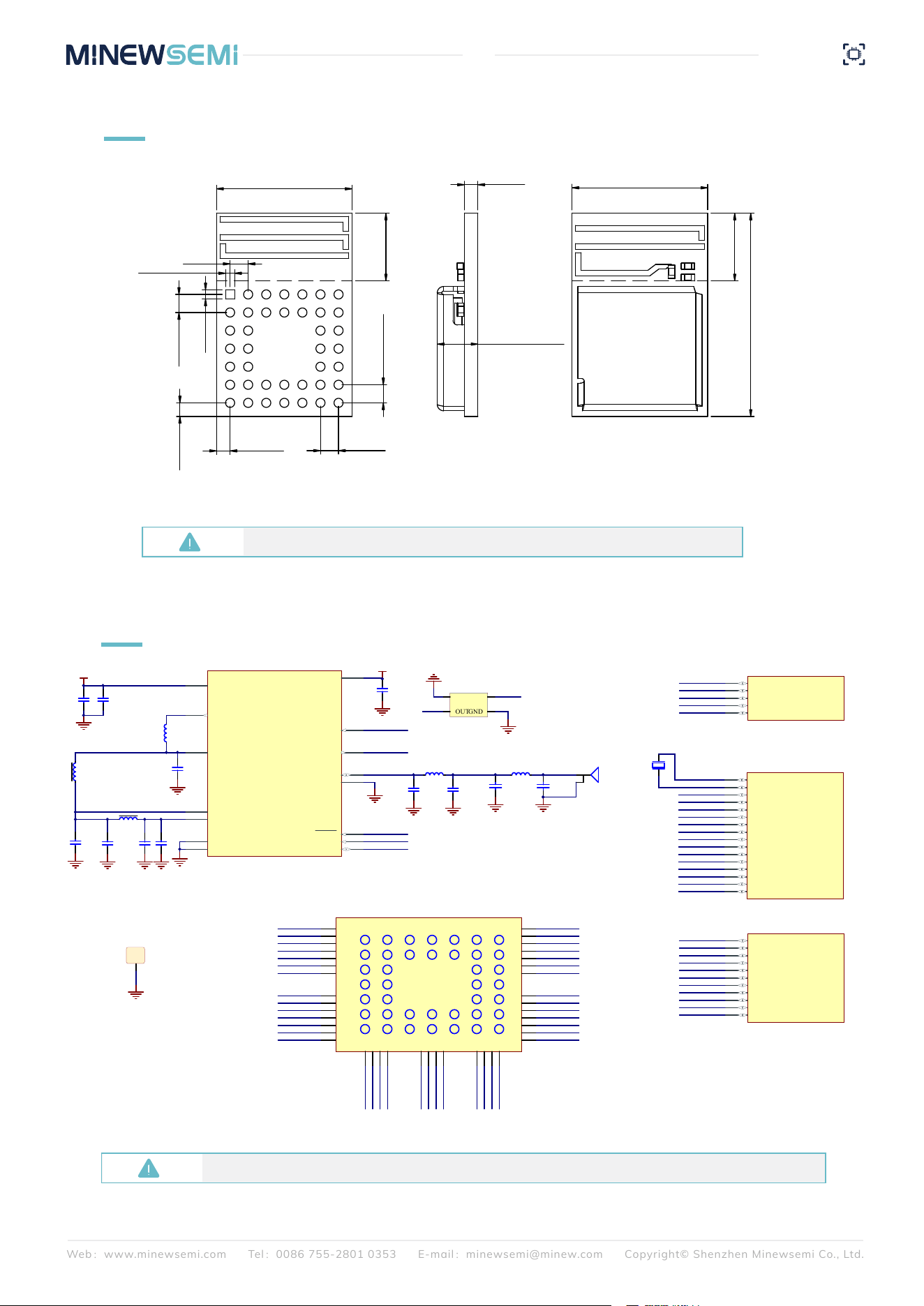
MECHANICAL DRAWING
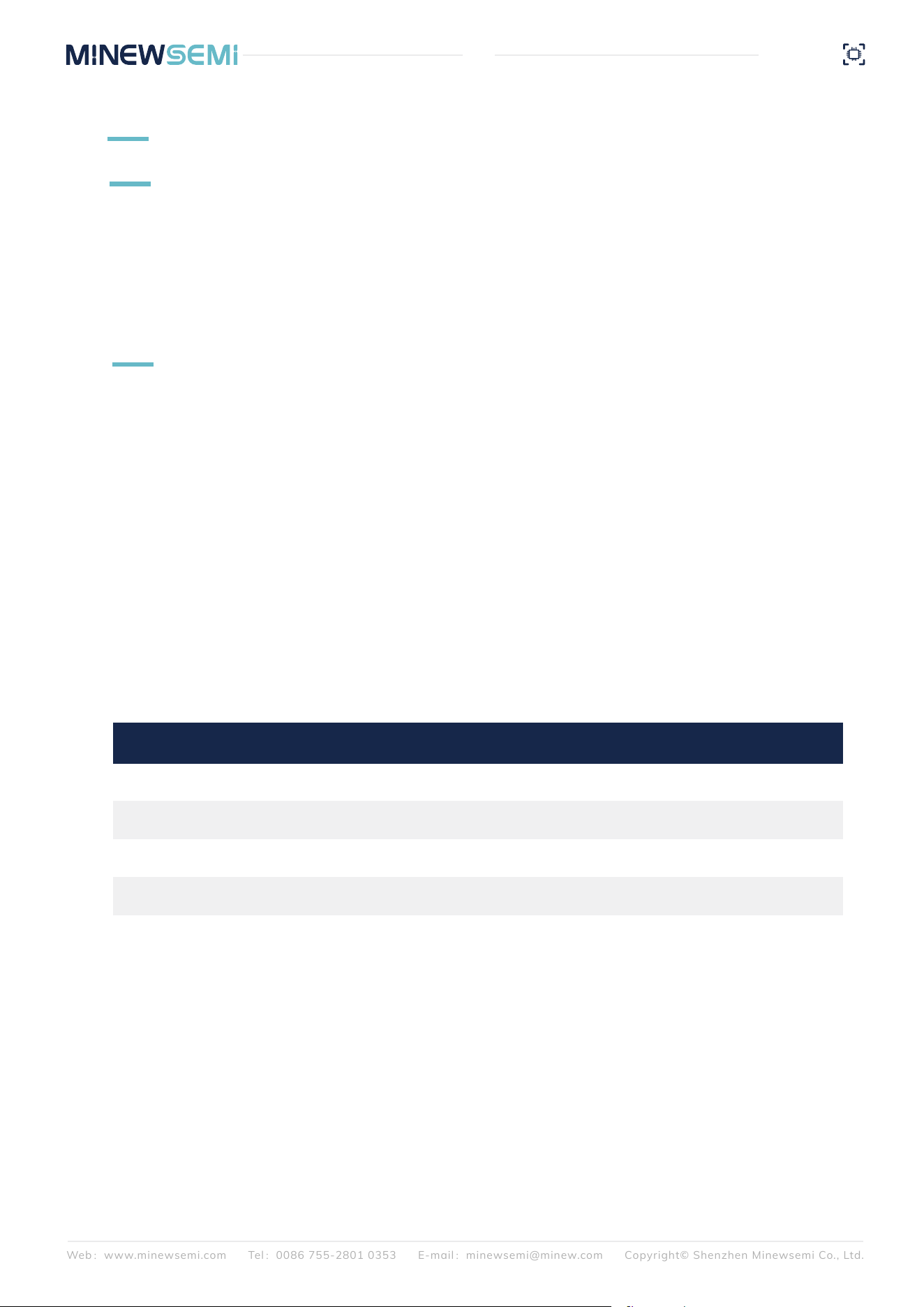
ELECTRICAL SCHEMATIC
Web:www.minewsemi.com Tel:0086 755-2801 0353 E-mail:minewsemi@minew.com Copyright© Shenzhen Minewsemi Co., Ltd.
07
ME54BS62
Datasheet
Default unit:mm Default tolerance:±0.15
Notice:Before placing an order, please confirm the specific configuration required with the salesperson.
DECA
A4
DECD
A5
VSS
A6
DCC
A7
VDD
B7
VSS
G4
DECRF
B1
ANT
D1
XC1
A1
XC2
A2
SWDIO
F2
VDD
G3
SWDCLK
E3
RESET
D2
VSS_PA
C2
nRF54L15
U1A
nRF54L15-CAAA
P0.02
E2
P0.03/CK
E1
P0.04/CK
D3
P0.00
G1
P0.01
F1
U1B
nRF54L15-CAAA
P1.00/XL1
C5
P1.08/EXTREF/CLK16M/CK
F7
P1.01/XL2
C6
P1.02/NFC1
C7
P1.03/NFC2/ CK
D5
P1.04/AIN0/CK
D6
P1.05/AIN1
E6
P1.06/AIN2
D7
P1.07/AIN3
E7
P1.10
C3
P1.11/AIN4/CK
C4
P1.12/AIN5/CK
A3
P1.13/AIN6
B4
P1.14/AIN7
B5
P1.09
B3
P1.15
B6
U1C
nRF54L15-CAAA
P2.00
G6
P2.01/CK
G7
P2.02
F6
P2.03
E5
P2.04
F5
P2.05
G5
P2.06/CK
F4
P2.07/SWO
E4
P2.08
D4
P2.09
F3
P2.10
G2
U1D
nRF54L15-CAAA
MC2
MC1
ML1
Y2
32.768kHz
GND
4
OUT
1
GND
2
IN
3
Y1
32MHz
GND
VCC
MC3
GND
DECD
GND
MC7
GND
VCC
GND
XC1
XC2
nRESET
SWDCLK
SWDIO
XC1
XC2
GND
GND
MC8 MC9
GND GND
P0.00
P0.01
P0.02
P0.03/CK
P0.04/CK
P1.00/XL1
P1.01/XL2
P1.02/NFC1
P1.03/NFC2/CK
P1.04/AIN0/CK
P1.05/AIN1
P1.06/AIN2
P1.07/AIN3
P1.08
P1.09
P1.10
P1.11/AIN4/CK
P1.12/AIN5/CK
P1.13/AIN6
P1.14/AIN7
P1.15
P2.00
P2.01/CK
P2.02
P2.03
P2.04
P2.05
P2.06/CK
P2.07/SWO
P2.08
P2.09
P2.10
A1
A2
A3
A4
A5
A6
A7
B1
B2
B3
B4
B5
B6
C1
C2
C6
C7
D1
D2
D6
D7
E1
E2
E6
E7
F1
F2
F3
F4
F5
F6
F7
A B C D E F
2
3
4
5
6
7
1
G
B7
G1
G2
G3
G4
G5
G6
G7
U2
ME54BS62
P0.03/CK
P0.04/CK
P2.09
GND
P2.07/SWO
P2.08
GND
P2.04
P2.01/CK
P2.00
P2.03
P2.05
P2.06/CK
P1.07/AIN3
P1.08
P2.02
SWDCLK
SWDIO
P0.00
nRESET
P1.06/AIN2
VCC
P0.01
GND
GND
P0.02
P2.10
P1.03/NFC2/CK
P1.02/NFC1
P1.09
P1.10
P1.13/AIN6
P1.12/AIN5/CK
P1.11/AIN4/CK
P1.14/AIN7
P1.15
P1.04/AIN0/CK
P1.05/AIN1
1
Shield
GND
ML2
GND
FB1
DECA
MC10
MC4
MC5
GND
GND
GND
MC6
GND
FB2
L1
C2
C1
1
2
Antenna1
ANT
GND GND
GND
0.6
0.6
0.8
0.8
0.4
0.4
0.8
0.8
3
6±0.15
0.6
1.8±0.15
6±0.15
9±0.15
3
Web:www.minewsemi.com Tel:0086 755-2801 0353 E-mail:minewsemi@minew.com Copyright© Shenzhen Minewsemi Co., Ltd.
08
ME54BS61
Datasheet
7
PCB DESIGN
This document is provided as a recommended design reference for wireless modules and does not constitute any
explicit or implied guarantee of performance or compliance. Due to differences in PCB layout, enclosure structure,
antenna selection, and application environments of the end product, this document cannot guarantee RF perfor-
mance in all scenarios. Users must conduct sufficient RF performance and compliance verification after completing
the final product design and shall bear full responsibility for design and application outcomes. Our company
reserves the right to modify the contents of this document without prior notice.
7.1 Disclaimer
Board Edge Priority Rule
The RF output/antenna side of the module must face the edge of the main PCB to ensure that antenna radiation is
directed outward from the board without obstruction. Placing the module in a closed central area of the PCB is
strictly prohibited.
Keep-Out Area Rule
A 0.5 mm area around the module body must be kept clear. Non-ground components and non-ground signal traces
are prohibited within this area. Within 4 mm around the RF side of the module, copper pours, unrelated compo-
nents, and non-RF signal traces are strictly prohibited.
Interference Isolation Rule
The module must maintain a minimum safe distance from strong interference sources. Adjacent placement on the
same layer is prohibited. Isolation using different PCB layers and shielding covers is recommended. General isola-
tion requirements are as follows:
7.2 Core Rules for Module Placement
20mm
20mm
15mm
25mm
Interference Source Type
Minimum Recommended Isolation Distance
Structural Clearance Rule
The minimum distance between the module and metal screws, clips, standoffs, and other structural parts must be
≥5 mm. At least 4 mm of SMT soldering and rework clearance must be reserved around the module. The RF side of
the module must not be enclosed inside a fully metal cavity.
Multiple Modules on the Same PCB
When placing multiple wireless modules of the same or different types on the same PCB, the minimum spacing
between modules must be ≥50 mm to avoid mutual interference.
DC-DC switching power supplies,
power inductors, power transformers
USB 3.0 / HDMI 2.0 / DDR
/ High-speed SDIO interfaces
MCU high-frequency clock circuits,
Ethernet PHY chips
Displays, cameras,
FPC cables with wiring
Web:www.minewsemi.com Tel:0086 755-2801 0353 E-mail:minewsemi@minew.com Copyright© Shenzhen Minewsemi Co., Ltd.
09
ME54BS61
Datasheet
Grounding Design
The main PCB must maintain a complete and continuous ground plane. Splitting the ground plane within the
module projection area or RF surrounding area is strictly prohibited. All module ground pins must be soldered. At
least one grounding via should be placed near each ground pad and connected to the main ground plane. A
complete ground plane with dense grounding vias may be placed under the non-RF area of the module to improve
shielding performance.
Power Supply Design
Decoupling capacitor combinations must be placed close to the module power input pins. The trace length between
capacitor pads and power pins should be ≤0.5 mm, and at least two grounding vias should be placed near the
ground terminal. For switching power supply applications, a π-type filter circuit footprint must be reserved near the
module power input pins.
RF Trace Design
The entire RF path must maintain a strict 50 Ω characteristic impedance (tolerance ±10%). RF traces should be as
short as possible and routed preferably in straight lines. Sharp or right-angle corners are prohibited; curved routing
with a radius ≥3 times the trace width is recommended. Branch traces and stub traces are prohibited. A continuous
reference ground plane must exist beneath the RF traces, and no other signal traces should be routed within 3
times the trace width on either side. Ground shielding should be applied throughout the RF routing.
Control Interface Design
Control signal traces such as UART, SPI, and I2C should be routed away from RF areas with short and simple
routing paths and continuous ground shielding. Parallel routing adjacent to RF traces is prohibited. ESD protection
devices must be placed close to external PCB connectors and must not be placed near module pins.
Footprint Design
Strictly use the standard PCB footprint provided by our company. Unauthorized modification of pad size or spacing
is prohibited to ensure soldering reliability.
7.3 GENERAL PCB DESIGN REQUIREMENTS
Do not place the RF side of the module facing the inside of the PCB or away from the board edge.
Do not place copper pours, components, or fully enclosed metal housings without openings over the antenna
area.
Do not route RF traces across split ground planes, without a complete reference ground, or with right-angle
corners.
Do not place modules adjacent to strong interference sources or split the ground plane in the module area.
Do not leave module ground pins unconnected or inadequately grounded.
7.4 DESIGN RESTRICTIONS
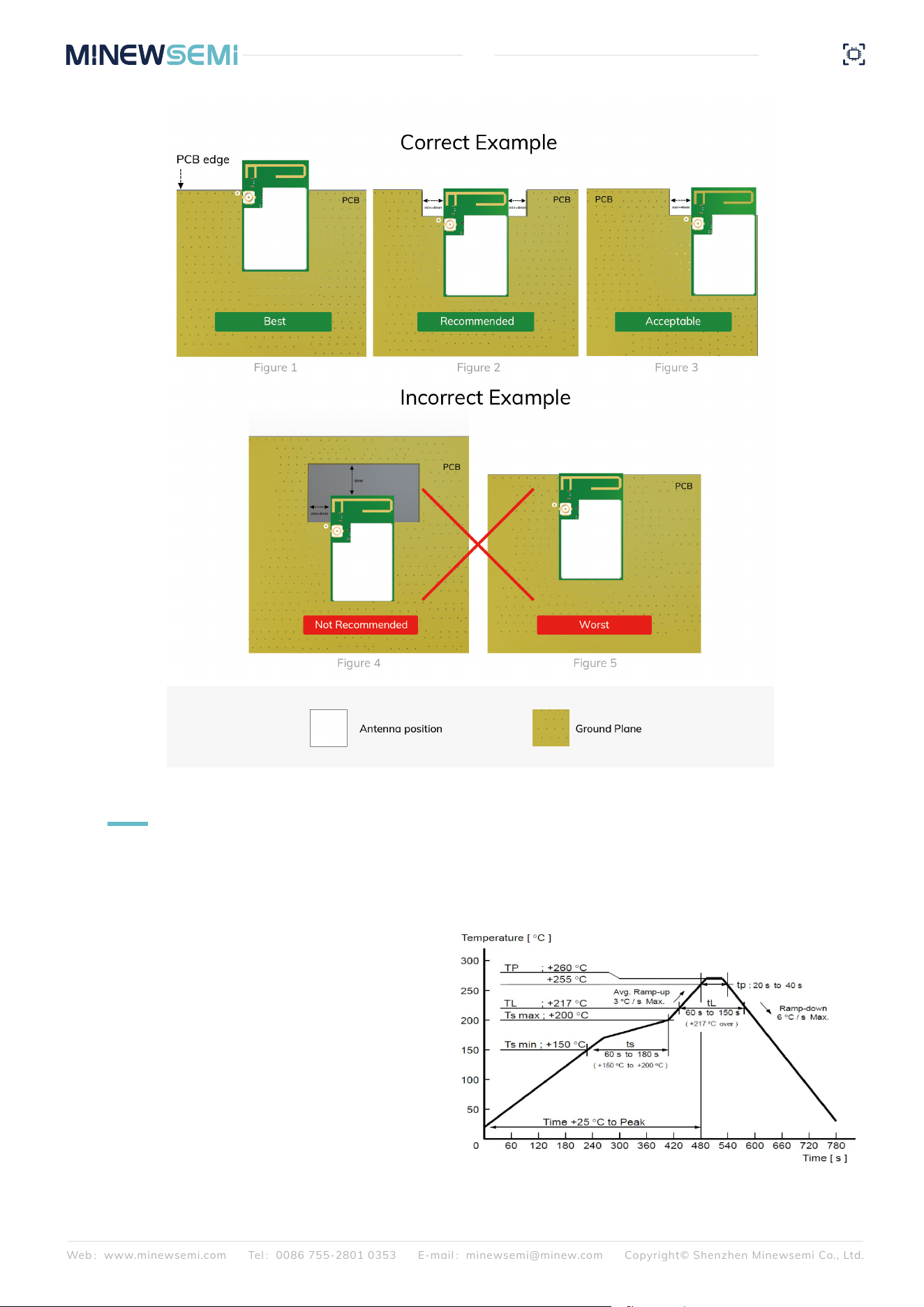
For end products, antenna position significantly affects overall system performance. The module should preferably
be placed at the edge or corner of the PCB to maximize the clearance area and reduce interference from surround-
ing components. The PCB area directly beneath the module antenna should be hollowed out to keep the antenna
region suspended, while no signal traces, metal objects, or other interference sources should exist within 3–5 mm
around the antenna area. The figure below demonstrates an example of proper module placement on the main
PCB for optimal RF performance. The first recommended layout method should be used whenever possible, as the
module antenna design has been tuned and optimized based on this configuration.
7.5 MODULE PLACEMENT EXAMPLE
8
REFLOW AND SOLDERING
Web:www.minewsemi.com Tel:0086 755-2801 0353 E-mail:minewsemi@minew.com Copyright© Shenzhen Minewsemi Co., Ltd.
10
ME54BS61
Datasheet
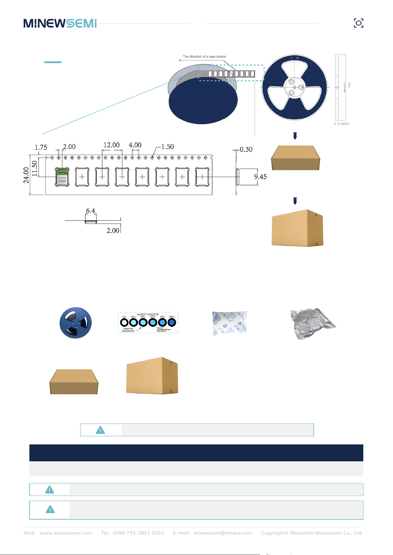
1) Perform SMT according to the reflow oven temperature profile provided below, with a maximum temperature of 260°C;
2) Follow IPC/JEDEC standards; Peak temperature: < 260°C; Number of reflows: ≤2 times; For SMT involving double-sided
placement, it is recommended that the module side undergoes reflow soldering only once. For any special processes, please
contact our company.
3)Module SMT recommended stencil thickness
0.1-0.12mm, pin 1:0.9 opening, not expanded;
4)After opening, if the entire package is not used at
once, it should be stored in a vacuum to prevent
long-term exposure to air, which can cause moisture
absorption and pad oxidation. If there is a gap of 7 to 30
days before reuse, it is recommended to bake the tape at
65-70°C for 24 hours without unrolling it before returning
to SMT.
5) ESD protection measures should be implemented
before using SMT.
9
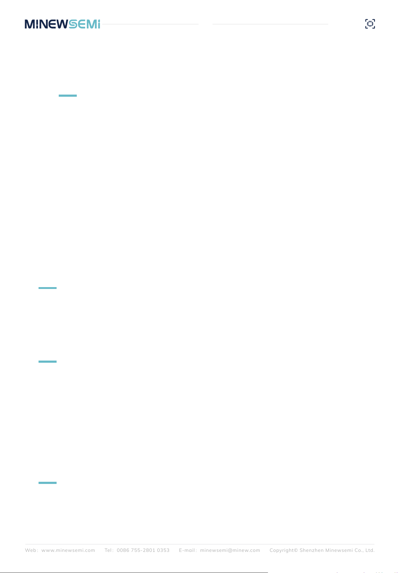
ME54BS62 1900PCS 319.2g 1709.2g
W=24mm,T=0.30mm
Packing detail Specification Net weight Gross weight Dimension
PACKAGE INFORMATION
Carrier tape packaging tray Humidity Indicator
(1 pcs/bag)
Desiccant
(placed in a vacuum bag)
Vacuum bag
Moisture-proof label (attached to the vacuum bag)
Certification label (attached to the vacuum bag)
Outer box label
Inner carton(*8)
355*345*35mm,±5mm
Inner carton(*8)
355*345*35mm,±5mm
370*358*350mm,±10mm
Outer carton
370*358*350mm,±10mm
Outer carton
Note: Default weight tolerance all are within 10g(except the special notes)
Net Weight: Weight of a single roll of the module product, excluding packaging materials;
Gross Weight: Weight of a single roll of the product, including the carrier tape, industrial inner box, and outer carton.
Default unit:mm Default tolerance:±0.1
Remarks
General material list for FCL packaging:
Other:
Web:www.minewsemi.com Tel:0086 755-2801 0353 E-mail:minewsemi@minew.com Copyright© Shenzhen Minewsemi Co., Ltd.
11
ME54BS61
Datasheet
Web:www.minewsemi.com Tel:0086 755-2801 0353 E-mail:minewsemi@minew.com Copyright© Shenzhen Minewsemi Co., Ltd.
12
ME54BS12
Datasheet
This device complies with part 15 of the FCC Rules. Operation is subject to the following two conditions:
(1) This device may not cause harmful interference
(2) This device must accept any interference received, including interference that may cause undesired operation.
Any Changes or modifications not expressly approved by the party responsible for compliance could void the user's
authority to operate the device.
Note: This device has been tested and found to comply with the limits for a Class B digital device, pursuant to part 15
of the FCC Rules. These limits are designed to provide reasonable protection against harmful interference in a residen-
tial installation. This device generates uses and can radiate radio frequency energy and, if not installed and used in
accordance with the instructions, may cause harmful interference to radio communications. However, there is no guar-
antee that interference will not occur in a particular installation. If this device does cause harmful interference to radio
or television reception, which can be determined by turning the device off and on, the user is encouraged to try to correct
the interference by one or more of the following measures:
-Reorient or relocate the receiving antenna.
-Increase the separation between the device and receiver.
-Connect the device into an outlet on a circuit different from that to which the receiver is connected.
-Consult the dealer or an experienced radio/TV technician for help.
This module complies with FCC RF radiation exposure limits set forth for an Uncontrolled environment, This equipment
should be installed and operated with a minimum distance of 20 centimeters between the radiator and your body.
10
FCC WARNING
Requirement per KDB996369 D03
List the FCC rules that are applicable to the modular transmitter. These are the rules that specifically establish the
bands of operation, the power, spurious emissions, and operating fundamental frequencies. DO NOT list compli-
ance to unintentional-radiator rules (Part 15 Subpart B) since that is not a condition of a module grant that is
extended to a host manufacturer. See also Section 2.10 below concerning the need to notify host manufacturers
that further testing is required.3Explanation: This module meets the requirements of FCC part 15C(15.247).
2.2 List of applicable FCC rules
Describe use conditions that are applicable to the modular transmitter, including for example any limits on anten-
nas, etc. For example, if point-to-point antennas are used that require reduction in power or compensation for cable
loss, then this information must be in the instructions. If the use condition limitations extend to professional users,
then instructions must state that this information also extends to the host manufacturer’s instruction manual. In
addition, certain information may also be needed, such as peak gain per frequency band and minimum gain, specif-
ically for master devices in 5 GHz DFS bands.
Explanation: The EUT has a PCB Antenna, , and the antenna use a permanently attached
Antenna which is not replaceable.
2.3 Summarize the specific operational use conditions
If a modular transmitter is approved as a “limited module”, then the module manufacturer is responsible for approv-
ing the host environment that the limited module is used with. The manufacturer of a limited module must describe,
both in the filing and in the installation instructions, the alternative means that the limited module manufacturer
uses to verify that the host meets the necessary requirements to satisfy the module limiting conditions.
2.4 Limited module procedures

Web:www.minewsemi.com Tel:0086 755-2801 0353 E-mail:minewsemi@minew.com Copyright© Shenzhen Minewsemi Co., Ltd.
13
ME54BS12
Datasheet
A limited module manufacturer has the flexibility to define its alternative method to address the conditions that limit
the initial approval, such as: shielding, minimum signaling amplitude, buffered modulation/data inputs, or power
supply regulation. The alternative method could include that the limited module manufacturer reviews detailed test
data or host designs prior to giving the host manufacturer approval.
This limited module procedure is also applicable for RF exposure evaluation when it is necessary to demonstrate
compliance in a specific host. The module manufacturer must state how control of the product into which the
modular transmitter will be installed will be maintained such that full compliance of the product is always ensured.
For additional hosts other than the specific host originally granted with a limited module,a Class II permissive
change is required on the module grant to register the additional host as a specific host also approved with the
module.
Explanation: The module is not a limited module.
For a modular transmitter with trace antenna designs, see the guidance in Question 11 of KDB Publication 996369
D02 FAQ – Modules for Micro-Strip Antennas and traces. The integration information shall include for the TCB
review the integration instructions for the following aspects: layout of trace design, parts list (BOM), antenna,
connectors, and isolation requirements.
a) Information that includes permitted variances (e.g., trace boundary limits, thickness, length, width, shape(s),
dielectric constant, and impedance as applicable for each type of antenna);
b) Each design shall be considered a different type (e.g., antenna length in multiple(s) of frequency, the wave-
length, and antenna shape (traces in phase) can affect antenna gain and must be considered);
c) The parameters shall be provided in a manner permitting host manufacturers to design the printed circuit (PC)
board layout;
d) Appropriate parts by manufacturer and specifications;
e) Test procedures for design verification;
f) Production test procedures for ensuring compliance.
The module grantee shall provide a notice that any deviation(s) from the defined parameters of the antenna trace,
as described by the instructions, require that the host product manufacturer must notify the module grantee that
they wish to change the antenna trace design. In this case, a Class II permissive change application is required to
be filed by the grantee, or the host manufacturer can take responsibility through the change in FCC ID (new applica-
tion) procedure followed by a Class II permissive change application.
Explanation: Yes, The module with trace antenna designs, and This manual has been shown the layout of trace
design,, antenna, connectors, and isolation requirements.
2.5 Trace antenna designs
It is essential for module grantees to clearly and explicitly state the RF exposure conditions that permit a host prod-
uct manufacturer to use the module. Two types of instructions are required for RF exposure information:
(1) to the host product manufacturer, to define the application conditions (mobile, portable – 20 cm from a person’s
body); and (2) additional text needed for the host product manufacturer to provide to end users in their end-product
manuals. If RF exposure statements and use conditions are not provided, then the host product manufacturer is
required to take responsibility for the module through a change in FCC ID (new application).
Explanation: This module complies with FCC RF radiation exposure limits set forth for an Uncontrolled environment,
This equipment should be installed and operated with a minimum distance of 20 centimeters between the radiator
and your body. This module is designed to comply with the FCC statement, FCC ID is: 2BDJ6-ME54BS62
2.6 RF exposure considerations
Web:www.minewsemi.com Tel:0086 755-2801 0353 E-mail:minewsemi@minew.com Copyright© Shenzhen Minewsemi Co., Ltd.
14
ME54BS12
Datasheet
Grantees are responsible for the continued compliance of their modules to the FCC rules. This includes advising host
product manufacturers that they need to provide a physical or e-label stating “Contains FCC ID” with their finished
product. See Guidelines for Labeling and User Information for RF Devices – KDB Publication 784748.
Explanation:The host system using this module, should have label in a visible area indicated the following texts:
"Contains FCC ID: 2BDJ6-ME54BS62
2.8 Label and compliance information
A list of antennas included in the application for certification must be provided in the instructions.
For modular transmitters approved as limited modules, all applicable professional installer instructions must be
included as part of the information to the host product manufacturer. The antenna list shall also identify the anten-
na types (monopole, PIFA, dipole, etc. (note that, for example, an “omnidirectional antenna” is not considered to be
a specific “antenna type”).
For situations where the host product manufacturer is responsible for an external connector, for example, with an
RF pin and antenna trace design, the integration instructions shall inform the installer that a unique antenna
connector must be used on the Part 15 authorized transmitters used in the host product. The module manufactur-
ers shall provide a list of acceptable unique connectors.
Explanation: The EUT has a PCB Antenna, and the antenna uses a permanently attached antenna, which is unique.
2.7 Antennas
Additional guidance for testing host products is given in KDB Publication 996369 D04 Module Integration Guide.
Test modes should take into consideration different operational conditions for a stand-alone modular transmitter
in a host, as well as for multiple simultaneously transmitting modules or other transmitters in a host product.
The grantee should provide information on how to configure test modes for host product evaluation for different
operational conditions for a stand-alone modular transmitter in a host, versus with multiple, simultaneously trans-
mitting modules or other transmitters in a host.
Grantees can increase the utility of their modular transmitters by providing special means, modes, or instructions
that simulates or characterizes a connection by enabling a transmitter. This can greatly simplify a host manufactur-
er’s determination that a module as installed in a host complies with FCC requirements.
Explanation: Topband can increase the utility of our modular transmitters by providing instructions that simulates
or characterizes a connection by enabling a transmitter.
2.9 Information on test modes and additional testing requirements
Please use this product within 6 months after signing the receipt.
- This product should be stored without opening the package at an ambient temperature of 5~35°C and
a humidity of 20~70%RH.
- This product should be left for more than 6 months after receipt and should be confirmed before use.
- The product must be stored in a non-corrosive gas (CI2, NH3, SO2, NOx, etc.).
- To avoid damaging the packaging material, do not apply any excessive mechanical shocks, including but
not limited to sharp objects adhering to the packaging material and product dropping.
This product is suitable for MSL2 (based on JEDEC standard J-STD-020).
- After opening the package, the product must be stored at ≤30°C/<60%RH. It is recommended to use the
product within 3-6 months after opening the package.
- When the color of the indicator in the package changes, the product should be baked before welding.
Baking is not required for one year if exposure is limited to <30°C and 60%RH. Refer to MSL2 for exposure
criteria for moisture sensitivity level. If exposed to (≥168h@85°C/60%RH) conditions or stored for more than
one year, recommended baking conditions.
1. 120 +5/-5°C, 8 hours, 1 time
Products must be baked individually on heat-resistant trays because the materials (base tape, reel tape, and
cover tape) are not heat-resistant, and the packaging material may be deformed at temperatures of 120℃;
2、90℃ +8/-0℃,24hours,1times
The base tape can be baked together with the product at this temperature. Please pay attention to the unifor-
mity of heat.
• Be careful in handling or transporting products because excessive stress or mechanical shock may break
products.
• Handle with care if products may have cracks or damages on their terminals. If there is any such damage, the
characteristics of products may change. Do not touch products with bare hands that may result in poor solder
ability and destroy by static electrical charge.
Cognizant of our commitment to quality, we operate our own factory equipped with state-of-the-art production facilities and
a meticulous quality management system. We hold certifications for ISO9001, ISO14001, ISO27001, OHSA18001, BSCI.
Every product undergoes stringent testing, including transmit power, sensitivity, power consumption, stability, and aging
tests. Our fully automated module production line is now in full operation, boasting a production capacity in the millions, capa-
ble of meeting high-volume production demands.
13
QUALITY
11
STORAGE CONDITIONS
12
HANDLING CONDITIONS
Web:www.minewsemi.com Tel:0086 755-2801 0353 E-mail:minewsemi@minew.com Copyright© Shenzhen Minewsemi Co., Ltd.
15
ME54BS61
Datasheet
This manual and all the contents contained in it are owned by Shenzhen Minewsemi Co., Ltd. and are protected by Chinese
laws and applicable international conventions related to copyright laws.
The certified trademarks included in this product and related documents have been licensed for use by MinewSemi. This
includes but is not limited to certifications such as BQB, RoHS, REACH, CE, FCC, BQB, IC, SRRC, TELEC, WPC, RCM, WEEE,
etc. The respective textual trademarks and logos belong to their respective owners. For example, the Bluetooth® textual
trademark and logo are owned by Bluetooth SIG, Inc. Other trademarks and trade names are those of their respective owners.
Due to the small size of the module product, the "®" symbol is omitted from the Bluetooth Primary Trademarks information in
compliance with regulations.
The company has the right to change the content of this manual according to the technological development, and the revised
version will not be notified otherwise. Without the written permission and authorization of the company, any individual,
company, or organization shall not modify the contents of this manual or use part or all of the contents of this manual in other
ways. Violators will be held accountable in accordance with the law.
14
COPYRIGHT STATEMENT
15
RELATED DOCUMENTS
16
ME54BS61
Datasheet
For product change notifications and regular updates of Minewsemi documentation,
please register on our website: www.minewsemi.com
MinewSemi_Product_Naming_Reference_Manual
https://en.minewsemi.com/file/MinewSemi_Product_Naming_Reference_Manual_EN.pdf
MinewSemi_Connectivity_Module_Catalogue
https://en.minewsemi.com/file/MinewSemi_Connectivity_Module_Catalogue_EN.pdf
https://store.minewsemi.com
https://minewsemi.com
Gangzhilong Technology Park, Qinglong Road, Longhua
District, Shenzhen
minewsemi@minew.com
0086-755-2801 0353
SHENZHEN MINEWSEMI CO., LTD.
Innovative IoT Module Expert

