Loading ...
Loading ...
Loading ...
-15-
In practice, the current through the diodes is not as shown in Figure 2C. Because
c
apacitor C5 has a charge after the first cycle, the diode will not conduct until the
p
ositive AC voltage exceeds the positive charge in the capacitor. Figure 5 shows
a better picture of what the current flow looks like, assuming no loss in the diode.
It takes a few cycles for the voltage to build up on the capacitor. This depends on
the resistance of the winding and diode. After the initial start-up, there will be a
charge and discharge on the capacitor depending on the current drawn by the
output load. Remember current only flows through the diode when the anode is
more positive than the cathode. Thus, current will flow in short bursts as shown in
Figure 5C.
The DC load current may be one ampere, but the peak diode current may be three times that. Therefore, the
diode rating must be sufficient to handle the peak current. The 1N4001 has peak current rating of 10 amps.
Regulator Circuit
The regulator circuit in the Model XP-720 power supply consists of a LM-317
integrated circuit. This IC is specially designed to perform the regulation
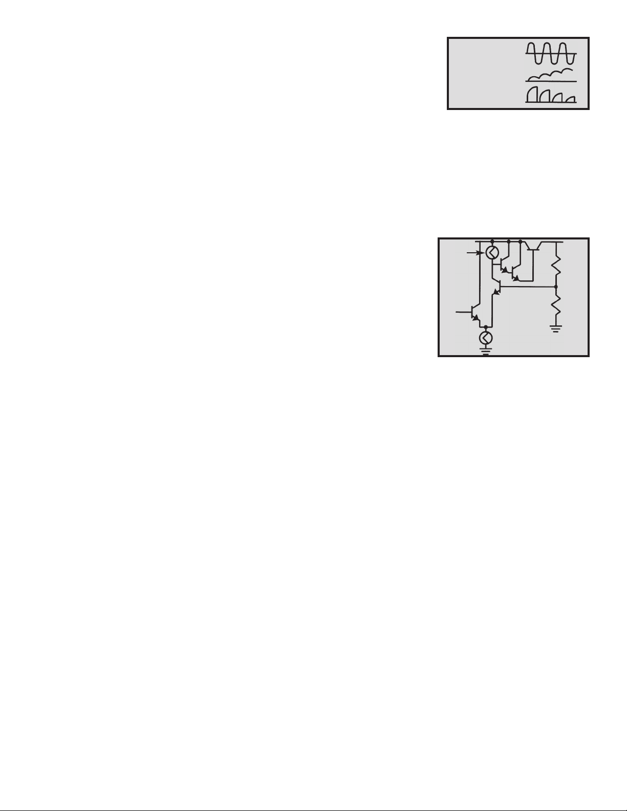
function. Figure 6 shows a simplified circuit of how the LM-317 IC works.
Transistors Q1 and Q2 form a circuit known as a differential amplifier.
Transistor Q1 base is connected to a stable 1.5V reference voltage. The base
of Q2 is connected to the regulator output circuit through a voltage divider
network. The collector of transistor Q2 is connected to a current source. This
basically is a PNP transistor biased to draw about 1mA of current. Transistor
Q2 sees the current source as a very high resistor of about 1 meg ohms. Thus,
the gain of transistor Q2 is extremely high.
Transistor Q5 is called the pass transistor. It controls the current reaching the output. Transistors Q3 and Q4
are emitter followers. Their function is to raise the impedance of the pass transistor. Note that transistors Q2,
Q3, Q4 and Q5 and resistor R1 form a close loop. Also, note that the feedback to the base of Q2 is negative,
that is, when the base of Q2 goes positive, the output at emitter Q5 goes negative. Now if the 1.25V output
voltage goes down because of current drain at the output, the base of Q2 will drop forcing the collector voltage
of Q2 to go higher. This will bring the output voltage back to 1.25V. This is the basis of all negative regulators.
Another feature of the LM-317 regulator is to protect the IC against overload and output shorts. If the IC is
overloaded, the junction of an overload transistor will overheat. A transistor will sense this overheating and shut
down transistor Q5.
Figure 5
A) Transformer
Winding
B) Voltage C1
C) Current
through diodes
20V
Peak
20V
Figure 6
1.25V
Output
R1
R2
Divider
Q1
Q2
1.5V
Q
3
Q
4
Q
5
Current
Source
Equalized
t
o 1 Meg.
XP-720K_REV-H_111114.qxp_XP-720K REV-H 111114 7/31/15 1:08 PM Page 16
Loading ...
Loading ...
Loading ...