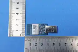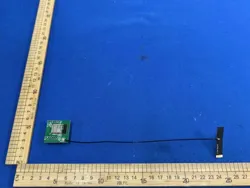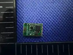

i
MN54LM Bluetooth® Low Energy Module
操作手冊
BLE Solution: Nordic NRF54LM20A
RF IC
Crystal
Chip antenna
Nordic NRF54LM20A/V1
32MHz/20ppm
Embedded
Embedded

Overview and Benefits
Overview(概述)
The MN54LM from Aradconn is a highly flexible, ultra-low power, Bluetooth Low Energy
module based on the nRF54LM20A SoC from Nordic Semiconductor. With an Arm® Cortex®-M33
with FPU 32-bit processor, embedded 2.4GHz transceiver, and integrated chip antenna. Providing
full use of the nRF54LM20A’s capabilities and peripherals, which include I2C, SPI, UART, I2S, ADC,
GPIO, PWM interfaces.
愛瑞德 MN54LM-C 產品為基於 Nordic Semiconductor 的 nRF54LMA20 SoC 晶片所開發高適用
性且低能耗的藍芽模組。 FPU 32 位元處理器、嵌入式 2.4GHz 收發器和整合式晶片天線的
Arm® Cortex®-M33。充分利用 nRF54LM20A 的功能和周邊,包括 I2C、SPI、UART、I2S、
ADC、GPIO、PWM 介面。
Benefits(優點)
• Bluetooth qualification and Regulatory certification reduce the
burden to enter the market.
具備藍牙資格和監管認證減輕了進入市場的負擔。
• Complete RF solution with no additional RF design, allowing faster
time to launch a new product, and providing long working distance.
具備完整的無線射頻解決方案,無需額外的射頻設計,可以更快地推出新產品,並提
供遠距離工作範圍。
MN54LM: up to 500 meters in open space. @1 Mbps
於開放場域 1Mbps 具 500 公尺的傳輸距離。
• Compact size: (L) 13 x (W) 7.5 x (H) 2.0mm.
產品尺寸(L) 13 x (W) 7.5 x (H) 2.0mm。
• Provides flexibility in the OEM’s application development choice
with full support for using Nordic SDK and firmware tools.
針對 OEM 開發應用提供完整的 Nordic SDK 及韌體工具支援。

1
1. Features (功能)
• 2.4 GHz transceiver
• -95.5 dBm sensitivity in 1Mbps Bluetooth® low energy mode
• -103 dBm sensitivity in 125kbps Bluetooth® low energy mode(long range)
• -10 to +8dBm TX power, configurable in 1 dB steps
• Supported data rates:
• Bluetooth® LE –LE 2 M, LE 1 Mbps, LE Coded
• 10.9 mA/ @3V DC/DC peak current in TX (8 dBm)
• 3.3 mA/@3V DC/DC peak current in RX
• RSSI (1 dB resolution)
• Arm® Cortex®-M33 32-bit processor with TrustZone® technology, 128 MHz
• 503 CoreMark®,3.93 CoreMark/MHz EEMBC CoreMark executing from non-volatile memory
• Single-precision floating-point unit (FPU)
• Memory protection unit (MPU)
• Digital signal processing (DSP) instructions
• Serial wire debug (SWD)
• Memory
• 2.036MB NVM/512 kB RAM
• Coprocessor
• RISC-V 128MHZ Coprocessor
• Operating condition
• 1.7 V to 3.6 V supply and I/O voltage
• Single 32 MHz crystal operation
• Optional 32.768 kHz clock
• Operating temperature from -40°C to 85°C

• Peripherals
• 30 general purpose I/O pins
• High-Speed USB interface(USBHS)
• Global RTC (GRTC) that can run in System OFF mode and implement a shared system timer
• Seven 32-bit timers with counter mode
• Two individual watchdog timers for secure and non-secure context (WDT)
• Up to seven fully featured serial interfaces with EasyDMA ,supporting I2C, SPI and UART
• One high-speed SPIM up to 32 MHz, six up to 8 MHz
• One high-speed UARTE up to 4 Mbps, six up to 1 Mbps
• Six TWI up to 400 kHz and I2C compatible
• I2S two channel Inter-IC sound interface
• Pulse density modulation (PDM) interface
• Three pulse width modulation (PWM) four-channel units with autonomous waveform generator.
• SAADC with up to eight programmable gain channels.
14-bit at 62.5ksps, 12-bit at 125 ksps, and up to 10-bit at 2 Msps.
• Two quadrature decoders (QDEC)
• Comparator and low-power comparator with wake-up from System OFF mode
• Temperature sensor
3
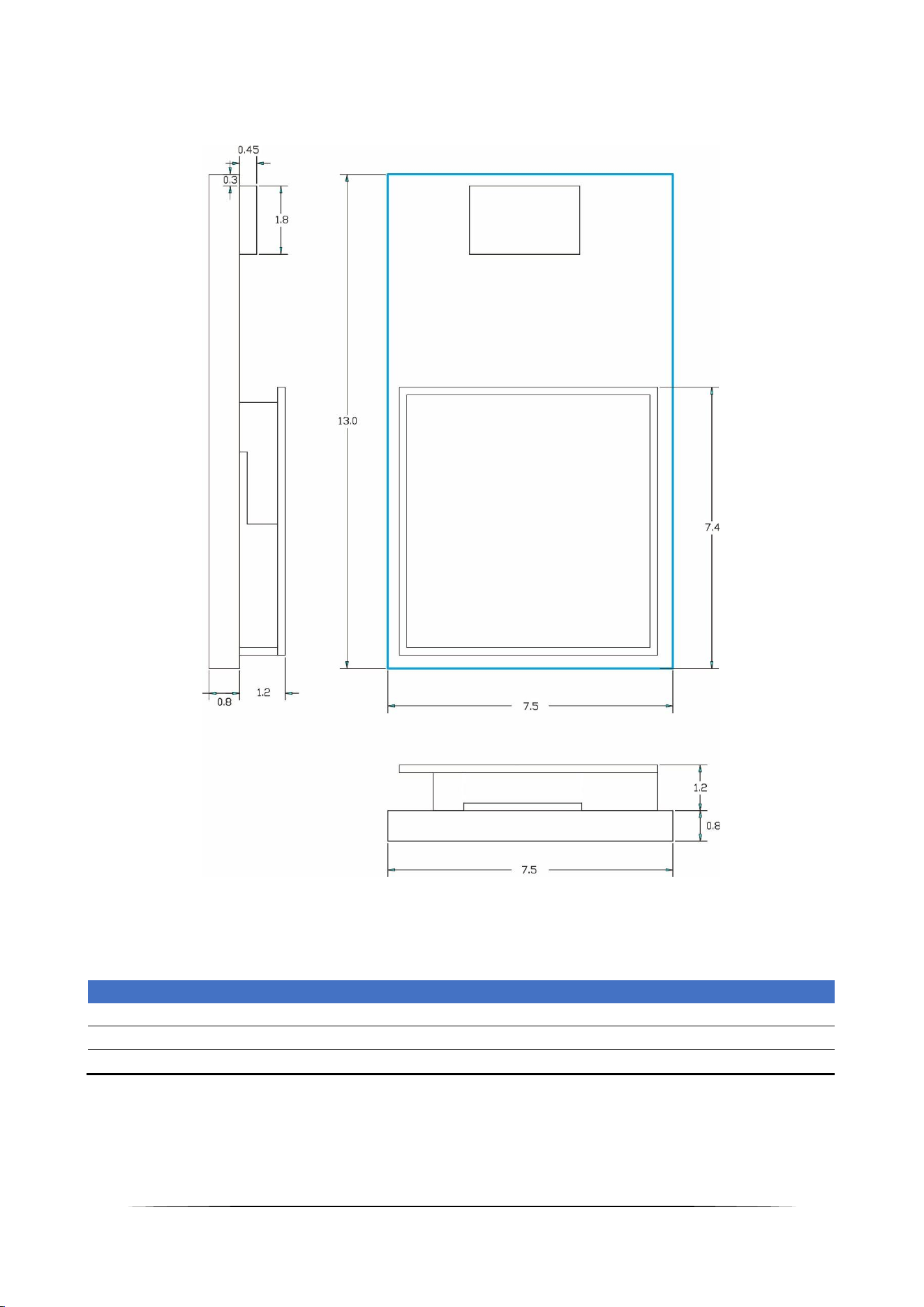
2.1 Dimensions
All dimensions are in millimeters.
Item
Dimension
Tolerance
Length
13.0mm
±0.30 mm
Width
7.5mm
±0.30mm
Height
2.0mm
±0.30mm
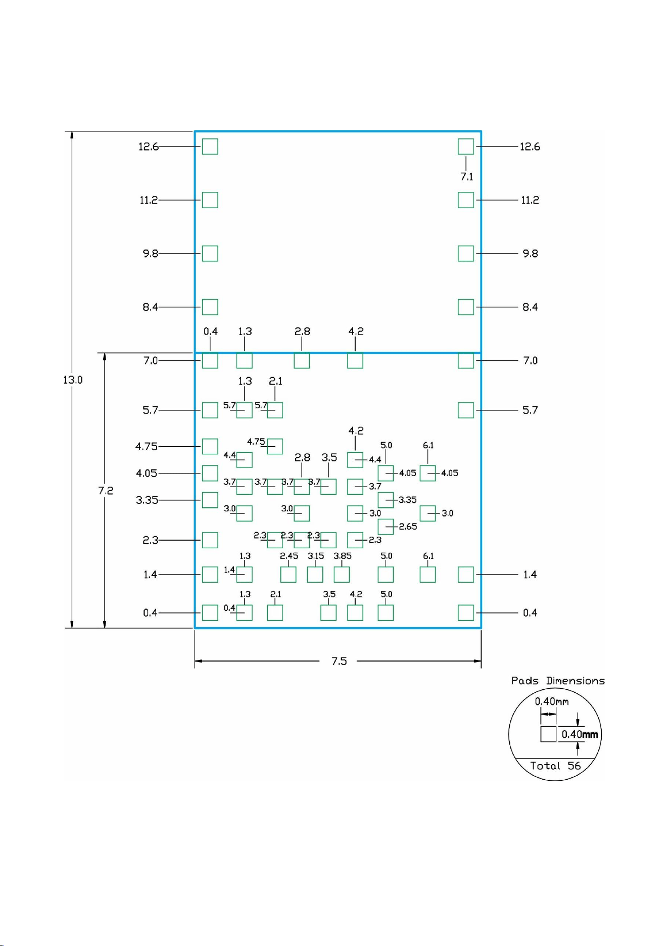
2.2 Footprint
All dimensions are in millimeters.
5
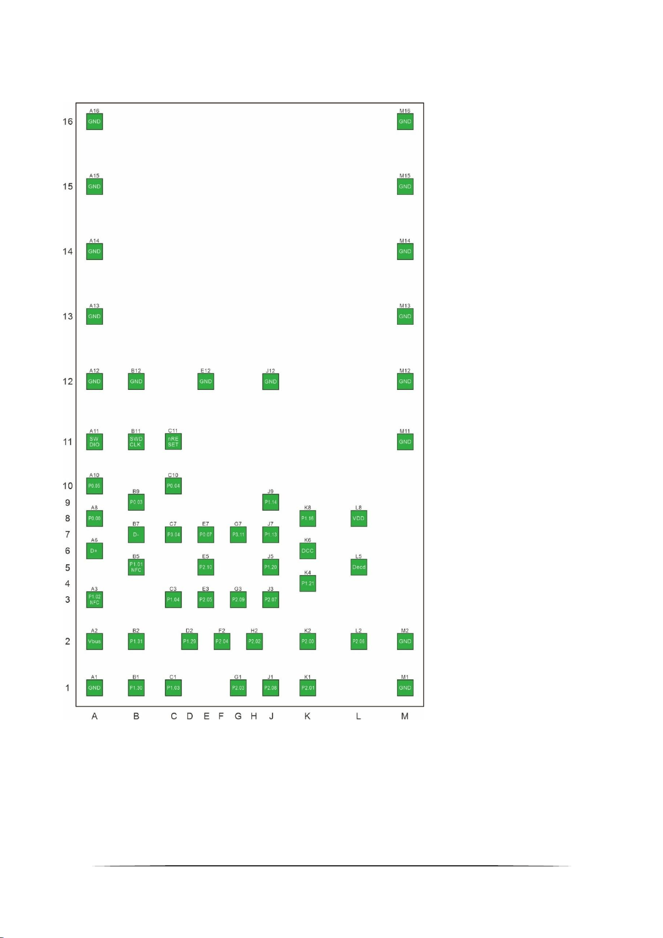
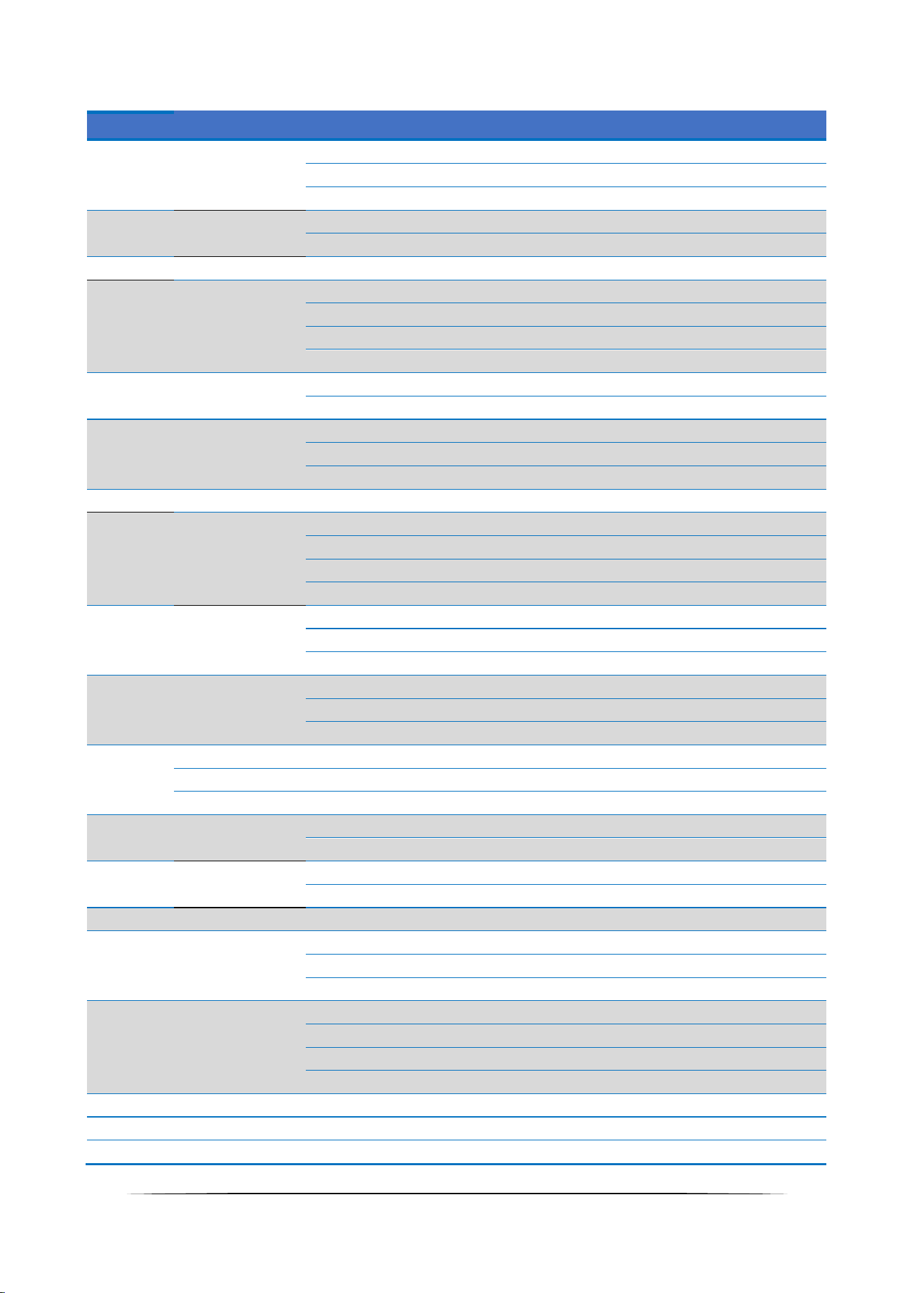
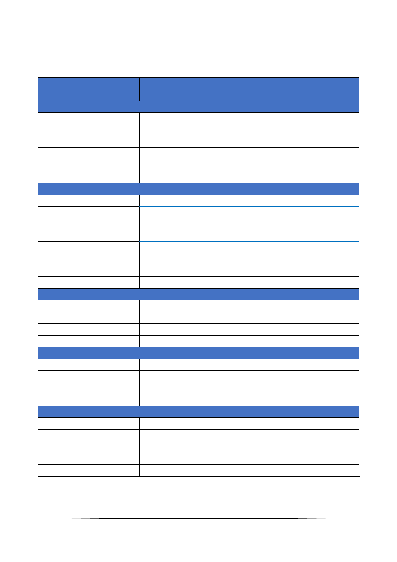
3. Pin Assignment

Pin No.
Name
Pin function
Description
(A1)
GND
Ground
The pad must be connected to a solid ground plane
(A2)
VBUS
Power
USB 5V supply
(A3)
P1.02
Digital I/O
General-purpose I/O
NFC2
NFC input
NFC antenna connection
(A6)
D+
Analog I/O
USB D+ line
(A8)
P0.00
Digital I/O
General-purpose I/O
(A10)
P0.05
Digital I/O
General-purpose I/O
(A11)
SWDIO
Debug
Serial wire data. Bidirectional with standard-drive
and on-chip pull-up.
(A12)
GND
Ground
The pad must be connected to a solid ground plane
(A13)
GND
Ground
The pad must be connected to a solid ground plane
(A14)
GND
Ground
The pad must be connected to a solid ground plane
(A15)
GND
Ground
The pad must be connected to a solid ground plane
(A16)
GND
Ground
The pad must be connected to a solid ground plane
(B1)
P1.30
Digital I/O
General-purpose I/O
AIN2
Analog input
Analog input
(B2)
P1.31
Digital I/O
General-purpose I/O
AIN1
Analog input
Analog input
(B5)
P1.01
Digital I/O
General-purpose I/O
NFC1
NFC input
NFC antenna connection
(B7)
D-
Analog I/O
USB D- line
(B9)
P0.03
Digital I/O
General-purpose I/O
GRTC PWM
Clock PIN
GRTC PWM output
(B11)
SWDCLK
Debug
Serial wire clock. Input with on-chip pull-down.
(B12)
GND
Ground
The pad must be connected to a solid ground plane
(C1)
P1.03
Digital I/O
General-purpose I/O
AIN7
Analog input
Analog input
Clock pin
Can be set as TWI
(C3)
P1.04
Digital I/O
General-purpose I/O
AIN6
Analog input
Analog input
Clock pin
Can be set as TWI
(C7)
P3.04
Digital I/O
General-purpose I/O
Clock pin
Can be set as TWI
(C10)
P0.04
Digital I/O
General-purpose I/O
GRTCLFCLKOUT
Clock PIN
GRTC LF clock output
(C11)
nRESET
Reset
Pin reset with on-chip pull-up
(D2)
P1.29
Digital I/O
General-purpose I/O
AIN3
Analog input
Analog input
(E3)
P2.05
Digital I/O
General-purpose I/O
Digital I/O
SPIM/SPIS CSN
Digital I/O
UARTE RTS
Digital I/O
QSPI CSN
7
Pin No.
Name
Pin function
Description
(E5)
P2.10
Digital I/O
General-purpose I/O
Digital I/O
SPIM/SPIS CSN
Digital I/O
UARTE RTS
(E7)
P0.07
Digital I/O
General-purpose I/O
Clock pin
Can be set as TWI
(E12)
GND
Ground
The pad must be connected to a solid ground plane
(F2)
P2.04
Digital I/O
General-purpose I/O
Digital I/O
SPIM/SPIS SDI
Digital I/O
UARTE CTS
Digital I/O
QSPI D1
(G1)
P2.03
Digital I/O
General-purpose I/O
Digital I/O
QSPI D2
(G3)
P2.09
Digital I/O
General-purpose I/O
Digital I/O
SPIM/SPIS SDI
Digital I/O
UARTE CTS
(G7)
P3.11
Digital I/O
General-purpose I/O
(H2)
P2.02
Digital I/O
General-purpose I/O
Digital I/O
SPIM/SPIS SDO
Digital I/O
UARTE TXD
Digital I/O
QSPI D0
(J1)
P2.08
Digital I/O
General-purpose I/O
Digital I/O
SPIM/SPIS SDO
Digital I/O
UARTE TXD
(J3)
P2.07
Digital I/O
General-purpose I/O
Digital I/O
SPIM DCX
Digital I/O
UARTE RXD
(J5)
P1.20
Digital I/O
General-purpose I/O
XL1
Analog input
Connection to 32.768kHz crystal (LFXO)
Radio 5
Digital I/O
DFEGPIO : Direction Finding Antenna select GPIO
(J7)
P1.13
Digital I/O
General-purpose I/O
Clock pin
Can be set as TWI
(J9)
P1.14
Digital I/O
General-purpose I/O
Clock pin
Can be set as TWI
(J12)
GND
Ground
The pad must be connected to a solid ground plane
(K1)
P2.01
Digital I/O
General-purpose I/O
Clock PIN
SPIM/SPIS SCK
Clock PIN
QSPI SCK
(K2)
P2.00
Digital I/O
General-purpose I/O
Digital I/O
SPIM DCX
Digital I/O
UARTE RXD
Digital I/O
QSPI D3
(K4)
P1.21
Digital I/O
General-purpose I/O
XL2
Analog input
Connection to 32.768kHz crystal (LFXO)
Radio 6
Digital I/O
DFEGPIO : Direction Finding Antenna select GPIO

Pin No.
Name
Pin function
Description
(K6)
DCC
Power
DC/DC regulator output
(K8)
P1.16
Digital I/O
General-purpose I/O
Radio 1
Digital I/O
DFEGPIO : Direction Finding Antenna select GPIO
(L2)
P2.06
Digital I/O
General-purpose I/O
Clock PIN
SPIM/SPIS SCK
(L5)
DECD
Power
0.9 V regulator supply decoupling
(L8)
VDD
Power
Power supply
(M1)
GND
Ground
The pad must be connected to a solid ground plane
(M2)
GND
Ground
The pad must be connected to a solid ground plane
(M11)
GND
Ground
The pad must be connected to a solid ground plane
(M12)
GND
Ground
The pad must be connected to a solid ground plane
(M13)
GND
Ground
The pad must be connected to a solid ground plane
(M14)
GND
Ground
The pad must be connected to a solid ground plane
(M15)
GND
Ground
The pad must be connected to a solid ground plane
(M16)
GND
Ground
The pad must be connected to a solid ground plane
9
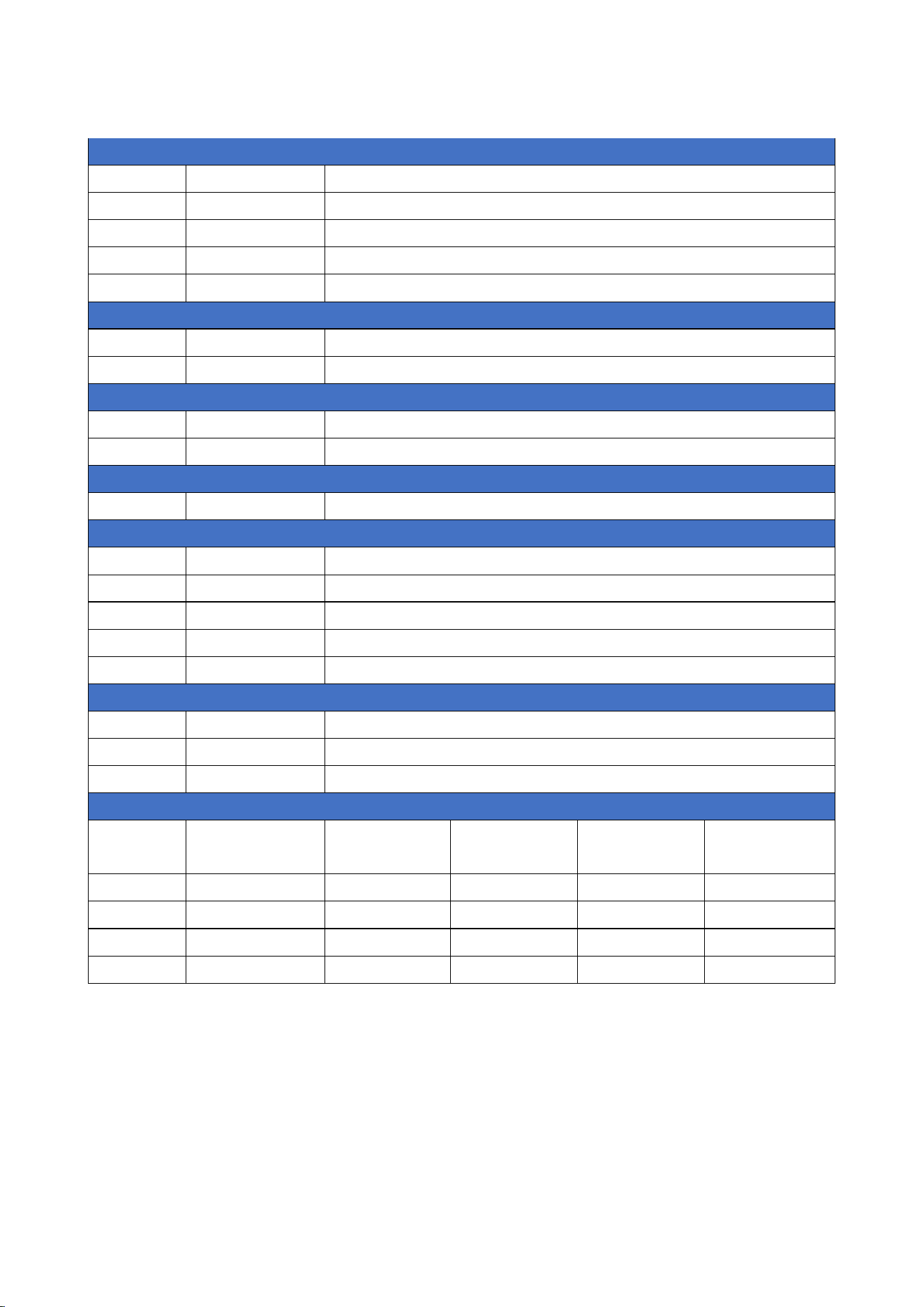
3.1 GPIO Recommended usage
Module
PIN N0.
NRF54LM20A
GPIO
Recommended usage
QSPI
K2
P2.00
QSPI D3
K1
P2.01
QSPI SCK
H2
P2.02
QSPI D0
G1
P2.03
QSPI D2
F2
P2.04
QSPI D1
E3
P2.05
QSPI CSN
TWI (Note: TWIM and TWIS must use clock pins for both SDA and SCL)
B9
P0.03
TWI
C10
P0.04
TWI
E7
P0.07
TWI
C1
P1.03
TWI
C3
P1.04
TWI
J7
P1.13
TWI
J9
P1.14
TWI
C7
P3.04
TWI
UARTE 00
K2
P2.00
RXD
H2
P2.02
TXD
F2
P2.04
CTS
E3
P2.05
RTS
UARTE 00
J3
P2.07
RXD
J1
P2.08
TXD
G3
P2.09
CTS
E5
P2.10
RTS
SPI 00
K2
P2.00
SPIM DCX
K1
P2.01
SPIM/SPIS SCK
H2
P2.02
SPIM/SPIS SDO
F2
P2.04
SPIM/SPIS SDI
E3
P2.05
SPIM CSN
SPI 00
L2
P2.06
SPIM/SPIS SCK
J3
P2.07
SPIM DCX
J1
P2.08
SPIM/SPIS SDO
G3
P2.09
SPIM/SPIS SDI
E5
P2.10
SPIM CSN
NFC
B5
P1.01
NFC1
A3
P1.02
NFC2
PWM
Port 1
PWM
Port 3
PWM
Clock Output
C10
P0.04
GRTC LF clock output (32.768KHZ)
Analog Input
B2
P1.31
AIN1
B1
P1.30
AIN2
D2
P1.29
AIN3
C3
P1.06
AIN6
C1
P1.03
AIN7
Radio (Direction Finding Antenna select GPIO)
K8
P1.16
Radio 1
J5
P1.20
Radio 5
K4
P1.21
Radio 6
Port Special function and characteristics
Port
Wakeup
source
Extra high
drive
Pin sense
/detect
GPIOTE
Maximum
speed(MHz)
P0
Yes
No
Yes
Yes
8
P1
Yes
No
Yes
Yes
8
P2
No
Yes
No
No
64
P3
Yes
No
Yes
Yes
8
11
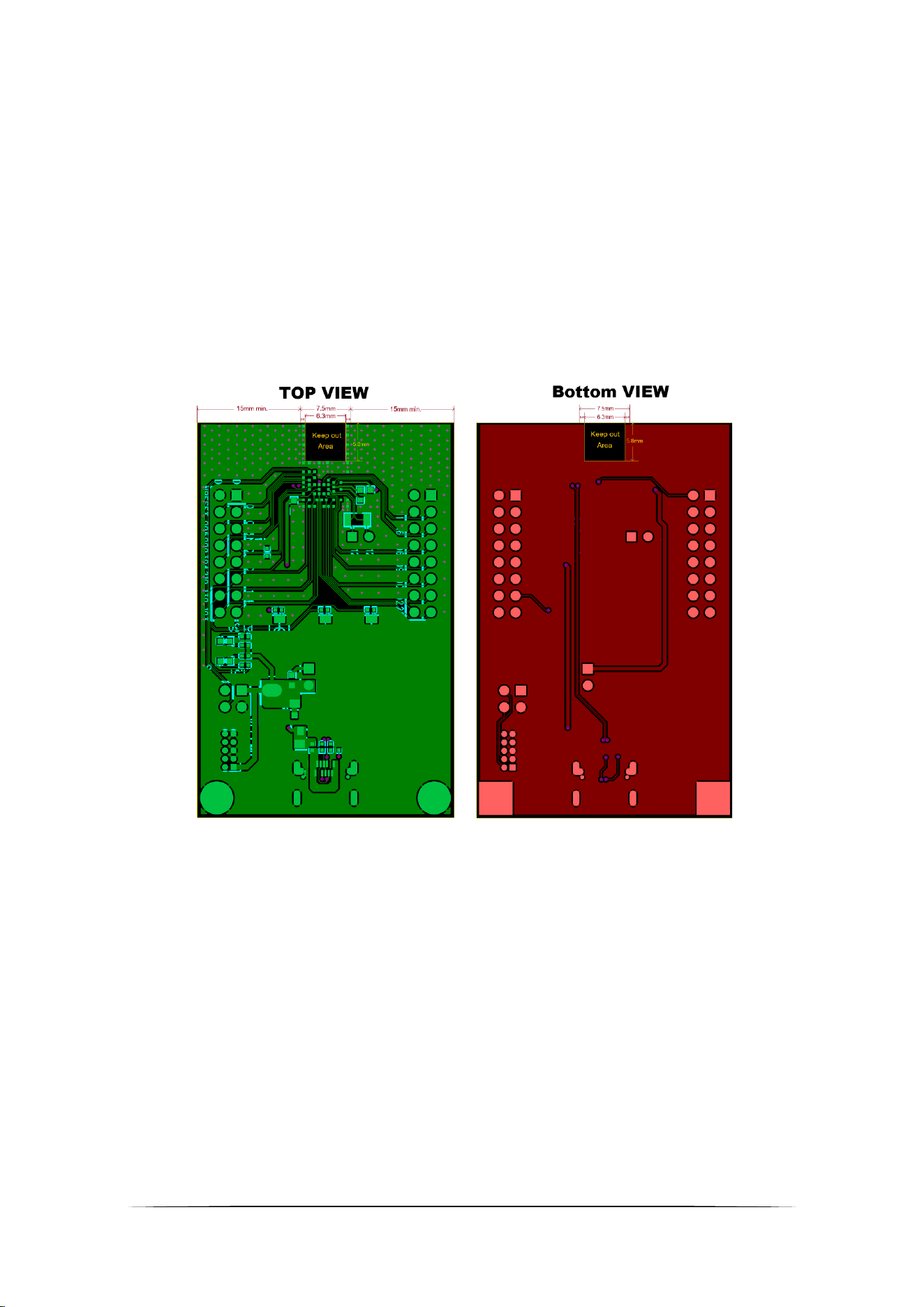
4 Layout design notes
4.1 Recommended RF layout and ground plane
It is recommended to place the module:
• In the center (horizontal) of any mother PCB edge, with GND planes to the left and right
• Keep out Area should be included in the corresponding position of the antenna in each layer.
• Add via hole around GND pads on the mother PCB as many as you can, especially on the four
corners and antenna area.
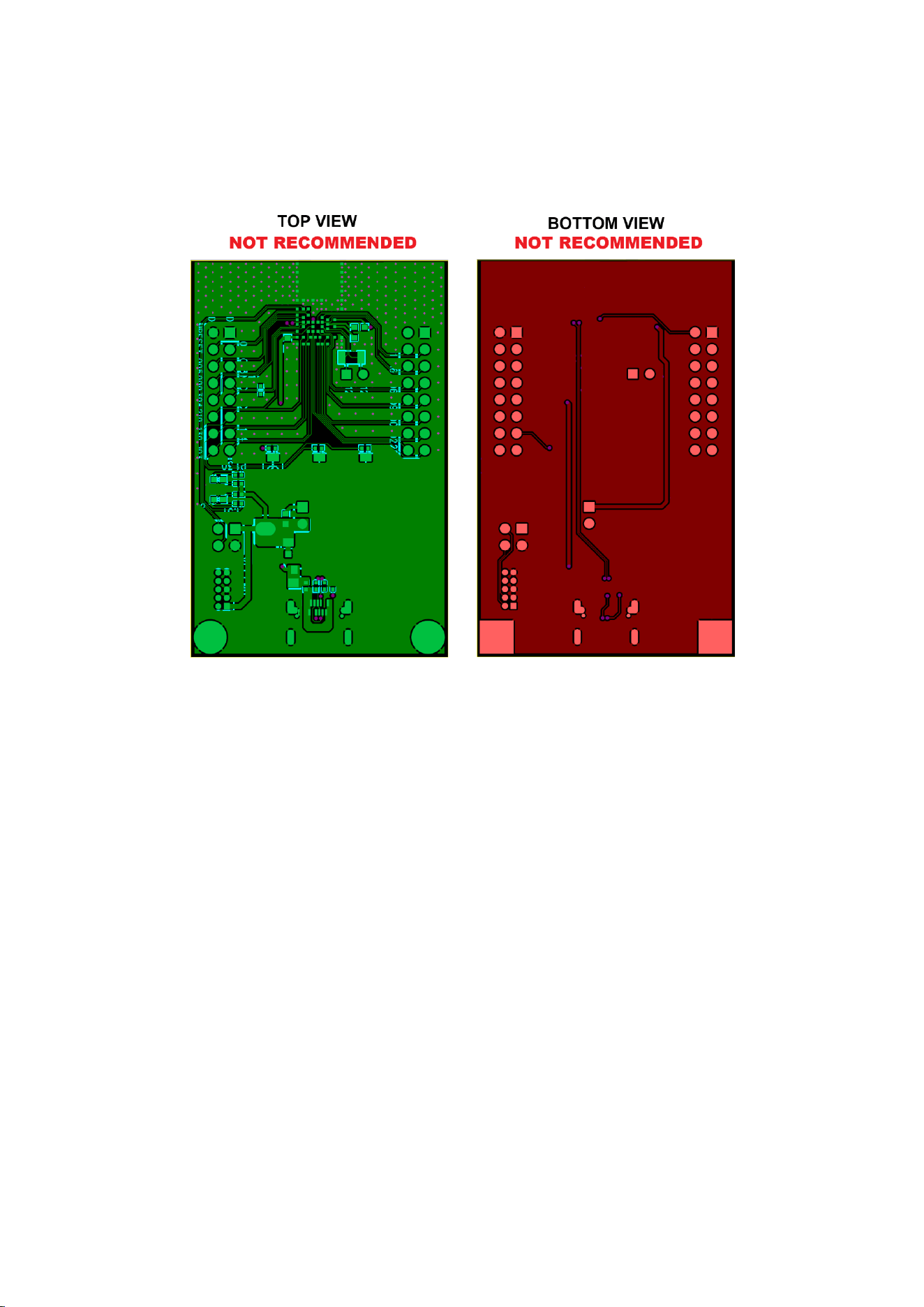
4.2 Not Recommended RF layout and ground plane
4.3 Antenna keep out when proximity to Metal
• The minimum safe distance for metals without seriously compromising the
antenna tuning is 4cm (bottom, top, left, right).
• Metal close to the antenna (bottom, top, left, right) will degrade RF
performance. Any metal closer than 2 cm will significantly degrade RF
performance.
13
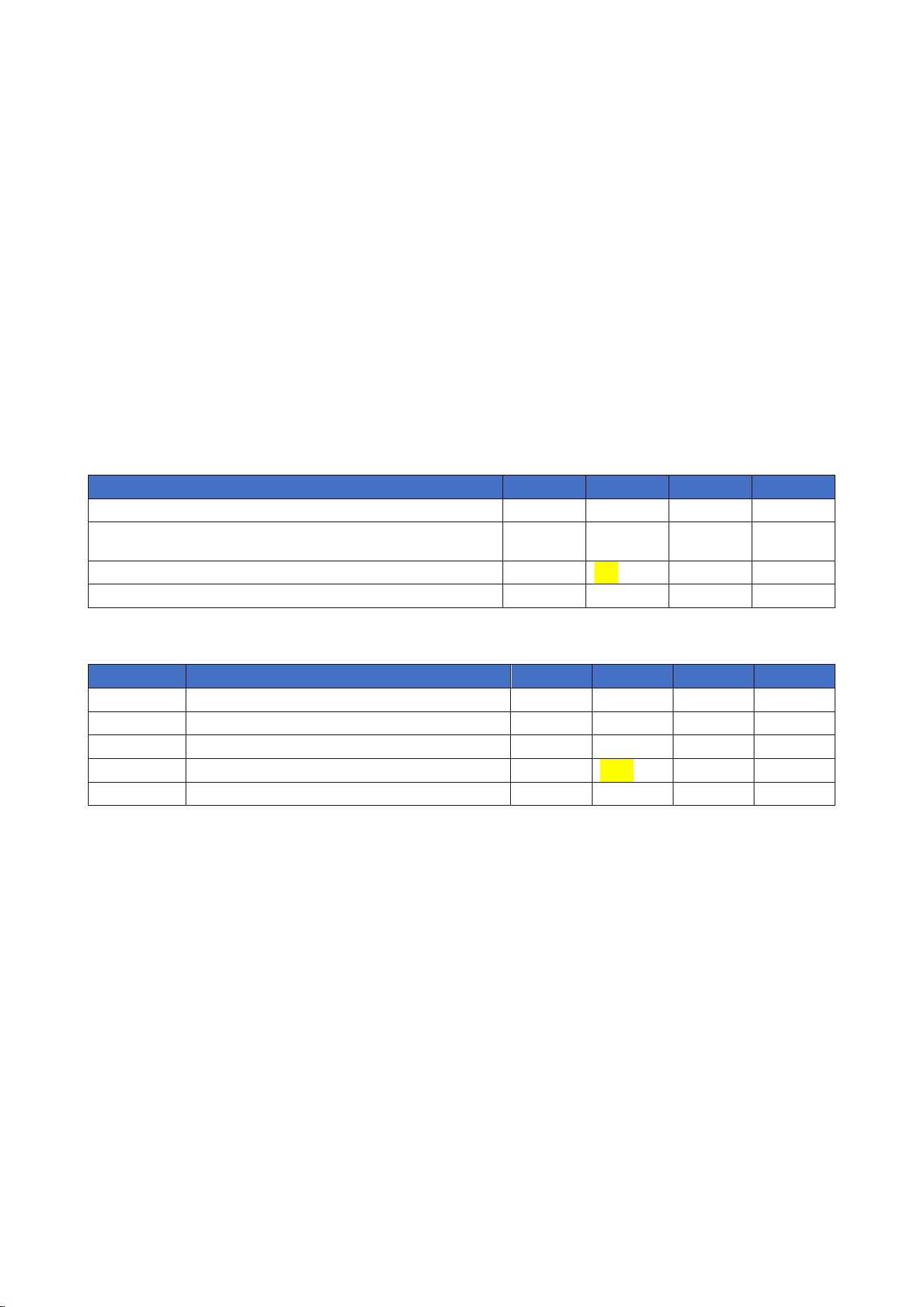
5.1 Operation Conditions
Parameter
Min.
Max.
Unit
Supply voltage
VDD
-0.3
+3.9
V
VSS
0
V
VBUS
-0.3
+6.0
V
I/O pin voltage
VI/O, VDD ≤3.6 V
-0.3
VDD+0.3
V
VI/O, VDD >3.6 V
3.9
V
Environmental
Storage temperature
-40
+125
°C
Recommended storage temperature<40°C
Recommended storage relative humidity <70%
MSL (moisture sensitivity level)
3
ESD HBM (human body model)
2
KV
ESD CDM (charged device model)
250
V
Flash memory
Endurance
10,000
Write/erase cycles
Retention
10 years at 85°C
5.2 System Clock
The MN54LMrequires two clocks, a high frequency clock and a low frequency clock.
MN54LM
• The high frequency clock (HFCLK)
HFCLK is provided on-module by a high-accuracy 32 MHz/±20 ppm crystal for radio and CPU
operation.
• The low frequency clock (LFCLK)
LFCLK can be provided internally by an RC oscillator (±250 ppm) with calibration, or externally by a
32.768 kHz crystal.
Internal 32.768 kHz RC oscillator (LFRC)
Description
Min.
Typ.
Max.
Unit
Nominal frequency
32.768
kHz
Frequency tolerance for LFRC after calibration
(calibration performed at least every 8 seconds)
±500
ppm
Run current for 32.768 kHz RC oscillator
0.7
uA
Startup time for 32.768 kHz RC oscillator
1000
us
External 32.768 kHz crystal oscillator (LFXO)
Parameter
Description
Min.
Typ.
Max.
Unit
Crystal frequency
32.768
kHz
Frequency tolerance requirement for BLE stack
±500
ppm
Frequency tolerance requirement for ANT stack
±50
ppm
Run current for 32.768 kHz crystal oscillator
0.23
uA
CL
Load capacitance
6
9
pF
An external crystal provides the lowest power consumption and greatest accuracy.
Using the internal RC oscillator with calibration provides acceptable performance for BLE stack at a
reduced cost and slight increase in power consumption.
15
5.3 Antenna information
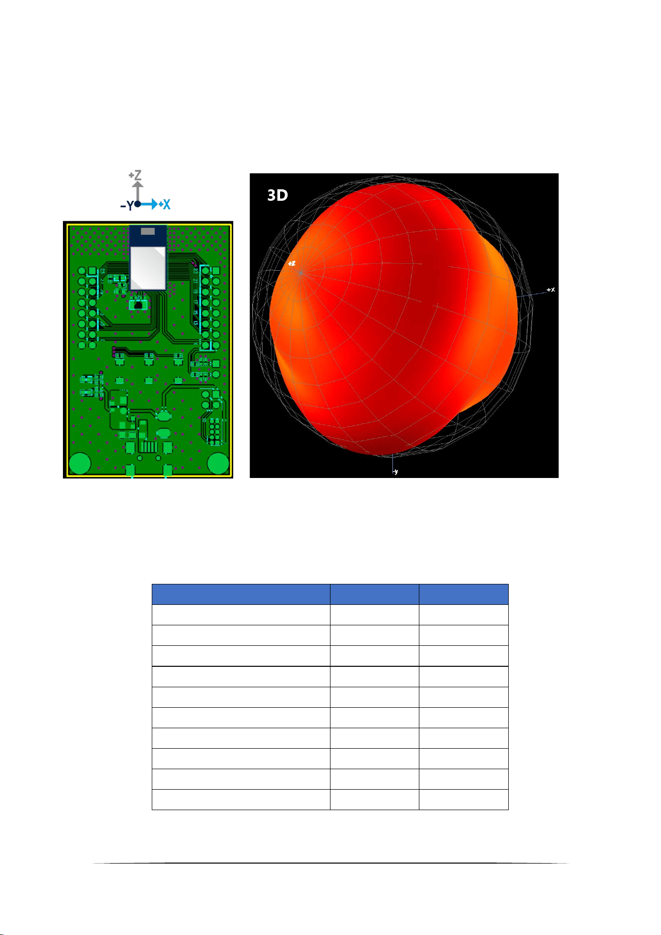
5.3.1 The orientation of Antenna
5.3.2 Antenna Gain and Efficiency
Frequency
Gain(dBi)
Efficiency
2400MHZ
-0.21
42
2410MHZ
0.22
45
2420MHZ
0.52
47
2430MHZ
0.92
50
2440MHZ
1.05
51
2450MHZ
0.87
50
2460MHZ
0.62
48
2470MHZ
0.43
44
2480MHZ
0.19
40
2490MHZ
-0.27
35
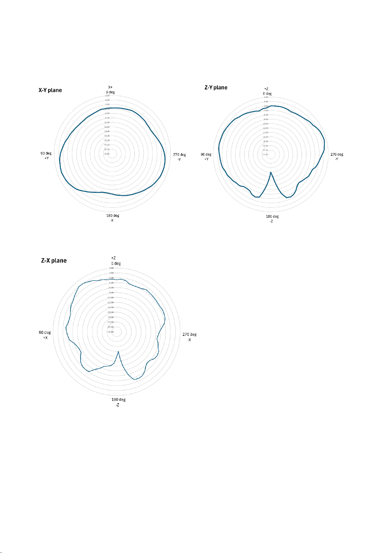
5.3.3 Antenna Pattern 2D
17
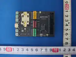
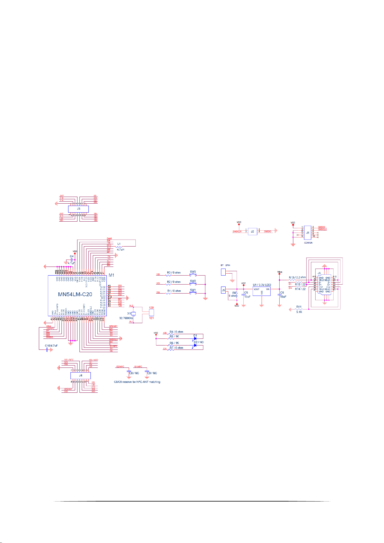
6. BN54LM-C20 evaluation board
BN54LM-C20 is a full-featured evaluation board for MN54LM-C20 that supports:
M1:MN54LM-C20 module
J6: USB Type C
J3/J4: Complete I/O pinout to headers
J1/J2: On-board programming and debugging interface
X1:32.768 kHz crystal
D1: One user LED
SW1/SW2/SW3: Three user buttons
C8/C9: NFC ANT matching
L1: DC-TO-DC power inductor
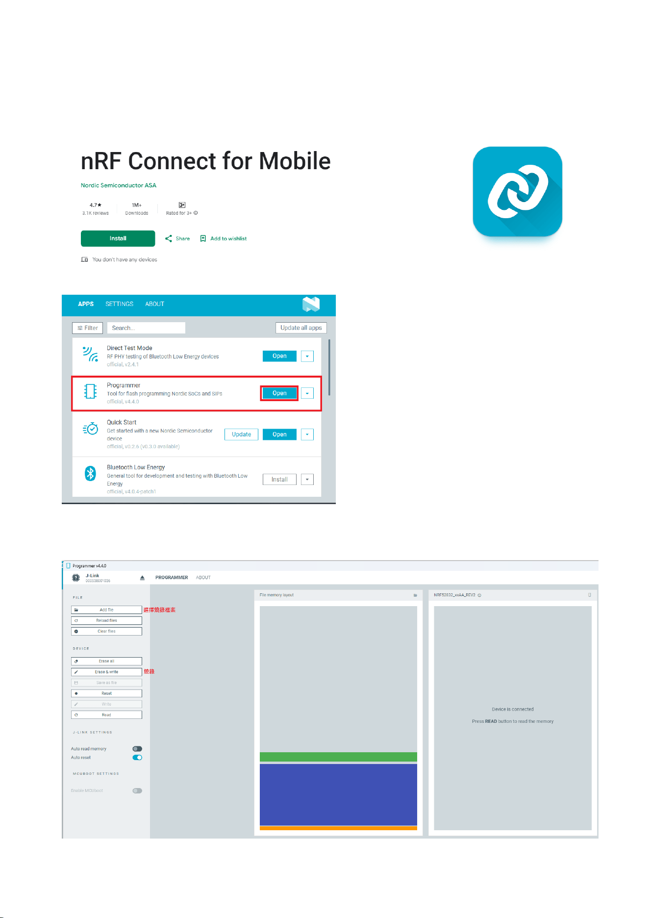
7. How to programming your code
7.1 Download NRFConnect for Desktop
7.2 Open programmer
7.3 chose your hex file

19
8.1 USA (FCC Certificate)
8.1.1 FCC ID and Labeling requirements
The MN54LM series hold full modular certification, are assigned the
FCC ID number: 2BLIDMN54LM
If the FCC ID is not visible when the module is installed inside OEM device, then the outside of
the finished product must also display a label referring to the enclosed module. The end product
must in any case be labelled on the exterior with:
Contains FCC ID: 2BLIDMN54LM
8.1.2 Federal Communication Commission Interference Statement:
This equipment has been tested and found to comply with the limits for a Class B digital device,
pursuant to Part 15 of the FCC Rules. These limits are designed to provide reasonable protection
against harmful interference in a residential installation.
This equipment generates, uses and can radiate radio frequency energy and, if not installed and
used in accordance with the instructions, may cause harmful interference to radio
communications. However, there is no guarantee that interference will not occur in a particular
installation. If this equipment does cause harmful interference to radio or television reception,
which can be determined by turning the equipment off and on, the user is encouraged to try to
correct the interference by one of the following measures:
. Reorient or relocate the receiving antenna.
. Increase the separation between the equipment and receiver.
. Connect the equipment into an outlet on a circuit different from that to which the receiver is
connected.
. Consult the dealer or an experienced radio/TV technician for help.
FCC Caution: To assure continued compliance, any changes or modifications not expressly
approved by the party responsible for compliance could void the user's authority to operate this
equipment. (Example - use only shielded interface cables when connecting to computer or
peripheral devices).
FCC Radiation Exposure Statement
This equipment complies with FCC RF radiation exposure limits set forth for an uncontrolled
environment. This equipment should be installed and operated with a minimum distance of 20
centimeters between the radiator and your body.

This transmitter must not be co-located or operating in conjunction with any other antenna or
transmitter.
The antennas used for this transmitter must be installed to provide a separation distance of at
least 20 cm from all persons and must not be co-located or operating in conjunction with any
other antenna or transmitter.
8.1.3 FCC Notice:
This device complies with Part 15 of the FCC Rules. Operation is subject to the following two
conditions:
(1) This device may not cause harmful interference, and (2) this device must accept any
interference received, including interference that may cause undesired operation.
8.1.4 RF Exposure Statement:
This module is approved for installation into mobile and/or portable host platforms.
This device is intended only for OEM integrators under the following conditions:
(1) The transmitter module may not be co-located with any other transmitter or antenna.
(If the condition above is met, further transmitter test will not be required.)
(2) The OEM integrator is still responsible for testing their end-product for any additional
compliance requirements required for satisfying RF Exposure compliance when this module
installed.
8.2 NCC Certificate (Taiwan)
8.2.1 NCC ID and Labeling requirements
MN54LM 系列依天線不同,可分為 4 種型式 , 認證為 4 個不同的 NCC ID
NCC logo and NCC ID
MN54LM-C : CCAH
MN54LM-P : CCAH
MN54LM-S : CCAH
MN54LM-U: CCAH

21
NCC 警語:
「取得審驗證明之低功率射頻器材,非經核准,公司、商號或使用者均不得擅自變更頻率、
加大功率或變更原設計之特性及功能。低功率射頻器材之使用不得影響飛航安全及干擾合法
通信;經發現有干擾現象時,應立即停用,並改善至無干擾時方得繼續使用。前述合法通
信,指依電信管理法規定作業之無線電通信。低功率射頻器材須忍受合法通信或工業、科學
及醫療用電波輻射性電機設備之干擾。」