
DATASHEET
TIANDONGLI
TECHNOLOGY
AB2036A
5.4 BLUETOOTH MODULE DA BLE TASHEET
VERSION 1.0
Shenzhen Tiandongli Technology Co., Ltd. @ All rights reserved

DATASHEET
1
Shenzhen Tiandongli Technology Co., Ltd. reserves the right to revise its products, documents and services at any time. To
minimize the risk of customers purchasing counterfeit products through unauthorized channels, customers shall obtain the latest
relevant information from our company before placing orders. Without the written permission of Shenzhen Tiandongli
Technology Co., Ltd., reproduction, transfer, distribution or storage of all contents in this document in any form is prohibited..
Revision Record
edition
date
take notes
author
1.0
2026/03/28
Initial Version
Zheng Yu
contact us
Shenzhen Tiandongli Technology Co., Ltd.
Website: https://www.tiandongli.cn

DATASHEET
2
catalogue
1 Introduction ........................................................................................................................................................................... 3
1.1 Overview ...................................................................................................................................................................... 3
1.2 Features .........................................................................................................................................................................3
1.3 Application ................................................................................................................................................................... 3
2 General Specifications ...........................................................................................................................................................4
3 Hardware Specifications .......................................................................................................................................................4
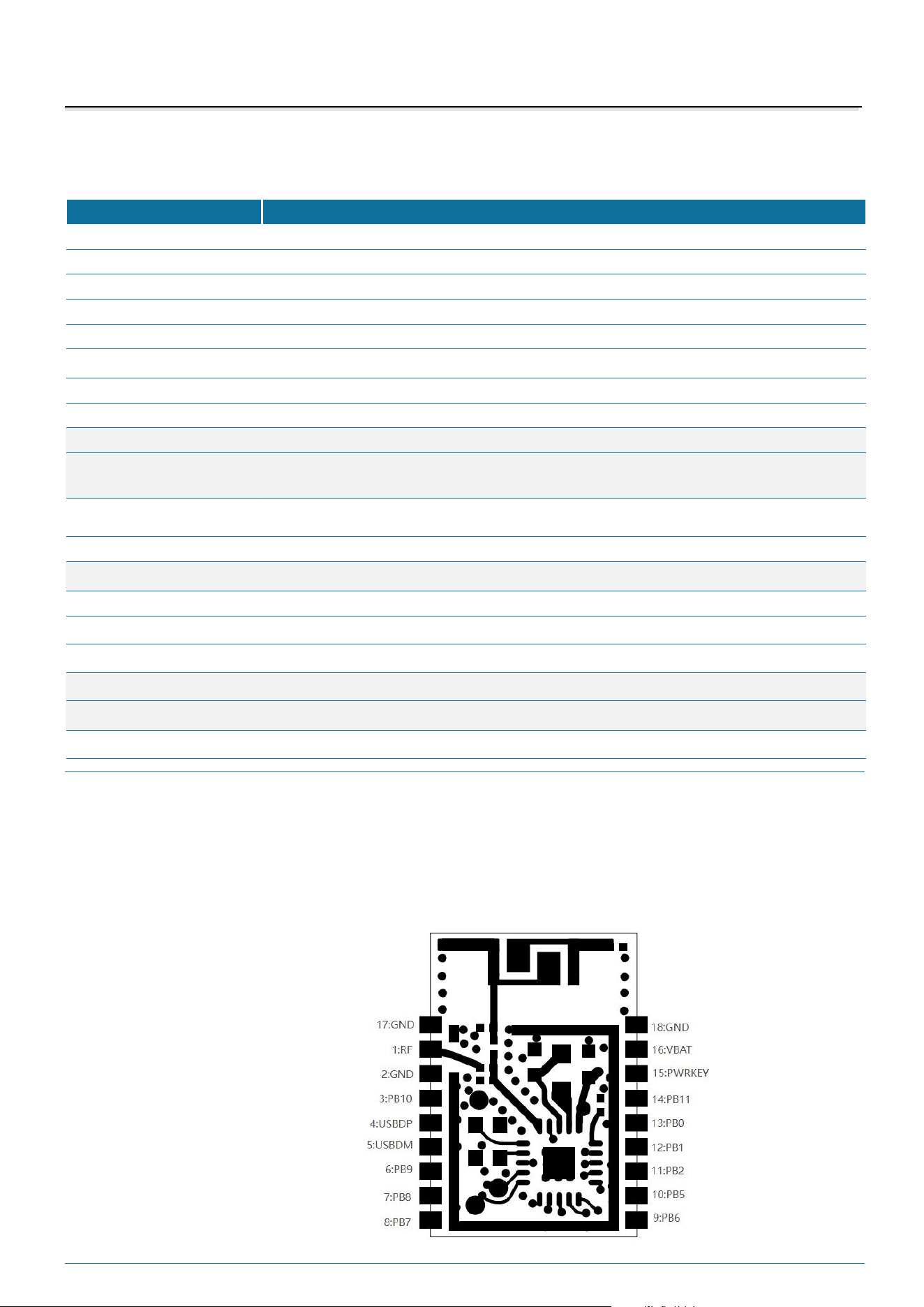
3.1 Pin Definition Diagram ................................................................................................................................................ 4
3.2 Pin Definition Explanation ...........................................................................................................................................5
4 Physical Interfaces .................................................................................................................................................................5
4.1 Universal Digital IO Port ............................................................................................................................................. 5
4.2 RF Interface .................................................................................................................................................................. 5
4.3 UART Interface ............................................................................................................................................................5
4.4 ADC Interface .............................................................................................................................................................. 6
5 Electrical Characteristics ......................................................................................................................................................6
5.1 Maximum Rated Value ................................................................................................................................................ 6
5.2 Recommended Working Conditions ............................................................................................................................7
6. Humidity sensitivity level & Anti-static level .................................................................................................................... 7
7 Reflow soldering .................................................................................................................................................................... 7
8 Module Structure Parameters ..............................................................................................................................................9
8.1 Physical Dimensions .................................................................................................................................................... 9
9 Hardware Design Recommendations ................................................................................................................................ 10
9.1 Welding Recommendations ....................................................................................................................................... 10
9.2 Layout Guidelines ...................................................................................................................................................... 10
9.3 Layout Guidelines ...................................................................................................................................................... 11
9.4 External Antenna ........................................................................................................................................................11
10 Product Packaging Information ...................................................................................................................................... 12

DATASHEET
3
1 Introduction
1.1 Overview
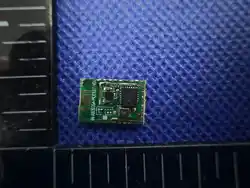
The AB2036A is a BLE Bluetooth 5.4 module developed by Shenzhen Tiandongli Technology Co., Ltd. This
module supports standard Bluetooth specifications and configuration profiles including HID, GATT, and ATT,
utilizing the UART serial port as its primary data transmission interface. Users can send AT commands through this
interface to query and modify module parameters, such as adjusting baud rates or changing Bluetooth names. For
detailed AT command formats and usage instructions, refer to the "Tiandongli Technology Bluetooth Serial Port
Command Set".
1.2 Features
•
BLE Bluetooth 5.4
•
Stamp hole encapsulation
•
Low power consumption
• Default transmission power: 0 dBm
• UART baud rate: 9600 bps (default), supports ranges from 1200 bps to 921.6 kbps
•
UART Hardware Interface
•
Supports serial port upgrade
• Supported Bluetooth profiles: GATT, ATT, GAP
•
Power consumption in operating mode (VDDIO_3V3 at 3.3 V)
• RX Mode: 12 mA @ 3.3 V, 0 dBm
• TX Mode: 13 mA @ 3.3 V, 0 dBm
•
Deep sleep mode: 2.1
μ
A (RTC wake-up + GPIO wake-up)
• Supports Bluetooth SIG Mesh
• Supports private mesh
1.3 Applications
•
Health and Medical Equipment
• Measurement and Monitoring System
•
mouse
• Bluetooth car key
• toy
• Lighting fixtures
• Wireless transmission for home appliances
DATASHEET
4
2 General Specifications
Table 1:
feature detailed information
model
AB2036A
Dimension
8.5mm(W) X 12.5mm(L) X 2.3mm(H)
Bluetooth Specifications
Bluetooth BLE 5.4
Working Voltage Range
3.3 ~ 4.2V
transmitting power Maximum: 9 dBm
sensitivity
-98dBm @1M BLE,-96.5dBm @2M BLE
frequency range
2.402GHz -2.480GHz ISM band
modulation mode
GFSK
Baseband crystal oscillator
24MHz
Frequency hopping and
channels
Radio frequency input
im
p
edance
50 ohm
N/A
s
Antenna Type PCB-Based Antenna
hardware interface
UART
protocol
HID, GATT, ATT
Other Features
Supports low power consumption
working temperature
-40°C to +80°C
Storage Temperature
-40°C to +105°C
humidity
10%–95% non-condensable
environment accord with RoHS
3 Hardware Specifications
Pinout Diagram (Top View)

DATASHEET
5
3.2 Pin Definition Explanation
Table 2:
pin
Pin Name
type
Pin Description
1
RF
ANT
antenna
2
GND
GND
Power Supply Location
3
PB10
I/O
Programmable Input/Output Pin
4
PB3
I/O
Programmable Input/Output Pin/USBDP
5
PB4
I/O
Programmable Input/Output Pin/USB DM
6
PB9
I/O
Programmable Input/Output Pin
7
PB8
I/O
Programmable Input/Output Pin
8
PB7
I/O
Programmable Input/Output Pin
9
PB6
I/O
Programmable Input/Output Pin
10
PB5
I/O
Programmable Input/Output Pin
11
PB2
I/O
Programmable Input/Output Pin
12
PB1
I/O
UART_TX
13
PB0
I/O
UART_RX
14
PB11
I/O
Programmable Input/Output Pin
15
PWRKEY
A
By default, it pulls up; short press to lower it below 0.7 V to trigger reset. The software
can be configured to disable the reset function.
16
VBAT
P
power input
17
GND
GND
Power Supply Location
18
GND
GND
Power Supply Location
4 Physical Interfaces
4.1 Universal Digital IO Port
The module integrates 12 universal GPIO ports. All GPIOs can be flexibly configured via software, supporting
functions such as button detection, LED driving, and interrupt signal output. Unused pins should remain unconnected to
external circuits. Each I/O pin can be independently configured for input or output mode.
4.2 RF Interface
• 2402–2480 MHz Bluetooth LE 5.4
• TX transmission power: -20 dBm to +9 dBm, maximum +9 dBm
•
RX Sensitivity: 1 M BLE sensitivity
–
98 dBm; 2 M BLE sensitivity
–
96.5 dBm (PER = 30.8%,37 bytes)
4.3 UART Interface
The module features a standardized UART serial interface with two pins
—
UART_TX (send) and UART_RX (receive)
—for bidirectional data transmission with other digital devices.
Table 3:
parameter
probable value
1200 baud (≤2%Error)
9600bps(≤1%Error)
Minimum
Baud rate, baud raterate, baud raterate
standard

DATASHEET
6
921600bps(≤1%Error)
Flow Control
RTS/CTS
Parity Bit
None, Odd or Even
Stop Bit Count
1
Data Bits Per Frame
8
4.4 ADC Interface
10-bit resolution ADC with 11 input channels, sampling rate up to 1MSPS
⚫ Supports single conversion mode or continuous mode
⚫ Supports DMA data reading functionality
⚫ Voice function, Sampling rate: 8K
⚫ Supports power supply voltage acquisition
⚫ Supports single-ended inputs for up to 11 channels
⚫ Data width is 10 bits, with an effective width of up to 9 bits
5 Electrical Characteristics
5.1 Maximum Rated Value
The following lists the power supply voltages and their absolute maximum rated values for both digital and analog
pins of the module. Exceeding these values may cause permanent damage. The average GPIO pin output current is
defined as the average current value flowing through any given pin over a 100 ms period. The total average GPIO pin
output current is defined as the average current value flowing through all corresponding pins over the same 100 ms
period. The maximum output current is defined as the peak current value flowing through any given pin.
Table 4:
parameter
least value
crest value
unit
V
IN
– I/O Power Voltage (VDDIO): -0.3 +3.6 V
V
IN
–
Analog/Digital Power Voltage (VDD): -0.3 +3.6
V
T
OT
-Operating Temperature
-40 +80 °C
T
ST
–
Storage Temperature
-40 +105
°
C
maximum

DATASHEET
7
5.2 Recommended Working Conditions
Table 5:
parameter
Min.
Typ.
Max
unit
V
IN
- Core Power Supply Voltage(VDD)
3.0 3.3 3.6 v
V
IN
-
I/O Supply Voltage (VDDIO) 3.0 3.3 3.6 v
6 Humidity Sensitivity Level & Anti-static Level
Table 6:
parameter
Value
Humidity Sensitivity Level Level 3
ESD Protection Grade
Human discharge pattern: Class 2
Machine Discharge Mode: Class-B
7 Reflow soldering
Before performing any reflow soldering, it is essential to ensure the module is packaged moisture-proof. The
packaging contains desiccant (to absorb moisture) and a humidity indicator card showing the dryness level
maintained during storage and transportation. If baking the module is required, refer to the table below and follow
the instructions specified in IPC/JEDEC J-STD-033.
Note: The tray must not be heated above 65
°
C. If using the high-temperature baking method listed in the
table (above 65
°
C), remove the module from the transport tray.
Any module that has been opened but does not contain the adhesive patch within the specified time frame
shall be repackaged, with effective desiccant and a temperature/humidity indicator card placed inside the
packaging. Under ambient conditions of 30 ° C/60% RH, MSL (Humidity-Sensitive Level) 3 modules shall not
remain exposed to air for more than 168 hours. The recommended baking duration and temperature are as follows:
Table 7:
MSL
Baking temperature:
125°C
Baking temperature: 90°C/
≤ 5% RH
Baking temperature: 40°C/
≤5% RH
saturated @
30°C/85%
Minimum
limit + 72
hours at
30 °C/60%
saturated @
30°C/85%
Minimum
limit + 72
hours at 30
°C/60%
saturated @
30°C/85%
Minimum
limit + 72
hours at 30
°
C/60%
3 9 hours 7 hours 33 hours 23 hours 13 days 9 days
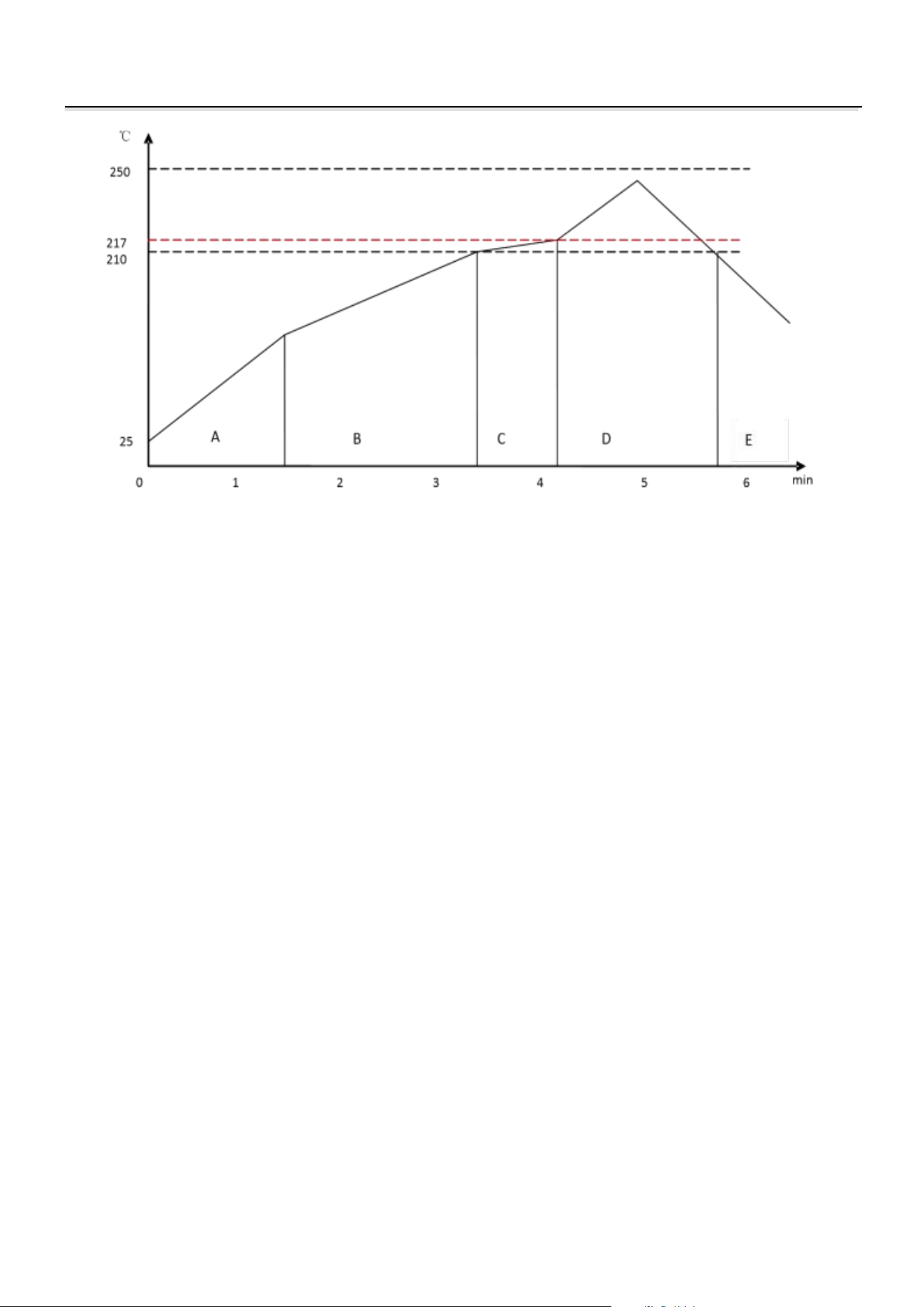
Surface-mount modules are designed for easy manufacturing, including reflow soldering onto the PCB
substrate. Ultimately, customers are responsible for selecting the appropriate solder paste and ensuring that the
furnace temperature during reflow meets the paste's specifications. Surface-mount modules comply with the J-
STD-020D1 standard for reflow soldering temperatures. The soldering configuration depends on various
parameters required for each application; the provided data serves solely as guidance for reflow soldering.
DATASHEET
8
Typical lead-free reflow process
Preheating Zone (A)
–
This zone is heated at a controlled rate, typically 0.5
–
2
°
C/s. Its purpose is to preheat the PCB
board and components to 120
–
150
°
C. During this stage, heat must be evenly distributed across the PCB board, and all
solvents must be completely removed to minimize thermal shock on the components.
Balancing Zone 1 (B) – At this stage, the flux becomes soft and uniformly encapsulates solder particles while
distributing them across the PCB board to prevent re-oxidation. As temperature rises and the flux liquefies, all activators
and rosin are activated, initiating removal of oxide films formed on both solder particles and the PCB surface. For this
zone, the recommended conditions are temperatures of 150
°
C to 210
°
C for 60 to 120 seconds.
Balancing Zone 2 (C) (optional) – To address the issue with upright components, it is recommended to maintain the
temperature at 210
–
217
°
C for approximately 20 to 30 seconds.
Reflow Zone (D)
–
The curve shown in the figure is designed for Sn/Ag
₃
.
₀
/Cu
₀
.
₅
and serves as a reference for
other lead-free solder formulations. The peak temperature should be sufficiently high to ensure adequate wetting, but not
so high as to cause component discoloration or damage. Excessive soldering time can promote intermetallic growth,
leading to brittle joints. The recommended peak temperature (Tp) ranges from 230 to 250 °C; when temperatures exceed
217
°
C, the soldering duration should be 30 to 90 seconds.
Cooling zone (E)
–
The cooling rate should be rapid to maintain small solder particles, resulting in a more durable
weld joint. The typical cooling rate is 4°C.
DATASHEET
9
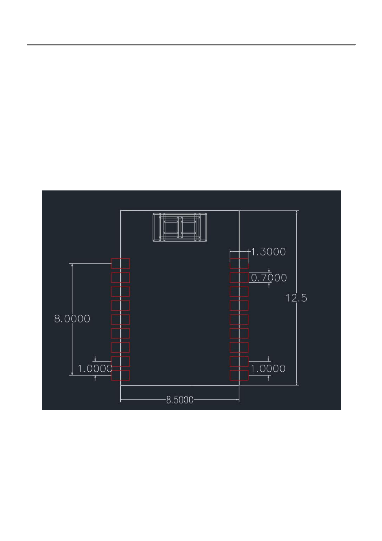
8 Module Structure Parameters
8.1 Physical Dimensions
• Unit: mm
Package Outline Drawing (Top View)
DATASHEET
10
9 Hardware Design Recommendations
9.1 Welding Recommendations
The AB2036A is compatible with industrial standard reflow curves for lead-free solder. The selected reflow
curve depends on the thermal mass of the entire assembled PCB, the heat transfer efficiency of the oven, and the
specific type of solder paste used. Refer to the data sheet of the particular solder paste for profile specifications.
Recommended reflow curves are provided for the following solder modules to ensure reliable solder joints and
performance after assembly. Since the appropriate reflow curve varies depending on process conditions and layout
design, optimal selection should be determined case-by-case. These recommendations serve as a starting point for
guidance.
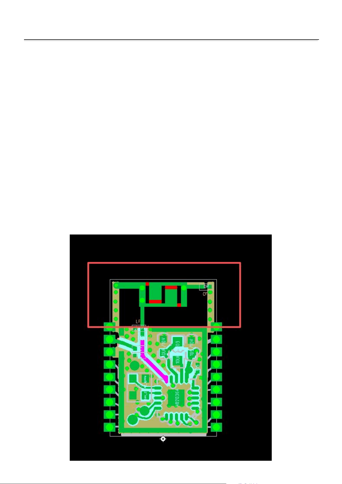
9.2 Layout Guidelines (Module Built-in Antenna)
It is strongly recommended to adopt proper layout practices to ensure optimal module performance. Placing
copper or any metal near the antenna can impair its performance and reduce efficiency. Metal shielding around the
antenna blocks signal radiation; therefore, metal enclosures should not be used with modules. Use multiple
grounding vias at the edges of ground areas. The following recommendations help prevent EMC issues in design:
Note that each design is unique, and this description does not cover all fundamental design principles (e.g.,
avoiding capacitive coupling between signal lines). These guidelines focus on mitigating EMC problems caused
by the module's RF components. Carefully consider these measures to avoid digital signal issues: Keep signal line
paths as short as possible. For signals entering inner layers via vias, always use grounding vias around pads and
place them symmetrically around signal traces. Critical signal paths should be routed entirely on inner PCB layers.
Sensitivity-sensitive traces should be surrounded by ground planes above and below. If this isn't feasible, ensure
the return path is minimized (e.g., using a ground trace adjacent to the signal line). Leave sufficient clearance on
the PCB beneath the module antenna.

DATASHEET
11
This device complies with part 15 of the FCC Rules. Operation is subject to the following two
conditions: (1) This device may not cause harmful interference, and (2) this device must
accept any interference received, including interference that may cause undesired operation.
NOTE: This equipment has been tested and found to comply with the limits for a Class B
digital device, pursuant to Part 15 of the FCC Rules. These limits are designed to provide
reasonable protection against harmful interference in a residential installation. This equipment
generates, uses and can radiate radio frequency energy and, if not installed and used in
accordance with the instructions, may cause harmful interference to radio communications.
However, there is no guarantee that interference will not occur in a particular installation. If
this equipment does cause harmful interference to radio or television reception, which can be
determined by turning the equipment off and on, the user is encouraged to try to correct the
interference by one or more of the following measures:-- Reorient or relocate the receiving
antenna.
-- Increase the separation between the equipment and receiver.
-- Connect the equipment into an outlet on a circuit different from that to which the receiver is
connected.
-- Consult the dealer or an experienced radio/TV technician for help.
Changes or modifications not expressly approved by the party responsible for compliance
could void the user's authority to operate the equipment.
The device has been evaluated to meet general RF exposure
requirement. The device can be
used in portable exposure condition without restriction.
1. This Modular Approval is limited to OEM installation only. The antenna
installation and operating configurations of this transmitter, including any applicable source-based time averaging duty
factor, antenna gain and cable loss must satisfy MPE categorical Exclusion Requirements.
2. The EUT is exempt from SAR measurement and must not transmit simultaneously with any other antenna or
transmitter.
3. A label with the following statements must be attached to the host end product: This device contains FCC ID:
2BWTD-TDLGDBLE001.
4. To comply with FCC regulations limiting both maximum RF output power and human exposure to RF radiation,
maximum antenna gain (including cable loss) must not exceed:
-0. 58 dBi
5. This module must not transmit simultaneously with any other antenna or transmitter
6. The host end product must include a user manual that clearly defines operating requirements and conditions that
must be observed to ensure compliance with current FCC RF exposure guidelines.
For portable devices, in addition to the conditions 3 through 6 described above, a separate approval is required to
satisfy the SAR requirements of FCC Part 2.1093.
If the device is used for other equipment that separate approval is required for all other operating configurations,
including portable configurations with respect to 2.1093 and different antenna configurations.
For this device, OEM integrators must be provided with labeling instructions of finished products.
Please refer to KDB784748 D01 v07, section 8. Page 6/7 last two paragraphs:
A certified modular has the option to use a permanently affixed label, or an electronic label. For a permanently affixed
label, the module must be labeled with an FCC ID - Section 2.926 (see 2.2 Certification (labeling requirements) above)
. The OEM manual must provide clear instructions explaining to the OEM the labeling requirements, options and OEM
user manual instructions that are required (see next paragraph).
For a host using a certified modular with a standard fixed label, if (1) the module’s FCC ID is not visible when
installed in the host, or (2) if the host is marketed so that end users do not have straightforward commonly used
methods for access to remove the module so that the FCC ID of the module is visible; then an additional permanent
label referring to the enclosed module: “Contains Transmitter Module FCC ID: 2BWTD-TDLGDBLE001” or “
Contains FCC ID: 2BWTD-TDLGDBLE001” must be used. The host OEM user manual must also contain clear
instructions on how end users can find and/or access the module and the FCC ID.
The final host / module combination may also need to be evaluated against the FCC Part 15B criteria for unintentional
radiators in order to be properly authorized for operation as a Part 15 digital device.In cases where the manual is
provided only in a form other than paper, such as on a computer disk or over the Internet, the information required by
this section may be included in the manual in that alternative form, provided the user can reasonably be expected to
have the capability to access information in that form.
data book
12
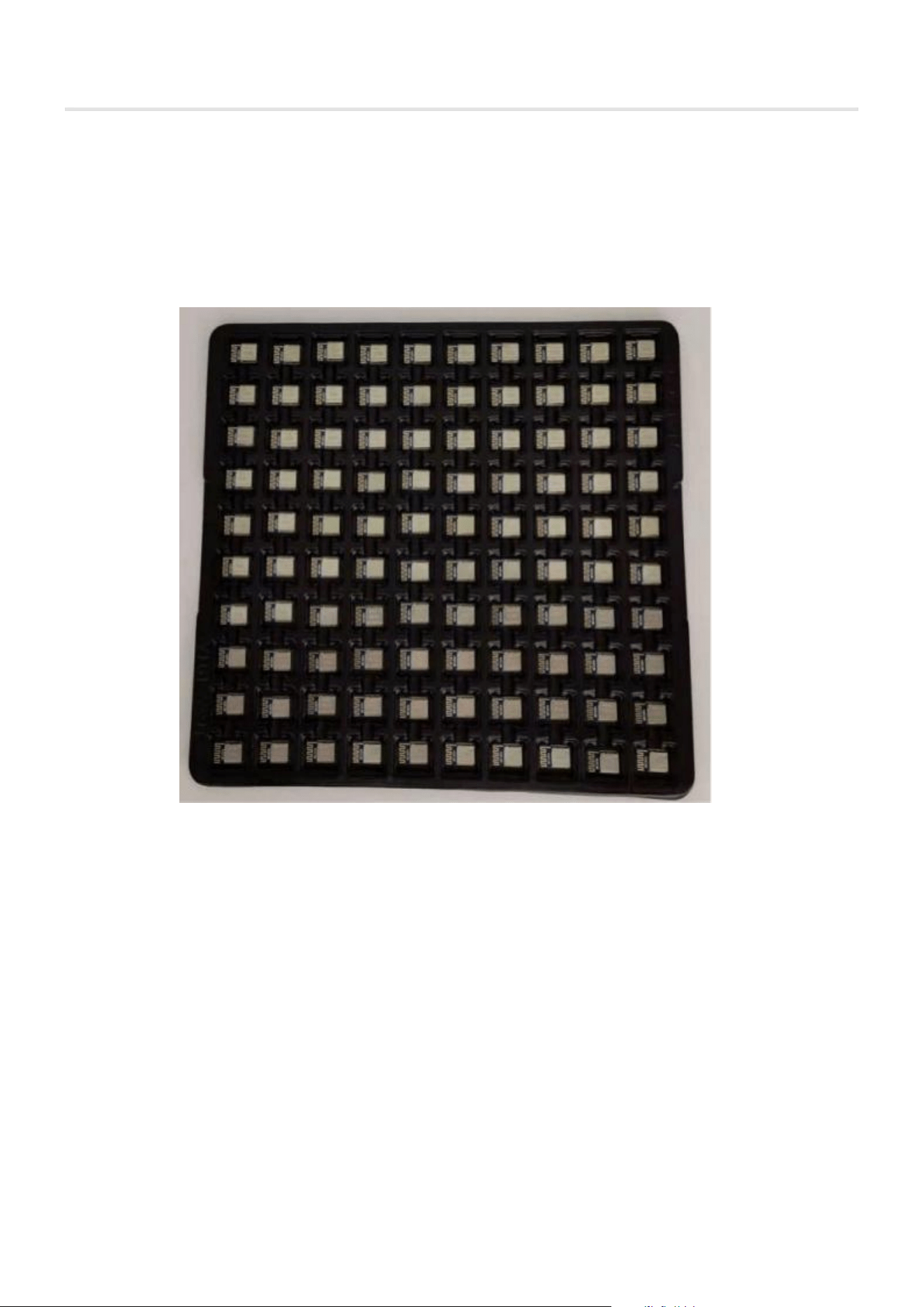
10 Product Packaging Information
Tape & Tray Packaging
Tray Dimension: 270mm × 220mm
100 pieces per tray
Minimum Order Packaging Quantity: 2000 pieces
Translation Note
1. All electronic/Bluetooth industry terms follow TI/Nordic official BLE datasheet standard
expression;
2. Standards such as IPC/JEDEC, RoHS, AFH, GFSK retain original English naming;
3. Pin functions, electrical parameters, reflow process sections fully conform to international
hardware specification writing norms;
4. Company name "添动力科技" unified as Tiandongli Technology for foreign customer
communication;
5. Tables, section numbering, document structure fully consistent with the original Chinese file.