

Contents
Contents
1. Overview . . . . . . . . . . . . . . . . . . . . . . . . . . . . . . . . . . . . . . . . . . . . . . . . . . . . . . 2
1.1. Features . . . . . . . . . . . . . . . . . . . . . . . . . . . . . . . . . . . . . . . . . . . . . . . . . . . . . . . . . . . . 2
1.2. Scope of applications . . . . . . . . . . . . . . . . . . . . . . . . . . . . . . . . . . . . . . . . . . . . . . . 3
2. Module interfaces . . . . . . . . . . . . . . . . . . . . . . . . . . . . . . . . . . . . . . . . . . . . . 4
2.1. Dimensions and footprint . . . . . . . . . . . . . . . . . . . . . . . . . . . . . . . . . . . . . . . . . . 4
2.2. Pinout . . . . . . . . . . . . . . . . . . . . . . . . . . . . . . . . . . . . . . . . . . . . . . . . . . . . . . . . . . . . . . . 4
3. Electrical parameters . . . . . . . . . . . . . . . . . . . . . . . . . . . . . . . . . . . . . . . . . . 8
3.1. Absolute electrical parameters . . . . . . . . . . . . . . . . . . . . . . . . . . . . . . . . . . . . . 8
3.2. Normal operating conditions . . . . . . . . . . . . . . . . . . . . . . . . . . . . . . . . . . . . . . . 8
3.3. Power consumption during continuous transmission and
reception . . . . . . . . . . . . . . . . . . . . . . . . . . . . . . . . . . . . . . . . . . . . . . . . . . . . . . . . . . . 9
3.4. Operating current . . . . . . . . . . . . . . . . . . . . . . . . . . . . . . . . . . . . . . . . . . . . . . . . . 11
4. RF parameters . . . . . . . . . . . . . . . . . . . . . . . . . . . . . . . . . . . . . . . . . . . . . . . 13
4.1. Basic RF features . . . . . . . . . . . . . . . . . . . . . . . . . . . . . . . . . . . . . . . . . . . . . . . . . 13
4.2. Transmitter (TX) performance . . . . . . . . . . . . . . . . . . . . . . . . . . . . . . . . . . . . 13
4.3. Receiver (RX) performance . . . . . . . . . . . . . . . . . . . . . . . . . . . . . . . . . . . . . . . 17
5. Antenna information . . . . . . . . . . . . . . . . . . . . . . . . . . . . . . . . . . . . . . . . . 20
5.1. Antenna type . . . . . . . . . . . . . . . . . . . . . . . . . . . . . . . . . . . . . . . . . . . . . . . . . . . . . . 20
5.2. Antenna interference reduction . . . . . . . . . . . . . . . . . . . . . . . . . . . . . . . . . . . 20
6. Packing and production instructions . . . . . . . . . . . . . . . . . . . . . . . . . 21
6.1. Mechanical dimensions . . . . . . . . . . . . . . . . . . . . . . . . . . . . . . . . . . . . . . . . . . . 21
6.2. Recommended PCB footprint . . . . . . . . . . . . . . . . . . . . . . . . . . . . . . . . . . . . . 22
6.3. Production instructions . . . . . . . . . . . . . . . . . . . . . . . . . . . . . . . . . . . . . . . . . . . 23
6.4. Recommended oven temperature curve . . . . . . . . . . . . . . . . . . . . . . . . . 26
6.5. Storage conditions . . . . . . . . . . . . . . . . . . . . . . . . . . . . . . . . . . . . . . . . . . . . . . . . 28
7. MOQ and packaging information . . . . . . . . . . . . . . . . . . . . . . . . . . . . . 29
8. Appendix: Statement . . . . . . . . . . . . . . . . . . . . . . . . . . . . . . . . . . . . . . . . . 30
I

1Overview
The T7-2S module is a Wi-Fi and Bluetooth Low Energy (LE) combo dual-band Wi-
Fi 6 module developed by Tuya Smart. It consists of a highly integrated RF chip,
T7, and a few peripheral components, with built-in Wi-Fi and Bluetooth network
protocol stacks and various library functions.
1 / 33

1Overview
1. Overview
The module is built around a low-power Armv8-MC1 MCU with 512 KB SRAM,
built-in 4 MB ash memory, and various peripheral resources.
T7-2S is a real-time operating system (RTOS), integrated with all Wi-Fi MAC and
TCP/IP libraries. All these resources can help you develop your own embedded Wi-
Fi products.
1.1. Features
• Built-in low-power Armv8-MC1 CPU that also acts as an application processor.
• Clock rate of up to 240 MHz.
• Operating voltage: 3.3V.
• Peripherals: 5 PWM pins, 1 UART (user), and 1 ADC pin.
• Wi-Fi connectivity
• IEEE 802.11a/b/g/n/ac/ax 1x1, 2.4 GHz and 5 GHz.
• The maximum output power is +18 dBm for IEEE 802.11b and +16 dBm for
• Support security protocols, including WPA2, WPA2 PSK (AES), and WPA3.
802.11a transmission.
• Support STA, AP, and STA + AP combo working modes. Except for UNII-2A/2C.
• Two pairing modes are supported, namely Bluetooth and AP mode. Both modes
are suitable for pairing with Android and iOS mobile phones.
• Onboard PCB antenna with a gain of 1.91 dBi at 2.4 GHz, and 1.53 dBi at 5
GHz.
• Operating temperature range: −40°C to +85°C.
• Bluetooth connectivity
• Support Bluetooth 6.0.
• Up to +6.5 dBm output power.
• Onboard PCB antenna with a gain of 1.91 dBi at 2.4 GHz, and sharing the same
antenna with Wi-Fi.
• Operating temperature range: −40°C to +85°C.
2 / 33

2.2Module interfaces
1.2. Scope of applications
• Smart building
• Smart home and electrical appliance
• Smart socket and light
• Industrial wireless control
• Baby monitor
• IP camera
• Smart bus
3 / 33
2.3Module interfaces
2. Module interfaces
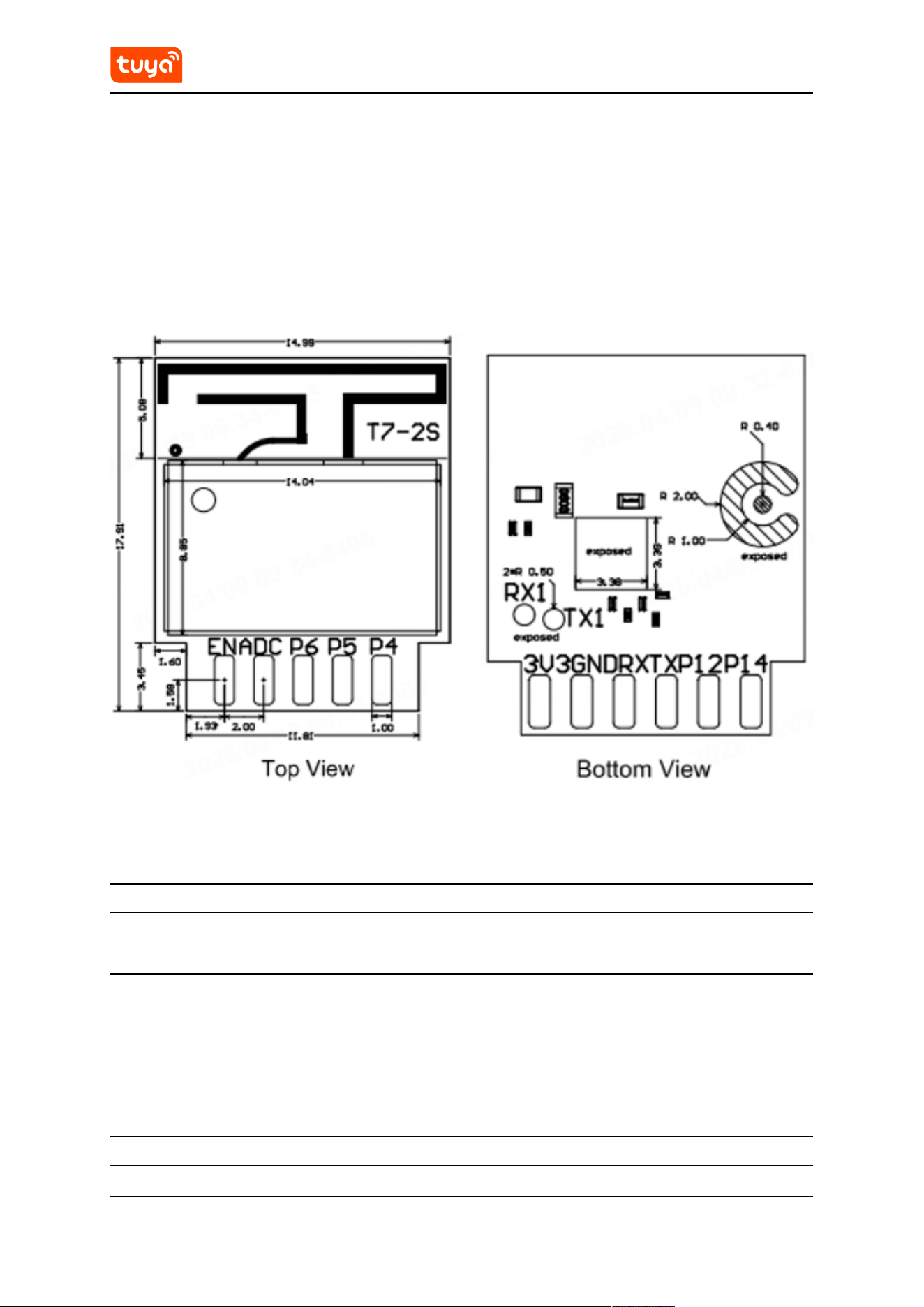
2.1. Dimensions and footprint
The T7-2S dimensions are 14.99±0.35 mm (W) × 17.91±0.35 mm (L) × 2.8±0.15
mm (H).
The gure below shows the dimensions of the T7-2S module.
2.2. Pinout
Pin Symbol I/O type Feature
1 3V3 P
Power supply pin
(3.3 V).
2 P4 I/O
GPIO_4, which
supports hardware
PWM,
corresponding to
Pin 19 on the IC.
3 GND P Ground pin.
4 / 33

3.3Electrical parameters
Pin Symbol I/O type Feature
4 P5 I/O
GPIO_5, which
supports hardware
PWM,
corresponding to
Pin 18 on the IC.
5 RX0 I/O
GPIO_10, which
can be reused as
the UART0_RXD
pin for serial
communication
and rmware
ashing,
corresponding to
Pin 24 on the IC.
6 P6 I/O
GPIO_6, which
supports hardware
PWM,
corresponding to
Pin 17 on the IC.
7 TX0 I/O
GPIO_11, which
can be reused as
the UART0_TXD
pin for serial
communication
and rmware
ashing,
corresponding to
Pin 25 on the IC.
5 / 33

3.3Electrical parameters
Pin Symbol I/O type Feature
8 ADC I/O
GPIO_7, with ADC
feature and 0 to
3.3V input voltage
range,
corresponding to
Pin 16 on the IC.
9 P12 I/O
GPIO_12, which
supports hardware
PWM,
corresponding to
Pin 26 on the IC.
10 CEN I/O
The enable pin
that is active low.
The module has
pulled up the high
level, and users
can control this
pin externally.
11 P14 I/O
GPIO_14, which
supports hardware
PWM,
corresponding to
Pin 36 on the IC.
6 / 33

3.3Electrical parameters
Pin Symbol I/O type Feature
TP2 TX1 I/O
GPIO_1, which can
be reused as the
UART1_Log_TXD
pin to send logs.
After pulling it
low, it will enter
ATE mode when
powered on. It can
be congured as a
normal GPIO,
corresponding to
Pin 20 on the IC.
TP3 RX1 I/O
GPIO_0, which can
be reused as the
UART1_Log_RXD
pin to receive
logs. It can be
congured as a
normal GPIO,
corresponding to
Pin 21 on the IC.
P indicates the power pin, and I/O indicates the input and output pin.
7 / 33

3.3Electrical parameters
3. Electrical parameters
3.1. Absolute electrical parameters
Parameter Description
Minimum
value
Maximum
value
Unit
Ts
Storage
temperature
−40 125 °C
VBAT
Supply
voltage
3 3.6 V
Electrostatic
discharge
voltage
(human body
model)
TAMB-25°C - 2 kV
Electrostatic
discharge
voltage
(machine
model)
TAMB-25°C - 0.5 kV
3.2. Normal operating conditions
Parameter Description
Minimum
value
Typical
value
Maximum
value
Unit
Ta
Operating
temperature
−40 - 85 °C
VBAT
Supply
voltage
3 3.3 3.6 V
VIL
I/O low-
level input
−0.3 - 0.3 VIO V
VIH
I/O high-
level input
0.7 VIO - VIO + 0.3 V
8 / 33

4.3RF parameters
Parameter Description
Minimum
value
Typical
value
Maximum
value
Unit
VOL
I/O low-
level
output
- - 0.1 VIO V
VOH
I/O high-
level
output
0.8 VIO - - V
Imax
I/O drive
current
- - 12 mA
3.3. Power consumption during continuous transmission and
reception
2.4 GHz transmission and reception
Work
state
Mode Rate
Transmit/
Receive
power
Typical
value
Unit
Transmit 802.11b 11 Mbit/s +18 dBm 328 mA
Transmit 802.11g 6 Mbit/s +17 dBm 310 mA
Transmit
802.11n-
HT20
MCS0 +16 dBm 294 mA
Transmit
802.11n-
HT40
MCS0 +13 dBm 246 mA
Transmit
802.11ax-
HE20
MCS0 +13 dBm 248 mA
Receive 802.11b 11 Mbit/s
Continuous
reception
45 mA
Receive 802.11g 6 Mbit/s
Continuous
reception
45 mA
Receive
802.11n-
HT20
MCS0
Continuous
reception
45 mA
Receive
802.11n-
HT40
MCS0
Continuous
reception
45 mA
9 / 33

4.4RF parameters
Work
state
Mode Rate
Transmit/
Receive
power
Typical
value
Unit
Receive
802.11ax-
HE20
MCS0
Continuous
reception
45 mA
5 GHz transmission and reception
Work
state
Mode Rate
Transmit/
Receive
power
Typical
value
Unit
Transmit 802.11a 6 Mbit/s +16 dBm 320 mA
Transmit
802.11n-
HT20
MCS0 +15 dBm 300 mA
Transmit
802.11n-
HT40
MCS0 +13 dBm 280 mA
Transmit
802.11ac-
VHT20
MCS0 +13 dBm 280 mA
Transmit
802.11ax-
HE20
MCS0 +13 dBm 280 mA
Receive 802.11a 6 Mbit/s
Continuous
reception
48 mA
Receive
802.11n-
HT20
MCS0
Continuous
reception
48 mA
Receive
802.11n-
HT40
MCS0
Continuous
reception
48 mA
Receive
802.11ac-
VHT20
MCS0
Continuous
reception
48 mA
Receive
802.11ax-
HE20
MCS0
Continuous
reception
48 mA
The above data is based on the module being powered by a DC regulated
power supply at 3.3V and operating in continuous transmission mode with a
100% duty cycle. The test data varies slightly between dierent modules.
10 / 33

4.4RF parameters
3.4. Operating current
Operating
mode
Status (Ta =
25°C)
Average
value
Max
(Typical)
value
Unit
Pairing over
AP
The module is
in AP mode.
The Wi-Fi
network
status
indicator
blinks slowly.
48 486 mA
Pairing over
Bluetooth
The module is
pairing over
Bluetooth.
The network
status
indicator
blinks quickly.
48 480 mA
Idle mode
The module is
connected to
the cloud and
idle. The
network
status
indicator is
steady on.
45 468 mA
11 / 33

4.5RF parameters
Working mode
The module is
connected to
the cloud and
working. The
network
status
indicator is
steady on.
45 472 mA
Weakly
connected
mode
The module is
operating in a
weak wireless
signal
network. The
network
status
indicator is
steady o.
48 476 mA
Disconnected
mode
The module is
disconnected
from the
cloud. The
network
status
indicator is
steady o.
48 460 mA
The above data is based on the module being powered by a DC regulated
power supply at 3.3V, utilizing the Tuya general rmware v1.0.1. The test
data varies slightly between dierent modules using the same rmware.
12 / 33

4.5RF parameters
4. RF parameters
4.1. Basic RF features
Parameter Description
Operating frequency
2.412 to 2.484 GHz (Ch1-11 for US/CA
and Ch1-13 for EU/CN), 5.180 to 5.825
GHz
Wi-Fi standard
IEEE 802.11a/b/g/n/ac/ax (Ch1-11 for
US/CA, Ch1-13 for EU/CN)
Bluetooth standard Bluetooth LE 6.0
Data transmission rate
• IEEE 802.11b: 1, 2, 5.5, and 11 Mbit/
s
• IEEE 802.11a/g: 6, 9, 12, 18, 24, 36,
48, and 54 Mbit/s
• IEEE 802.11n: HT20 MCS0-7 and
HT40 MCS0-7
• IEEE 802.11ac: VHT20 MCS0-7
• IEEE 802.11ax: HE20 MCS0-7
• Bluetooth 6.0: 1 Mbit/s and 2 Mbit/s
Antenna type
Onboard PCB antenna with a gain of
1.91 dBi at 2.4 GHz, and 1.53 dBi at 5
GHz
4.2. Transmitter (TX) performance
2.4 GHz continuous transmission performance
Parameter
Minimum
value
Typical value
Maximum
value
Unit
13 / 33

5.3Antenna information
Parameter
Minimum
value
Typical value
Maximum
value
Unit
RF average
output power,
802.11b CCK
mode, 1 Mbit/
s
- 18 - dBm
RF average
output power,
802.11b CCK
mode, 11
Mbit/s
- 18 - dBm
RF average
output power,
802.11g
OFDM mode,
6 Mbit/s
- 17 - dBm
RF average
output power,
802.11g
OFDM mode,
54 Mbit/s
- 16 - dBm
RF average
output power,
802.11n HT20
mode, MCS0
- 16 - dBm
RF average
output power,
802.11n HT20
mode, MCS7
- 15 - dBm
14 / 33

5.3Antenna information
Parameter
Minimum
value
Typical value
Maximum
value
Unit
RF average
output power,
802.11n HT40
mode, MCS0
- 13 - dBm
RF average
output power,
802.11n HT40
mode, MCS7
- 12 - dBm
RF average
output power,
802.11ax
HE20 mode,
MCS0
- 13 - dBm
RF average
output power,
802.11ax
HE20 mode,
MCS7
- 12 - dBm
RF average
output power,
Bluetooth LE
6.0, 1 Mbit/s
and 2 Mbit/s
- 6.5 - dBm
Frequency
error
−10 - 10 ppm
5 GHz continuous transmission performance
Parameter
Minimum
value
Typical value
Maximum
value
Unit
15 / 33

5.3Antenna information
Parameter
Minimum
value
Typical value
Maximum
value
Unit
RF average
output power,
5G-802.11a
mode, 6 Mbit/
s
- 16 - dBm
RF average
output power,
5G-802.11a
mode, 54
Mbit/s
- 15 - dBm
RF average
output power,
5G-802.11n
HT20 mode,
MCS0
- 15 - dBm
RF average
output power,
5G-802.11n
HT20 mode,
MCS7
- 14 - dBm
RF average
output power,
5G-802.11n
HT40 mode,
MCS0
- 13 - dBm
RF average
output power,
5G-802.11n
HT40 mode,
MCS7
- 12 - dBm
16 / 33

5.3Antenna information
Parameter
Minimum
value
Typical value
Maximum
value
Unit
RF average
output power,
5G-802.11ac
VHT20 mode,
MCS0
- 13 - dBm
RF average
output power,
5G-802.11ac
VHT20 mode,
MCS7
- 12 - dBm
RF average
output power,
5G-802.11ax
HE20 mode,
MCS0
- 13 - dBm
RF average
output power,
5G-802.11ax
HE20 mode,
MCS7
- 12 - dBm
Frequency
error
−10 - 10 ppm
4.3. Receiver (RX) performance
RX sensitivity
Parameter
Minimum
value
Typical value
Maximum
value
Unit
17 / 33

5.4Antenna information
Parameter
Minimum
value
Typical value
Maximum
value
Unit
PER < 8%, RX
sensitivity,
802.11b CCK
mode, 11
Mbit/s
- −90 - dBm
PER < 10%,
RX sensitivity,
802.11g
OFDM mode,
54 Mbit/s
- −78 - dBm
PER < 10%,
RX sensitivity,
802.11n
mode, HT20-
MCS7
- −75 - dBm
PER < 10%,
RX sensitivity,
802.11n
mode, HT40-
MCS7
- −72 - dBm
PER < 10%,
RX sensitivity,
802.11ax
mode, HE20-
MCS7
- −72 - dBm
PER < 10%,
RX sensitivity,
5G-802.11a
OFDM mode,
54 Mbit/s
- −76 - dBm
18 / 33

5.4Antenna information
Parameter
Minimum
value
Typical value
Maximum
value
Unit
PER < 10%,
RX sensitivity,
5G-802.11n
mode, HT20-
MCS7
- −72 - dBm
PER < 10%,
RX sensitivity,
5G-802.11n
mode, HT40-
MCS7
- −68 - dBm
PER < 10%,
RX sensitivity,
5G-802.11ac
mode, VHT20-
MCS7
- −70 - dBm
PER < 10%,
RX sensitivity,
5G-802.11ax
mode, HE20-
MCS7
- −70 - dBm
PER < 30.8%,
RX sensitivity,
Bluetooth 6.0,
1 Mbit/s
- −98 - dBm
19 / 33

5.4Antenna information
5. Antenna information
5.1. Antenna type
Only PCB antenna applies.
5.2. Antenna interference reduction
When a PCB antenna is used on a Wi-Fi module, we recommend that the module
antenna is at least 15 mm away from other metal components. This can optimize
the Wi-Fi performance.
Make sure that the enclosure surrounding the antenna is not traced or lled with
copper. Otherwise, the RF performance might be degraded.
20 / 33
6.3Packing and production
instructions
6. Packing and production instructions
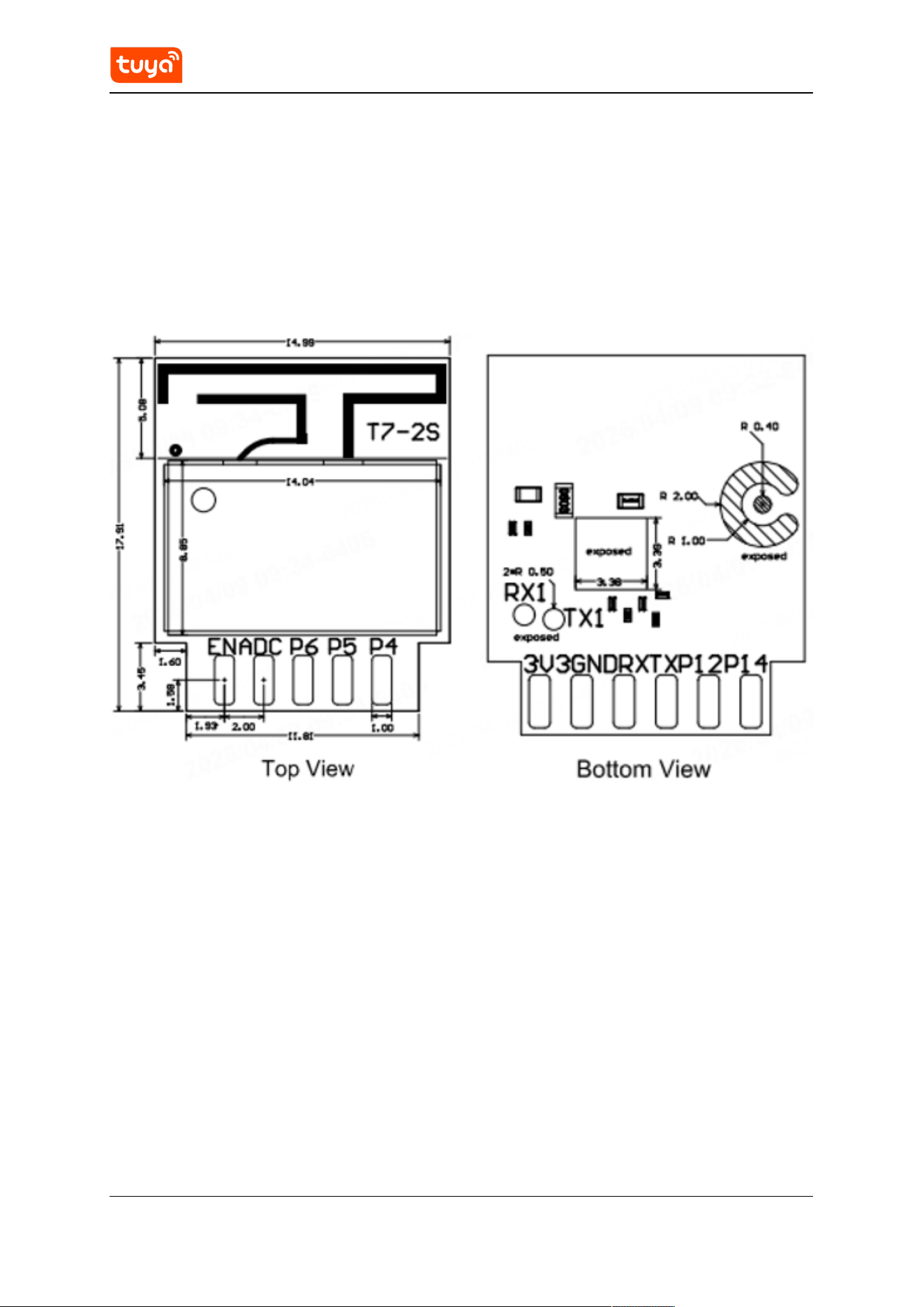
6.1. Mechanical dimensions
Mechanical dimensions of the T7-2S PCB are 14.99±0.35 mm (W) × 17.91±0.35
mm (L) × 2.8±0.15 mm (H).
The gure below shows the mechanical dimensions of T7-2S.
21 / 33
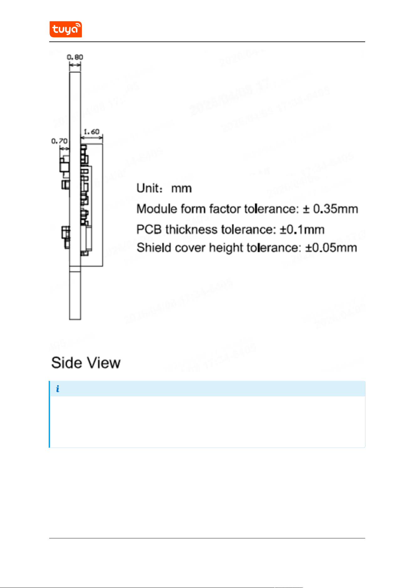
7.2MOQ and packaging information
The default tolerance of the dimensions is ±0.35 mm. If you have special
requirements for key dimensions, specify them in the datasheet after
consultations.
6.2. Recommended PCB footprint
Pin conguration of the T7-2S module:
22 / 33
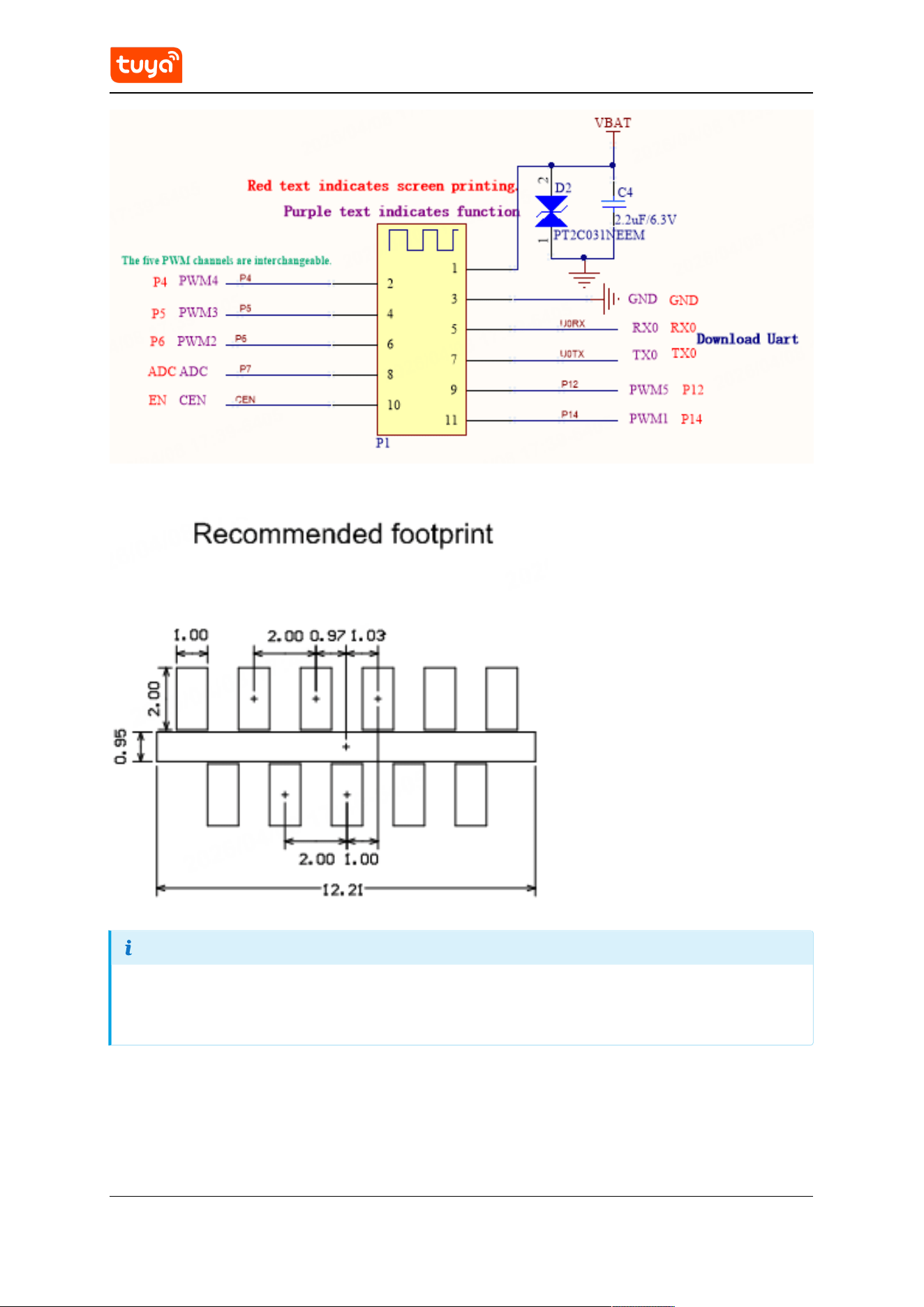
7.3MOQ and packaging information
PCB footprint of the T7-2S module:
The area indicated as keep-out in the diagram above does not require
tinning and should not have any traces routed through it.
6.3. Production instructions
• For the modules that can be packaged with the surface-mount technology
(SMT) or in in-line form, you can select either of them according to the PCB
23 / 33

7.4MOQ and packaging information
design solutions of customers. If a PCB is designed to be SMT-packaged,
package the module with the SMT. If a PCB is designed to use an in-line
package, use wave soldering. Complete soldering within 24 hours after the
module is unpacked. Otherwise, we recommend that you place the module in a
drying cupboard with a relative humidity level below 10%, or pack the module
in vacuum again. Then, record the packing time and duration of exposure. The
total exposure time cannot exceed 168 hours.
• Instruments or devices required for the SMT process:
• Surface mount system
• Solder paste inspection (SPI)
• Reow soldering machine
• Thermal proler
• Automated optical inspection (AOI) device
• Instruments or devices required for the wave soldering process:
• Wave soldering device
• Wave soldering xture
• Constant-temperature soldering iron
• Tin bar, tin wire, and ux
• Thermal proler
• Instruments or devices required for the baking process:
• Cabinet oven
• Electrostatic discharge (ESD) protection and heat-resistant trays
• ESD protection and heat-resistant gloves
• A delivered module must meet the following storage requirements:
• The moisture-proof bag must be placed in an environment where the
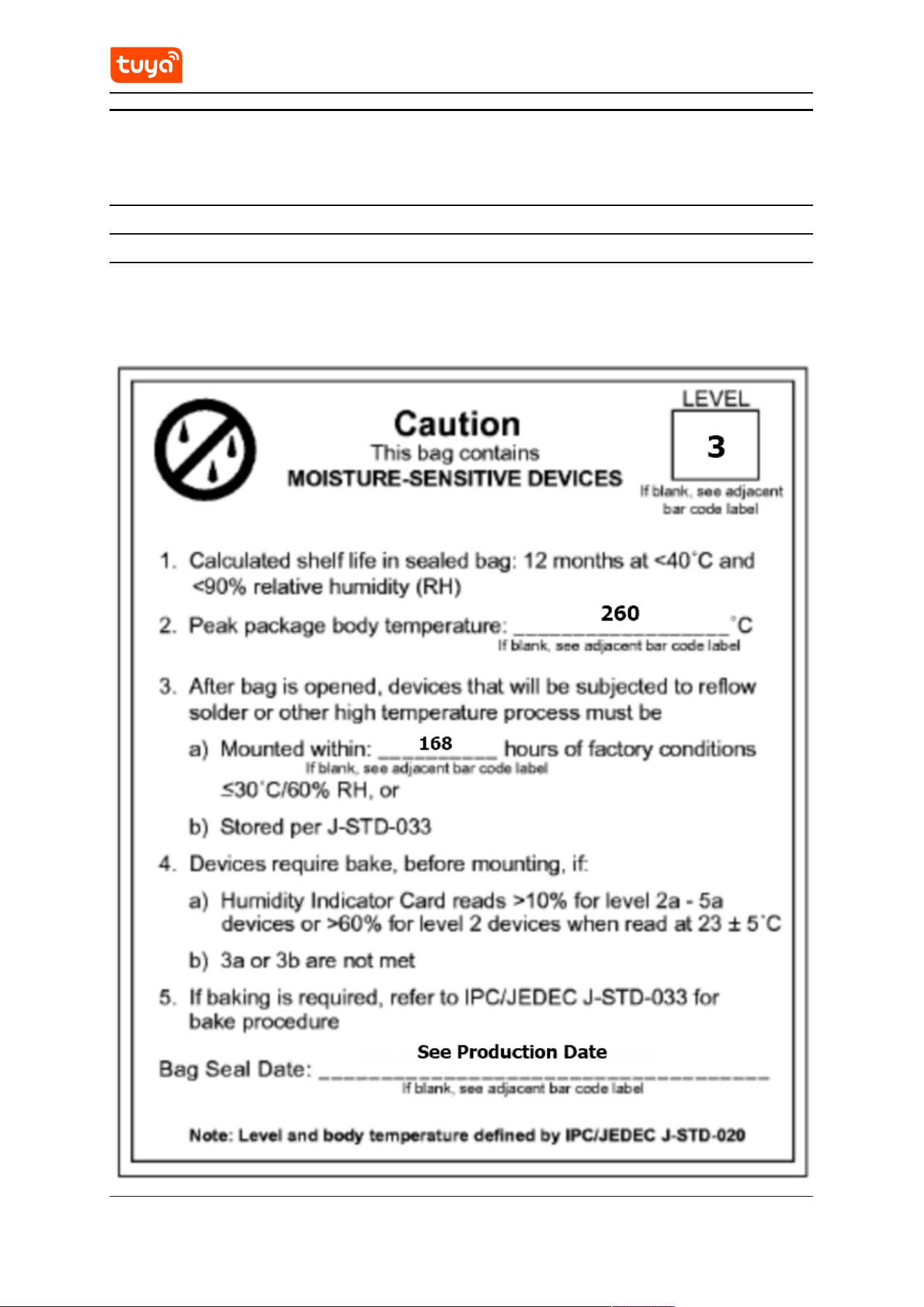
temperature is below 40°C and the relative humidity is lower than 90%.
• The shelf life of a dry-packaged product is 12 months from the date when the
product is packaged and sealed.
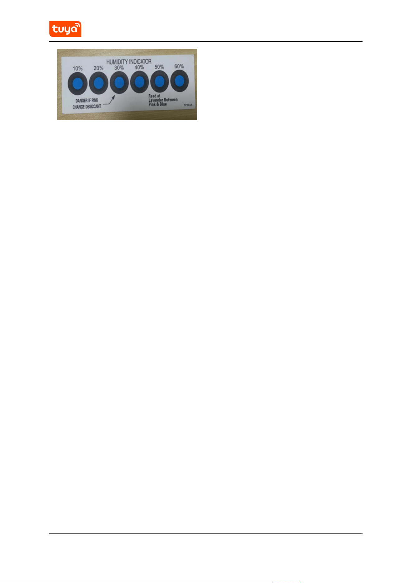
• A humidity indication card (HIC) is put in the sealed package.
24 / 33
7.4MOQ and packaging information
• The module needs to be baked in the following cases:
• The vacuum packaging bag is damaged before unpacking.
• After unpacking, no HIC is found in the packaging bag.
• After unpacking, the HIC indicates a humidity level of 10% or higher. In this
case, the circle turns pink on the HIC.
• The total exposure time has lasted for over 168 hours since unpacking.
• More than 12 months have passed since the rst sealing of the bag.
• The baking parameter settings are described below:
• Baking temperature: 40°C for reel packaging with relative humidity ≤ 5%. And
125°C for tray packaging with relative humidity ≤ 5% (use a heat-resistant
tray, rather than a plastic container).
• Baking time: 168 hours for reel packaging and 12 hours for tray packaging.
• Temperature for triggering an alert: 50°C for reel packaging and 135°C for tray
packaging.
• Production can begin after a module has cooled down to below 36°C under
natural conditions.
• If a module remains unused for over 168 hours after being baked, it needs to
be baked again.
• If a batch of modules is not baked after exposure for more than 168 hours, do
not use wave soldering to solder them. Because these modules are level-3
moisture-sensitive devices, they are very likely to get damp when exposed
beyond the allowable time. In this case, if they are soldered at high
temperatures, device failure or poor soldering performance might occur.
• In the whole production process, take electrostatic discharge (ESD) protective
measures.
• To guarantee the pass rate, we recommend that you use the SPI and AOI to
monitor the quality of solder paste printing and mounting.
25 / 33
7.4MOQ and packaging information
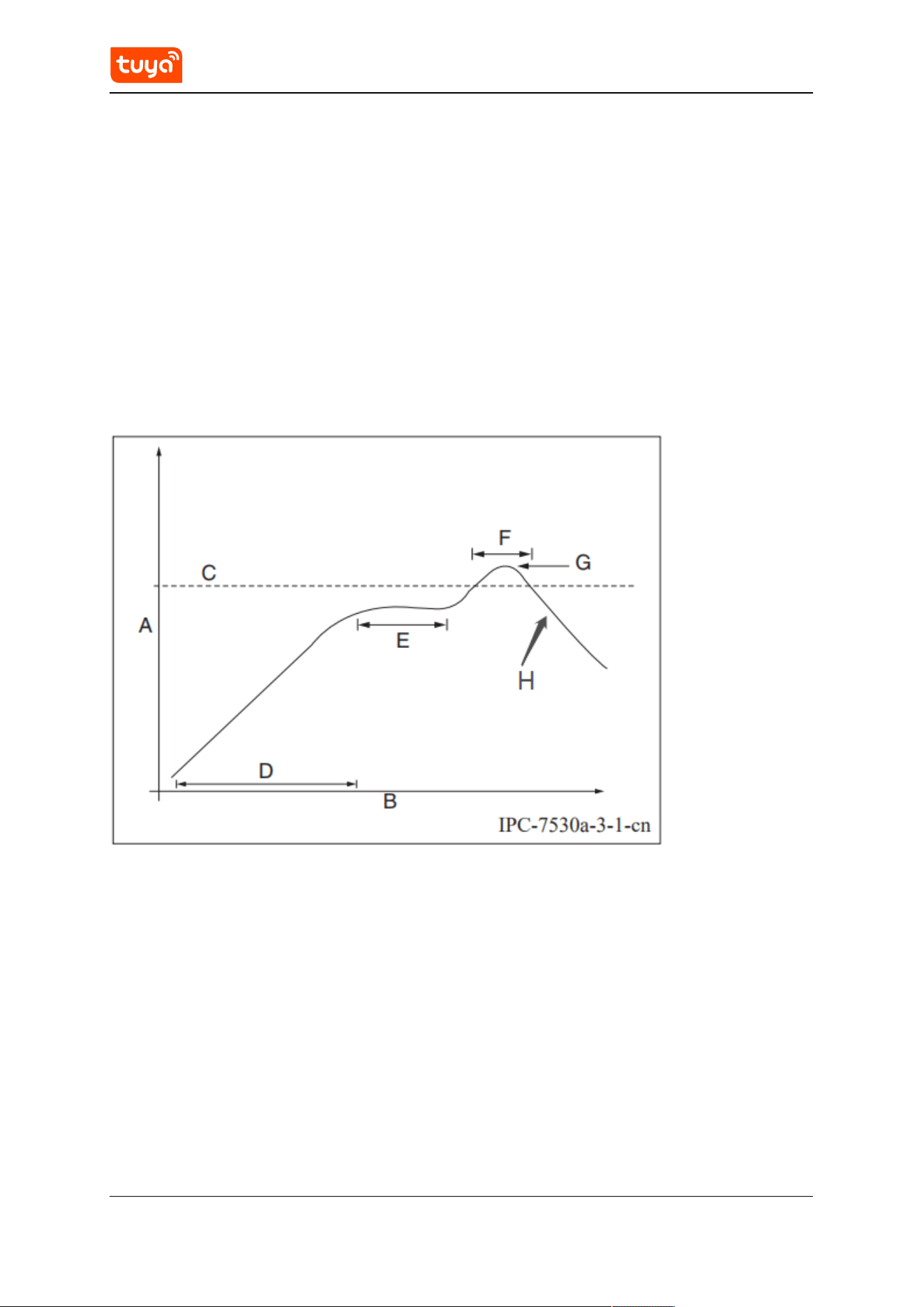
6.4. Recommended oven temperature curve
Select a proper soldering technique according to the process. For more
information, refer to the recommended oven temperature curve of either reow
soldering or wave soldering. The set temperatures might deviate from the actual
temperature measurements. All temperatures shown in this module datasheet
are obtained through actual measurements.
Technique 1: SMT process (recommended oven temperature curve of
reow soldering)
Set the oven temperatures according to the following curve.
• A: temperature axis
• B: time axis
• C: alloy liquidus temperature from 217°C to 220°C
• D: ramp-up slope from 1°C/s to 3°C/s
• E: keep a constant temperature from 150°C to 200°C for a time period of 60s to
120s
• F: temperature above liquidus temperature for 50s to 70s
• G: peak temperature from 235°C to 245°C
• H: ramp-down slope from 1°C/s to 4°C/s
26 / 33
7.5MOQ and packaging information
The curve above is based on solder paste SAC305. For more information
about other solder pastes, see the recommended oven temperature curve
in the specied solder paste specications.
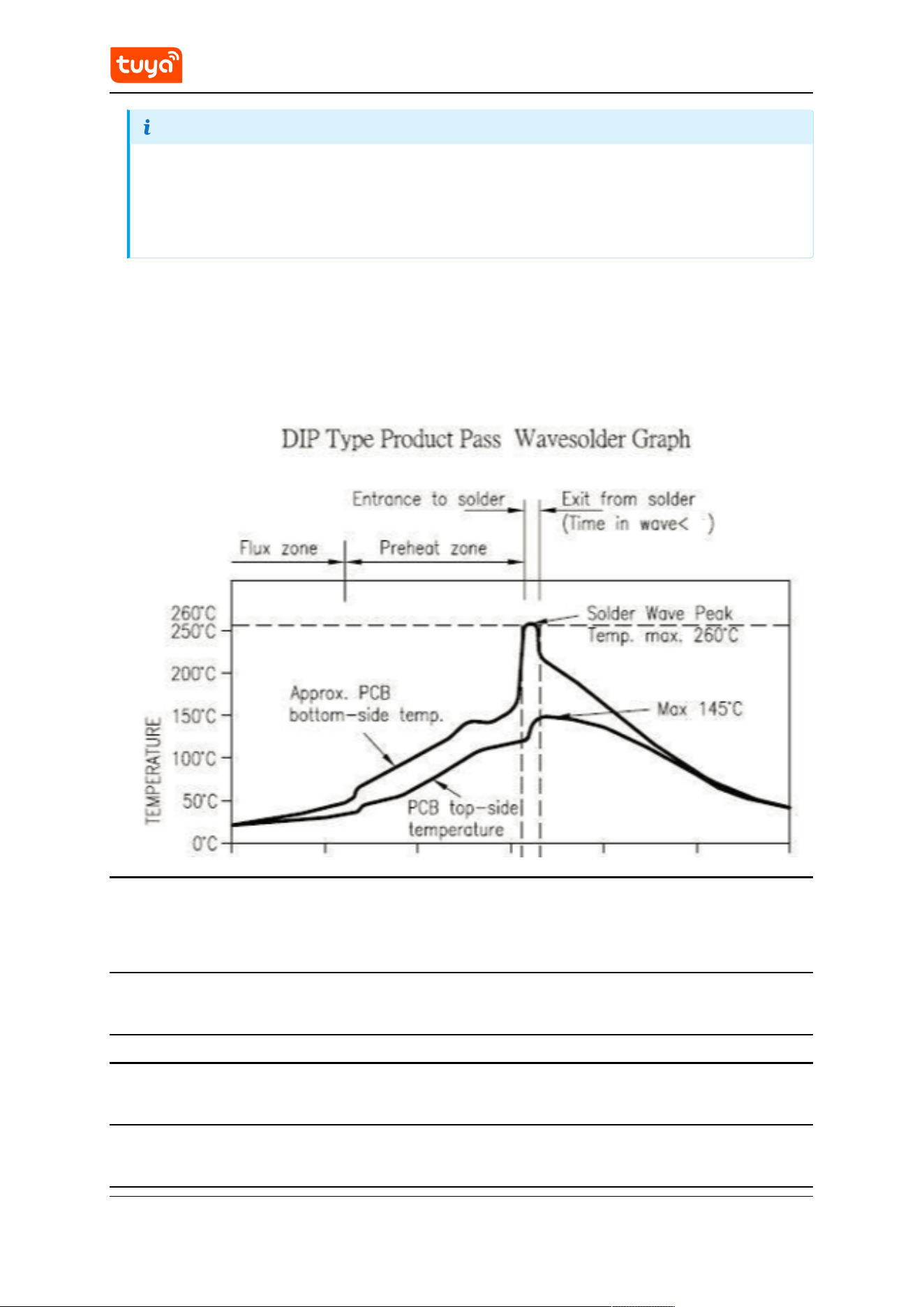
Technique 2: Wave soldering process (oven temperature curve of wave
soldering)
Set the oven temperatures according to the following temperature curve of wave
soldering. The peak temperature is 260°C±5°C.
Suggestions on
wave soldering
Suggestions on
manual repair
soldering
Preheat
temperature
80°C to 130°C
Soldering
temperature
360°C ± 20°C
Preheat duration 75s to 100s Soldering duration Less than 3s/point
Contact duration
at the peak
3s to 5s N/A N/A
Solder tank
temperature
260°C ± 5°C N/A N/A
27 / 33
7.5MOQ and packaging information
Suggestions on
wave soldering
Suggestions on
manual repair
soldering
Ramp-up slope ≤ 2°C/s N/A N/A
Ramp-down slope ≤ 6°C/s N/A N/A
6.5. Storage conditions
28 / 33

7.6MOQ and packaging information
7. MOQ and packaging information
Product
model
MOQ (pcs)
Shipping
packaging
Modules per
reel
Reels per
carton
T7-2S 4,400 Tape and reel 1,100 4
29 / 33

8Appendix: Statement
8. Appendix: Statement
Important Notice to OEM integrators
1. This module is limited to OEM installation ONLY.
2. This module is limited to installation in mobile or xed applications, according
to Part 2.1091(b).
3. The separate approval is required for all other operating congurations,
including portable congurations with respect to Part 2.1093 and dierent
antenna congurations.
4.
For FCC Part 15.31 (h) and (k): The host manufacturer is responsible for
additional testing to verify compliance as a composite system. When testing
the host device for compliance with Part15 Subpart B, the host manufacturer is
required to show compliance with Part 15 Subpart B while the transmitter
module(s) are installed and operating. The modules should be transmitting
and the evaluation should conrm that the module’s intentional emissions are
compliant (i.e. fundamental and out of band emissions). The host
manufacturer must verify that there are no additional unintentional emissions
other than what is permitted in Part 15 Subpart B or emissions are compliant
with the transmitter(s) rule(s).The Grantee will provide guidance to the host
manufacturer for Part 15 B requirements if needed.
Important Note
Notice that any deviation(s)from the dened parameters of the antenna trace, as
described by the instructions, require that the host product manufacturer must
notify Tuya that they wish to change the antenna trace design. In this case, a
Class II permissive change application is required to be led by the TUYA, or the
host manufacturer can take responsibility through the change in FCC ID (new
application) procedure followed by a Class II permissive change application.
End Product Labeling When the module is installed in the host device, the FCC
label must be visible through a window on the nal device or it must be visible
when an access panel, door, or cover is easily removed. If not, a second label
must be placed on the outside of the nal device that contains the following text:
“Contains FCC ID: 2ANDL-T72S”.The FCC ID can be used only when all FCC
compliance requirements are met.
30 / 33

Antenna Installation (1) The antenna must be installed such that 20 cm is
maintained between the antenna and users, (2) The transmitter module may not
be co-located with any other transmitter or antenna. (3) Only antennas of the
same type and with equal or less gains as shown below may be used with this
module. Other types of antennas and/or higher gain antennas may require
additional authorization for operation.
Antenna
type
BT/Wlan
2.4G
UNII-1 UNII-2 UNII-2C UNII-3
PCB 1.91dBi −1.64dBi −0.55dBi 0.8dBi 1.53dBi
In the event that these conditions cannot be met (for example, certain laptop
congurations or co-location with another transmitter), then the FCC
authorization is no longer considered valid, and the FCC ID cannot be used on the
nal product. In these circumstances, the OEM integrator will be responsible for
re-evaluating the end product (including the transmitter) and obtaining a
separate FCC authorization.
Manual Information to the End User The OEM integrator has to be aware not
to provide information to the end user regarding how to install or remove this RF
module in the user’s manual of the end product which integrates this module.
The end user manual shall include all required regulatory information/warnings as
shown in this manual.
Federal Communication Commission Interference Statement This device
complies with Part 15 of the FCC Rules. Operation is subject to the following two
conditions: (1) This device may not cause harmful interference, and (2) this
device must accept any interference received, including interference that may
cause undesired operation. This equipment has been tested and found to comply
with the limits for a Class B digital device, pursuant to Part 15 of the FCC Rules.
These limits are designed to provide reasonable protection against harmful
interference in a residential installation. This equipment generates, uses, and can
radiate radio frequency energy and, if not installed and used in accordance with
the instructions, may cause harmful interference to radio communications.
However, there is no guarantee that interference will not occur in a particular
installation. If this equipment does cause harmful interference to radio or
31 / 33

television reception, which can be determined by turning the equipment o and
on, the user is encouraged to try to correct the interference by one of the
following measures:
• Reorient or relocate the receiving antenna.
• Increase the separation between the equipment and receiver.
• Connect the equipment into an outlet on a circuit dierent from that to which
the receiver is connected.
• Consult the dealer or an experienced radio/TV technician for help.
Any changes or modications not expressly approved by the party responsible for
compliance could void the user’s authority to operate this equipment. This
transmitter must not be co-located or operating in conjunction with any other
antenna or transmitter.
List of applicable FCC rules This module has been tested and found to comply
with Part 15 requirements for Modular Approval. The modular transmitter is only
FCC authorized for the specic rule parts (i.e., FCC transmitter rules) listed on the
grant, and that the host product manufacturer is responsible for compliance with
any other FCC rules that apply to the host not covered by the modular
transmitter grant of certication. If the grantee markets their product as being
Part 15 Subpart B compliant (when it also contains unintentional-radiator digital
circuitry), then the grantee shall provide a notice stating that the nal host
product still requires Part 15 Subpart B compliance testing with the modular
transmitter installed.
This device is intended only for OEM integrators under the following conditions:
(For module device use)
1. The antenna must be installed such that 20 cm is maintained between the
antenna and users, and
2. The transmitter module may not be co-located with any other transmitter or
antenna.
As long as 2 conditions above are met, further transmitter tests will not be
required. However, the OEM integrator is still responsible for testing their end-
product for any additional compliance requirements required with this module
installed.
32 / 33

Radiation Exposure Statement This equipment complies with FCC radiation
exposure limits set forth for an uncontrolled environment. This equipment should
be installed and operated with a minimum distance of 20 cm between the
radiator & your body.
33 / 33