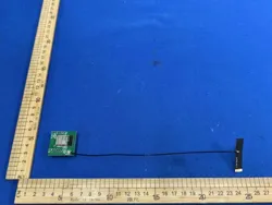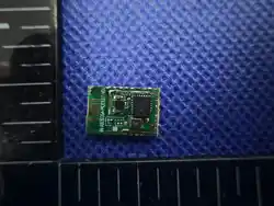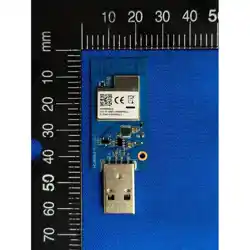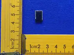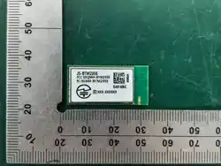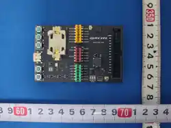

HSM110XC
Hardware Design
Short-Range Products
Version: 1.0.0
Date: 2026-04-10
Status: Preliminary

Sho
rt-Range Products
HSM110XC_Hardware_Design
1 / 53
At Quectel, our aim is to provide timely and comprehensive services to our customers. If you require any
assistance, please contact our headquarters:
Quectel Wireless Solutions Co., Ltd.
No. 8 Waipojing Road, Sijing Town, Songjiang District, Shanghai 201601, China
Tel: +86 21 5108 6236
Email: i[email protected]
Or our local offices. For more information, please visit:
https://www.quectel.com/contact/.
For technical support, or to report documentation errors, please visit:
https://www.quectel.com/tech-support/.
Or email us at: [email protected].
Legal Notices
We provide this document to support your product design. You are required to design your products based on the
specifications and parameters set forth herein. You agree that you are responsible for using independent analysis
and evaluation in designing intended products, and we provide reference designs for illustrative purposes only.
Before using any hardware, software or service guided by this document, please read this notice carefully. Even
though we employ commercially reasonable efforts to provide the best possible experience, you hereby
acknowledge and agree that this document and related services hereunder are provided to you on an “as available”
basis. You acknowledge and agree that we may add to, amend, or restate this document at any time at our sole
discretion without any prior notice to you, and such additions, amendments, or restatements shall be binding upon
you.
Use and Disclosure Restrictions
License Agreements
The recipient of any hardware, software, materials, or documentation provided by us shall keep such content
confidential, unless expressly authorized by us. The recipient shall not disclose, access, or use any part of the
received content for any purpose other than the execution and implementation of the intended project.
Copyright
Our and third-party products hereunder may contain copyrighted materials, including but not limited to protected
content, hardware, software, and documentation owned by us or applicable third parties. Unless prior written
consent is obtained, you shall not access, use, or disclose any documents or information provided by us, nor shall
you copy, reproduce, republish, display, translate, distribute, merge, modify, or create derivative works from any
such copyrighted materials. We and the applicable third party retain exclusive rights to all copyrighted materials.
No license to any patents, copyrights, trademarks, or service marks shall be granted or transferred. For the
avoidance of doubt, no form of purchase shall be construed as granting any license beyond a normal, non-exclusive,
royalty-free license to use the product. We reserve the right to pursue legal action against any violation of
confidentiality obligations, unauthorized use, or any other unlawful or malicious use of the aforementioned
documents and information.

Sho
rt-Range Products
HSM110XC_Hardware_Design
2 / 53
Trademarks
Unless otherwise expressly provided, nothing in this document shall be construed as conferring any rights to use
any trademark, trade name, name, abbreviation, or counterfeit thereof owned by us or any third party in advertising,
publicity, or any other contexts.
Third-Party Rights
You understand that this document may refer to hardware, software, and/or documentation owned by one or more
third parties (“third-party materials”). Use of such third-party materials is subject to all applicable restrictions and
obligations set forth herein.
We make no warranty or representation, either express or implied, regarding the third-party materials, including but
not limited to any implied or statutory, warranties of merchantability or fitness for a particular purpose, quiet
enjoyment, system integration, information accuracy, and non-infringement of any third-party intellectual property
rights with regard to the licensed technology or use thereof. Nothing herein constitutes a representation or warranty
by us to either develop, enhance, modify, distribute, market, sell, offer for sale, or otherwise maintain production of
any our products or any other hardware, software, device, tool, information, or product. We moreover disclaim any
and all warranties arising from the course of dealing, course of performance, or usage of trade.
Privacy Policy
To enable product functionality, certain device data may be uploaded to our or third-party servers, including those
operated by carriers, chipset suppliers, or servers designated by you. We strictly comply with applicable laws and
regulations and will retain, use, disclose, or otherwise process relevant data solely for the purpose of enabling
product functionality, or as permitted by applicable laws. Before interacting with any third party regarding data
exchange, please be informed of and understand their privacy and data security policies.
Disclaimer
a) We shall not be liable for any damages resulting from failure to comply with applicable operational or design
specifications.
b) We shall bear no liability for any inaccuracies or omissions in this document, nor for any damages arising
from the use of the information contained herein.
c) While we make every effort to ensure the integrity, accuracy, and timeliness of the features and functions
under development, errors or omissions may nevertheless occur. Unless otherwise provided in a valid written
agreement, we make no warranties of any kind, express, implied, or statutory, and disclaim all liability for
any loss or damage arising from the use of any features or functions under development, to the maximum
extent permitted by law, regardless of whether such loss or damage is foreseeable.
d) We assume no legal responsibility for the accessibility, safety, accuracy, availability, legality, or
completeness of any information, content, advertising, commercial offers, products, services, or materials on
third-party websites or third-party resources.
Copyright © Quectel Wireless Solutions Co., Ltd. 2026. All rights reserved.

Sho
rt-Range Products
HSM110XC_Hardware_Design
3 / 53
Safety Information
The following safety precautions must be observed during all phases of operation, such as usage, service or repair
of any terminal or mobile incorporating the module. Manufacturers of the terminal should notify users and
operating personnel of the following safety information by incorporating these guidelines into all manuals of the
product. Otherwise, Quectel assumes no liability for customers’ failure to comply with these precautions.
Full attention must be paid to driving at all times in order to reduce the risk of an accident.
Using a mobile while driving (even with a handsfree kit) causes distraction and can lead to
an accident.
Switch off the terminal or mobile before boarding an aircraft. The operation of wireless
appliances in an aircraft is forbidden to prevent interference with communication systems.
If there is an Airplane Mode, it should be enabled prior to boarding an aircraft. Please
consult the airline staff for more restrictions on the use of wireless devices on an aircraft.
Wireless devices may cause interference on sensitive medical equipment, so please be
aware of the restrictions on the use of wireless devices when in hospitals, clinics or other
healthcare facilities.
The terminal or mobile contains a transceiver. When it is ON, it receives and transmits
radio frequency signals. RF interference can occur if it is used close to TV sets, radios,
computers or other electric equipment.
In locations with explosive or potentially explosive atmospheres, obey all posted signs and
turn off wireless devices such as mobile phone or other terminals. Areas with explosive or
potentially explosive atmospheres include fueling areas, below decks on boats, fuel or
chemical transfer or storage facilities, and areas where the air contains chemicals or
particles such as grain, dust or metal powders.

Sho
rt-Range Products
HSM110XC_Hardware_Design
4 / 53
About the Document
Revision History
Version Date Author Description
- 2026-04-07
Jason Zhao/
Stephen Li
Creation of the document
1.0.0 2026-04-10
Jason Zhao/
Stephen Li
Preliminary

Sho
rt-Range Products
HSM110XC_Hardware_Design
5 / 53
Contents
Safety Information ...................................................................................................................................................... 3
About the Document ................................................................................................................................................... 4
Contents ....................................................................................................................................................................... 5
Table Index .................................................................................................................................................................. 7
Figure Index ................................................................................................................................................................ 8
1 Introduction ............................................................................................................................................................ 9
2 Product Overview ................................................................................................................................................... 9
2.1. Key Features ................................................................................................................................................ 10
3 Application Interfaces .......................................................................................................................................... 12
3.1. Pin Assignment ............................................................................................................................................ 12
3.2. Pin Definitions ............................................................................................................................................. 13
3.3. GPIO Multiplexing ...................................................................................................................................... 16
3.4. Application Interfaces .................................................................................................................................. 19
3.4.1. UART Interface ................................................................................................................................ 19
3.4.2. SPI Interface ..................................................................................................................................... 20
3.4.3. I2C Interface ..................................................................................................................................... 21
3.4.4. ADC Interfaces ................................................................................................................................. 21
4 Operating Characteristics .................................................................................................................................... 23
4.1. Power Supply ............................................................................................................................................... 23
4.1.1. Reference Design for Power Supply ................................................................................................. 23
4.2. Reset ............................................................................................................................................................ 24
4.3. Download Mode .......................................................................................................................................... 25
5 RF Specifications .................................................................................................................................................. 26
5.1. Bluetooth Performances ............................................................................................................................... 26
5.2. Antenna Interfaces ..................................................................................................................................... 26
5.2.1. Antenna Interfaces ............................................................................................................................ 27
5.2.2. Reference Design of ANT_EX ......................................................................................................... 27
5.2.3. RF Routing Guidelines ..................................................................................................................... 28
5.2.4. RF Connector Recommendation ....................................................................................................... 29
5.2.4.1. Antenna Connector Specifications ......................................................................................... 29
5.2.4.2. Antenna Connector Installation ............................................................................................. 30
5.2.4.3. Recommended Manufacturers of RF Connector and Cable................................................... 32
5.2.5. Requirements for Antenna Design .................................................................................................... 32
5.2.6. Antenna Direction Diagram .............................................................................................................. 32
6 Electrical Characteristics and Reliability ........................................................................................................... 34
6.1. Absolute Maximum Ratings ........................................................................................................................ 34

Sho
rt-Range Products
HSM110XC_Hardware_Design
6 / 53
6.2. Power Supply Ratings .................................................................................................................................. 34
6.3. Bluetooth Power Consumption .................................................................................................................... 35
6.4. Digital I/O Characteristics ........................................................................................................................... 36
6.5. ESD Protection ............................................................................................................................................ 36
7 Mechanical Information ....................................................................................................................................... 37
7.1. Mechanical Dimensions ............................................................................................................................... 37
7.2. Recommended Footprint .............................................................................................................................. 38
7.3. Top View ..................................................................................................................................................... 39
8 Storage, Manufacturing and Packaging ............................................................................................................. 40
8.1. Storage Conditions ....................................................................................................................................... 40
8.2. Manufacturing and Soldering ...................................................................................................................... 40
8.3. Packaging Specifications ............................................................................................................................. 42
8.3.1. Carrier Tape ...................................................................................................................................... 42
8.3.2. Plastic Reel ....................................................................................................................................... 43
8.3.3. Mounting Direction ........................................................................................................................... 43
8.3.4. Packaging Process............................................................................................................................. 44
9 Appendix References ............................................................................................................................................ 45

Sho
rt-Range Products
HSM110XC_Hardware_Design
7 / 53
Table Index
Table 1: Basic Information .......................................................................................................................................... 9
Table 2: Key Features ................................................................................................................................................ 10
Table 3: Parameter Definition ................................................................................................................................... 13
Table 4: Pin Description ............................................................................................................................................ 13
Table 5: GPIO Multiplexing ...................................................................................................................................... 16
Table 6: Pin Description of UART Interface ............................................................................................................. 19
Table 7: Pin Description of SPI ................................................................................................................................. 20
Table 8: Pin Description of I2C Interface .................................................................................................................. 21
Table 9: Pin Description of ADC Interfaces .............................................................................................................. 21
Table 10: ADC Features ............................................................................................................................................ 22
Table 11: Pin Description of Power Supply and GND Pins ...................................................................................... 23
Table 12: Pin Description of RESET_N .................................................................................................................... 24
Table 13: Bluetooth Performances ............................................................................................................................ 26
Table 14: Pin Description of ANT_IN and ANT_EX ............................................................................................... 27
Table 15: Major Specifications of the RF Connector ................................................................................................ 30
Table 16: Requirements for Antenna Design............................................................................................................. 32
Table 17: Absolute Maximum Ratings (Unit: V) ...................................................................................................... 34
Table 18: Module’s Power Supply Ratings (Unit: V) ............................................................................................... 34
Table 19: Bluetooth Power Consumption (Unit: mA; Max.)..................................................................................... 35
Table 20: Power Consumption in Sleep Mode (Unit: μA; Typ.) ............................................................................... 35
Table 21: VBAT I/O Characteristics (Unit: V) .......................................................................................................... 36
Table 22: Electrostatic Discharge Characteristics (Unit: kV) .................................................................................... 36
Table 23: Recommended Thermal Profile Parameters .............................................................................................. 41
Table 24: Carrier Tape Dimension Table (Unit: mm) ............................................................................................... 42
Table 25: Plastic Reel Dimension Table (Unit: mm) ................................................................................................. 43
Table 26: Related Documents .................................................................................................................................... 45
Table 27: Terms and Abbreviations ........................................................................................................................... 45

Sho
rt-Range Products
HSM110XC_Hardware_Design
8 / 53
Figure Index
Figure 2 : Pin Assignment (Top View) ....................................................................................................................... 12
Figure 3 : UART1 Interface Connection Diagram ..................................................................................................... 19
Figure 4 : SPI Interface Connection Diagram (Master Mode) .................................................................................... 21
Figure 5 : Reference Design of Power Supply ............................................................................................................ 24
Figure 6 : Reference Circuit of Reset with Driving Circuit ........................................................................................ 24
Figure 7 : Reference Circuit of Reset with a Button ................................................................................................... 25
Figure 8 : Reset Timing .............................................................................................................................................. 25
Figure 9 : Reference Design of Antenna Interface (ANT_EX) .................................................................................. 27
Figure 10 : Microstrip Design on a 2-layer PCB ........................................................................................................ 28
Figure 11 : Coplanar Waveguide Design on a 2-layer PCB ....................................................................................... 28
Figure 12 : Coplanar Waveguide Design on a 4-layer PCB (Layer 3 as Reference Ground) ..................................... 29
Figure 13 : Coplanar Waveguide Design on a 4-layer PCB (Layer 4 as Reference Ground) ..................................... 29
Figure 14 : Dimensions of the Receptacle (Unit: mm) ............................................................................................... 30
Figure 15 : Dimensions of the Receptacle (Unit: mm) ............................................................................................... 31
Figure 16 : Space Factor of Mated Connectors (Ø 0.81 mm Coaxial Cables) (Unit: mm) ......................................... 31
Figure 17 : Space Factor of Mated Connectors (Ø 1.13 mm Coaxial Cables) (Unit: mm) ......................................... 32
Figure 18 : Antenna Direction Diagram ..................................................................................................................... 33
Figure 19 : Top and Side Dimensions ........................................................................................................................ 37
Figure 20 : Recommended Footprint .......................................................................................................................... 38
Figure 21 : Top View .................................................................................................................................................. 39
Figure 22 : Recommended Reflow Soldering Thermal Profile .................................................................................. 41
Figure 23 : Carrier Tape Dimension Drawing (Unit: mm) ......................................................................................... 42
Figure 24 : Plastic Reel Dimension Drawing ............................................................................................................. 43
Figure 25 : Mounting Direction .................................................................................................................................. 43
Figure 26 : Packaging Process .................................................................................................................................... 44

Sho
rt-Range Products
HSM110XC_Hardware_Design
9 / 53
1 Introduction
This document defines HSM110XC in Open solution and describes its hardware interfaces and air interfaces
connected to your applications, which can help you quickly understand the hardware interface characteristics, RF
characteristics, electrical characteristics, mechanical specifications and other relevant information of the module.
The module has no RF shielding
The Class Il permissive changes is required for each specific host installation
2 Product Overview
HSM110XC is a low-power, cost-effective Bluetooth module supporting BLE 5.4 protocol. It features built-in
power management unit. The module has ultra-low power consumption, with broadcast power consumption as low
as 10 μA, and connected power consumption as low as 7 μA (both at 1‑second intervals). The module has multiple
interfaces such as UART, SPI, I2C and ADC for various applications.
The module is an SMD module with compact packaging. The general features of the module are as follow:
ARM Cortex-M4 processor with 64 MHz low-power
EFUSE: 256-bit
80 KB SRAM memory, 1 MB Flash, and 8 KB I-Cache (command cache)
Ultra-low power consumption
Table 1: Basic Information
HSM110XC
Product Form SIP
Packaging Type LGA
Pin Counts 33
Dimensions
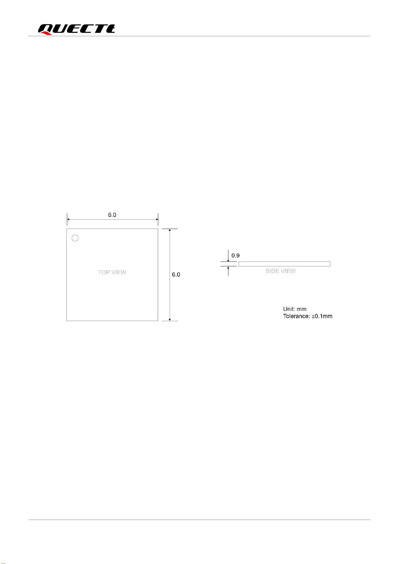
(6 ±0.1) mm × (6 ±0.1) mm × (0.9 ±0.1) mm

Sho
rt-Range Products
HSM110XC_Hardware_Design
10 / 53
2.1. Key Features
Table 2: Key Features
1
Within this range, the module’s indicators comply with Bluetooth specification requirements.
2
Quectel supplies a HSM110XC-TE-B with accessories to develop and test the module.
3
The module is provided with one of the two antenna interface designs. For more details, please contact Quectel Technical Support.
Weight Approx. 0.05 g
Basic Information
Protocol and Standard
Bluetooth protocol: BLE 5.4
All hardware components fully comply with EU RoHS directive
Supply Voltage
VBAT Power Supply:
1.71–3.6 V
Typ. 3.3 V
Temperature Ranges
Normal operating temperature
1
: -40 °C to +85 °C
Storage temperature: -45 °C to +95 °C
TE-B Kit HSM110XC-TE-B
2
RF Antenna Interfaces
3
Antenna Interfaces
ANT_IN, ANT_EX (optional)
50 Ω impedance
Application Interfaces
4
Application Interfaces UART, SPI, I2C, ADC

Sho
rt-Range Products
HSM110XC_Hardware_Design
11 / 53
Sho
rt-Range Products
HSM110XC_Hardware_Design
12 / 53
3 Application Interfaces
3.1. Pin Assignment
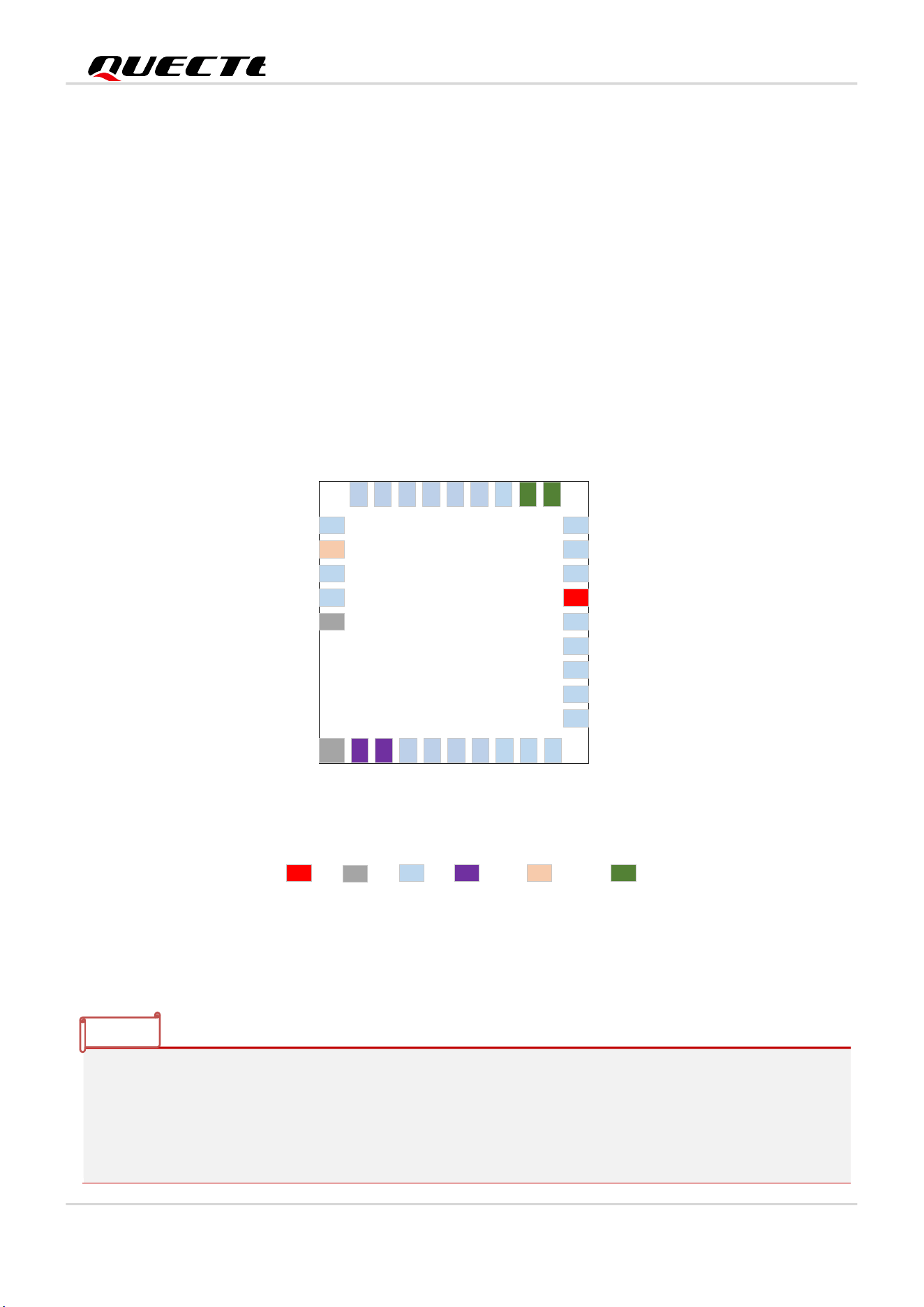
1
2
3
4
5
6
7
8
9
10
11
12
13
14
15
HSM110XC
GPIO_2
RESET_N
GPIO_25
GPIO_24
GND
GND
ANT_IN
ANT_EX
GPIO_23
GPIO_22
GPIO_21
GPIO_6
GPIO_5
GPIO_4
GPIO_1
GND
GPIO
ANT
CONTROL RESERVED
POWER
16
GPIO_0
17
GPIO_20
18
19
20
21
22
23
24
GPIO_19
GPIO_18
GPIO_10
VBAT
GPIO_9
GPIO_17
GPIO_16
33
32
31
30
29
28
27
26
25
RESERVED
GPIO_15
GPIO_14
GPIO_12
GPIO_11
GPIO_7
GPIO_8
GPIO_3
RESERVED
Figure 1: Pin Assignment (Top View)
1. Keep all RESERVED and unused pins open.
2. All GND pins should be connected to ground.
3. Ensure that there is no current sink on all module pins except input power supply pins before the module
turns on.
4. The module has 25 GPIO interfaces by default. In the case of multiplexing, it supports interfaces including
NOTE
Sho
rt-Range Products
HSM110XC_Hardware_Design
13 / 53
UART, SPI, I2C and ADC. For more details, see Chapter 3.3 and Chapter 3.4.
3.2. Pin Definitions
Table 3: Parameter Definition
DC characteristics include power domain and rated current.
Table 4: Pin Description
Parameter Description
AIO Analog Input/Output
DI Digital Input
DIO Digital Input/Output
PI Power Input
PU Pull Up
Hi-Z High Impedance
Power Supply and GND Pins
Pin Name Pin No.
I/O
Status
after
Reset
Description
DC
Characteristics
Comment
VABT 21 PI -
Power supply for
the module
Vmin = 1.71 V
Vnom = 3.3 V
Vmax = 3.6 V
It is recommended to
provide a current of at
least 0.1 A.
GND 5, 6
Connect them to the
ground.
Reset
Pin Name Pin No.
I/O
Status
after
Reset
Description
DC
Characteristics
Comment
RESET_N 2 DI Hi-Z
Reset the
module
VBAT
Hardware reset.
Active low.

Sho
rt-Range Products
HSM110XC_Hardware_Design
14 / 53
GPIO Interfaces
Pin Name Pin No.
I/O
Status
after
Reset
Description
DC
Characteristics
Comment
GPIO_2 1 DIO Hi-Z
General-purpose
input/output
VBAT
GPIO_25 3 DIO Hi-Z
General-purpose
input/output
GPIO_24 4 DIO Hi-Z
General-purpose
input/output
GPIO_23 9 DIO Hi-Z
General-purpose
input/output
GPIO_22 10 DIO Hi-Z
General-purpose
input/output
GPIO_21 11 DIO Hi-Z
General-purpose
input/output
GPIO_6 12 DIO Hi-Z
General-purpose
input/output
GPIO_5 13 DIO Hi-Z
General-purpose
input/output
GPIO_4 14 DIO Hi-Z
General-purpose
input/output
GPIO_1 15 DIO Hi-Z
General-purpose
input/output
GPIO_0 16 DIO Hi-Z
General-purpose
input/output
GPIO_20 17 DIO Hi-Z
General-purpose
input/output
GPIO_19 18 DIO Hi-Z
General-purpose
input/output
GPIO_18 19 DIO Hi-Z
General-purpose
input/output
GPIO_10 20 DIO Hi-Z
General-purpose
input/output
GPIO_9 22 DIO Hi-Z
General-purpose
input/output
GPIO_17 23 DIO Hi-Z
General-purpose
input/output
GPIO_16 24 DIO Hi-Z
General-purpose
input/output
GPIO_15 27 DIO Hi-Z
General-purpose
input/output
Sho
rt-Range Products
HSM110XC_Hardware_Design
15 / 53
To reduce the probability of module damage and extend module service life, do not power up and down
frequently.
GPIO_14 28 DIO Hi-Z
General-purpose
input/output
GPIO_12 29 DIO Hi-Z
General-purpose
input/output
GPIO_11 30 DIO Hi-Z
General-purpose
input/output
GPIO_7 31 DIO Hi-Z
General-purpose
input/output
GPIO_8 32 DIO Hi-Z
General-purpose
input/output
GPIO_3 33 DIO Hi-Z
General-purpose
input/output
RF Antenna Interfaces
Pin Name Pin No.
I/O
Status
after
Reset
Description
DC
Characteristics
Comment
ANT_IN 7 AIO -
Bluetooth
antenna interface
(module internal
antenna)
50 Ω impedance.
ANT_EX 8 AIO -
Bluetooth
antenna interface
RESERVED Pins
Pin Name Pin No. Comment
RESERVED 25, 26 Keep them open.
NOTE
Short-Range Products
HSM110XC_Hardware_Design
16 / 53
3.3. GPIO Multiplexing
The module supports 25 GPIO interfaces. THe multiplexing details are shown in the following figure:
Table 5: GPIO Multiplexing
Pin Name
Pin
No.
Alternate Function
0
(GPIO No.)
Alternate
Function 1
Alternate
Function 2
Alternate Function
3
Alternate
Function 4
Alternate
Function 5
GPIO_0 16 GPIO_0 UART0_TX - SPI0_MISO I2C_SCL -
GPIO_1 15 GPIO_1 UART0_RX UART1_CTS SPI0_MOSI I2C_SDA -
GPIO_2 1 GPIO_2 UART0_TX UART1_RTS SPI0_CSN I2C_SCL ADC1
GPIO_3 33 GPIO_3 UART0_RX UART1_RX SPI0_SCK I2C_SDA ADC2
GPIO_4 14 GPIO_4 UART0_TX UART1_TX SPI1_MISO I2C_SCL BOOT
GPIO_5 13 GPIO_5 UART0_TX UART1_TX SPI1_MOSI I2C_SDA -
GPIO_6 12 GPIO_6 UART0_RX UART1_RX SPI1_CSN I2C_SCL -
GPIO_7 31 GPIO_7 UART0_RX UART1_CTS SPI1_SCK I2C_SDA ADC3
GPIO_8 32 GPIO_8 UART0_TX UART1_RTS SPI0_MISO I2C_SCL ADC4
GPIO_9 22 GPIO_9 UART0_RX UART1_RX SPI0_MOSI I2C_SDA -

Short-Range Products
HSM110XC_Hardware_Design
17 / 53
GPIO_10 20 GPIO_10 UART0_TX UART1_TX SPI0_CSN I2C_SCL -
GPIO_11 30 GPIO_11 UART0_RX UART1_CTS SPI0_SCK I2C_SDA ADC5
GPIO_12 29 GPIO_12 UART0_TX UART1_RTS SPI1_MISO I2C_SCL ADC6
GPIO_14 28 GPIO_14 UART0_TX UART1_TX SPI1_CSN I2C_SCL ADC7
GPIO_15 27 GPIO_15 UART0_RX UART1_CTS SPI1_SCK I2C_SDA ADC8
GPIO_16 24 GPIO_16 UART0_TX UART1_RTS SPI0_MISO I2C_SCL -
GPIO_17 23 GPIO_17 UART0_RX UART1_RX SPI0_MOSI I2C_SDA -
GPIO_18 19 GPIO_18 UART0_TX UART1_TX SPI0_CSN I2C_SCL -
GPIO_19 18 GPIO_19 UART0_RX UART1_CTS SPI0_SCK I2C_SDA -
GPIO_20 17 GPIO_20 UART0_TX UART1_RTS SPI1_MISO I2C_SCL -
GPIO_21 11 GPIO_21 UART0_RX UART1_RX SPI1_MOSI I2C_SDA -
GPIO_22 10 GPIO_22 UART0_TX UART1_TX SPI1_CSN I2C_SCL -
GPIO_23 9 GPIO_23 UART0_RX - SPI1_SCK I2C_SDA -
GPIO_24 4 GPIO_24 UART0_TX UART1_RX SPI0_MISO I2C_SCL -
GPIO_25 3 GPIO_25 UART0_RX UART1_TX SPI0_MOSI I2C_SDA -
Short-Range Products
HSM110XC_Hardware_Design
18 / 53
1.After the module is powered down, all of its GPIO interfaces must be driven low. Otherwise, the current leakage may make the module enter an abnormal status.
2.The maximum number of each application interface multiplexed with GPIO interfaces is not available simultaneously. For more details, see Chapter 3.4.
NOTE
Sh
ort-Range Products
HSM110XC_Hardware_Design
19 / 53
3.4. Application Interfaces
3.4.1. UART Interface
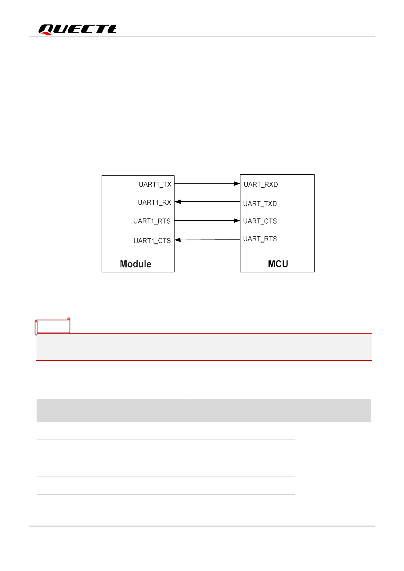
In the case of multiplexing, the module supports up to two UART interfaces. UART1 interface supports hardware
flow control, and it can be used for data transmission with peripherals. The two UART interfaces all support baud
rates up to 921600 bps.
The UART1 interface connection between the module and the MCU is shown below:
Figure 2: UART1 Interface Connection Diagram
To increase the stability of UART1 communication, it is recommended to add UART1 hardware flow control
design.
Table 6: Pin Description of UART Interface
Pin Name Pin No.
Multiplexing
Function
I/O Description Comment
GPIO_5 13 UART0_TX DO UART0 transmit
For other multiplexing
UART configuration,
see Table 5.
GPIO_6 12 UART0_RX DI UART0 receive
GPIO_4 14 UART1_TX DO UART1 transmit
GPIO_3 33 UART1_RX DI UART1 receive
GPIO_2 1 UART1_RTS DO
Request to send
signal from the
NOTE

Sh
ort-Range Products
HSM110XC_Hardware_Design
20 / 53
3.4.2. SPI Interface
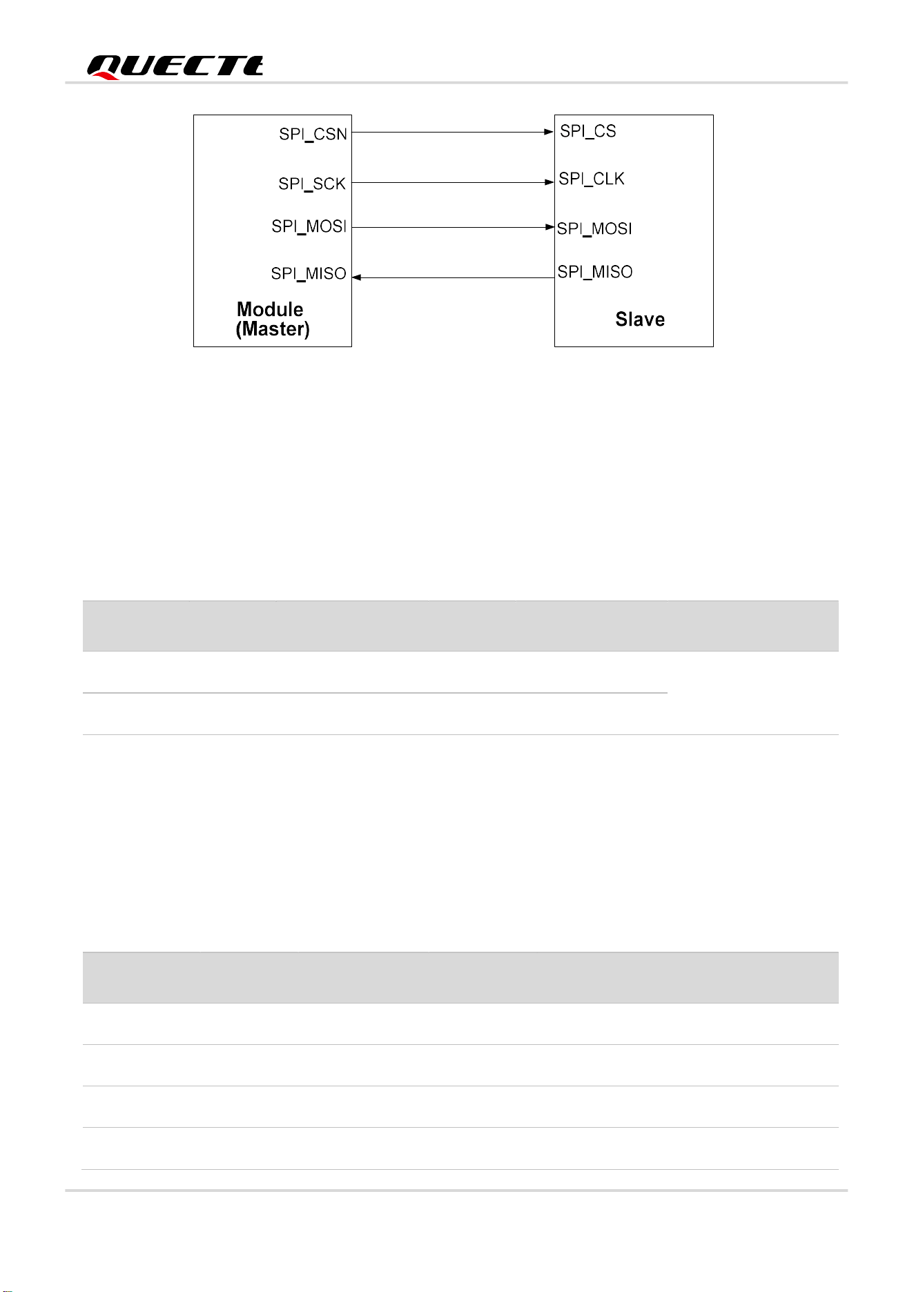
In the case of multiplexing, the module supports two SPI interfaces, which support both master and slave modes
(operating at master mode by default). The maximum clock frequency is 32 MHz. For another multiplexing SPI
configuration, see Table 5.
Table 7: Pin Description of SPI
The common connection of SPI interface is shown below.
module
GPIO_1 15 UART1_CTS DI
Clear to send signal
to the module
Pin Name Pin No.
Multiplexing
Function
I/O Description Comment
GPIO_8 32 SPI0_MISO DIO
SPI0 master-in slave-
out
GPIO_9 22 SPI0_MOSI DIO
SPI0 master-out slave-
in
GPIO_10 20 SPI0_CSN DIO SPI0 chip select
They are output signals in
master mode and input
signals in slave mode.
GPIO_11 30 SPI0_SCK DIO SPI0 clock
GPIO_20 17 SPI1_MISO DIO
SPI1 master-in slave-
out
GPIO_21 11 SPI1_MOSI DIO
SPI1 master-out slave-
in
GPIO_22 10 SPI1_CSN DIO SPI1 chip select
They are output signals in
master mode and input
signals in slave mode.
GPIO_23 09 SPI1_SCK DIO SPI1 clock
Sh
ort-Range Products
HSM110XC_Hardware_Design
21 / 53
Figure 3: SPI Interface Connection Diagram (Master Mode)
3.4.3. I2C Interface
In the case of multiplexing, the module supports up to one I2C interface.
Table 8: Pin Description of I2C Interface
3.4.4. ADC Interfaces
In the case of multiplexing, the module supports up to eight ADC interfaces. To improve the voltage measurement
accuracy, the trace of ADC interface should be surrounded by ground.
Table 9: Pin Description of ADC Interfaces
Pin Name Pin No.
Multiplexing
Function
I/O Description Comment
GPIO_14 28 I2C_SCL OD I2C serial clock
For other multiplexing
I2C configuration, see
Table 5.
GPIO_15 27 I2C_SDA OD I2C serial data
Pin Name Pin No.
Multiplexing
Function
I/O Description
GPIO_2 1 ADC1 AI General ADC1 interface
GPIO_3 33 ADC2 AI General ADC2 interface
GPIO_7 31 ADC3 AI General ADC3 interface
GPIO_8 32 ADC4 AI General ADC4 interface
Sh
ort-Range Products
HSM110XC_Hardware_Design
22 / 53
Table 10: ADC Features
1. The input voltage of every ADC interface should not exceed its corresponding voltage range.
2. It is prohibited to supply any voltage to ADC interface when the nodule is not powered by the VBAT.
3. It is recommended to use a resistor divider circuit for ADC application.
GPIO_11 30 ADC5 AI General ADC5 interface
GPIO_12 29 ADC6 AI General ADC6 interface
GPIO_14 28 ADC7 AI General ADC7 interface
GPIO_15 27 ADC8 AI General ADC8 interface
Parameter Min. Typ. Max. Unit
ADC Input Voltage 0 - VBAT V
ADC Resolution - 12 - bit
NOTE
Sh
ort-Range Products
HSM110XC_Hardware_Design
23 / 53
4 Operating Characteristics
4.1. Power Supply
Table 11: Pin Description of Power Supply and GND Pins
4.1.1. Reference Design for Power Supply
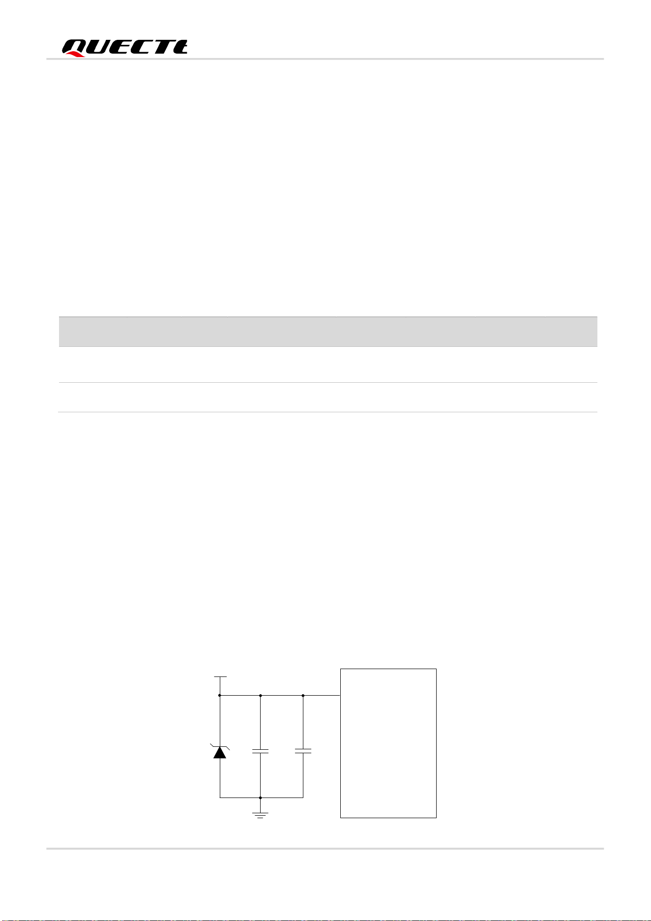
The module is powered by VBAT, and it is recommended to use a power supply chip that provides at least 0.1 A
to ensure sufficient current. For better power supply performance, it is recommended to parallel two filter
capacitors of 1 μF and 100 nF near the module’s VBAT pin. In addition, to avoid ripple and surge and ensure the
stability of the power supply to the module, add a TVS diode with adequate surge power capability on each input
power rail. If the TVS is not added, surges on the input power rail may cause damage to the module. As per design
rules, the longer the VBAT trace is, the wider it should be.
The reference design for the VBAT is shown below:
Module
VBAT
VBAT
D1
C2
C3
1 μF
100 nF
Pin Name Pin No. I/O Description Min. Typ. Max. Unit
VBAT 21 PI
Power supply for the
module
1.71 3.3 3.6 V
GND 5, 6
Sh
ort-Range Products
HSM110XC_Hardware_Design
24 / 53
Figure 4: Reference Design of Power Supply
4.2. Reset
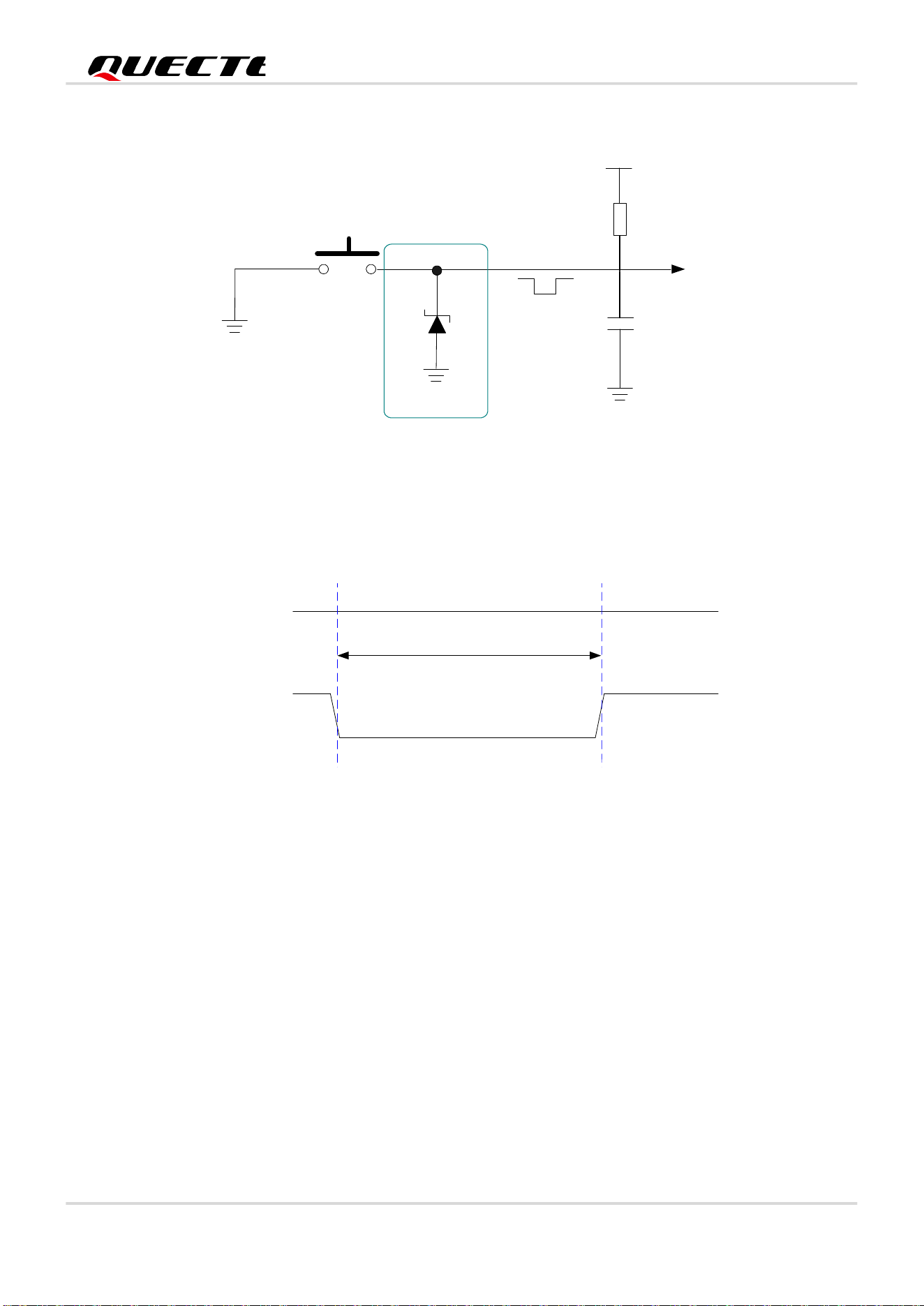
Pull RESET_N down to 0.3 V for at least 40 μs and then release it to reset the module. In order to avoid module
restart due to abnormal interference, it is recommended to route the trace as short as possible and surround it with
ground. It is also recommended to add a 10 kΩ pull-up resistor on the RESET_N signal trace to VBAT, and a 100
nF pull-down capacitor to GND in parallel.
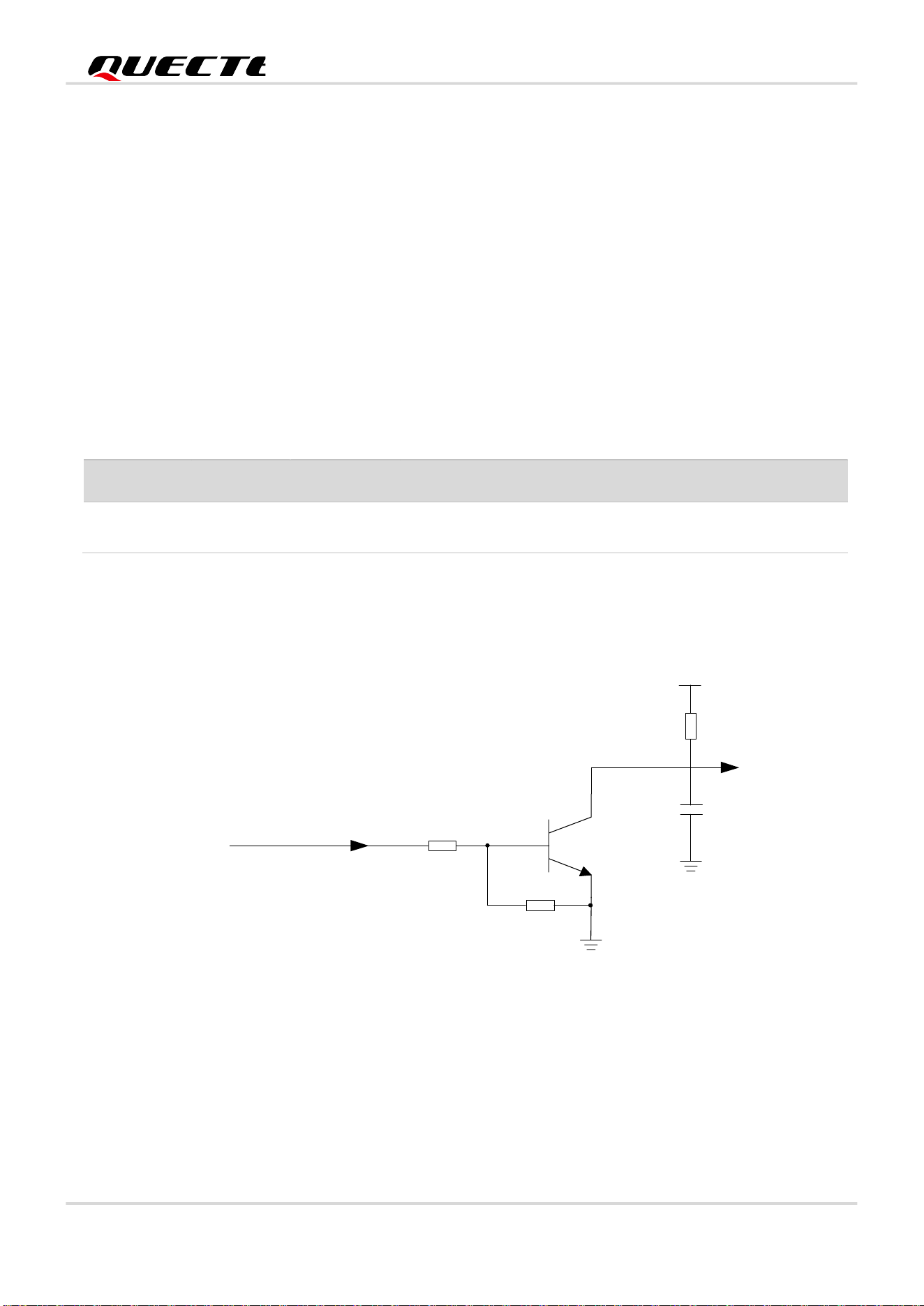
Table 12: Pin Description of RESET_N
It is recommended to use an open-collector driver circuit to control RESET_N.
RESET_N
4.7 kΩ
47 kΩ
Control
Q1
R2
R1
VBAT
10 kΩ
100nF
Figure 5: Reference Circuit of Reset with Driving Circuit
Another way to control the RESET_N pin is by using a button directly. A TVS diode should be placed near the
button for protection against ESD, since static electricity may be generated by the touch of a finger. A reference
circuit is shown in the following figure.
Pin Name Pin No. I/O Description Comment
RESET_N 2 DI Reset the module
Hardware reset.
Active low.
Sh
ort-Range Products
HSM110XC_Hardware_Design
25 / 53
RESET_N
S1
Closed to S1
TVS
VBAT
10 kΩ
100nF
Figure 6: Reference Circuit of Reset with a Button
The module reset timing is shown below:
V
IL
≤ 0.3V
V
IH
≥ 2.4V
VBAT
RESET_N
T ≥ 40 us
Figure 7: Reset Timing
4.3. Download Mode
Pull down the BOOT pin (GPIO_4) when the module is powered up, then power it down and up again to enable
the module to enter the download mode. In the download mode, UART0 can be used for firmware download.

Sh
ort-Range Products
HSM110XC_Hardware_Design
26 / 53
5 RF Specifications
5.1. Bluetooth Performances
Table 13: Bluetooth Performances
5.2. Antenna Interfaces
5
Appropriate antenna type and design should be used with matched antenna parameters according to specific
application. It is required to conduct a comprehensive functional test for the RF design before mass production of
terminal products. The entire content of this chapter is provided for illustration only. Analysis, evaluation and
determination are still necessary when designing target products.
The module is provided with one of the two antenna interface designs: module internal antenna (ANT_IN) and pin
antenna interface (ANT_EX). When the module's internal antenna (ANT_IN) is selected, short-circuit ANT_IN to
5
The module is provided with one of the two antenna interface designs. For more details, please contact Quectel Technical Support.
Operating Frequency
2.400–2.4835 GHz
Modulation
GFSK
Operating Mode
BLE
Condition (VBAT = 3.3 V; Temp. 25°C)
Typ.; Unit: dBm; Tolerance: ± 2 dB
Transmit Power Receiver Sensitivity
BLE (1 Mbps) 3 -98
BLE (2 Mbps) 3 -96
Sh
ort-Range Products
HSM110XC_Hardware_Design
27 / 53
ANT_EX; when the pin antenna interface (ANT_EX) is used, keep ANT_IN open and connect an external
antenna via ANT_EX. The impedance of antenna port is 50 Ω.
5.2.1. Antenna Interfaces
Table 14: Pin Description of ANT_IN and ANT_EX
5.2.2. Reference Design of ANT_EX
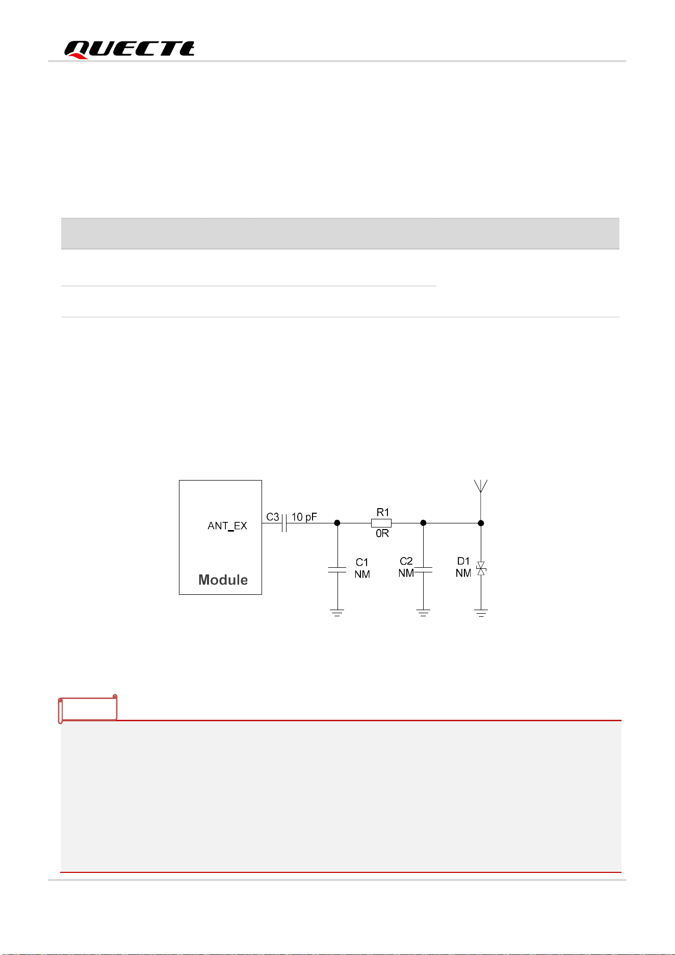
The circuit of pin antenna interface (ANT_EX) is shown below. For better RF performance, it is recommended to
reserve a dual-L type circuit and an ESD protection component. Components (R1, C1, C2, C3 and D1) of the dual-
L type circuit should be placed as close to the antenna as possible. C1, C2 and D1 are not mounted by default and
a 0 Ω resistor is mounted on R1.
Figure 8: Reference Design of Antenna Interface (ANT_EX)
1.It is recommended to reserve an ESD protection component for the antenna interface and the junction
capacitance should not exceed 0.05 pF.
2.Notes on C3:
1) If there is DC power at the antenna port, place a capacitor on C3 to prevent short circuit to ground. The
capacitance value is recommended to be 10 pF, which can be adjusted according to the debugging
results.
2) If there is no DC power in the peripheral design:
a) Do not reserve C3.
Pin Name Pin No. I/O Description Comment
ANT_IN 7 AIO
Bluetooth antenna interface
(module internal antenna)
50 Ω impedance.
ANT_EX 8 AIO Bluetooth Antenna Interface
NOTE
Sh
ort-Range Products
HSM110XC_Hardware_Design
28 / 53
b) If C3 has already been reserved, it should be mounted with a component, and it is recommended to
use a 0 Ω resistor. You can also match the components according to the debugging results.
5.2.3. RF Routing Guidelines
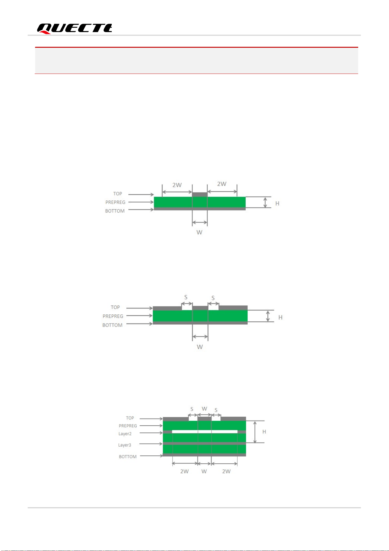
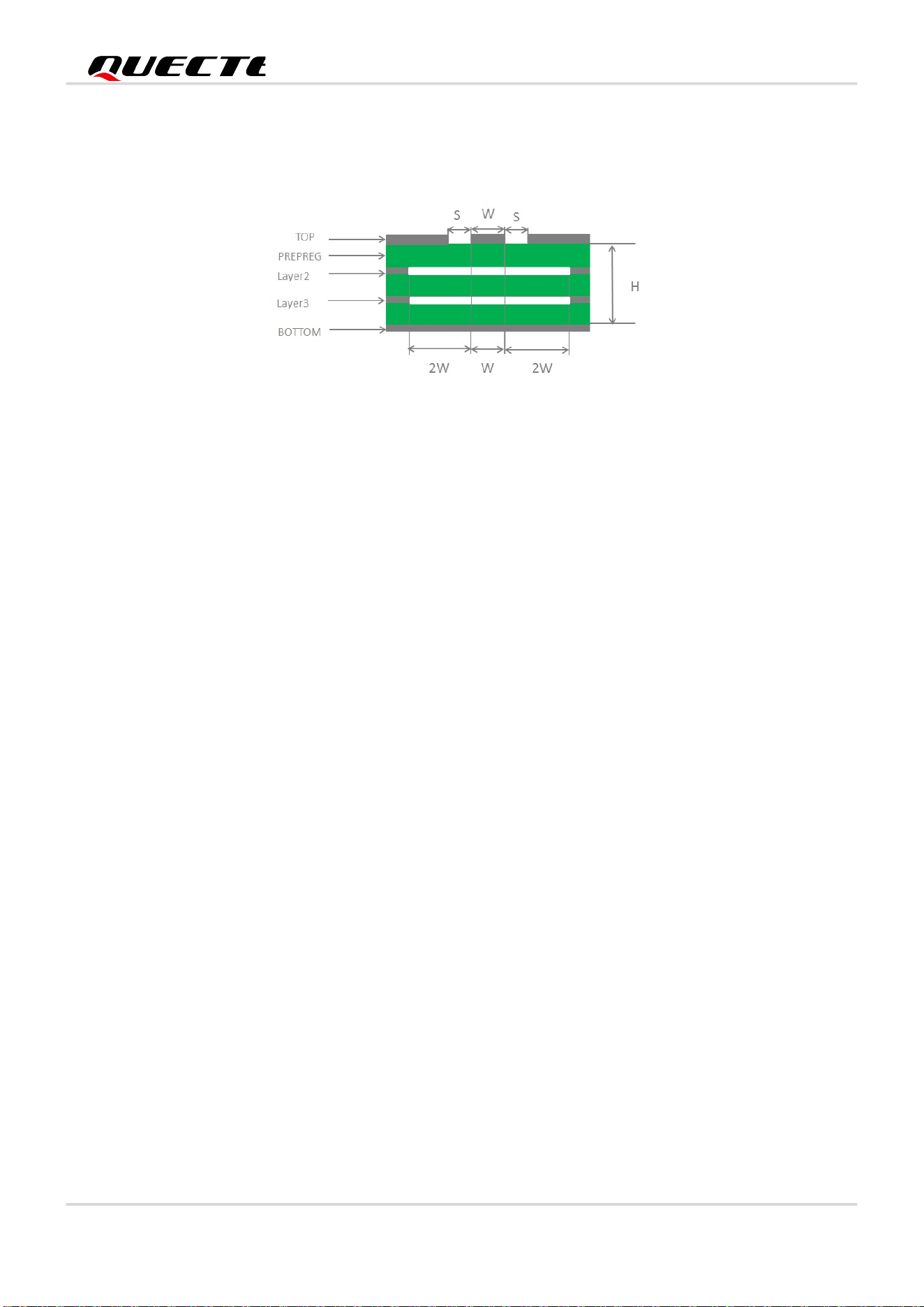
For user’s PCB, the characteristic impedance of all RF traces should be controlled to 50 Ω. The impedance of the
RF traces is usually determined by the trace width (W), the materials’ dielectric constant, the height from the
reference ground to the signal layer (H), and the spacing between RF traces and grounds (S). Microstrip or coplanar
waveguide is typically used in RF layout to control characteristic impedance. The following are reference designs
of microstrip or coplanar waveguide with different PCB structures.
Figure 9: Microstrip Design on a 2-layer PCB
Figure 10: Coplanar Waveguide Design on a 2-layer PCB
Sh
ort-Range Products
HSM110XC_Hardware_Design
29 / 53
Figure 11: Coplanar Waveguide Design on a 4-layer PCB (Layer 3 as Reference Ground)
Figure 12: Coplanar Waveguide Design on a 4-layer PCB (Layer 4 as Reference Ground)
To ensure RF performance and reliability, follow the principles below in RF layout design:
Use an impedance simulation tool to accurately control the characteristic impedance of RF traces to 50 Ω.
The GND pins adjacent to RF pins should not be designed as thermal relief pads, and should be fully
connected to ground.
The distance between the RF pins and the RF connector should be as short as possible and all the right-angle
traces should be changed to curved ones. The recommended trace angle is 135°.
There should be clearance under the signal pin of the antenna connector or solder joint.
The reference ground of RF traces should be complete. Meanwhile, adding some ground vias around RF traces
and the reference ground could help to improve RF performance. The distance between the ground vias and
RF traces should be at least twice the width of RF signal traces (2 × W).
Keep RF traces away from interference sources (such as DC-DC, (U)SIM/USB/SDIO high frequency digital
signals, display signals, and clock signals), and avoid intersection and paralleling between traces on adjacent
layers.
For more details about RF layout, see document [2].
5.2.4. RF Connector Recommendation
5.2.4.1. Antenna Connector Specifications
The mechanical dimensions of the receptacle are as follows.
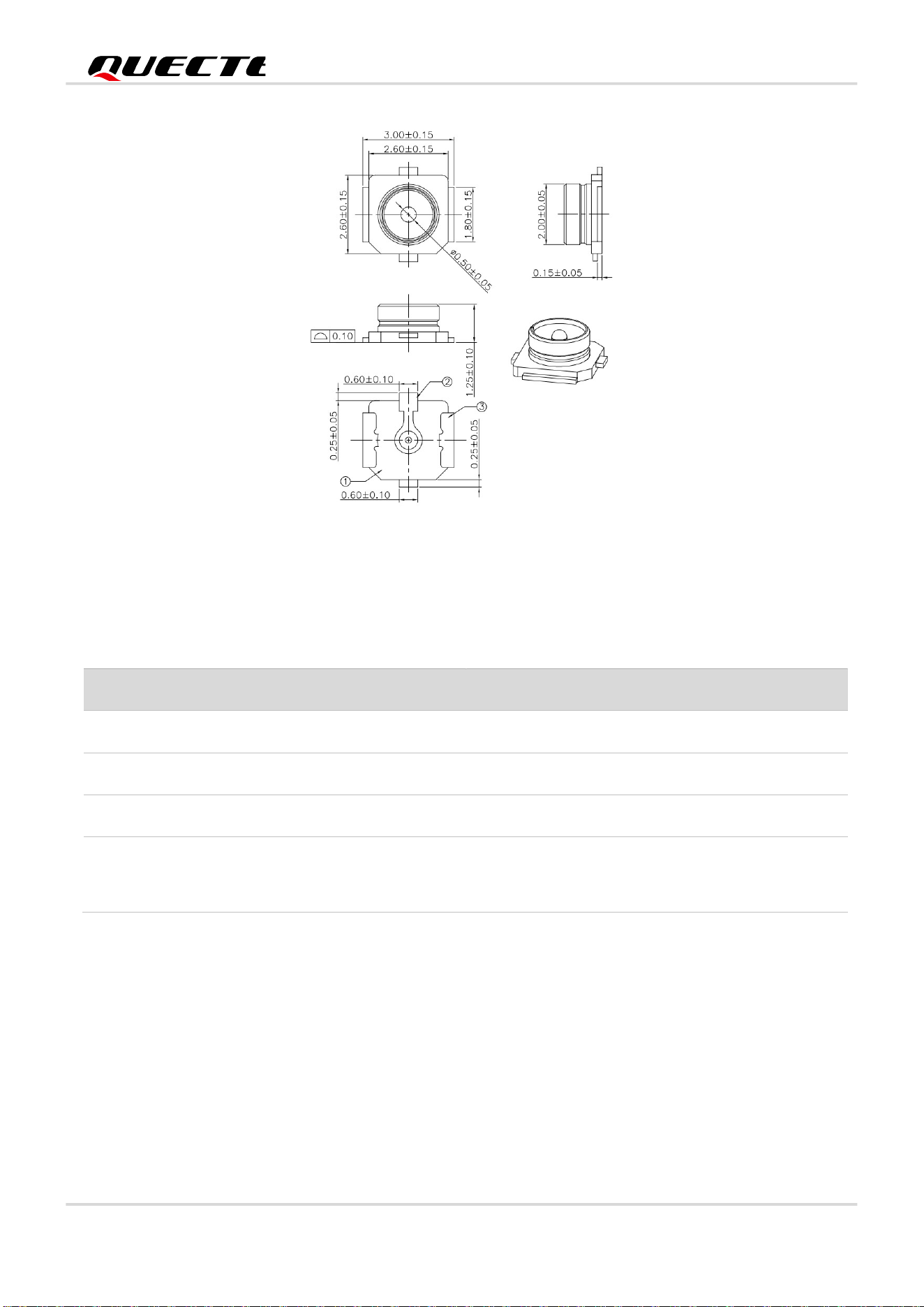
Sh
ort-Range Products
HSM110XC_Hardware_Design
30 / 53
Figure 13: Dimensions of the Receptacle (Unit: mm)
Table 15: Major Specifications of the RF Connector
5.2.4.2. Antenna Connector Installation
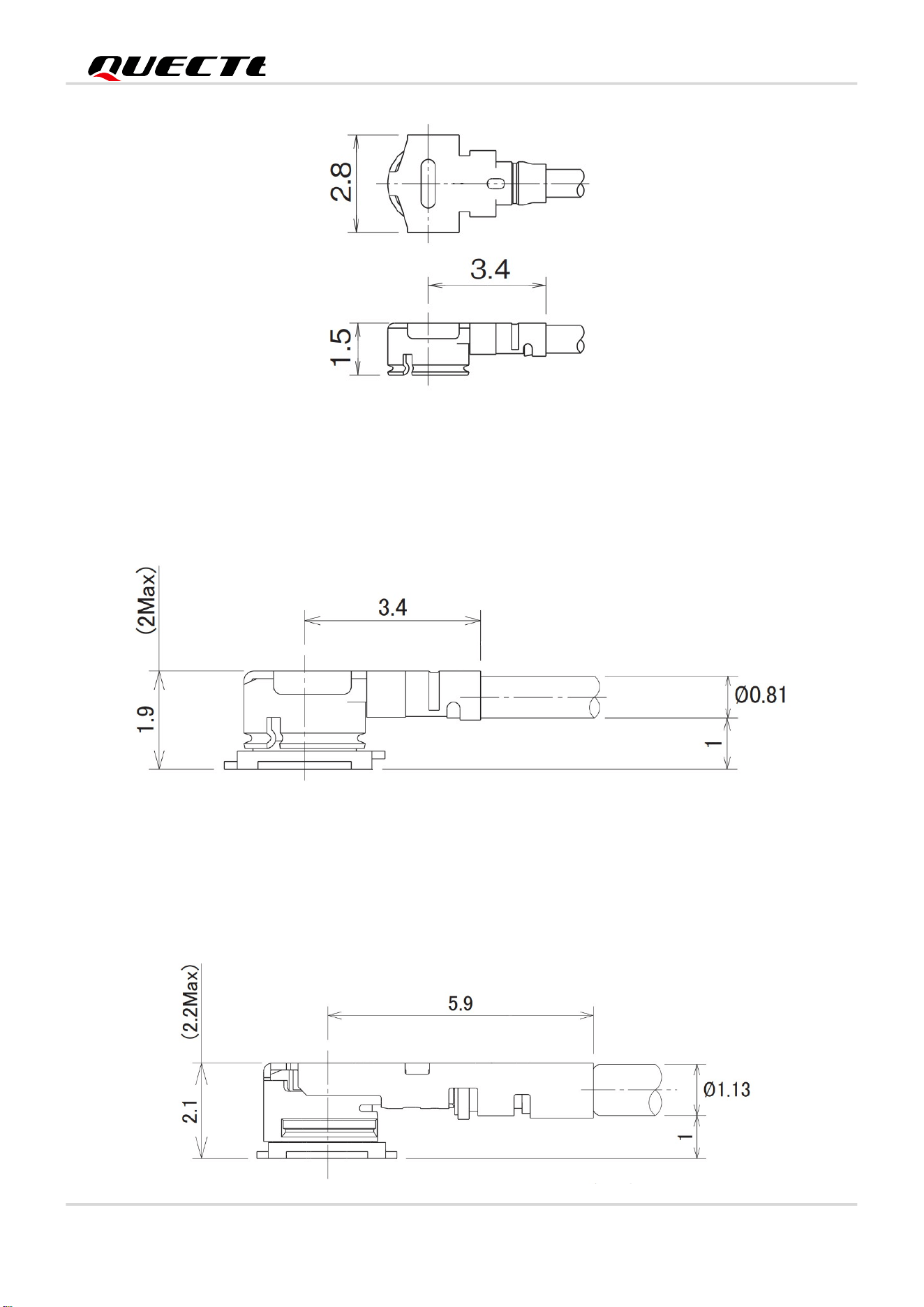
The receptacle used in conjunction with the module will accept two types of mated plugs that will meet a
maximum height of 2.0 mm using a Ø 0.81 mm coaxial cable or a maximum height of 2.2 mm utilizing a Ø 1.13
mm coaxial cable.
The following figure shows the dimensions of mated plugs using a Ø 0.81 mm/Ø 1.13 mm coaxial cable.
Parameter Specification
Nominal Frequency Range DC to 6 GHz
Nominal Impedance
50 Ω
Temperature Ranges
-40 °C to +85 °C
Voltage Standing Wave Ratio (VSWR)
Meet the following requirements:
Max. 1.3 (DC–3 GHz)
Max. 1.45 (3–6 GHz)
Sh
ort-Range Products
HSM110XC_Hardware_Design
31 / 53
Figure 14: Dimensions of the Receptacle (Unit: mm)
The following figure illustrates the connection between the receptacle on the module and the mated plug using a Ø
0.81 mm coaxial cable.
Figure 15: Space Factor of Mated Connectors (Ø 0.81 mm Coaxial Cables) (Unit: mm)
The following figure illustrates the connection between the receptacle on the module and the mated plug using a Ø
1.13 mm coaxial cable.
Sh
ort-Range Products
HSM110XC_Hardware_Design
32 / 53
Figure 16: Space Factor of Mated Connectors (Ø 1.13 mm Coaxial Cables) (Unit: mm)
5.2.4.3. Recommended Manufacturers of RF Connector and Cable
RF connectors and cables by I-PEX are recommended. For more details, visit https://www.i-pex.com.
5.2.5. Requirements for Antenna Design
Table 16: Requirements for Antenna Design
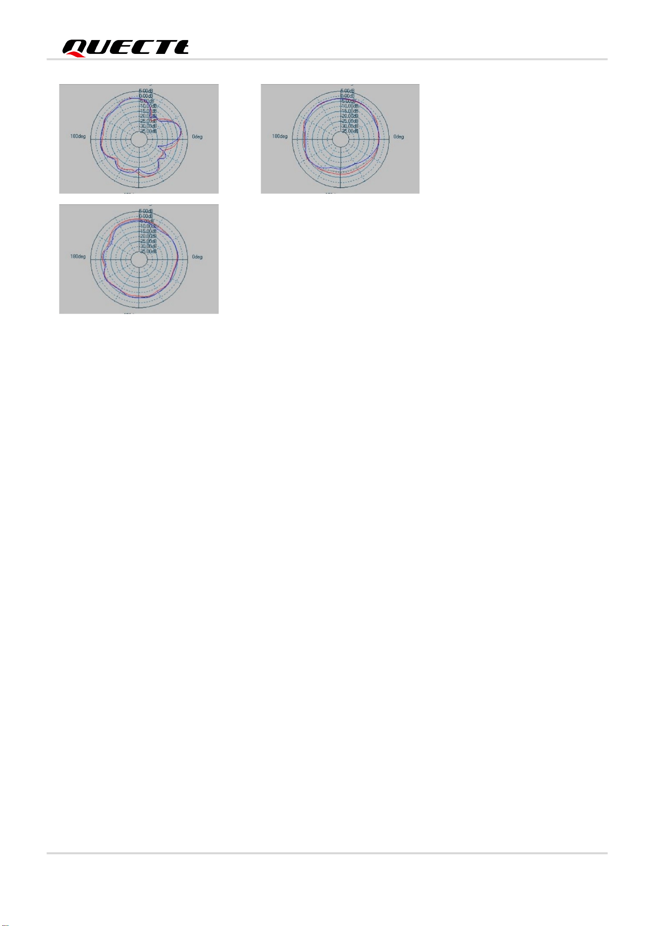
5.2.6. Antenna Direction Diagram
X-Y Plane X-
Y Plane
X-Z Plane
Parameter Requirements
Frequency Range (GHz)
2.4 GHz: 2.400–2.4835
Loss (dB) < 1
Input Impedance (Ω)
50 (Typ.)
VSWR
≤ 2 (Typ.)
Gain (dBi) 1 (Typ.)
Polarization Vertical
Sh
ort-Range Products
HSM110XC_Hardware_Design
33 / 53
Figure 17: Antenna Direction Diagram
Sh
ort-Range Products
HSM110XC_Hardware_Design
34 / 53
6 Electrical Characteristics and
Reliability
6.1. Absolute Maximum Ratings
Table 17: Absolute Maximum Ratings (Unit: V)
Exceeding the conditions of use as shown above may cause permanent damage to the module.
6.2. Power Supply Ratings
Table 18: Module’s Power Supply Ratings (Unit: V)
Parameter Min. Max.
VBAT -0.3 3.9
Voltage at digital pins -0.3 3.9
ADC Input voltage 0 3.9
Parameter Description Condition Min. Typ. Max.
VBAT
Power supply
for the module
The actual input voltages must be
kept between the minimum and
maximum values
1.71 3.3 3.6
NOTE

Sh
ort-Range Products
HSM110XC_Hardware_Design
35 / 53
6.3. Bluetooth Power Consumption
Test conditions for module power consumption are as follows:
An ambient temperature of 25 °C
Typical power domain
50 Ω impedance
The following power consumption data are for your reference only. Actual values may vary among different
modules due to differences in internal components, software versions and test ambient temperatures. For more
details, please contact Quectel Technical Support.
Table 19: Bluetooth Power Consumption (Unit: mA; Max.)
Table 20: Power Consumption in Sleep Mode (Unit: μA; Typ.)
Condition I
VBAT
RX 3.4
TX Power: 20 dBm 3.6
TX Power: 0 dBm 4.2
TX Power: +4 dBm 5.5
TX Power: +7.5 dBm 8.5
Beacon broadcasting, interval: 1 s, 23 bytes, 0 dBm
10 μA
Power Supply
Mode
32 KHz RCOSC SRAM retention Wakeup Mode
Power
Consumption
Turn-off OFF OFF GPIO wake-up 0.6
Sleep Mode
ON 16 KB RAM
GPIO wake-up and clock
wake-up
1.2
ON 80 KB RAM
GPIO wake-up and clock
wake-up
1.7

Sh
ort-Range Products
HSM110XC_Hardware_Design
36 / 53
6.4. Digital I/O Characteristics
Table 21: VBAT I/O Characteristics (Unit: V)
6.5. ESD Protection
Static electricity occurs naturally and it may damage the module. Therefore, applying proper ESD
countermeasures and handling methods is imperative. For example, wear anti-static gloves during the
development, production, assembly and testing of the module; add ESD protection components to the ESD
sensitive interfaces and points in the product design.
Table 22: Electrostatic Discharge Characteristics (Unit: kV)
Parameter Description Min. Max.
V
IH
High-level input voltage
0.7 × VBAT
VBAT + 0.3
V
IL
Low-level input voltage -0.3
0.3 × VBAT
V
OH
High-level output voltage
0.9 × VBAT
-
V
OL
Low-level output voltage -
0.1 × VBAT
Model Test Result Reference Standard
Human Body Model
±4
ESDA/JEDEC JS-001-2017
Charge Device Model
±1
ESDA/JEDEC JS-002-2018
Sh
ort-Range Products
HSM110XC_Hardware_Design
37 / 53
7 Mechanical Information
This chapter describes the mechanical dimensions of the module. All dimensions are measured in millimeter (mm),
and the dimensional tolerances are ±0.1 mm unless otherwise specified.
7.1. Mechanical Dimensions
Figure 18: Top and Side Dimensions
Sh
ort-Range Products
HSM110XC_Hardware_Design
38 / 53
7.2. Recommended Footprint
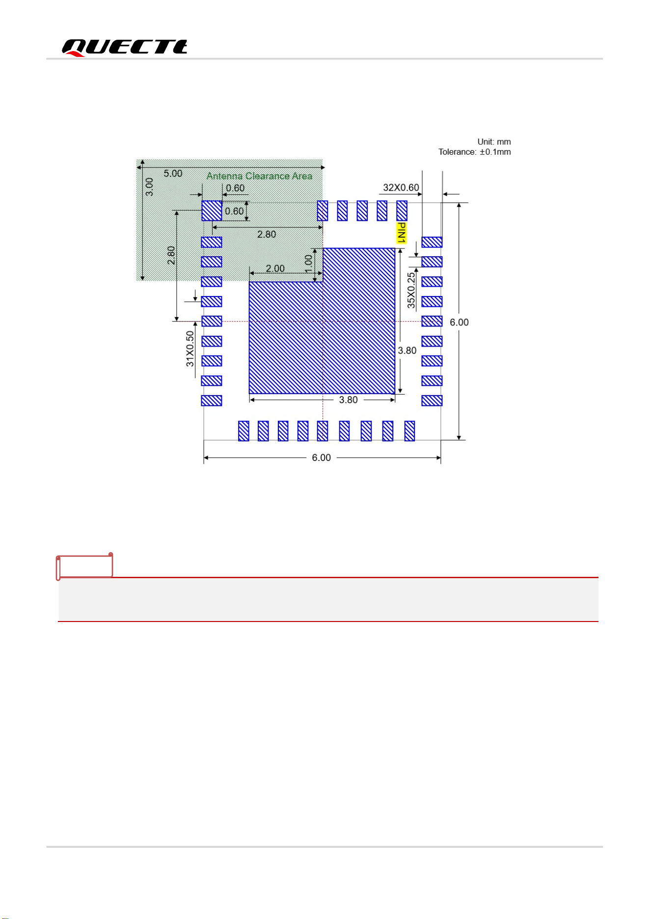
Figure 19: Recommended Footprint
Keep at least 2 mm between the module and other components on the motherboard to improve soldering quality
and maintenance convenience.
NOTE
Sh
ort-Range Products
HSM110XC_Hardware_Design
39 / 53
7.3. Top View
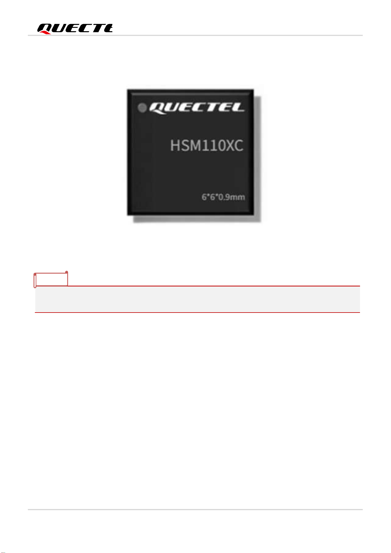
Figure 20: Top View
Image above is for illustration purpose only and may differ from the actual module. For authentic appearance and
label, please refer to the module received from Quectel.
NOTE
Sh
ort-Range Products
HSM110XC_Hardware_Design
40 / 53
8 Storage, Manufacturing and
Packaging
8.1. Storage Conditions
The storage/shelf life of the module in a vacuum-sealed packaging is 12 months under conditions of temperature <
40 °C and relative humidity < 90%.
1. To avoid blistering, layer separation and other soldering issues, extended exposure of the module to the air is
forbidden.
2. Take out the module from the package and put it on high-temperature-resistant fixtures before baking. If
shorter baking time is desired, see IPC/JEDEC J-STD-033 for the baking procedure.
3. Pay attention to ESD protection, such as wearing anti-static gloves, when touching the modules.
8.2. Manufacturing and Soldering
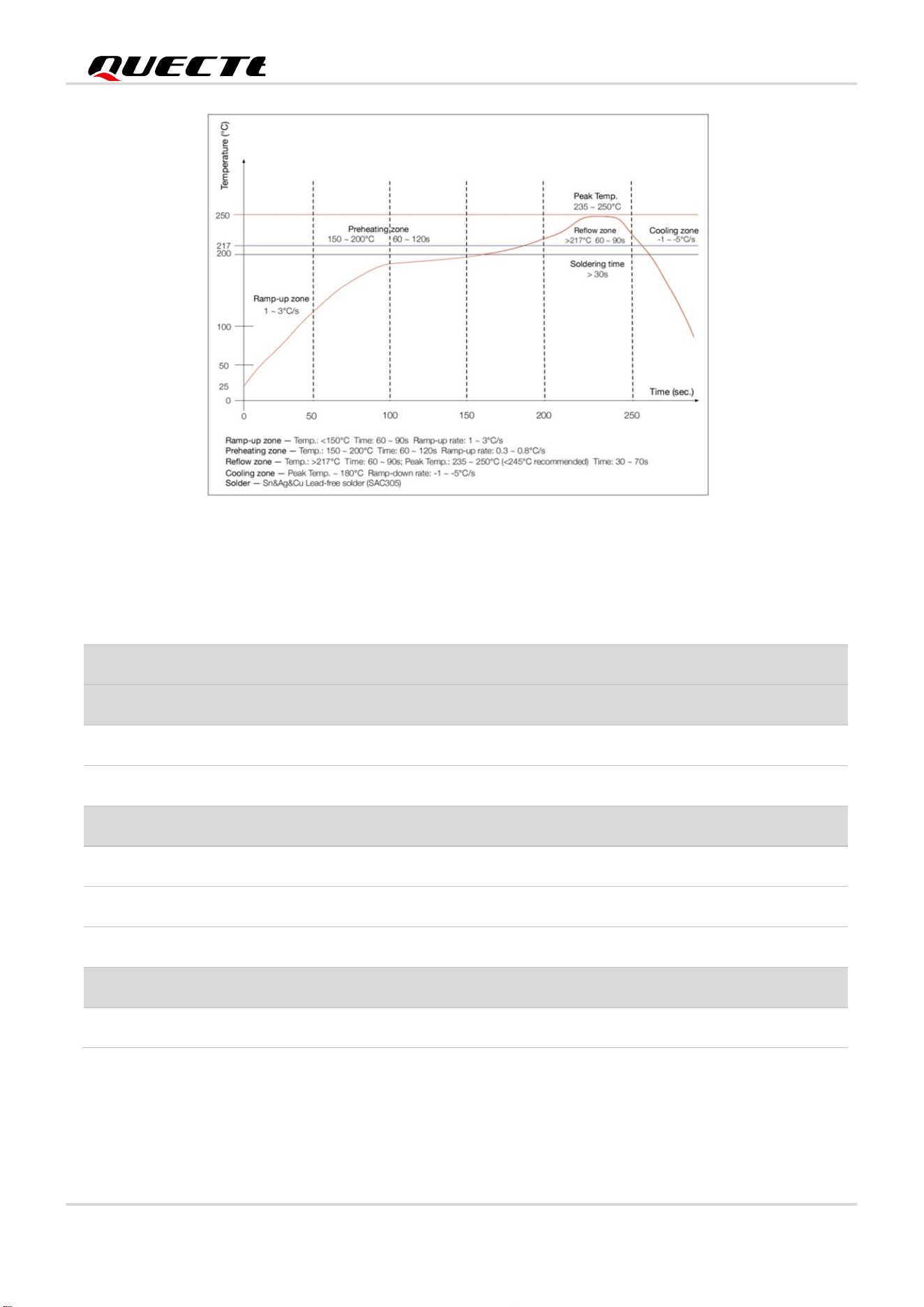
The recommended peak reflow temperature should be 235–245 ºC, with 250 ºC as the absolute maximum reflow
temperature. To avoid damage to the module caused by repeated heating, it is recommended that the module
should be mounted only after reflow soldering for the other side of PCB has been completed. The recommended
reflow soldering thermal profile (lead-free reflow soldering) and related parameters are shown below. It is
recommended to use a reflow oven with over 10 temperature zones.
NOTE
Sh
ort-Range Products
HSM110XC_Hardware_Design
41 / 53
Figure 21: Recommended Reflow Soldering Thermal Profile
Table 23: Recommended Thermal Profile Parameters
Factor Recommended Value
Ramp-up Zone
Ramp-to-soak Slope
1–3 °C/s
Ramp-up Time
60–90 s
Reflow Zone
Reflow Time (D: over 217°C) 60–90 s
Max Temperature
235–250 °C
Cool-down Slope
-1–-5 °C/s
Reflow Cycle
Max Reflow Cycle 1
Sh
ort-Range Products
HSM110XC_Hardware_Design
42 / 53
8.3. Packaging Specifications
This chapter outlines the key packaging parameters and processes. All figures below are for reference purposes
only, as the actual appearance and structure of packaging materials may vary in delivery.
The modules are packed in a tape and reel packaging as specified in the sub-chapters below.
8.3.1. Carrier Tape
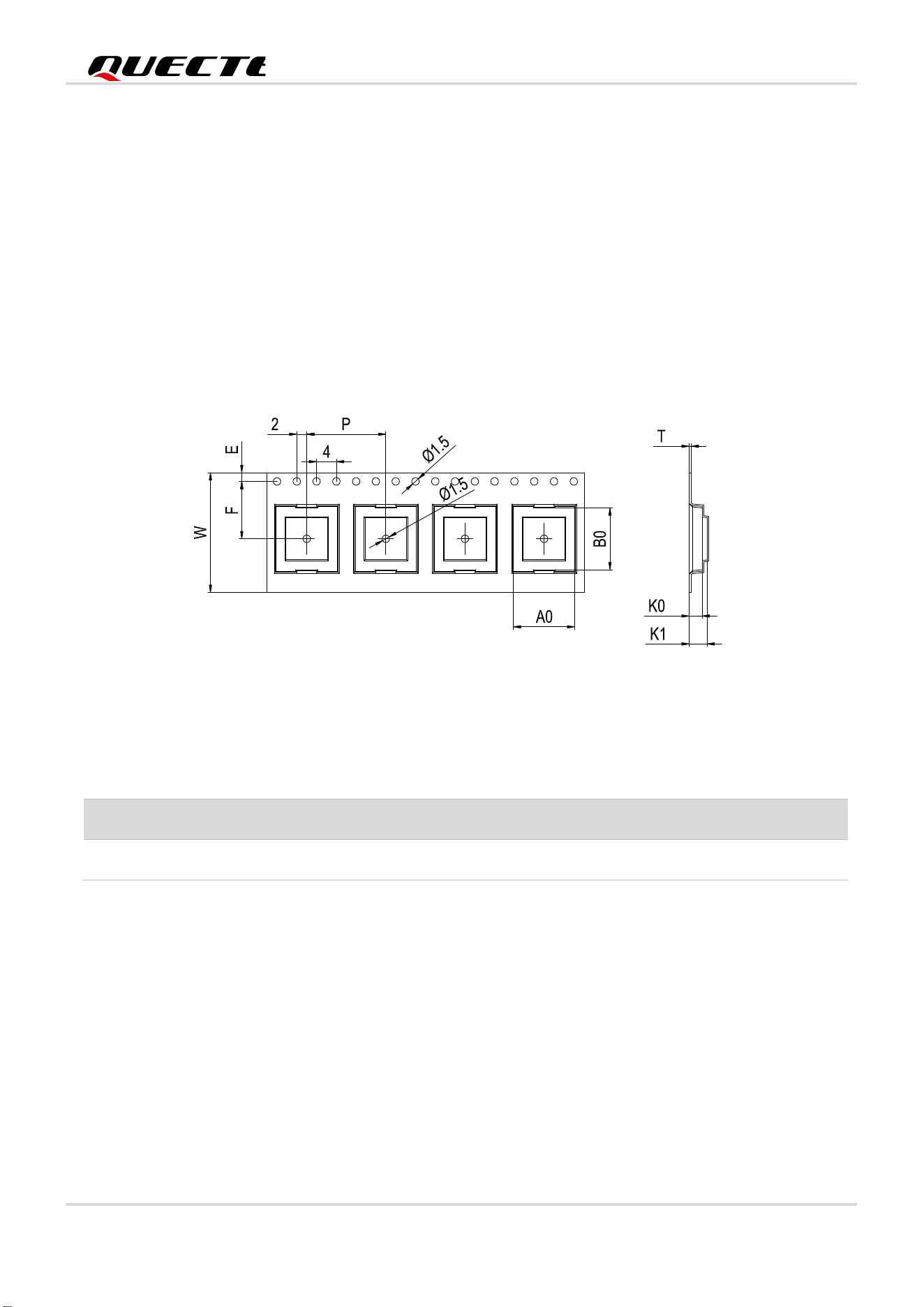
Carrier tape dimensions are illustrated in the following figure and table:
Figure 22: Carrier Tape Dimension Drawing (Unit: mm)
Table 24: Carrier Tape Dimension Table (Unit: mm)
W P T A0 B0 K0 K1 F E
16 12 0.3 6.3 6.3 1.1 - 7.5 1.75
Sh
ort-Range Products
HSM110XC_Hardware_Design
43 / 53
8.3.2. Plastic Reel
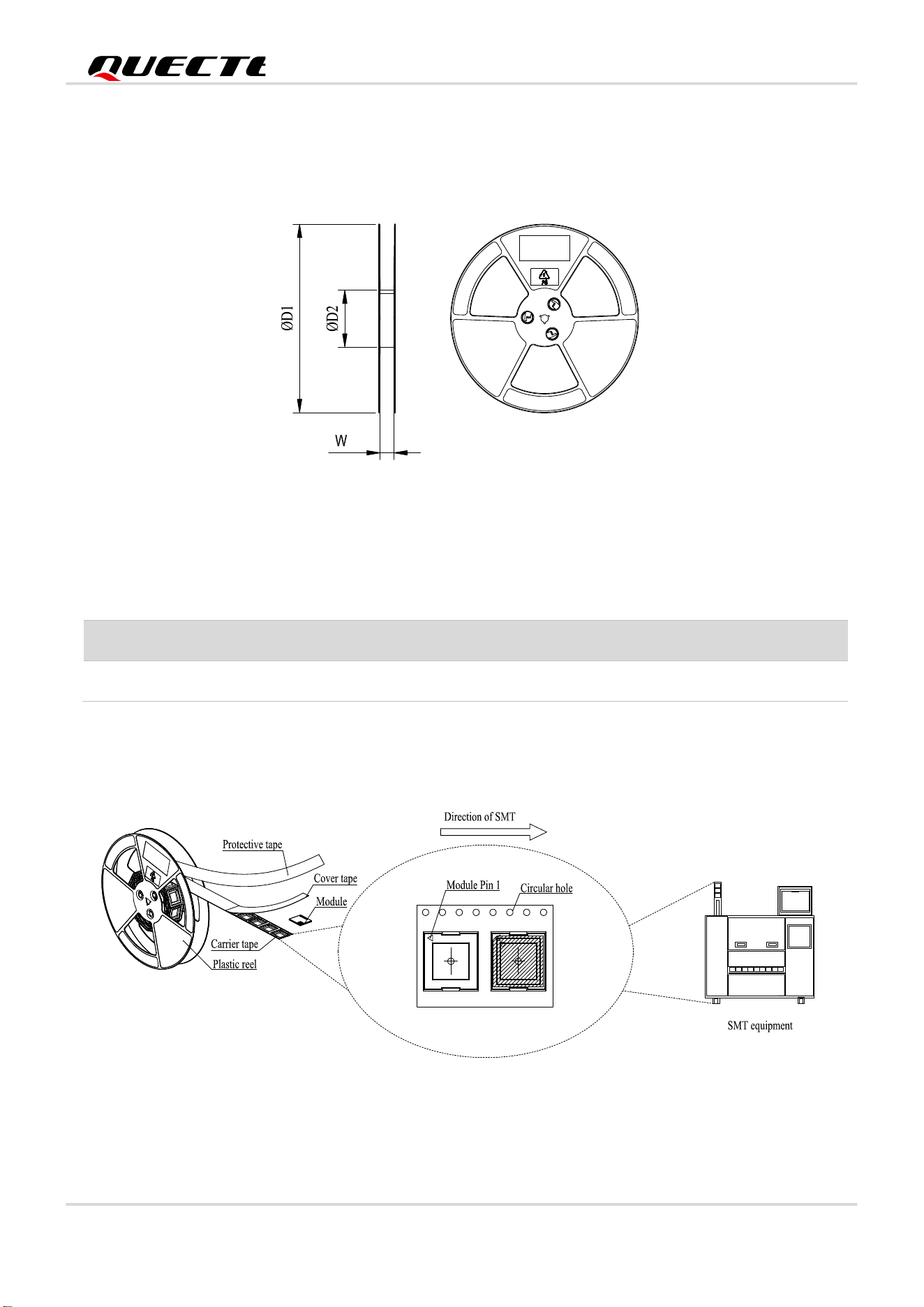
Plastic reel dimensions are illustrated in the following figure and table:
Figure 23: Plastic Reel Dimension Drawing
Table 25: Plastic Reel Dimension Table (Unit: mm)
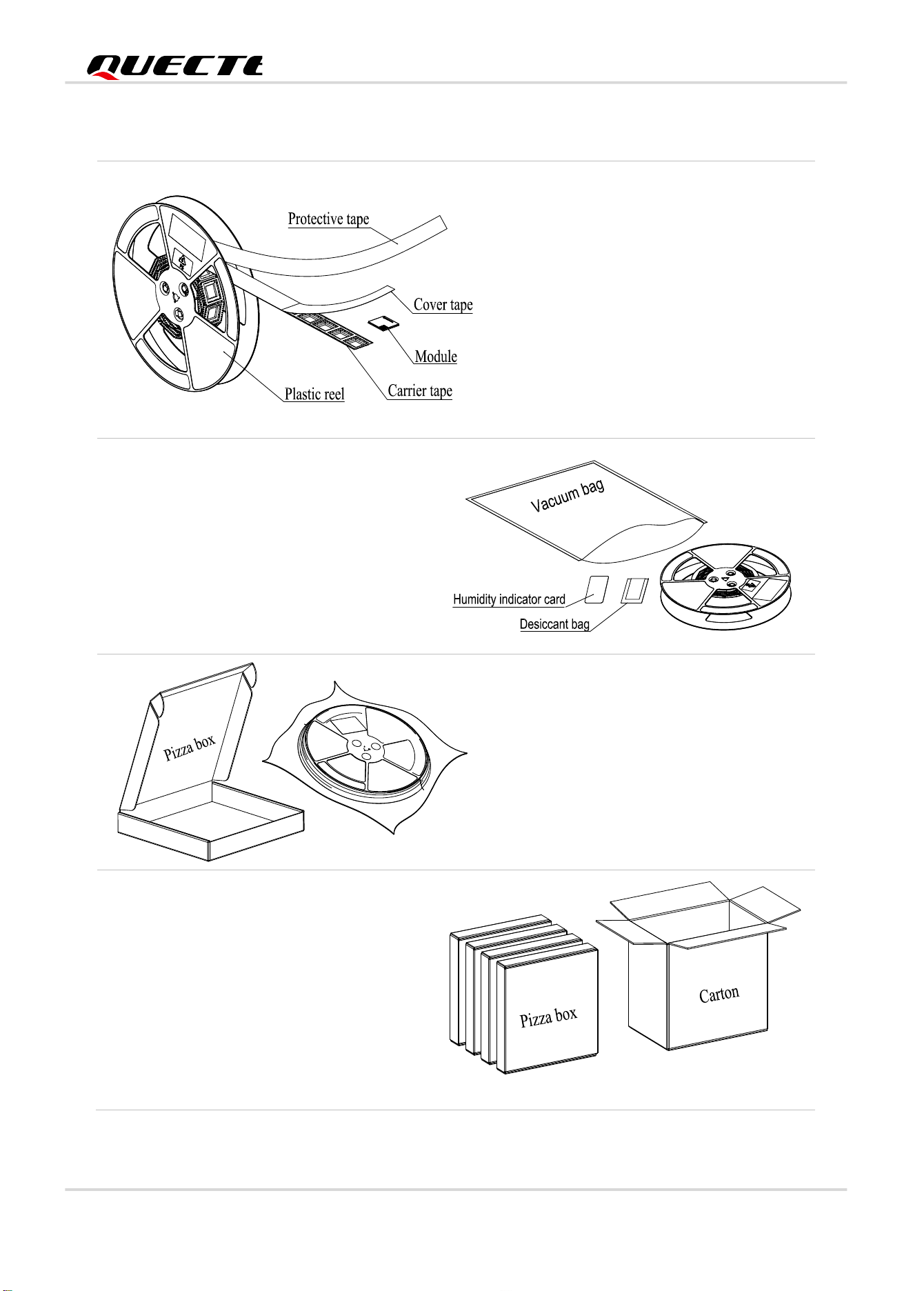
8.3.3. Mounting Direction
Figure 24: Mounting Direction
øD1 øD2 W
330 100 16
Sh
ort-Range Products
HSM110XC_Hardware_Design
44 / 53
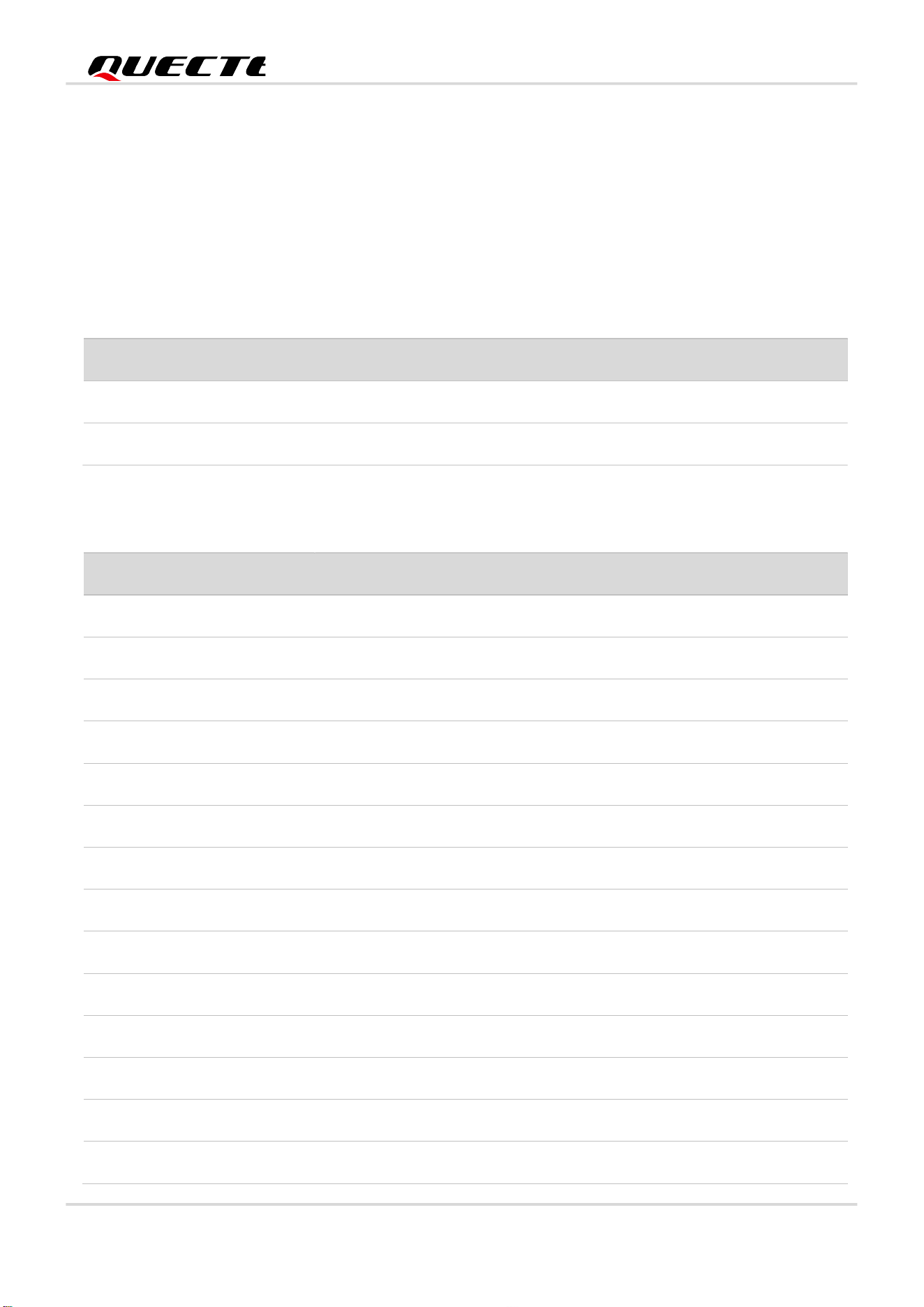
8.3.4. Packaging Process
Place the modules onto the carrier tape cavity
and cover them securely with cover tape. Wind
the heat-sealed carrier tape onto a plastic reel
and apply a protective tape for additional
protection. 1 plastic reel can pack 3000
modules.
Place the packaged plastic reel, humidity
indicator card and desiccant bag into a vacuum
bag, and vacuumize it.
Place the vacuum-packed plastic reel into a
pizza box.
Place the 4 packaged pizza boxes into 1 carton
and seal it. 1 carton can pack 12000 modules.
Figure 25: Packaging Process
Sh
ort-Range Products
HSM110XC_Hardware_Design
45 / 53
9 Appendix References
Table 26: Related Documents
Table 27: Terms and Abbreviations
Document Name
[1] Quectel_HSM110XC_TE-B_User_Guide
[2] Quectel_RF_Layout_Application_Note
Abbreviation Description
ARM Advanced RISC Machine
BLE Bluetooth Low Energy
DMA Direct Memory Access
EFUSE Electronic Fuse
ESD Electrostatic Discharge
GFSK Gauss Frequency Shift Keying
GND Ground
GPIO General-Purpose Input/Output
I/O Input/Output
I2C Inter-Integrated Circuit
I2S Inter-IC Sound
Mbps Million Bits Per Second
MCU Microcontroller Unit
PCB Printed Circuit Board

Sh
ort-Range Products
HSM110XC_Hardware_Design
46 / 53
PWM Pulse Width Modulation
RAM Random-Access Memory
RCOSC Resistor-Capacitor Oscillator
RF Radio Frequency
RoHS Restriction of Hazardous Substances
SIP System in Package
SPI Serial Peripheral Interface
SRAM Static Random-Access Memory
TVS Transient Voltage Suppressor
UART Universal Asynchronous Receiver/Transmitter
V
IH
High-level Input Voltage
V
IL
Low-level Input Voltage
Vmax Maximum Voltage
Vmin Minimum Voltage
Vnom Nominal Voltage
V
OH
High-level Output Voltage
V
OL
Low-level Output Voltage
VSWR Voltage Standing Wave Ratio

Sh
ort-Range Products
HSM110XC_Hardware_Design
47 / 53
FCC Statement FCC ID: XMRHSM110XC
Warning: Changes or modifications to this unit not expressly approved by the party responsible
for compliance could void the user’s authority to operate the equipment.
NOTE: This equipment has been tested and found to comply with the limits for a Class B digital
device, pursuant to Part 15 of the FCC Rules. These limits are designed to provide reasonable
protection against harmful interference in a residential installation. This equipment generates, uses
and can radiate radio frequency energy and, if not installed and used in accordance with the
instructions, may cause harmful interference to radio communications.
However, there is no guarantee that interference will not occur in a particular installation. If this
equipment does cause harmful interference to radio or television reception, which can be
determined by turning the equipment off and on, the user is encouraged to try to correct the
interference by one or more of the following measures:
Reorient or relocate the receiving antenna.
Increase the separation between the equipment and receiver.
Connect the equipment into an outlet on a circuit different from that to which
the receiver is connected.
Consult the dealer or an experienced radio/TV technician for help
The device must not be co-located or operating in conjunction with any other antenna or transmitter.
This device complies with Part 15 of the FCC Rules. Operation is subject to the following two
conditions : (1) this device may not cause harmful interference, and (2) this device must accept any
interference received, including interference that may cause undesired operation.
FCC Radiation Exposure Statement
This equipment should be installed and operated with minimum distance 20cm between the
radiator and your body.
Does not comply with the use restrictions of the product:
Portable devices used close with human’s body (within 20cm), Like Cell phone, Notebook etc.

Sh
ort-Range Products
HSM110XC_Hardware_Design
48 / 53
Note: This module has no RF shield. Un‑shielded circuitry may cause receiver performance
degradation or end‑product emission risks. Host integrator is responsible for layout, mitigation and
end‑product compliance.
1. General Compliance Statement
This wireless module has obtained FCC modular certification in accordance with 47 CFR Part
15.212 and KDB 996369 D03 V01. The module is a standalone radio frequency transmitting device.
All integration and application behaviors of the host integrator must strictly comply with the
specifications in this manual. Any integration beyond the authorized scope will automatically
invalidate the FCC certification of the module.
2. Applicable FCC Rules (KDB 996369 D03-2.2)
This modular transmitter is authorized under Applicable FCC Part 15 Subpart C 15.247 & 15.209 .
Important Note: The module FCC grant only covers the intentional radiator performance of the
module. It does not extend the Part 15B unintentional radiator compliance to the final host system.
The OEM host integrator shall independently complete the Part 15B EMI test and compliance
certification for the complete host product.
3. Specific Operational Integration Conditions (KDB 996369
D03-2.3)
All host integration and application scenarios must meet the following fixed conditions. No
unauthorized modification is allowed.
1. Application Scenario Restriction: The module is only allowed to be installed in fixed or
mobile host devices. Integration and use in portable handheld, wearable body-worn devices are
prohibited without additional FCC authorization.
2. Power Supply Specification: The host device shall provide a stable rated working voltage of
3.3 V for the module. The module is equipped with a built-in power regulation circuit. The host shall
not modify, replace or reconstruct the module power supply circuit and peripheral power distribution
structure.
3. Hardware & Signal Restriction: The module PCB layout, shielding structure, component layout
and signal input interface are fixed and certified. The host shall not modify PCB wiring, remove

Sh
ort-Range Products
HSM110XC_Hardware_Design
49 / 53
shielding parts, alter component parameters, or amplify/remodulate RF-related signal input. All
hardware and firmware modifications are strictly prohibited.
4. Co-location Restriction: This transmitter shall not be co-located or operated simultaneously
with any other radio transmitters, antennas or RF modules in the same host device, unless the host
completes official FCC multi-transmitter co-location evaluation and obtains approval.
4. Limited Module Special Provisions
Important Limited Module Mandatory Rule: This product is a FCC limited modular transmitter, and
the following provisions are mandatory and shall not be omitted.
If this is a limited modular transmitter, the host OEM integrator must obtain written integration
approval from the module grantee before integrating the module into any host product. For new
host model integration, the integrator shall complete FCC Class-II Permissive Change filing and
approval.
6. RF Exposure Compliance Requirements (KDB 996369 D03-
2.6)
1. The certified minimum separation distance between the module antenna and human body is 20
cm. The host mechanical and structural design must ensure that this safety distance is always
maintained during normal device operation.
2. The module RF exposure evaluation is only applicable to fixed and mobile device scenarios. If
the module is integrated into portable body-worn devices with a working distance less than 20cm,
the host integrator must complete independent SAR testing and FCC RF exposure certification.
3. The host final product user manual must be added with official RF exposure warning statements
to meet FCC regulatory requirements.
Recommended End-user Manual RF Exposure Statement
This equipment complies with FCC RF radiation exposure limits set forth for an uncontrolled
environment. This equipment should be installed and operated with a minimum distance of 20 cm
between the radiator and your body.
7. Antenna Compliance Specifications (KDB 996369 D03-2.7)
Only the certified matching antenna can be used with this module. Unauthorized replacement and

Sh
ort-Range Products
HSM110XC_Hardware_Design
50 / 53
modification are prohibited.
Antenna Parameter Certified Specification
Antenna Type Chip antenna
Maximum Antenna Gain 1 dBi
Antenna Impedance
50Ω
Connector Type
RF connectors and cables by I-
PEX are recommended. For
more details, visit
https://www.i-pex.com
1. Generic vague descriptions (such as omnidirectional antenna) are not acceptable for FCC audit.
The antenna type must be clearly defined.
2. It is strictly prohibited to replace the antenna, adjust antenna gain, extend antenna cable, or add
antenna splitters and auxiliary antenna devices.
3. The host must use the certified fixed connector type, and no adaptive modification of the
interface is allowed.
8. Labeling Compliance Requirements (KDB 996369 D03-2.8)
1. The module shall retain the original permanent FCC ID label, which shall not be removed,
modified or covered.
2. The final host product shall be permanently and clearly marked with the statement: Contains
FCC ID: XMRHSM110XC. The marking can adopt physical label or electronic label that complies
with KDB 784748 specification.
3. The host product shall not independently use the module’s FCC ID as the host’s own certification
ID. All host-level compliance responsibilities are undertaken by the OEM integrator.
9. Testing & Verification Guidance (KDB 996369 D03-2.9)
1. The OEM integrator shall obtain the module RF test mode authority to verify the RF performance
after host integration.
2. After module integration, the host must complete independent Part 15B conducted and radiated

Sh
ort-Range Products
HSM110XC_Hardware_Design
51 / 53
emission tests for unintentional radiation.
3. If the host has multiple transmitters co-located, a complete multi-transmitter co-location
evaluation test must be performed.
4. If the host application scenario, power supply, antenna and other conditions exceed the module
certification authorization scope, the integrator must apply for FCC Class-II Permissive Change or
re-certification.
The test plan shall confirm and demonstrate compliance with the following:
Confirm and document the continued compliance for the fundamentals for each band under each specific
rule part granted for the module.
The test shall demonstrate each band's worst-case modulation mode(s).
Test band edge compliance for the widest and narrowest bandwidths per modulation type. Include
radiated spurious emissions with the antenna connected. Testing shall be performed for each supported
modulation testing 15.31(m). In all cases, a test of each modulation is required for channels over the
frequency range defined in 15.33(a) for unlicensed transmitters and 2.1057(a) for licensed transmitters.
Confirm and demonstrate with the radiated test that no additional parasitic, non-compliant emissions exist
due to ingress (parasitic oscillations, radiation of stray signals within a host, etc.) are present.
These tests can be based on C63.10 and C63.26 as guidance:
Examples: The devices that support Bluetooth LE all bandwidths, and data rates. Testing may be documented
for a limited selection of Bluetooth LE modes for worst-case GFSK subcarrier or tone arrangements. The
worst-case modes can be selected from the radio module's initial test report. The widest bandwidth, highest
aggregate power, and highest power spectral density should be tested. If these conditions do not all combine
in the same mode, then multiple modes require testing until the modes with these three parameters have been
tested and confirmed. Compliance testing is necessary if the manufacturer does not identify the worst-case
settings for each modulation and data rate.
10. Compliance Responsibility Division (KDB 996369 D03-2.10)
1. The module manufacturer (grantee) is only responsible for the standalone RF compliance of the
module itself, and is not responsible for any system-level compliance problems caused by host
improper integration.
2. The OEM host integrator bears full responsibility for all system-level compliance of the final
product, including but not limited to: host EMI/EMC compliance, Part15B compliance, RF
exposure/SAR evaluation, labeling compliance, multi-transmitter co-location compliance, and filing
of necessary permit changes.

Sh
ort-Range Products
HSM110XC_Hardware_Design
52 / 53
3. Any failure to follow this integration manual will result in the invalidation of the module’s FCC
certification in the host system, and all related risks and liabilities shall be borne by the host
integrator.
IC Statement IC:10224A-HSM110XC
This device complies with Industry Canada license-exempt RSS standard(s). Operation is subject
to the following two conditions: (1) this device may not cause interference, and (2) this device must
accept any interference, including interference that may cause undesired operation of the device.
Le présent appareil est conforme aux CNR d’Industrie Canada applicables aux appareils radio
exempts de licence. L’exploitation est autorisée aux deux conditions suivantes :(1) l’appareil ne
doit pas produire de brouillage, et (2) l’utilisateur de l’appareil doit accepter tout brouillage
radioélectrique subi, même si le brouillage est susceptible d’en compromettre le fonctionnement.
The device is compliance with RF field strength limits, users can obtain Canadian information on
RF exposure and compliance.
IC Radiation Exposure Statement
This equipment complies with IC radiation exposure limits set forth for an uncontrolled
environment. This equipment should be installed and operated with minimum distance 20cm
between the radiator & your body.
Déclaration d’exposition aux radiations:

Sh
ort-Range Products
HSM110XC_Hardware_Design
53 / 53
Cet équipement est conforme aux limites d’exposition aux rayonnements IC établies pour un
environnement non contrôlé. Cet équipement doit être installé et utilisé avec un minimum de 20
cm de distance entre la source de rayonnement et votre corps.
The Bluetooth module is designed to comply with the ISED statement. The module ID is 10224A-
HSM110XC. The host system using HSM110XC, should have label indicatedit contain modular's
IC :10224A-HSM110XC.This radio module must not installed to co-locate and operating
simultaneously with otherradios in host system, additional testing and equipment authorization
should be requiredto operating simultaneously with other radio.Le module HSM110XC est concu
pour se conformer a la declaration ISDE. Le numerod'identification du module est 10224A-
HSM110XC tte indiquant qu'il contient I'IC modulaire: 10224A-HSM110XC.Ce module radio ne doit
pas etre installe pour co-localiser et fonctionner simultanementavec d'autres radios dans le
systeme hote, des tests supplementaires et une autorisationd'equipement peuvent etre
necessaires pour fonctionner simultanement avec d'autresradios.
End Product Labeling
This transmitter module is authorized only for use in device where the antenna may be installed such that20
cm may be maintained between the antenna and users. The final end product must belabeled in a visible area
with the following: “Contains IC:10224A-HSM110XC".
Étiquetage du produit final
Ce module émetteur n’est autorisé que pour une utilisation dans un dispositif où l’antenne peut être installée
de telle sorte que 20 cm puissent être maintenus entre l’antenne et les utilisateurs. Le produit final doit être
étiqueté dans une zone visible avec la mention suivante: “contient IC:10224A-HSM110XC”.
PMN: QUECTEL HSM110XC