
———————————————————————————————————————————————————————————————————
User Manual

———————————————————————————————————————————————————————————————————
1. Features
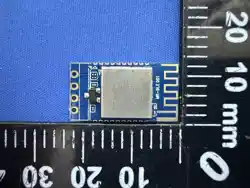
MR-BLE001 is a small-sized, low-cost Bluetooth BLE standard transparent
transmission module developed by Yulu. The module supports BLE (Up to Bluetooth
5.0). The built-in 512kB FLASH supports dynamic stack and protocol profile
configuration, and product functions can be configured through software, providing
ultimate flexibility. Both hardware OTA upgrades and multi-boot switching are
supported, allowing for convenient product feature rollouts and upgrades.
The module features are as follows:
▶Built-in high performance 32-bit MCU RSIC @48M ,512KB Flash,32KB SRAM
▶Compliant with Bluetooth 5.0, RF link data up to 2Mbps
▶transmit power:
▶Support UART interface, expand all I/O ports of the chip
▶Support APP parameter configuration
▶Stamp hole pin + 4pin terminal interface, easy and reliable welding
▶Ultra-small package: 23x12.6mm, board thickness 1.0mm
▶Working temperature: -40℃~+85℃
The MR-BLE001 module only needs to connect VCC, GND, TX, RX four wires to
complete the data transparent transmission function; it can also be applied to many
small-sized accessories or fitness products through the stamp hole. It can easily realize
the interconnection of users' Bluetooth devices, data transmission and other various
applications.
2.2dBm

———————————————————————————————————————————————————————————————————
1.1 Application field
▶Smart jump rope, abdominal wheel and other fitness accessories
▶Smart treadmill, spinning bike and other fitness equipment
▶Smart Home Products
▶Industrial control equipment
2 Electrical Specifications
█Rated parameters
Notice:
1) The listed electrical characteristics are target specifications and are for reference only.
Some data may be updated based on actual testing.
2) The voltage values shown are based on the GND inside the module. Any voltage
exceeding the "Maximum Ratings" may cause permanent damage to the device.
Item Symbol Min Typical Max Unit
Input voltage (4pin) VCC1 3.1 3.3 12.5 V
Input voltage VCC2 2.8 3.3 3.6 V
Serial port voltage TX/RX 3.0 3.3 V
storage temperature T-STR -65 25 150 ℃
Soldering
temperature
T-SLD 260 ℃

———————————————————————————————————————————————————————————————————
█Working current
Note: Power consumption test conditions: Whole Module Working @0dBm With
DCDC enable
█RF parameters
Item Symbol Min Typical Max Unit
RX current Irx 5.3 mA
TX current Itx 4.8 mA
sleep state Istandby 1.2 uA
Item Symbol Min Typical Max Unit
Frequency
Range
Freq. 2402 - 2480 MHz
data rate
BLE 1Mbps, ±250kHz deviation
BLE 2Mbps, ±500kHz deviation
———————————————————————————————————————————————————————————————————
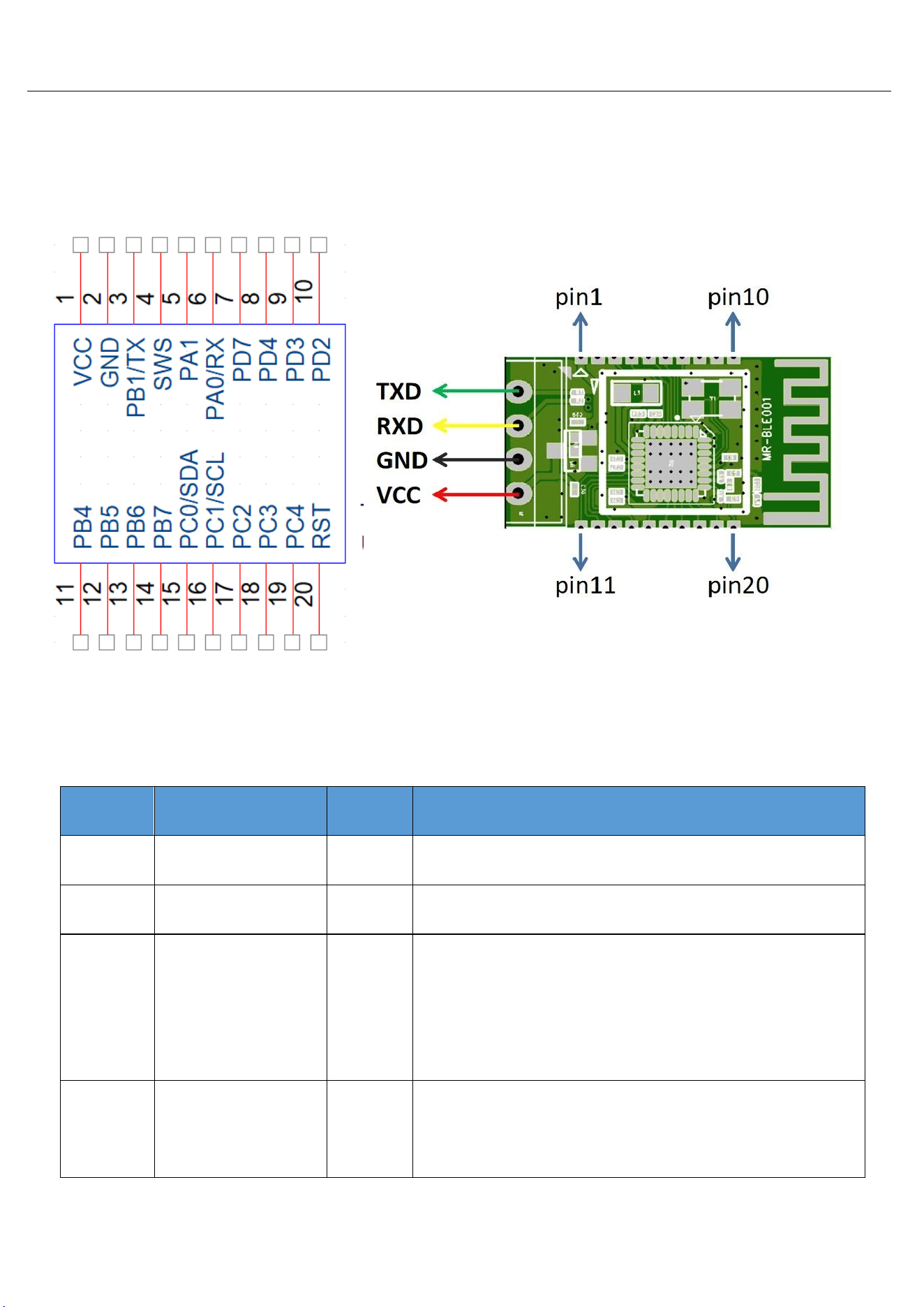
3. Foot Decription
█Interface decription
Pin # Name Type Description
1 VCC PWR 3.3V Powered
2 GND PWR ground pin
3 PB1_UTX I/O
PWM4 output / UART_TX / Antenna
select pin 2 / Low power comparator
input / SAR ADC input / GPIO PB[1]
4 SWS I/O Single wire slave/ UART_RTS / GPIO
PA[7]

———————————————————————————————————————————————————————————————————
5 PA1 I/O
DMIC clock / UART 7816 clock / I2S
clock /
GPIO PA[1]
6 PA0_URX I/O
DMIC data input / PWM0 inverting
output / UART_RX / GPIO PA[0]
7 PD7 I/O
SPI clock (I2C_SCK) / I2S bit clock /
UART 7816 TRX (UART_TX) / GPIO
PD[7]
8 PD4 I/O
Single wire master / I2S serial data
output / PWM2 inverting output /
GPIO PD[4]
9 PD3 I/O
PWM1 inverting output / I2S serial data
input / UART 7816 TRX (UART_TX) /
GPIO PD[3]
10 PD2 I/O
SPI chip select (Active low) / I2S left
right channel
select / PWM3 output / GPIO PD[2]
11 PB4 I/O
SDM positive output 0 / PWM4 output
/
Low power comparator input /
SAR ADC input / GPIO PB[4]

———————————————————————————————————————————————————————————————————
12 PB5 I/O
SDM negative output 0 / PWM5 output
/
Low power comparator input /
SAR ADC input / GPIO PB[5]
13 PB6 I/O
SDM positive output 1 / SPI data input
(I2C_SDA) / UART_RTS / Low power
comparator input /
SAR ADC input / GPIO PB[6]
14 PB7 I/O
SDM negative output 1 / SPI data
output / UART_RX / Low power
comparator input /
SAR ADC input / GPIO PB[7]
15 PC0_SDA I/O
I2C serial data / PWM4 inverting
output / UART_RTS / PGA left channel
positive input / GPIO PC[0]
16 PC1_SCL I/O
I2C serial clock / PWM1 inverting
output / PWM0
output / PGA left channel negative
input /
GPIO PC[1]
17 PC2 I/O PWM0 output / UART 7816 TRX
———————————————————————————————————————————————————————————————————
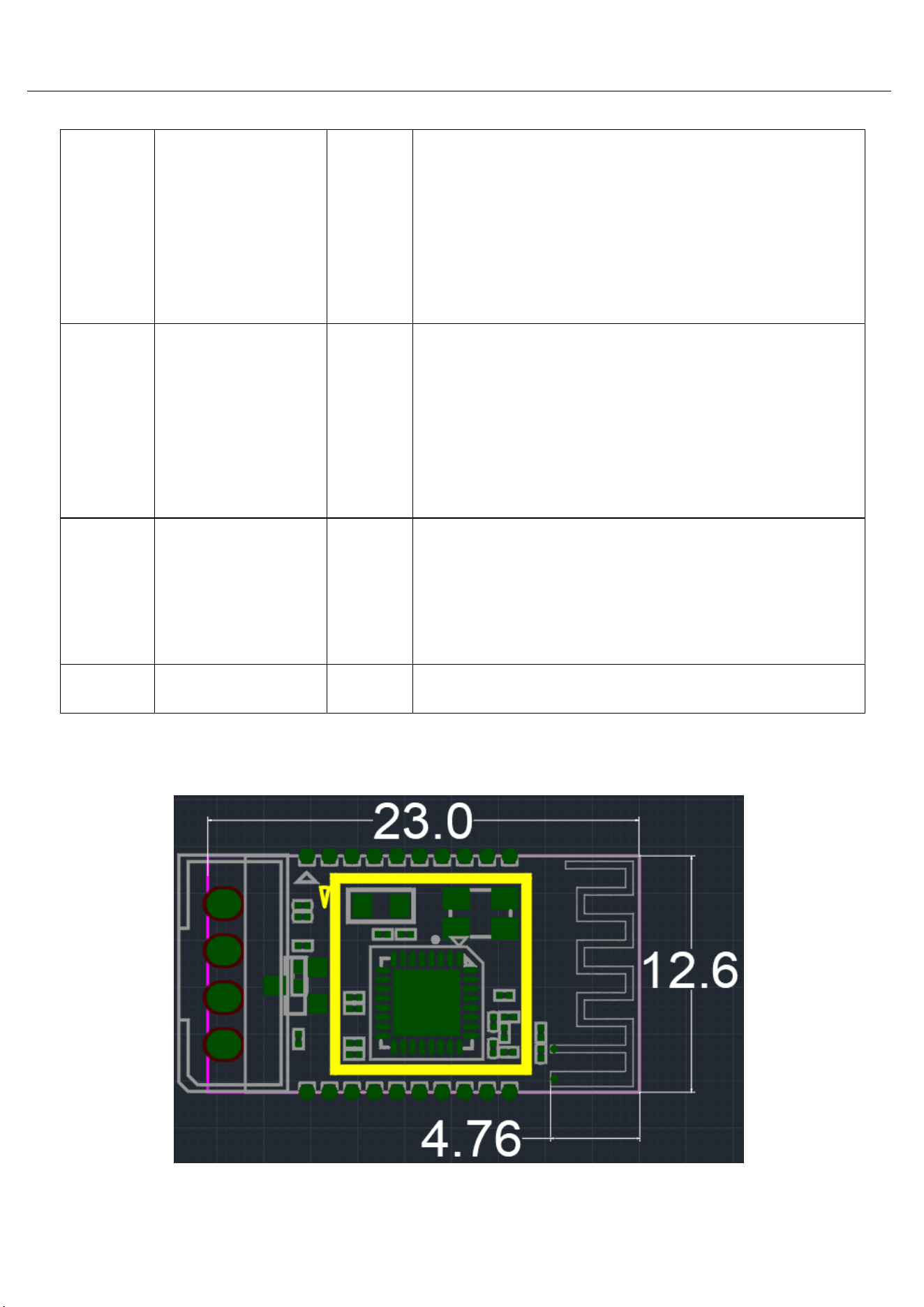
4. Module Measurement
(UART_TX) /
I2Cserial data / (optional) 32kHz crystal
output / PGAright channel positive
input / GPIO PC[2]
18 PC3 I/O
PWM1 output / UART_RX / I2C serial
clock / (optional)32kHz crystal input /
PGA right channel negative input /
GPIO PC[3]
19 PC4 I/O
PWM2 output / UART_CTS / PWM0
inverting output / SAR ADC input /
GPIO PC[4]
20 RST RESET Power on reset, active low
———————————————————————————————————————————————————————————————————
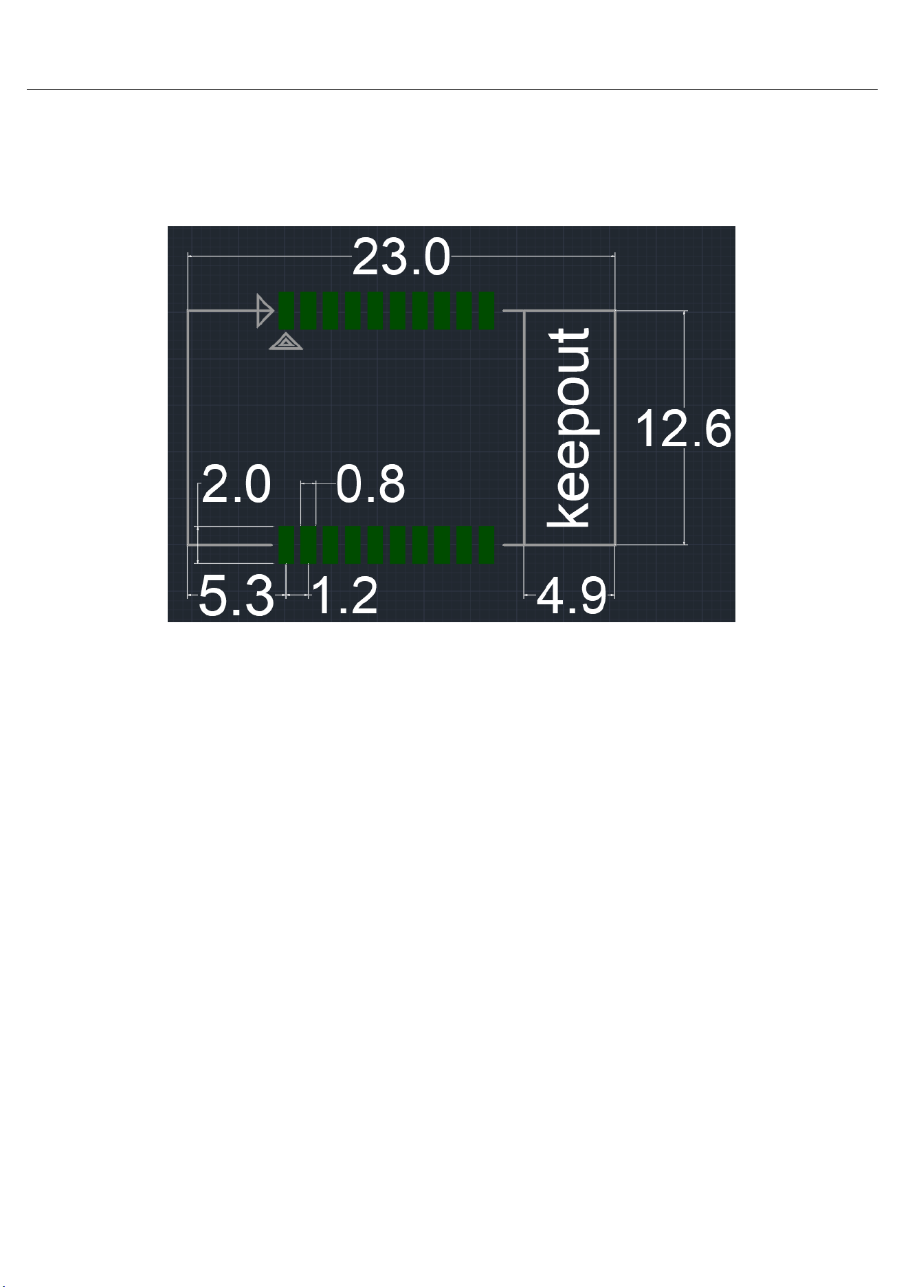
5. Reference PCB Package
The Bluetooth operating frequency is 2.4GHz, and the influence of various
factors on wireless transceiver should be avoided as much as possible.
Notice: ▶ Avoid using metal for the part of the product housing that
▶ The metal screws inside the product should be kept away from the RF part
of the module.
———————————————————————————————————————————————————————————————————
▶ To maximize RF performance, user board layout should follow the
following recommendations: 1) Antenna clearance area: the user board
located directly under the antenna area of the module cannot have any
copper foil (including power, ground, signal layers). 2) Module location:
Ideally, the module should be arranged in a corner of the user's mainboard,
and the PCB antenna is located at the far end of the mainboard. This position
minimizes the antenna clearance area
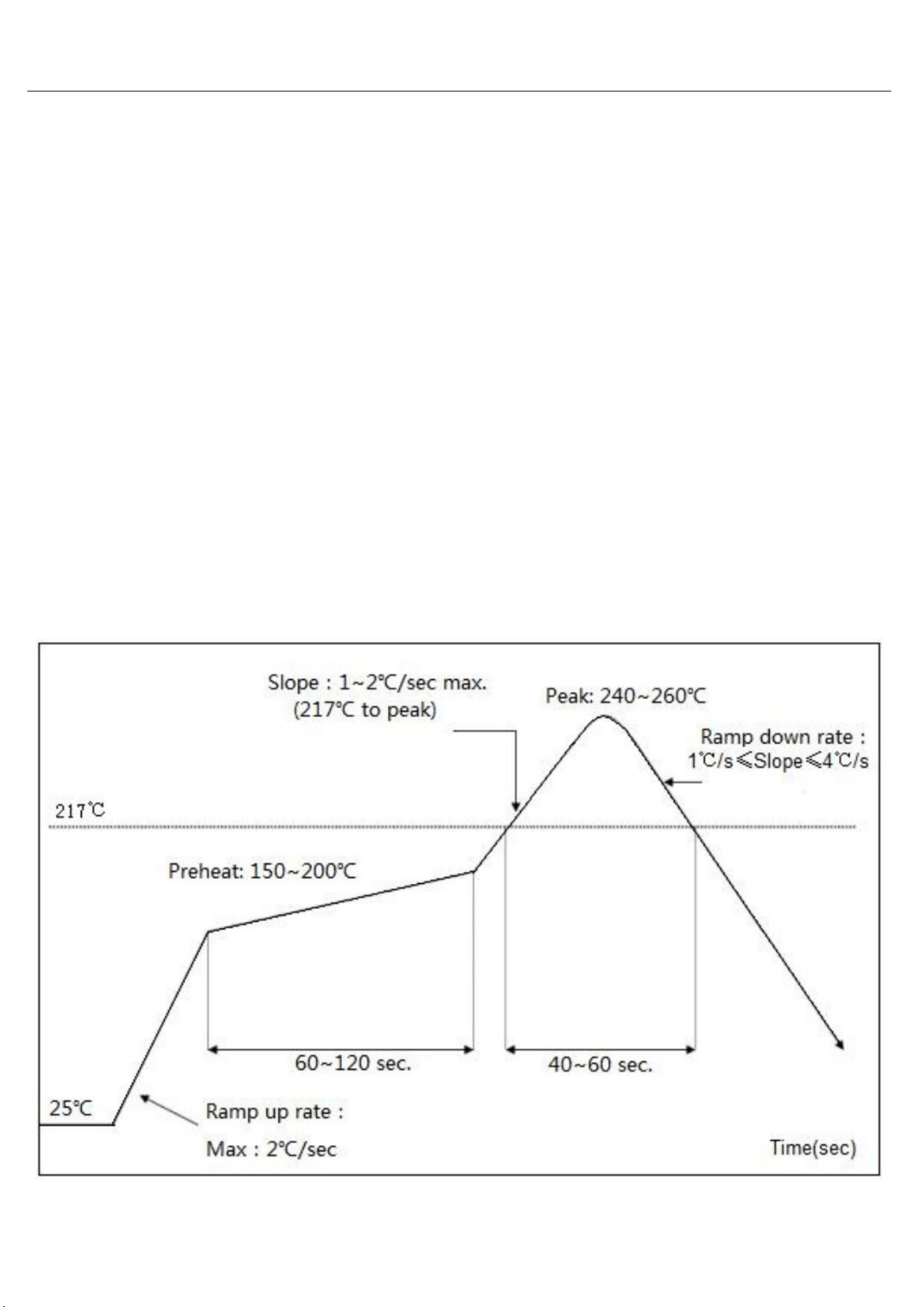
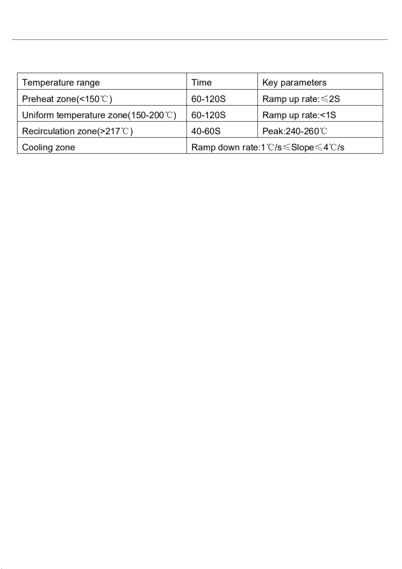
6. Furnace parameters
█Refer to the following settings for the furnace parameters:
FCC Statement
Any Changes or modifications not expressly approved by the party responsible for compliance
could void the user’s authority to operate the equipment.
This device complies with part 15 of the FCC Rules. Operation is subject to the following two
conditions:
(1)This device may not cause harmful interference, and
(2)This device must accept any interference received, including interference that may cause
undesired operation.
FCC Radiation Exposure Statement:
This equipment complies with FCC radiation exposure limits set forth for an uncontrolled
environment .This equipment should be installed and operated with minimum distance 20cm
between the radiator& your body. This transmitter must not be located or operating in
conjunction with any other antenna or transmitter.
Note : This equipment has been tested and found to comply with the limits for a Class B digital
device, pursuant to part 15 of the FCC Rules. These limits are designed to provide reasonable
protection against harmful interference in a residential installation. This equipment
generates,uses and can radiate radio frequency energy and, if not installed and used in
accordance with the instructions, may cause harmful interference to radio communications.
However, there is no guarantee that interference will not occur in a particular installation. If this
equipment does cause harmful interference to radio or television reception, which can be
determined by turning the equipment off and on, the user is encouraged to try to correct the
interference by one or more of the following measures:
—Reorient or relocate the receiving antenna.
—Increase the separation between the equipment and receiver.
—Connect the equipment into an outlet on a circuit different from that to which the receiver is
connected.
—Consult the dealer or an experienced radio/TV technician for help.
———————————————————————————————————————————————————————————————————