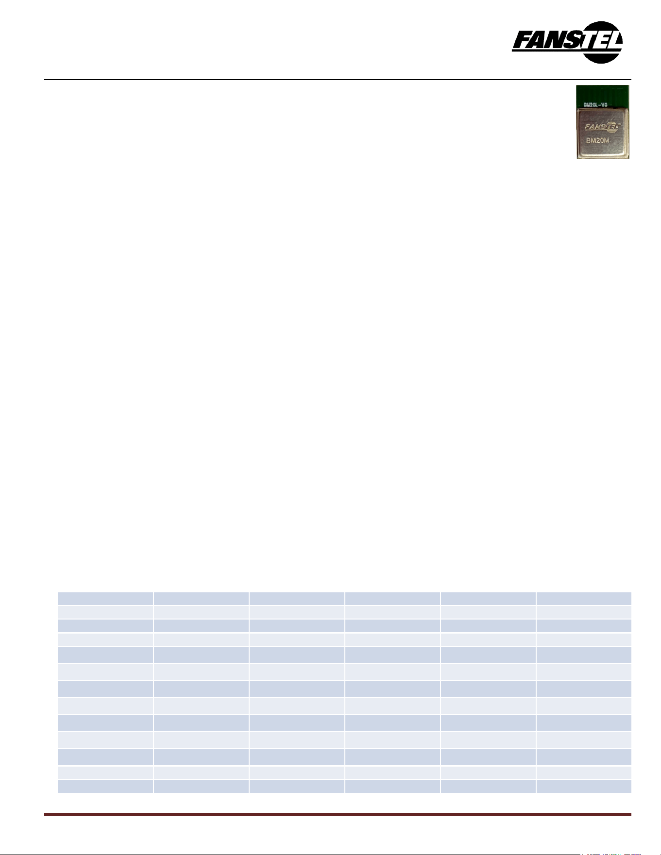
Bluetooth 6.0, 802.15.4 Module BM20C Draft Ver 0.81 June 2026
1
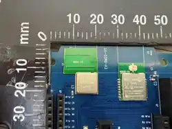
BM20C is a powerful, highly flexible, ultra low power Bluetooth Low Energy (BLE) using Nordic
nRF54LM20A SoC. With a ARM
Cortex
TM
M33 MCU at 128 MHz, a RISC-V co-processor for peripherals,
embedded 2.4GHz multi-protocol transceiver, and an integrated PCB trace, chip antenna or connection for
an external antenna. The nRF54LM20B variant includes an Axon Neural Processing Unit (NPU) - an edge
AI accelerator.
BM20C footprint is compatible with (1) BM20NE, a module with Nordic nRF21540 power amplifier; (2)
BM20XE, a module with Skyworks SKY66403 power amplifier; (3) WM02C20C, a combo module with
nRF7002 WiFi 6. All modules can be with or without Axon NPU.
BM20C uses an nRF54LM20A SoC. The corresponding module with an nRF54LM20B is BM20BC.
Specifications:
BLE 6.0, IEEE 802.15.4-2020 Transceiver
• Complete RF solution with integrated antenna
• BLE: 2Mbps, 1Mbps, 500kbps, 125kbps.
• IEEE 802.15.4-2020: 250 kbps.
• Proprietary: 4Mbps, 2Mbps, 1Mbps.
• 128-bit AES/ECB/CCM/AAR coprocessor.
• Programmable TX power, from -10 dBm to +8 dBm, in 1
dB step.
Platform Security
• Secure/non-secure memory protection
• Symmetric and asymmetric key crypto accelerator.
• Secure key management.
• Tamper detection.
• Immutable boot partition.
• Debug access port protection.
• Individual watchdog timers for secure and non-secure
context.
Application processor
• ARM
R
Cortex
R
M33 with TrustZone
R
, 128MHz.
• 500 EEMBC CoreMark score running from non-volatile
memory, 3.90 CoreMark per MHz.
• 2036 KB non-volatile memory(RRAM), 512 KB RAM.
• Floating point unit, DSP instructions.
• Data watchpoint and trace.
• Serial Wire Debug (SWD)
Peripherals
• RISC-V Coprocessor.
• High-speed USB (480 Mbps), Full speed (12 Mbps),
and low speed (1.5 Mbps)
• A global real-time counter can run is System OFF
mode.
• Seven 32 bit timers with counter mode.
• Six fully featured serial interfaces with EasyDMA,
supporting I
2
C, SPI controller/peripheral, and UART.
• One high speed capable SPIM (32 MHz) or UART with
EasyDMA.
•
Three PWM units with EasyDMA.
• Time Division Multiplexed (TDM) sound interface.
• Two pulse density modulated (PDM) microphone
interface, 48x, 50x, 64x, 80x, 96x, 150x, and 192x
decimation ratios.
• ADC with up to 8 programmable gain channels. 14-bit at
31.25 ksps, 12 bit at 250 ksps, and up to 10 bit at 2
maps.
• NFC.
• 2 x QDEC.
• 90 LGA pins, 66 GPIOs.
• 32.0 MHz and 32.768 kHz crystals embedded.
• 1.8V and 3.3V supply voltage.
• All evaluation boards use an nRF54LM20B module.
Don’t use the Axon NPU if an nRF54LM20A module is
used.
• Operation temperature: - 40°C to + 125°C
Model Summaries
module
BM20M/BM20BM
BM20C/BM20BC
BM20E/BM20BE
BM20F/BM20BF
BM20P/BM20BP
SoC
nRF54LM20A/B
nRF54LM20A/B
nRF54LM20A/B
nRF54LM20A/B
nRF54LM20A/B
Size, mm
10.0x14.0mm
10.0x14.8mm
10.0x15.0 mm
10(15.2) x 20.8
10.0 x 10.5
Antenna
PCB Trace
Chip
U.FL for external
High perf. PCB
Pads for external
BLE range
300M est.
500M, est.
FCC ID
ISED ID
CE, RCM
TELEC
NCC
KCC
Evaluation board
EV-BM20BM
EV-BM20BC
EV-BM20BE
EV-BM20BF
EV-BM20BP
Availability
Sample/NonStock
Sample/Sample
Sample/NonStock
NonStock/Sample Q3
NonStock/Samples Q3

Bluetooth 6.0, 802.15.4 Module BM20C Draft Ver 0.81 June 2026
2
Of Contents
1. Introduction ....................................................................................................................................................... 3
BM20C Block Diagram ...................................................................................................................................... 3
BM20M .............................................................................................................................................................. 4
BM20C and BM20BC ........................................................................................................................................ 4
BM20E .............................................................................................................................................................. 4
BM20BF ............................................................................................................................................................ 4
BM20BP ............................................................................................................................................................ 4
2. BM20C Specifications ....................................................................................................................................... 5
Nordic SoCs ...................................................................................................................................................... 5
Mechanical Drawings ........................................................................................................................................ 6
BM20C pin map .............................................................................................................................................. 11
PIN Function BM15C, BM20C, BMH20C ........................................................................................................ 12
Upgrading to BM20NE, BM20XE, WM02C20C .............................................................................................. 15
Mounting BM20C on the Host PCB ................................................................................................................ 18
Suggestion for Battery Power Application ....................................................................................................... 18
EV-BM20BC Evaluation Board Schematics .................................................................................................... 19
Evaluation Board ............................................................................................................................................. 21
3. Firmware Development ................................................................................................................................... 22
Loading Firmware into Evaluation Board Through a Nordic DK ..................................................................... 22
Procedures to Load Firmware ......................................................................................................................... 23
Preloaded Firmware ........................................................................................................................................ 26
4. Miscellaneous ................................................................................................................................................. 27
Soldering Temperature-Time Profile for Re-Flow Soldering ........................................................................... 27
Cautions, Design Notes, and Installation Notes .............................................................................................. 27
Packaging ....................................................................................................................................................... 30
FCC Label ....................................................................................................................................................... 30
5. Revision History .............................................................................................................................................. 31
6. Contact Us ....................................................................................................................... 錯誤! 尚未定義書籤。
Bluetooth 6.0, 802.15.4 Module BM20C Draft Ver 0.81 June 2026
3
1. Introduction
BM20C is a powerful, highly flexible, ultra low power Bluetooth Low Energy (BLE) using Nordic nRF54LM20
SoC. With an ARM
Cortex
TM
M33 MCU at 128 MHz, a RISC-V MCU for peripherals, embedded 2.4GHz multi-
protocol transceiver, and an integrated PCB trace or chip antenna or u.FL connector for an external antenna. It
allows faster time to market with reduced development cost.
The following modules use nRF54LM20A or nRF54LM20B SoC and have compatible footprints. BM20C is the
core of these series of modules.
• BM20C, BM20BC, BM20E, BM20BF, BM20M, BM20BP are referred as BM20C in this product specifications.
• Modules with a Nordic nRF21540 power amplifier, BM20NE.
• Modules with a Skyworks SKY66403 power amplifier, BM20XE.
• Modules with a Nordic nRF7002 WiFi 6 SoC, WM02C20C.
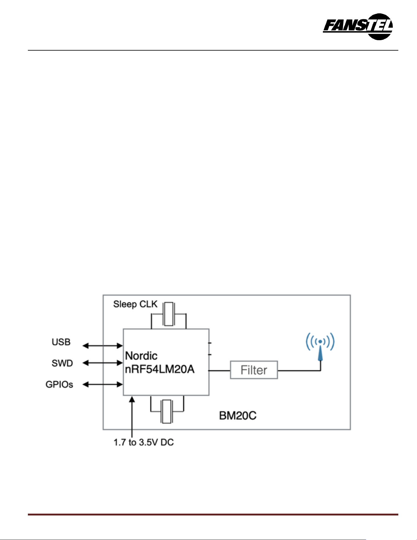
The following is a block diagram of BM20C. Antenna circuit and main clock are integrated. All 66 GPIOs of
nRF54LM20A can be accessed from main board. For lower power consumption at idle state, a 32.768 kHz
crystal is embedded. Connection to an external NFC (Near Field Communication) antenna is provided.
BM20C Block Diagram

Bluetooth 6.0, 802.15.4 Module BM20C Draft Ver 0.81 June 2026
4
BM20C Series modules have the same features except the followings.
BM20M
• BM20M has an nRF54LM20A SoC.
• Integrated PCB trace antenna
• Size: 10x14.0 mm
• BM20BM has an nRF54LM20B SoC to support edge AI applications.
• BM20BM is manufactured to order only.
BM20C and BM20BC
• BM20C has an nRF54LM20A SoC.
• Integrated high performance chip antenna
• Size: 10x14.8mm
• BM20BC has and nRF54LM20B SoC to support edge AI applications.
BM20E
• BM20E has an nRF54LM20A SoC.
• An u.FL connector for external antenna
• Size: 10x15.0mm.
• BM20BE has an nRF54LM20B SoC to support edge AI applications.
• BM20BE is manufactured to order only.
BM20BF
• BM20BF has an nRF54LM20B SoC to support edge AI applications.
• Integrated high performance PCB trace antenna
• Size: 10.0(15.2 in antenna area)x20.8 mm
• BM20F has an nRF54LM20A SoC.
• BM20F is manufactured to order only.
BM20BP
• BM20BP has an nRF54LM20B SoC to support edge AI applications.
• Pads for external antenna connection.
• Size: 10.0x10.5mm.
• BM20P has an nRF54LM20A.
• BM20P is manufactured to order only.
Bluetooth 6.0, 802.15.4 Module BM20C Draft Ver 0.81 June 2026
5
2. BM20C Specifications
Nordic SoCs
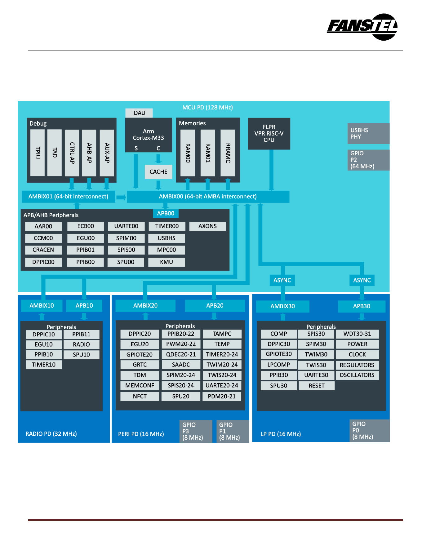
A block diagram of nRF54LM20B is below. The AXONS block is removed in nRF54LM20A.
Bluetooth 6.0, 802.15.4 Module BM20C Draft Ver 0.81 June 2026
6
Mechanical Drawings
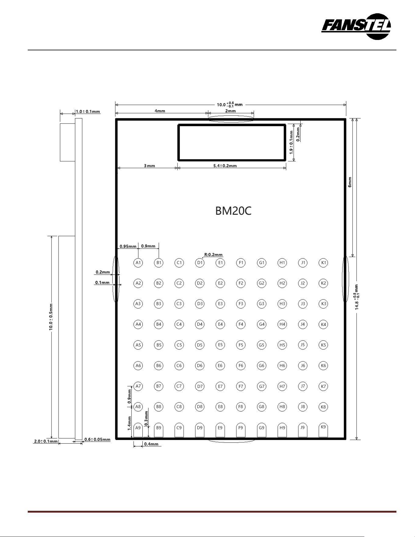
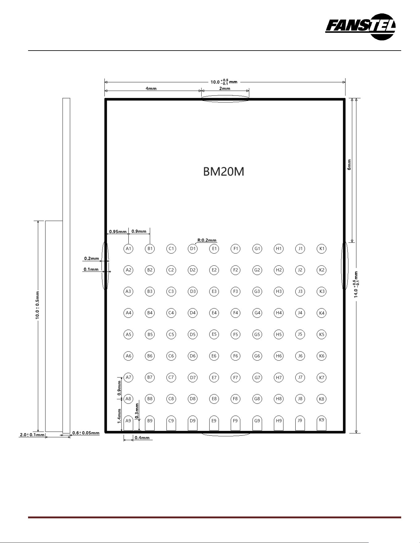
The following is mechanical drawings of BM20C and BM20BC, top view.
Bluetooth 6.0, 802.15.4 Module BM20C Draft Ver 0.81 June 2026
7
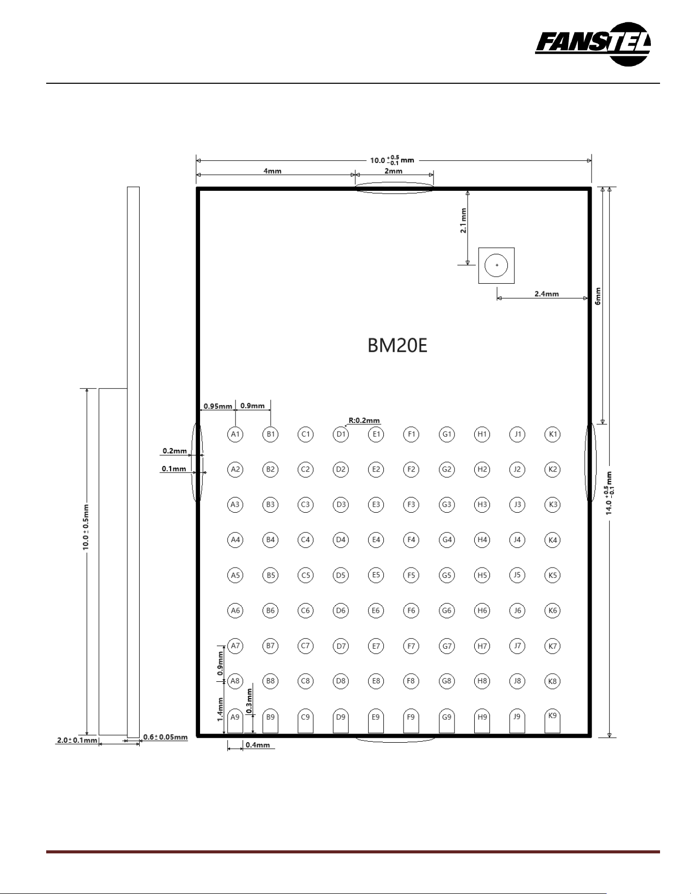
The following is mechanical drawings of BM20M and BM20BM, top view.
Bluetooth 6.0, 802.15.4 Module BM20C Draft Ver 0.81 June 2026
8
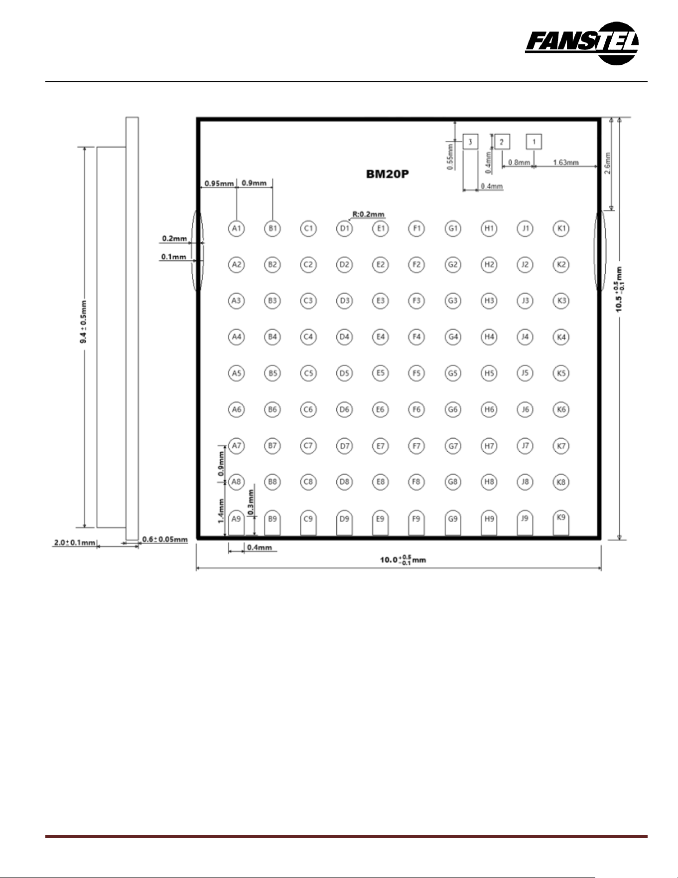
The following is mechanical drawings of BM20E and BM20BE, top view.
Bluetooth 6.0, 802.15.4 Module BM20C Draft Ver 0.81 June 2026
9
Bluetooth 6.0, 802.15.4 Module BM20C Draft Ver 0.81 June 2026
10
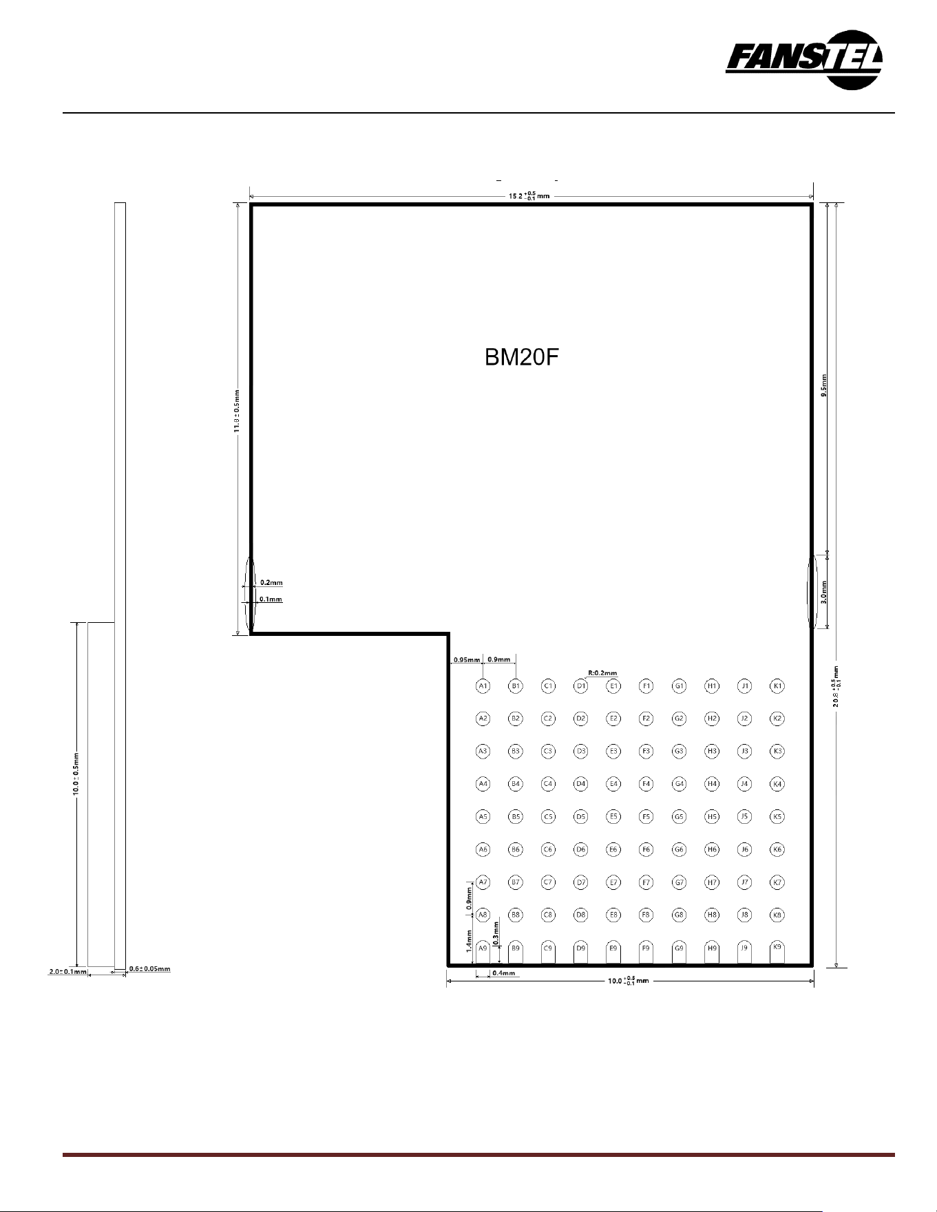
The following is mechanical drawings of BM20F and BM20BF, top view.
Bluetooth 6.0, 802.15.4 Module BM20C Draft Ver 0.81 June 2026
11
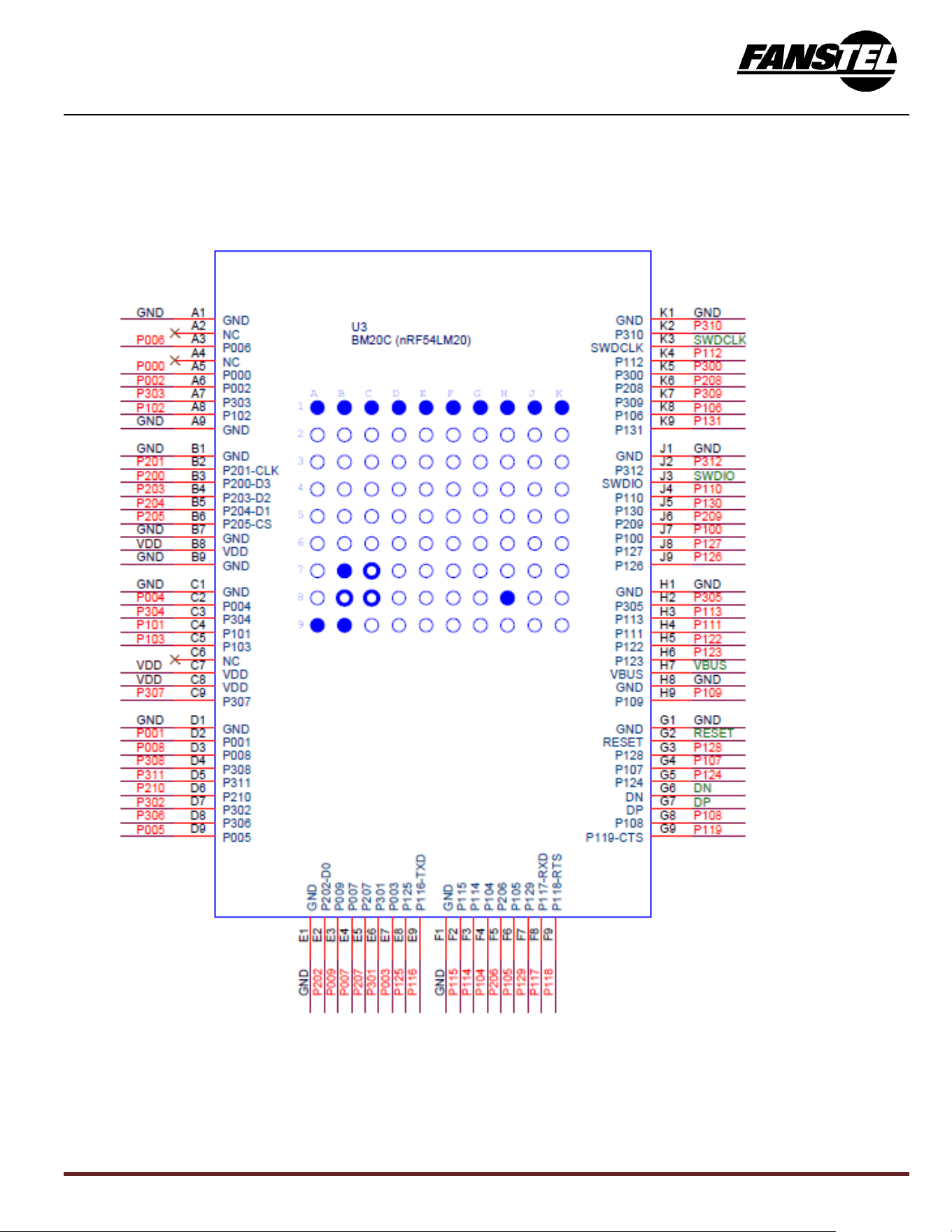
BM20C pin map
BM20C is an nRF54LM20A module with 64 GPIO pins. All GPIO pins are accessible.
Bluetooth 6.0, 802.15.4 Module BM20C Draft Ver 0.81 June 2026
12
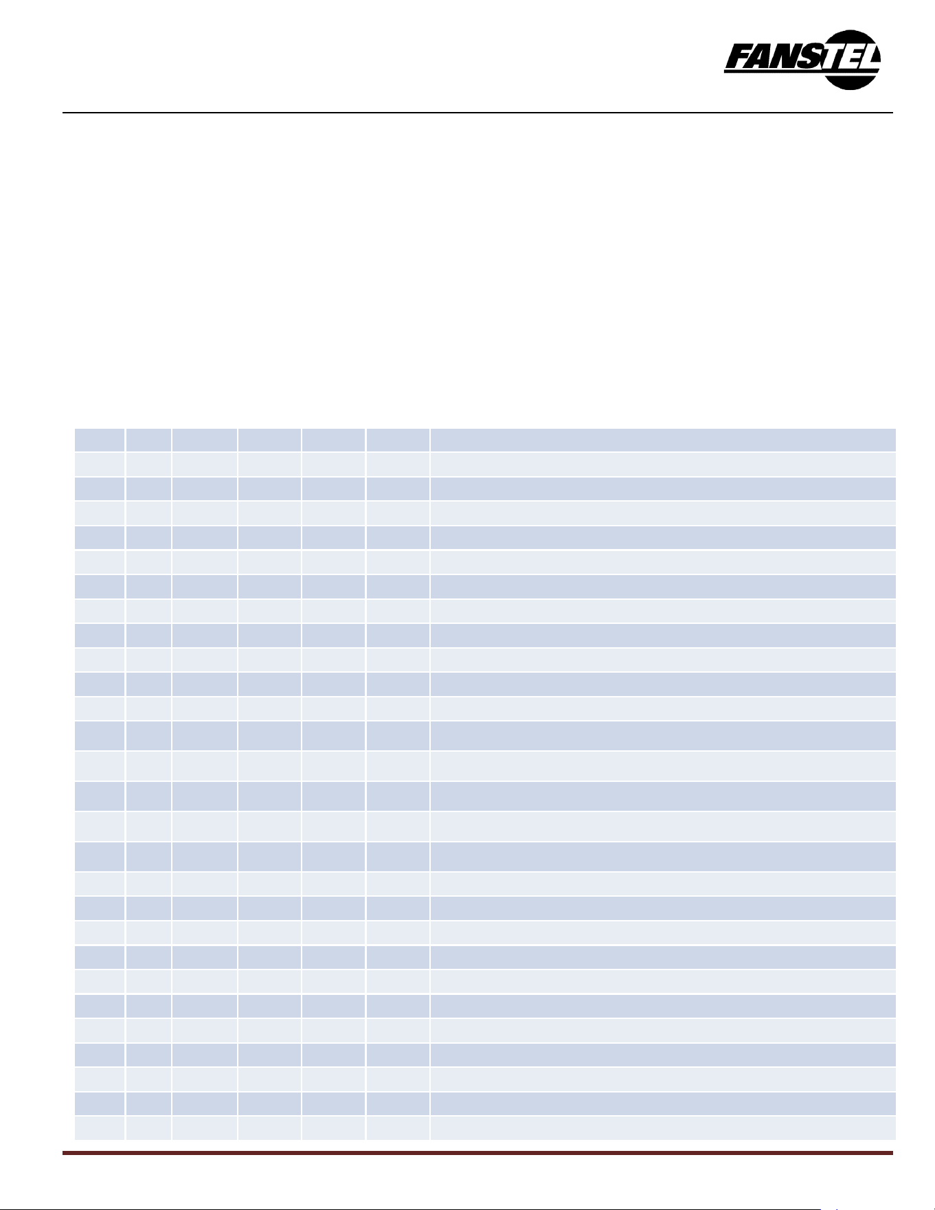
PIN Function BM15C, BM20C, BMH20C
In this section, the following abbreviations are used.
• BM15, an nRF54L15 Bluetooth module representing BM15M, BM15C, BM15E.
• BM20, an nRF54LM20A or nRF54LM20B Bluetooth module representing BM20C, BM20BC, BM20E,
BM20BF, BM20M, BM20BP, BM20NE, BM20XE, BM20BNE, BM20BXE.
• BMH20, an nRF54H20 Bluetooth module representing BMH20C, BMH20E, BMH20XE.
• L15, nRF54L15.
• L20, nRF54LM20A or nRF54LM20B.
• H20, nRF54H20.
UART pins of BM15 in EV-BM15 are different from UART pins of BM15 in the EV-BM20 design to
accommodate BM15, BM20, and BMH20. Different firmware configuration is required.
BMH20C and BM20C are only partially footprint compatible. The power supply voltages are different. The
GPIO pin functions are also different.
Module
L15
BM15
L20
BM20
H20
BMH20
pin#
pin#
Name
Name
pin#
Name
Descriptions
A1
GND
GND
GND
Ground
A2
No Connect
A3
37
P109
H2
P006
C6
P111
GPIO
A4
A12
VDD-P9
VDD-P9, DC to set operating voltage of port 9. 1.8V or 3.3V.
A5
K3
P000
L12
P601
BM20, GPIO; BMH20, QSPI CKN.
A6
J3
P002
M11
P602
BM20, GPIO; BMH20, QSPI RWDS
A7
H4
P303
L11
P604
BM20, GPIO; BMH20, QSPI D7.
A8
J7
P102
L10
P606
BM20, GPIO; BMH20, QSP D6
A9
GND
GND
GND
Ground
B1
GND
GND
GND
Ground
B2
38
P110
C10
P201-
CLK
M12
P600
GPIO; BM20, BMH20 QSPI Clock
B3
39
P111
B10
P200-
D3
M8
P609
GPIO, BM15,Analog input AIN4; BM20, BMH20, QSPI D3;
B4
40
P112
E10
P203-
D2
L8
P610
GPIO, BM15,Analog input AIN5; BM20, BMH20, QSPI D2;
B5
41
P113
F10
P204-
D1
M10
P605
GPIO, BM15,Analog input AIN6, UART TXD in EV-BM15C; BM20, BMH20, QSPI
D1
B6
42
P114
G9
P205-
CS
K12
P603
GPIO, BM15,Analog input AIN7, UART RXD in EV-BM15C; BM20, BMH20, QSPI
CS;
B7
49
GND
GND
GND
Ground
B8
36
VDD
A3
VDD
L4
VDD
BM15, 1.7V to 3.6V; BM20, 1.7V to 3.5V; BMH20, 1.71 to 1.98V.
B9
49
GND
GND
GND
Ground
C1
GND
GND
BM15,NC; BM20, ground;
C2
J1
P004
L9
P608
BM20, GPIO; BMH20, QSPI D5
C3
J4
P304
M7
P611
BM20, GPIO; BMH20, QSPI D4
C4
J6
P101
L7
P612
BM20, GPIO; BMH20, RESET.
C5
H9
P103
K7
P613
BM20, GPIO; BMH20, CS1_CSN
Bluetooth 6.0, 802.15.4 Module BM20C Draft Ver 0.81 June 2026
13
C6
NC
L1
VDDH
BMH20, High voltage power supply, 2.05V to 5.5V.
C7
VDD
A12
VDD
BM20, 1.7 to 3.5V; BMH20, DC power supply 1.71 to 1.98V
C8
48
VDDM
A3
VDD
L4
VDD
BM15, 1.8V to 3.6V; BM20, 1.7V to 3.5V; BMH20, 1.71 to 1.98V.
C9
2
P101
G5
P307
C9
P000
BM15, GPIO, connection for 32.768 kHz crystal; BM20, BMH20, GPIO;
D1
GND
GND
GND
Ground
D2
K2
P001
D11
P001
BM20, BMH20, GPIO.
D3
F3
P008
D10
P002
BM20, BMH20, GPIO.
D4
G4
P308
C10
P905
BM20, BMH20, GPIO
D5
E4
P311
C11
P904
BM20, BMH20, GPIO
D6
F9
P210
B10
P903
BM20, BMH20, GPIO
D7
H5
P302
B11
P902
BM20, BMH20, GPIO.
D8
1
P100
G6
P306
A10
P901
GPIO, BM15, connection for 32.768 kHz crystal
D9
3
P102
H3
P005
K11
P900
GPIO, BM15, NFC pin.
E1
GND
GND
GND
Ground
E2
D10
P202-
D0
M9
P607-D0
BM20, BMH20, QSPI D0;
E3
E3
P009
D9
P003
BM20, GPIO
E4
G3
P007
D8
P004
BM20, GPIO
E5
C9
P207
E11
P005
BM20, GPIO
E6
H6
P301
E10
P006
BM20, GPIO
E7
J2
P003
E9
P007
BM20, GPIO
E8
4
P103
E7
P125
F11
P008
BM15, GPIO, NFC pin; BM20, BMH20, GPIO;
E9
5
P104
B3
P116-
TXD
J2
P206-
TXD
BM15, analog input AIN0, configurable as UART TXD; BM20,BMH20, UART
TXD.
F1
GND
GND
GND
Ground
F2
B2
P115
F10
P009
BM20, GPIO;
F3
C2
P114
E4
P102
BM20, GPIO; BMH20, IRQ
F4
J9
P104
B4
P100
BM20, GPIO; BMH20, BUCK-EN
F5
B9
P206
F9
P010
BM20, GPIO;
F6
H8
P105
A6
P109
BM20, GPIO; BMH20, VDDIO_EN
F7
H10
P129
G9
P011
BM20, GPIO;
F8
6
P105
B4
P117-
RXD
H2
P204-
RXD
BM15,Analog input AIN1, configurable as UART RXD; BM20,BMH20, UART
RXD.
F9
7
P106
B5
P118-
RTS
K3
P207-
RTS
BM15,Analog input AIN2, configurable as UART RTS; BM20, BMH20 UART
RTS.
G1
GND
GND
BM15, NC; BM20, BMH20, ground;
G2
30
/Reset
F2
/Reset
L7
/Reset
/Reset, active low.
G3
D8
P128
J11
P706
BM20,BMH20, GPIO
G4
G8
P107
B5
P106
BM20, BMH20, SPI_MISO;
G5
D7
P124
J9
P707
BM20, BMH20 GPIO.
G6
K4
DN
B8
DN
BM20, USB port Data
G7
K5
DP
B7
DP
BM20, USB port Data
G8
9
P108
F8
P108
A5
P107
BM15, BM20, GPIO; BMH20, SPI_Status0
G9
8
P107
B6
P119-
CTS
J3
P205-
CTS
BM15, GPIO, Analog input AIN3, configurable as UART CTS; BM20, BMH20
UART CTS;
Bluetooth 6.0, 802.15.4 Module BM20C Draft Ver 0.81 June 2026
14
H1
GND
GND
BM15,NC; BM20, ground;
H2
29
P004
G7
P305
H10
P703
GPIO.
H3
C3
P113
B6
P110
BM20,BMH20, GPIO, Status1;
H4
C5
P111
D4
P101
BM20, GPIO; BMH20, SPI-CLK
H5
D6
P122
H9
P704
BM20, GPIO;
H6
B7
P123
J11
P705
BM20, GPIO;
H7
K7
VBUS
A9
VBUS
BM20, BMH20, USB power supply, 5V nominal, 4.4V to 5.5V.
H8
49
GND
GND
GND
Ground
H9
11
P200
E8
P109
D6
P108
BM15, GPIO; BM20, GPIO, REQ; BMH20, REQ
J1
GND
GND
BM15,NC; BM20,BMH20, ground.
J2
28
P003
D4
P312
K1
P209
GPIO
J3
25
SWDIO
G2
SWDIO
G12
SWDIO
Serial Wire Debug data.
J4
23
P000
D5
P110
D5
P104
GPIO; BMH20, SPI_SS.
J5
20
P209
J10
P130
H1
P210
GPIO; BM20, BMH20, NFC_N
J6
18
P207
E9
P209
J1
P211
GPIO; BM20, BMH20, NFC_P
J7
14
P203
K8
P100
G11
P700
GPIO; BM20, BMH20, GPIO.
J8
13
P202
C8
P127
G10
P701
GPIO; BM20, BMH20, GPIO.
J9
12
P201
B8
P126
H11
P702
GPIO; BM20, BMH20, GPIO.
K1
GND
GND
BM15, NC; BM20, BMH20, Ground.
K2
27
P002
F4
P310
F3
P200
GPIO
K3
26
SWDC
LK
G1
SWDCL
K
F12
SWDCLK
Serial Wire Debug clock
K4
24
P001
C4
P112
E5
P103
GPIO; BMH20, SPI_GRANT
K5
21
P210
H7
P300
G3
P201
GPIO;
K6
19
P208
D9
P208
G2
P202
GPIO;
K7
17
P206
F7
P309
H3
P203
GPIO;
K8
16
P205
J8
P106
C5
P105
GPIO; BM20, BMH20, GPIO, SPI_MOSI.
K9
15
P204
K9
P131
K2
P208
GPIO; BM20, BMH20, GPIO.
Bluetooth 6.0, 802.15.4 Module BM20C Draft Ver 0.81 June 2026
15
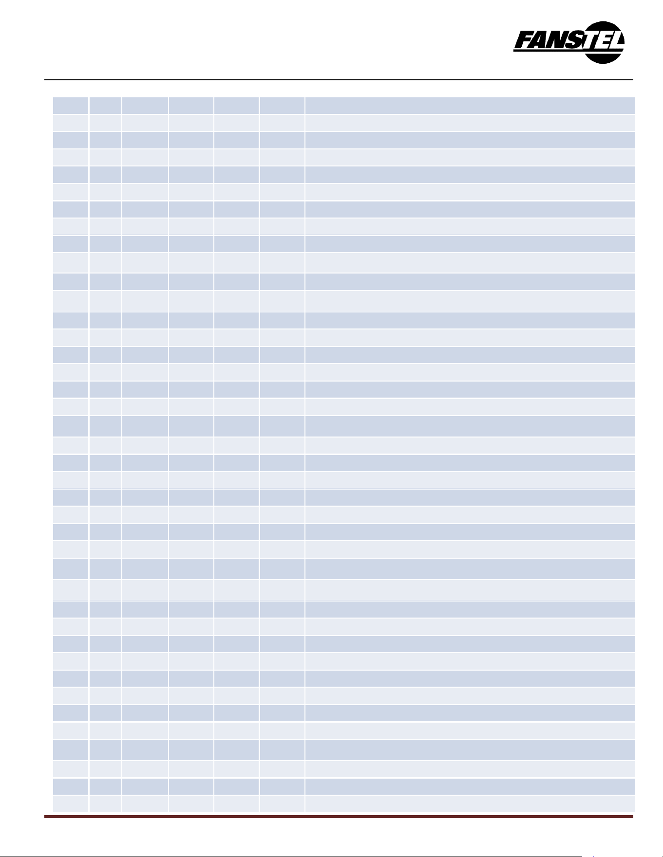
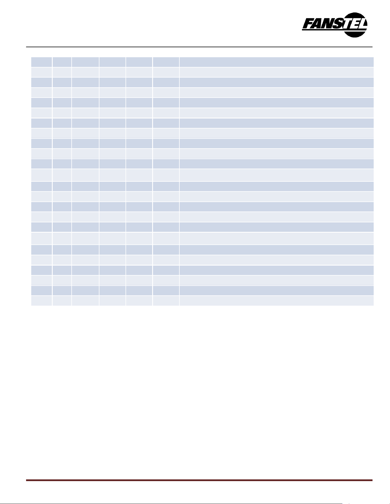
Upgrading to BM20NE, BM20XE, WM02C20C
In this section, the following abbreviations are used.
• BM20, an nRF54LM20A or nRF54LM20B Bluetooth module representing BM20C, BM20E, BM20M, BM20P.
• 20NE, an nRF54LM20A/B + nRF21540 PA Bluetooth module representing BM20NE and BM20BNE
(nRF54LM20B).
• 20XE, an nRF54LM20A/B + SKY66403 PA Bluetooth module representing BM20XE and BM20BXE
(nRF54LM20B).
• WM20, nRF54LM20A/B and nRF7002 WiFi 6 combo module.
• L20, nRF54LM20A or nRF54LM20B.
• 7002, nRF7002 WiFi 6 SoC.
Module
L20
BM20
20NE
20XE
WM20
pin#
Name
Name
Name
Name
Descriptions
A1
GND
GND
GND
Ground
A2
VDD-PA
VDD-PA
3.3V DC supply for power amplifier.
A3
H2
P006
P006
P006
P006
GPIO
A4
A5
K3
P000
P000
P000
P000
BM20, GPIO
A6
J3
P002
P002
P002
P002
BM20, GPIO
A7
H4
P303
NC
P303
P303
BM20, GPIO; 20NE, SCK.
A8
J7
P102
NC
NC
P102
BM20, WM20, GPIO; 20XE, NC, internal PA control nCTX; 20NE, TX-EN.
A9
GND
GND
GND
GND
Ground
B1
GND
GND
GND
GND
Ground
B2
C10
P201-
CLK
P201-
CLK
P201-
CLK
P201-
CLK
GPIO, QSPI CLK
B3
B10
P200-D3
P200-D3
P200-D3
P200-D3
GPIO, QSPI D3;
B4
E10
P203-D2
P203-D2
P203-D2
P203-D2
GPIO, QSPI D2;
B5
F10
P204-D1
P204-D1
P204-D1
P204-D1
GPIO, QSPI D1
B6
G9
P205-CS
P205-
CS
P205-
CS
P205-
CS
GPIO, QSPI CS;
B7
GND
GND
GND
GND
Ground
B8
A3
VDD
VDD
VDD
VDD
DC power supply 1.7V to 3.5V
B9
GND
GND
GND
GND
Ground
C1
GND
GND
GND
GND
BM15,NC; BM20, ground;
C2
J1
P004
P004
P004
P004
GPIO;
C3
J4
P304
P304
P304
P304
GPIO;
C4
J6
P101
NC
NC
P101
BM20, WM20, GPIO; 20XE, NC, internal PA control, nCHL; 20NE, MODE.
C5
H9
P103
NC
NC
P103
BM20, WM02, GPIO; 20XE, NC, internal PA control, nANT-SEL; 20NE, ANT-SEL.
C6
C7
VDD
VDD
VDD
VDD
DC power supply, 1.7 to 3.5V;
C8
A3
VDD
VDD
VDD
VDD
DC power supply, 1.7 to 3.5V;
Bluetooth 6.0, 802.15.4 Module BM20C Draft Ver 0.81 June 2026
16
C9
G5
P307
P307
P307
P307
GPIO;
D1
GND
GND
GND
GND
Ground
D2
K2
P001
P001
P001
P001
GPIO.
D3
F3
P008
P008
P008
P008
GPIO.
D4
G4
P308
P308
P308
P308
GPIO.
D5
E4
P311
P311
P311
P311
GPIO.
D6
F9
P210
P210
P210
P210
GPIO.
D7
H5
P302
NC
P302
P302
GPIO. 20NE, CSN.
D8
G6
P306
P306
P306
P306
GPIO.
D9
H3
P005
P005
P005
P005
GPIO.
E1
GND
GND
GND
GND
Ground
E2
D10
P202-D0
P202-D0
P202-D0
P202-D0
GPIO, QSPI D0;
E3
E3
P009
P009
P009
P009
GPIO.
E4
G3
P007
P007
P007
P007
BM20, GPIO
E5
C9
P207
P207
P207
P207
GPIO.
E6
H6
P301
NC
P301
P301
GPIO. 20NE, MISO;
E7
J2
P003
P003
P003
P003
GPIO.
E8
E7
P125
P125
NC
P125
GPIO; 20XE NC, internal PA control, nCDS.
E9
B3
P116-
TXD
P116-
TXD
P116-
TXD
P116-
TXD
GPIO, UART TXD.
F1
GND
GND
GND
GND
Ground
F2
B2
P115
NC
NC
P115
GPIO; 20XE, NC internal PA control, nCPS, 20NE, PDN.
F3
C2
P114
P114
P114
NC
GPIO, IRQ; WM20, NC, connected to 7002 IRQ pin internally.
F4
J9
P104
P104
P104
NC
GPIO, BUCK-EN; WM20, connected to 7002 BUCK-EN pin internally.
F5
B9
P206
P206
P206
P206
GPIO.
F6
H8
P105
P105
P105
NC
GPIO, VDDIO_EN; WM20, NC, control TCK127BG to power 7002 internally.
F7
H10
P129
NC
NC
P129
GPIO; 20XE, NC internal PA control, nCRX; 20NE, RX-EN.
F8
B4
P117-
RXD
P117-
RXD
P117-
RXD
P117-
RXD
GPIO, UART RXD.
F9
B5
P118-
RTS
P118-
RTS
P118-
RTS
P118-
RTS
GPIO, UART RTS.
G1
GND
GND
GND
GND
Ground;
G2
F2
/Reset
/Reset
/Reset
/Reset
/Reset, active low.
G3
D8
P128
P128
P128
P128
GPIO, L-DIO1
G4
G8
P107
P107
P107
NC
GPIO, SPI-MISO; WM20 NC, SPI-MISO to 7002 internally.
G5
D7
P124
P124
P124
P124
GPIO, L-BUSY
G6
K4
DN
DN
DN
DN
USB port Data
G7
K5
DP
DP
DP
DP
USB port Data
G8
F8
P108
P108
P108
NC
GPIO, SPI_Status0; WM20, NC, Status0 to 7002 internally.
G9
B6
P119-
CTS
P119-
CTS
P119-
CTS
P119-
CTS
UART CTS;
H1
GND
GND
GND
GND
Ground;
H2
G7
P305
P305
P305
P305
GPIO.
H3
C3
P113
P113
P113
NC
GPIO, SPI-Status1; WM20, NC, Status1 to 7002 internally.
Bluetooth 6.0, 802.15.4 Module BM20C Draft Ver 0.81 June 2026
17
H4
C5
P111
P111
P111
P111
GPIO, SPI-CLK; WM20, NC, SPI-CLK to 7002 internally.
H5
D6
P122
P122
P122
P122
GPIO;
H6
B7
P123
P123
P123
P123
GPIO;
H7
K7
VBUS
VBUS
VBUS
VBUS
USB power supply, 5V nominal, 4.4V to 5.5V.
H8
GND
GND
GND
GND
Ground
H9
E8
P109
P109
P109
NC
GPIO, REQ; WM20, NC, REQ to 7002 internally.
J1
GND
GND
GND
GND
Ground.
J2
D4
P312
P312
P312
P312
GPIO;
J3
G2
SWDIO
SWDIO
SWDIO
SWDIO
Serial Wire Debug data.
J4
D5
P110
P110
P110
NC
GPIO; WM20, NC, SPI-SS to 7002 internally.
J5
J10
P130
P130
P130
P130
GPIO, NFC_N
J6
E9
P209
P209
P209
P209
GPIO, NFC_P
J7
K8
P100
P100
P100
P100
GPIO;
J8
C8
P127
P127
P127
P127
GPIO;
J9
B8
P126
P126
P126
P126
GPIO;
K1
GND
GND
GND
GND
Ground.
K2
F4
P310
P310
P310
P310
GPIO;
K3
G1
SWDCL
K
SWDCL
K
SWDCL
K
SWDCL
K
Serial Wire Debug clock
K4
C4
P112
P112
P112
NC
GPIO; WM20, NC, GRANT to 7002 internally.
K5
H7
P300
NC
P300
P300
GPIO; 20NE, MOSI.
K6
D9
P208
P208
P208
P208
GPIO;
K7
F7
P309
P309
P309
P309
GPIO;
K8
J8
P106
P106
P106
NC
GPIO, SPI_MOSI. WM20, NC, SPI-MOSI to 7002 internally.
K9
K9
P131
P131
P131
P131
GPIO;
Bluetooth 6.0, 802.15.4 Module BM20C Draft Ver 0.81 June 2026
18
Mounting BM20C on the Host PCB
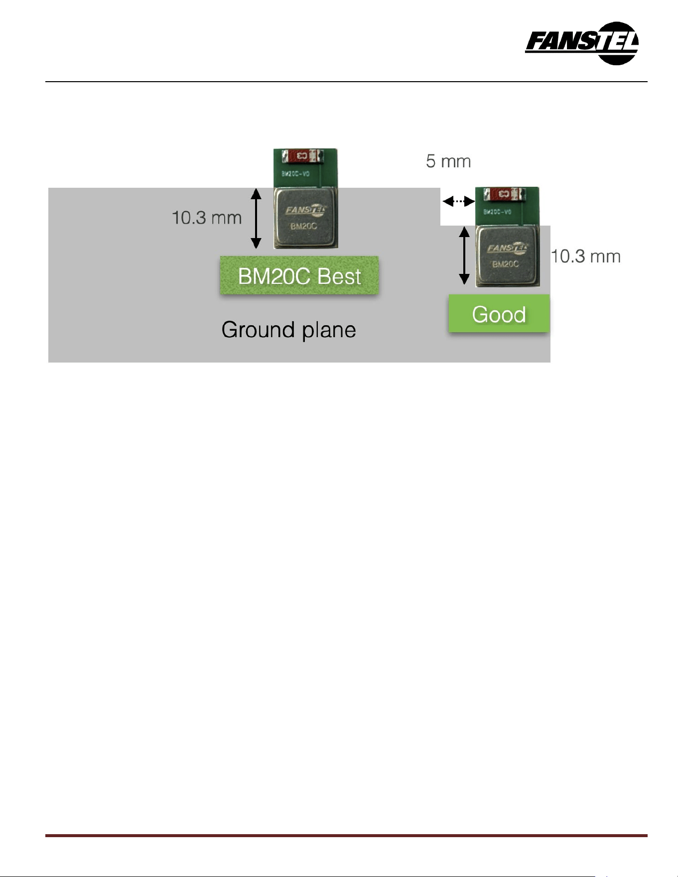
BM20C or BM20M with an integrated antenna is referred as BM20C in this section. It shall follow these mounting
guidelines. There is no mounting restriction for BM20E with an u.FL connector.
The length of the RFI shield is 10.3 mm. The RFI shield area is the main body of module. The rest of the module is called
antenna area.
• The main body area can be on a host board ground plane. The antenna area must be extended outside of the host
board or in an area without ground or signal trace.
• The length of BM20C antenna area is 5.5 mm.
• The length of BM20M antenna area is 3.7mm.
• We don’t recommend mounting BM20C module in the middle of a host PCB.
For the best Bluetooth range performance, keep all external metal at least 30mm from the antenna area.
Suggestion for Battery Power Application
Standby current consumption is important for battery-powered product. Both 32 MHz and 32 KHz crystals are
embedded. Inductors required for DCDC converter are inside BM20C module. You can enable DCDC to lower
power consumption.
Bluetooth 6.0, 802.15.4 Module BM20C Draft Ver 0.81 June 2026
19
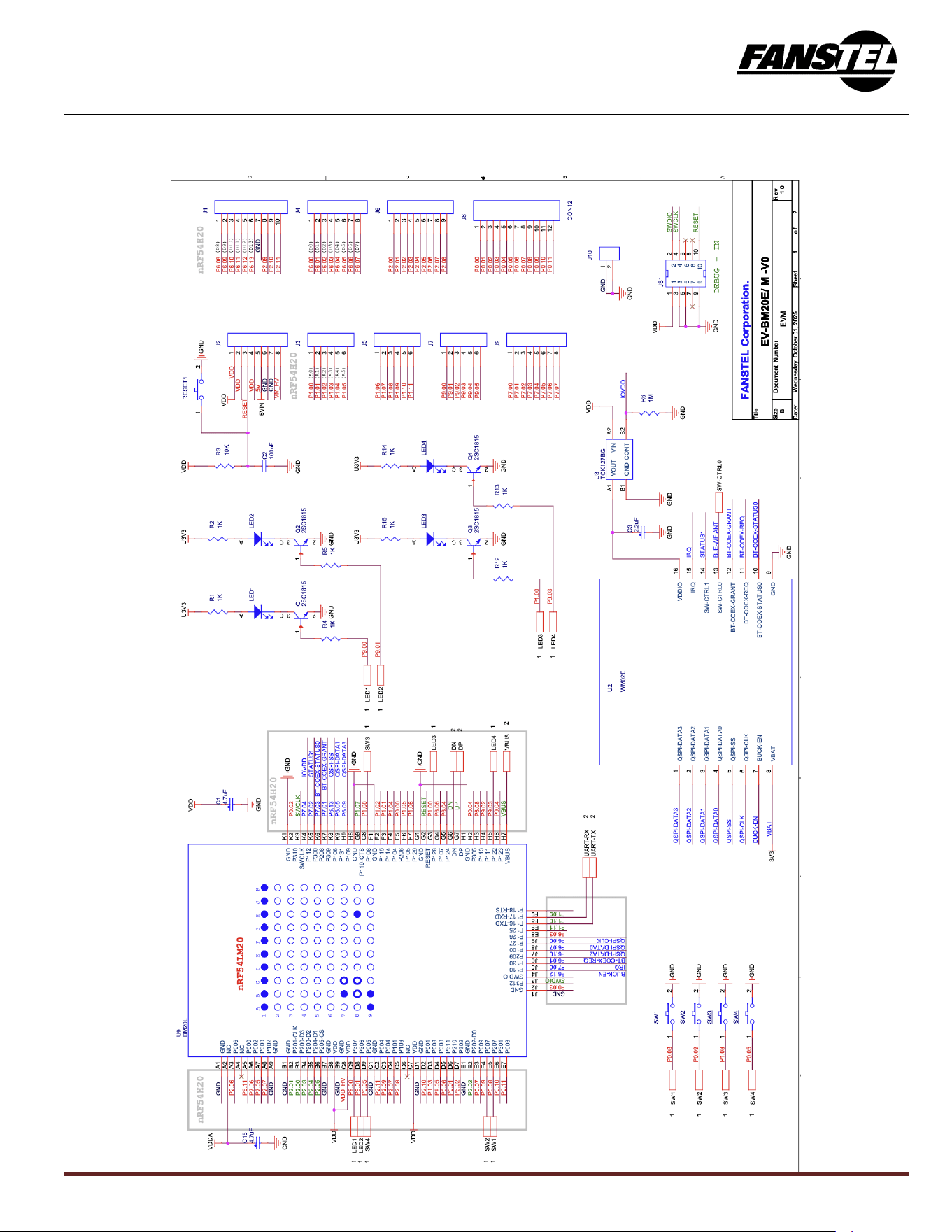
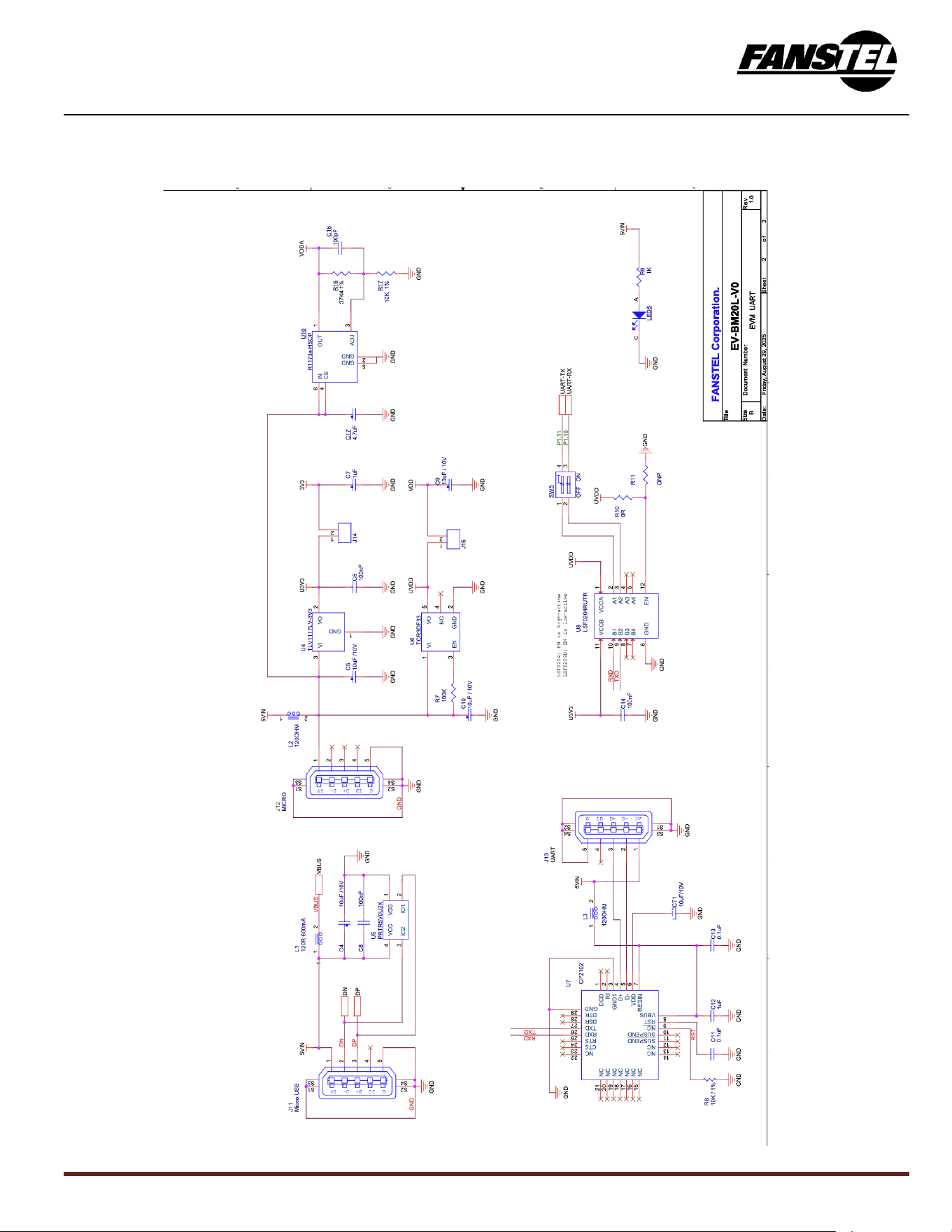
EV-BM20BC Evaluation Board Schematics
Bluetooth 6.0, 802.15.4 Module BM20C Draft Ver 0.81 June 2026
20
Page 2 of EV-BM20C

Bluetooth 6.0, 802.15.4 Module BM20C Draft Ver 0.81 June 2026
21
Evaluation Board
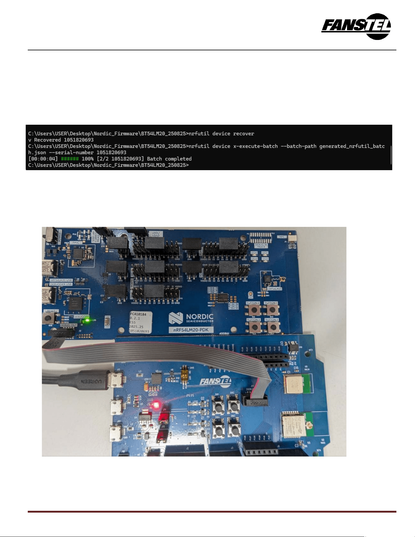
EV-BM20BC consists of the following:
• An evaluation board with BM20BC module and WM02C, an nRF7002 WiFi 6 module.
• A 10-pins flat cable for connection to nRF54LM20 DK.
• An USB cable.
• An nRF54LM20B module is used in all evaluation board. Don’t use the Axon NPU if you use an
nRF54LM20A module.
Bluetooth 6.0, 802.15.4 Module BM20C Draft Ver 0.81 June 2026
22
3. Firmware Development
An evaluation board can be used to evaluate performance of module and to develop and test your firmware
before an application-specific host board is developed.
Loading Firmware into Evaluation Board Through a Nordic DK
A Nordic nRF54LM20A PDK or DK is required to load firmware into EV-BM20C.
Procedures to connect a Nordic DK to a Fanstel nRF54 module evaluation board.
• Connect Nordic nRF54LM20A DK debug out to Fanstel evaluation board debug in using the 10-pin flat cable as shown
below.
• Connect Nordic nRF54LM20A DK to PC.
• Connect a DC power source to micro or mini USB port of evaluation board.
Bluetooth 6.0, 802.15.4 Module BM20C Draft Ver 0.81 June 2026
23
Procedures to Load Firmware
Open a command line tool and execute the programming commands:
nrfutil device recover
nrfutil device x-execute-batch --batch-path generated_nrfutil_batch.json --serial-number 1051820693
Note: The JSON file is generated in the build folder, and the serial number should match the DK’s serial number. You can
use the command nrfutil device list to check available serial numbers.
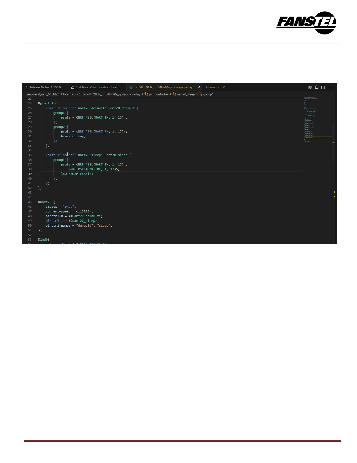
Setting Up Firmware Development Environment
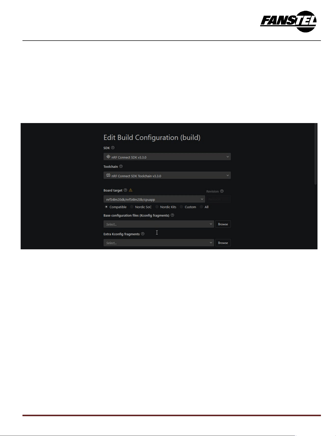
Please use nRF Connect SDK version 3.3.0 or newer for development. Older versions do not support the BM20C.
Bluetooth 6.0, 802.15.4 Module BM20C Draft Ver 0.81 June 2026
24
Select the board: nrf54lm20dk/nrf54l20a/cupapp (nRF54LM20 silicon).
Create an overlay file to configure hardware peripherals according to your specific setup. For example, you can create an
nrf54lm20dk/nrf54l20a.overlay file with the necessary configuration.
The example overlay for Wi-Fi.
Extra CMake arguments:-DSHIELD=nrf7002eb2
overlay:
&pinctrl {
spi22_default: spi22_default {
group1 {
psels = <NRF_PSEL(SPIM_MOSI, 1, 6)>,
<NRF_PSEL(SPIM_MISO, 1, 7)>,
<NRF_PSEL(SPIM_SCK, 1, 11)>;
};
};
spi22_sleep: spi22_sleep {
group1 {
psels = <NRF_PSEL(SPIM_MOSI, 1, 6)>,
<NRF_PSEL(SPIM_MISO, 1, 7)>,
<NRF_PSEL(SPIM_SCK, 1, 11)>;
low-power-enable;
};
};
};
&spi22 {
status = "okay";
pinctrl-0 = <&spi22_default>;
pinctrl-1 = <&spi22_sleep>;
pinctrl-names = "default", "sleep";
Bluetooth 6.0, 802.15.4 Module BM20C Draft Ver 0.81 June 2026
25
cs-gpios = <&gpio1 10 GPIO_ACTIVE_LOW>;
nrf70: nrf7002-spi@0 {
compatible = "nordic,nrf7002-spi";
reg = <0>;
spi-max-frequency = <8000000>;
status = "okay";
/* Manually specify required GPIOs to satisfy compiler requirements */
host-irq-gpios = <&gpio1 14 GPIO_ACTIVE_HIGH>;
bucken-gpios = <&gpio1 4 GPIO_ACTIVE_HIGH>;
iovdd-ctrl-gpios = <&gpio1 5 GPIO_ACTIVE_HIGH>;
/* Custom power configurations */
wifi-max-tx-pwr-2g-dsss = <0x15>;
wifi-max-tx-pwr-2g-mcs0 = <0x10>;
wifi-max-tx-pwr-2g-mcs7 = <0x10>;
};
};
&wlan0 {
status = "okay";
};
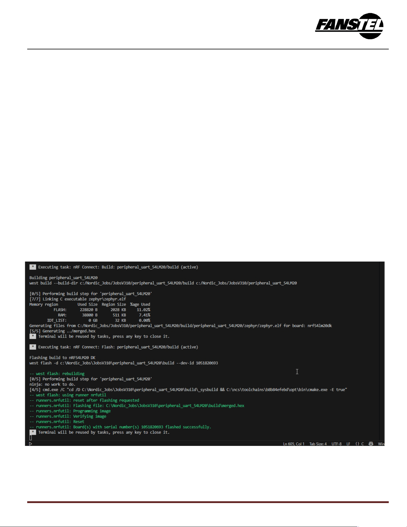
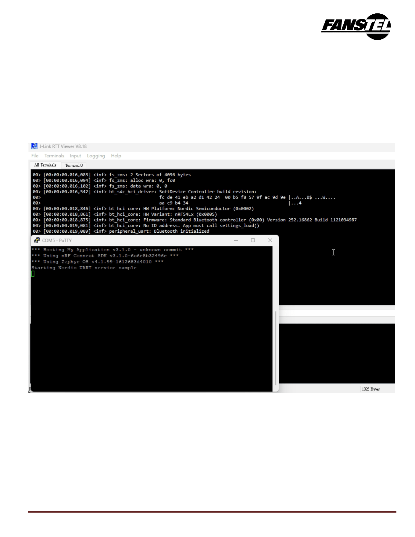
After completing the setup, build and flash the code, then verify that it is running correctly.
Bluetooth 6.0, 802.15.4 Module BM20C Draft Ver 0.81 June 2026
26
Preloaded Firmware
Production test codes are not erased when modules are shipped from factory. Before using the modules, please use the
following command to erase the preprogrammed codes.
nrfutil device recover
Bluetooth 6.0, 802.15.4 Module BM20C Draft Ver 0.81 June 2026
27
4. Miscellaneous
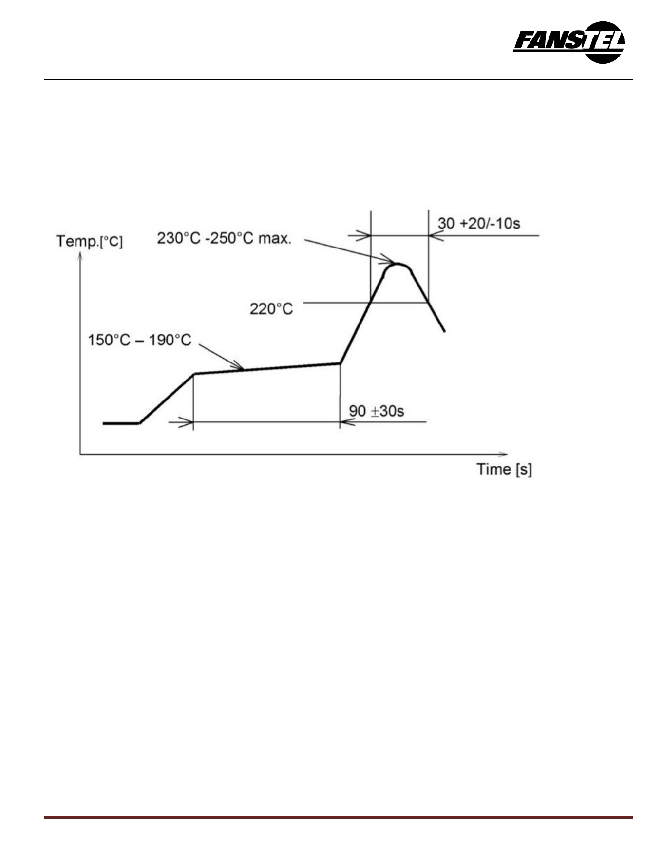
Soldering Temperature-Time Profile for Re-Flow Soldering
Maximum number of cycles for re-flow is 2. No opposite side re-flow is allowed due to module weight.
Cautions, Design Notes, and Installation Notes
Failure to follow the guidelines set forth in this document may result in degrading of the product’s
functions and damage to the product.
Design Notes
(1) Follow the conditions written in this specification, especially the control signals of this module.
(2) The supply voltage has to be free of AC ripple voltage (for example from a battery or a low noise
regulator output). For noisy supply voltages, provide a decoupling circuit (for example a ferrite in
series connection and a bypass capacitor to ground of at least 47uF directly at the module).
(3) This product should not be mechanically stressed when installed.
(4) Keep this product away from heat. Heat is the major cause of decreasing the life of these
products.
(5) Avoid assembly and use of the target equipment in conditions where the products' temperature
may exceed the maximum tolerance.
(6) The supply voltage should not be exceedingly high or reversed. It should not carry noise and/or
spikes.
(7) this product away from other high frequency circuits.

Bluetooth 6.0, 802.15.4 Module BM20C Draft Ver 0.81 June 2026
28
Notes on Antenna and PCB Layout
(1) Don’t use a module with internal antenna inside a metal case.
(2) For PCB layout:
• Avoid running any signal line below module whenever possible,
• No ground plane below antenna,
• If possible, cut-off the portion of main board PCB below antenna.
Installation Notes
(1) Reflow soldering is possible twice based on the time-temperature profile in this data sheets. Set up
the temperature at the soldering portion of this product according to this reflow profile.
(2) Carefully position the products so that their heat will not burn into printed circuit boards or affect
the other components that are susceptible to heat.
(3) Carefully locate these products so that their temperatures will not increase due to the effects of
heat generated by neighboring components.
(4) If a vinyl-covered wire comes into contact with the products, then the cover will melt and generate
toxic gas, damaging the insulation. Never allow contact between the cover and these products to
occur.
(5) This product should not be mechanically stressed or vibrated when reflowed.
(6) If you want to repair your board by hand soldering, please keep the conditions of this chapter.
(7) Do not wash this product.
(8) Refer to the recommended pattern when designing a board.
(9) Pressing on parts of the metal cover or fastening objects to the metal will cause damage to the
unit.
(10) For more details on LGA (Land Grid Array) soldering processes refer to the application note.
Usage Condition Notes
(1)Take measures to protect the unit against static electricity. If pulses or other transient loads (a
large load applied in a short time) are applied to the products, check and evaluate their operation
before assembly on the final products.
(2)Do not use dropped products.
(3)Do not touch, damage or soil the pins.
(4) Follow the recommended condition ratings about the power supply applied to this product.
(5)Electrode peeling strength: Do not add pressure of more than 4.9N when soldered on PCB
(6) Pressing on parts of the metal cover or fastening objects to the metal cover will cause damage.
(7) These products are intended for general purpose and standard use in general electronic
equipment, such as home appliances, office equipment, information and communication
equipment.
Storage Notes
(1)The module should not be stressed mechanically during storage.

Bluetooth 6.0, 802.15.4 Module BM20C Draft Ver 0.81 June 2026
29
(2)Do not store these products in the following conditions or the performance characteristics of the
product, such as RF performance will be adversely affected:
• Storage in salty air or in an environment with a high concentration of corrosive gas.
• Storage in direct sunlight
• Storage in an environment where the temperature may be outside the range specified.
• Storage of the products for more than one year after the date of delivery storage period.
(3) Keep this product away from water, poisonous gas and corrosive gas.
(4) This product should not be stressed or shocked when transported.
(5) Follow the specification when stacking packed crates (max. 10).
Safety Conditions
These specifications are intended to preserve the quality assurance of products and individual
components.
Before use, check and evaluate the operation when mounted on your products. Abide by
these specifications, without deviation when using the products. These products may short-circuit. If
electrical shocks, smoke, fire, and/or accidents involving human life are anticipated when a short
circuit occurs, then provide the following failsafe functions, as a minimum.
(1)Ensure the safety of the whole system by installing a protection circuit and a protection device.
(2)Ensure the safety of the whole system by installing a redundant circuit or another system to
prevent a dual fault causing an unsafe status.
Other Cautions
(1)This specification sheet is copyrighted. Reproduction of this data sheets is permissible only if
reproduction is without alteration and is accompanied by all associated warranties, conditions,
limitations, and notices.
(2)Do not use the products for other purposes than those listed.
(3)Be sure to provide an appropriate failsafe function on your product to prevent an additional damage
that may be caused by the abnormal function or the failure of the product.
(4)This product has been manufactured without any ozone chemical controlled under the Montreal
Protocol.
(5)These products are not intended for other uses, other than under the special conditions shown
below. Before using these products under such special conditions, check their performance and
reliability under the said special conditions carefully to determine whether or not they can be used
in such a manner.
• In liquid, such as water, salt water, oil, alkali, or organic solvent, or in places where liquid may
splash.
• In direct sunlight, outdoors, or in a dusty environment
• In an environment where condensation occurs.
• In an environment with a high concentration of harmful gas.

Bluetooth 6.0, 802.15.4 Module BM20C Draft Ver 0.81 June 2026
30
(6) If an abnormal voltage is applied due to a problem occurring in other components or circuits,
replace these products with new products because they may not be able to provide normal
performance even if their electronic characteristics and appearances appear satisfactory.
(7) When you have any question or uncertainty, contact Fanstel.
Packaging
Production modules are delivered in reel, 1000 modules in each reel.
FCC LABEL
The Original Equipment Manufacturer (OEM) must ensure that the OEM modular transmitter must be labeled
with its own FCC ID number. This includes a clearly visible label on the outside of the final product enclosure
that displays the contents shown below. If the FCC ID is not visible when the equipment is installed inside
another device, then the outside of the device into which the equipment is installed must also display a label
referring to the enclosed equipment
The end product with this module may subject to perform FCC part 15 unintentional emission test requirement
and be properly authorized.
This device is intended for OEM integrator only.

Bluetooth 6.0, 802.15.4 Module BM20C Draft Ver 0.81 June 2026
31
5. Revision History
• Dec. 2025, Ver. 0.51: The initial draft specs release.
• March 2026, Ver 0.80: Draft revision.
• May 2026, Ver 0.81: Add upgrading information to BM20NE and BM20XE Series.

Bluetooth 6.0, 802.15.4 Module BM20C Draft Ver 0.81 June 2026
32
6.Contact Us
Fanstel Corp.
7466 E. Monte Cristo Ave. Scottsdale AZ 85260
Tel. 1 480-948-4928
Fax. 1-480-948-5459
Email: info@fanstel.com
Website: www.fanstel.com
Taiwan:
Fanstel Corp.
10F-10, 79 Xintai Wu Road
Xizhu, New Taipei City, Taiwan 22101
泛世公司
臺灣省新北市汐止區新臺五路 79 號 10 樓之 10, 22101
Tel. 886-2-2698-9328
Fax. 886-2-2698-4813
Email: info@fanstel.com
Website: www.fanstel.com
China:
Fanstel Technologies Corp.
11 Jiale Street
Ping-Dih, Long-Gang, Shen Zhen, GD 518117
泛世康科技(深圳)有限公司
廣東省深圳市龍崗區坪地鎮佳樂街 11 號
Tel. 86-755-8409-0928
Fax. 86-755-8409-0973
QQ. 3076221086
Email: info@fanstel.com
Website: www.fanstel.com

Bluetooth 6.0, 802.15.4 Module BM20C Draft Ver 0.81 June 2026
33
Federal Communications Commission (FCC) Statement
15.21
You are cautioned that changes or modifications not expressly approved by the part responsible for compliance
could void the user’s authority to operate the equipment.
15.105(b)
This equipment has been tested and found to comply with the limits for a Class B digital device, pursuant to part 15 of the
FCC rules. These limits are designed to provide reasonable protection against harmful interference in a residential
installation. This equipment generates, uses and can radiate radio frequency energy and, if not installed and used in
accordance with the instructions, may cause harmful interference to radio communications.
However, there is no guarantee that interference will not occur in a particular installation. If this equipment does cause
harmful interference to radio or television reception, which can be determined by turning the equipment off and on, the
user is encouraged to try to correct the interference by one or more of the following measures:
-Reorient or relocate the receiving antenna.
-Increase the separation between the equipment and receiver.
-Connect the equipment into an outlet on a circuit different from that to which the receiver is connected.
-Consult the dealer or an experienced radio/TV technician for help.
This device complies with Part 15 of the FCC Rules. Operation is subject to the following two conditions:
1) this device may not cause harmful interference, and
2) this device must accept any interference received, including interference that may cause undesired operation
of the device.
FCC RF Radiation Exposure Statement
The antenna(s) used for this transmitter must be installed to provide a separation distance of at least 20 cm from all
persons and must not be co-located or operating in conjunction with any other transmitter, except in accordance with FCC
multi-transmitter product procedures.
This equipment should be installed.
Note: The end product shall has the words “Contains Transmitter Module FCC ID:
X8WBM20C

Bluetooth 6.0, 802.15.4 Module BM20C Draft Ver 0.81 June 2026
34
Canada, Industry Canada (IC)
This Class B digital apparatus complies with Canadian ICES-003
Cet appareil numérique de classe B est conforme à la norme NMB-003.
This device complies with Industry Canada licence-exempt RSS standard(s). Operation is subject
to the following two conditions: (1) this device may not cause interference, and (2) this device
must accept any interference, including interference that may cause undesired operation of the
Le present appareil est conforme aux CNR d'Industrie Canada applicables auxappareils radio exempts de
licence.L'exploitation est autorisée aux deux conditions suivantes:
(1) l'appareil ne doit pas produire de brouillage, et
(2) l'utilisateur de l'appareil doit accepter tout brouillage adioélectrique subi, même si le brouillage est susceptible d'en
compromettre le fonctionnement.
Conformité des appareils de radiocommunication aux limites
d'exposition humaine aux radiofréquences (CNR-102)
L'ordinateur utilise des antennes intégrales à faible gain qui n'émettent pas un
champ électromagnétique supérieur aux normes imposées par Santé Canada
pour la population. Consultez le Code de sécurité 6 sur le site Internet de Santé
Canada à l'adresse suivante : http://www.hc-sc.gc.ca/
L'énergie émise par les antennes reliées aux cartes sans fil respecte la limite
d'exposition aux radiofréquences telle que définie par Industrie Canada dans la
clause 4.1 du document CNR-102, version 4.
Caution: Exposure to Radio Frequency Radiation.
L'antenne ou les antennes utilisées pour cet émetteur doivent être installées de manière à assurer une distance de
séparation d'au moins 20 cm par rapport à toutes les personnes et ne doivent pas être situées à proximité ou
fonctionner en conjonction avec un autre émetteur, sauf conformément aux procédures de la FCC relatives aux
produits multi-émetteurs. Cet équipement doit être installé.
(Modular approval) End Product Labeling:
The final end product must be labeled in a visible area with the following: “Contains IC: 4100A-BM20C
Le produit final doit être étiqueté dans une zone visible avec ce qui suit “Contient IC : 4100A-BM20C

Bluetooth 6.0, 802.15.4 Module BM20C Draft Ver 0.81 June 2026
35
OEM statement
The Original Equipment Manufacturer (OEM) must ensure that the OEM modular transmitter must be labeled with its
own FCC ID number. This includes a clearly visible label on the outside of the final product enclosure that displays the
contents shown below. If
the FCC ID is not visible when the equipment is installed inside another device, then the outside of the device into which
the equipment is installed must also display a label referring to the enclosed equipment.
The end product with this module may subject to perform FCC part 15B unintentional emission test requirement and be
properly authorized while installation to host(s), and platform, and integrator are obligated to have its manual or
instruction with the related compliance warning to end users.
This device is intended for OEM integrator only
The end product with this module may be subject to re-evaluate RF exposure as per 47CFR §
2.1091, and §2.1093 if antenna or usage, including co-located usage of other transmitters, of the subsequent
installation are changed.
This radio transmitter has been approved by FCC/Innovation, Science and Economic Development Canada to operate with
the antenna types listed below, with the maximum permissible gain indicated. Antenna types not included in this list that
Have a gain greater than the maximum gain indicated for any type listed are strictly prohibited for use with this device.
F-PCB antennas: 4.31 dBi M-PCB antennas: -1.72 dBi
Cet émetteur radio a été approuvé par FCC/Innovation, Science et Développement économique Canada pour fonctionner
avec les types d'antennes répertoriés ci-dessous, avec le gain maximal autorisé indiqué. Les types d'antenne non inclus
dans cette liste qui ont un gain supérieur au gain maximum indiqué pour tout type répertorié sont strictement interdits pour
une utilisation avec cet appareil.
F-PCB antennas: 4.31 dBi M-PCB antennas: -1.72 dBi
NCC 警語:
低功率產品警語:「取得審驗證明之低功率射頻器材,非經核准,公司、商號或使用者
均不得擅自變更頻率、加大功率或變更原設計之特性及功能。低功率射頻器材之使用不
得影響飛航安全及干擾合法通信;經發現有干擾現象時,應立即停用,並改善至無干擾
時方得繼續使用。前述合法通信,指依電信管理法規定作業之無線電通信。低功率射頻
器材須忍受合法通信或工