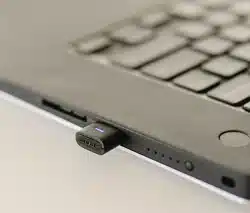


TPL3135 BLE Module Datasheet
1、Introduction
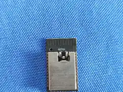
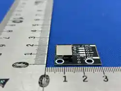
2、Module Parameters
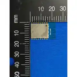
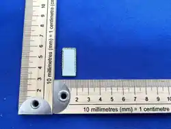
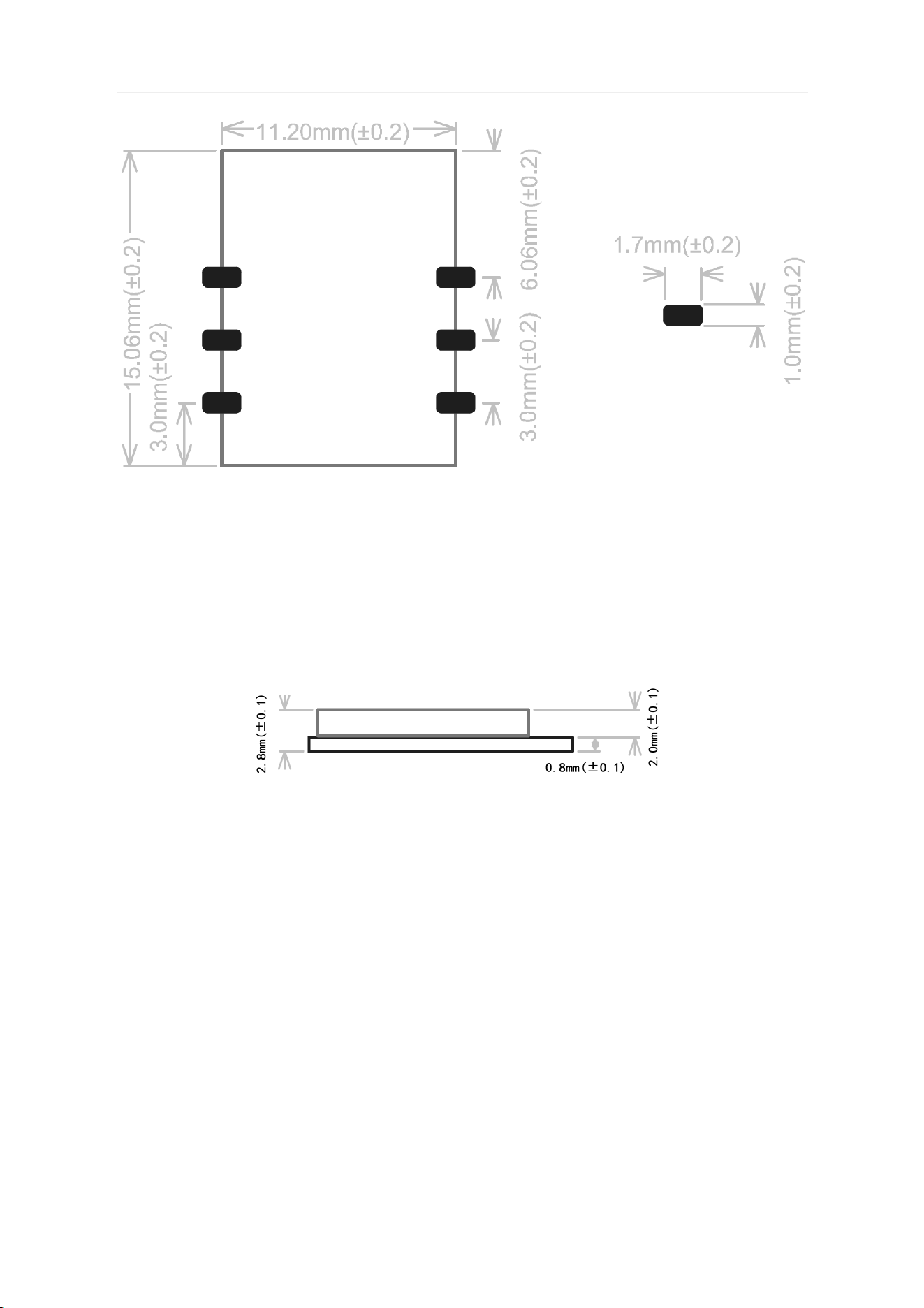
3、Module Size
4、Pin Definition
5、Reference Design
5.1、VBAT Power Supply Reference Design
5.2、VCC Power Supply Reference Design
6、Hardware Design Considerations
6.1、Module placement requirements on the bottom plate
6.2、Power supply requirements
6.3、UART Communication
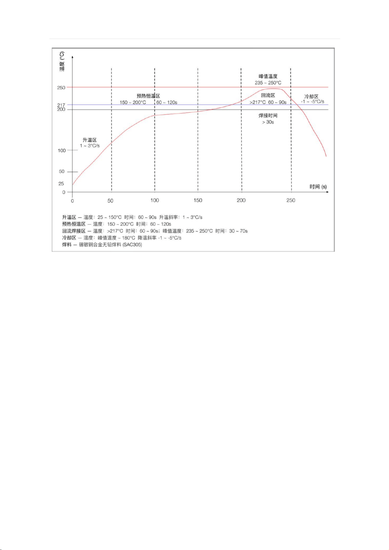
7、Reflow Profile
8、Revision History
Item Parameters
Module Name TPL3131
Package SMT(Stamp Hole)
Size 11.2x15.06(mm)
Voltage Range VBAT( 2.7V~5.5V)或 VCC ( 1.9V~3.5V)
Wireless Standard Bluetooth 5.4
Frequency Range 2402~2480MHz
Sensitivity -92dBm
Default Communication interface UART
FLASH Size 256KB
RAM Size 32KB
Operating current 3.5mA
Sleep current 3uA
Shutdown current 200nA
GPIO Number 2
Work Temperature -20℃~+85℃
Storage Temperature -60℃~+150℃
1、Introduction
TPL3131 is a BLE 5.4 low power Bluetooth module, which can be widely used in short
distance wireless Bluetooth communication. It has the characteristics of small size, low power
consumption, strong anti-interference ability and long transmission distance.
The other main features of the module are as follows:
compliant with Bluetooth 5 .4 standard, which can support various Profile configurations.
Support low power Bluetooth data transparent transmission
Support AT command control
Support online OTA upgrade module firmware
Ultra small package
2、Module Parameters
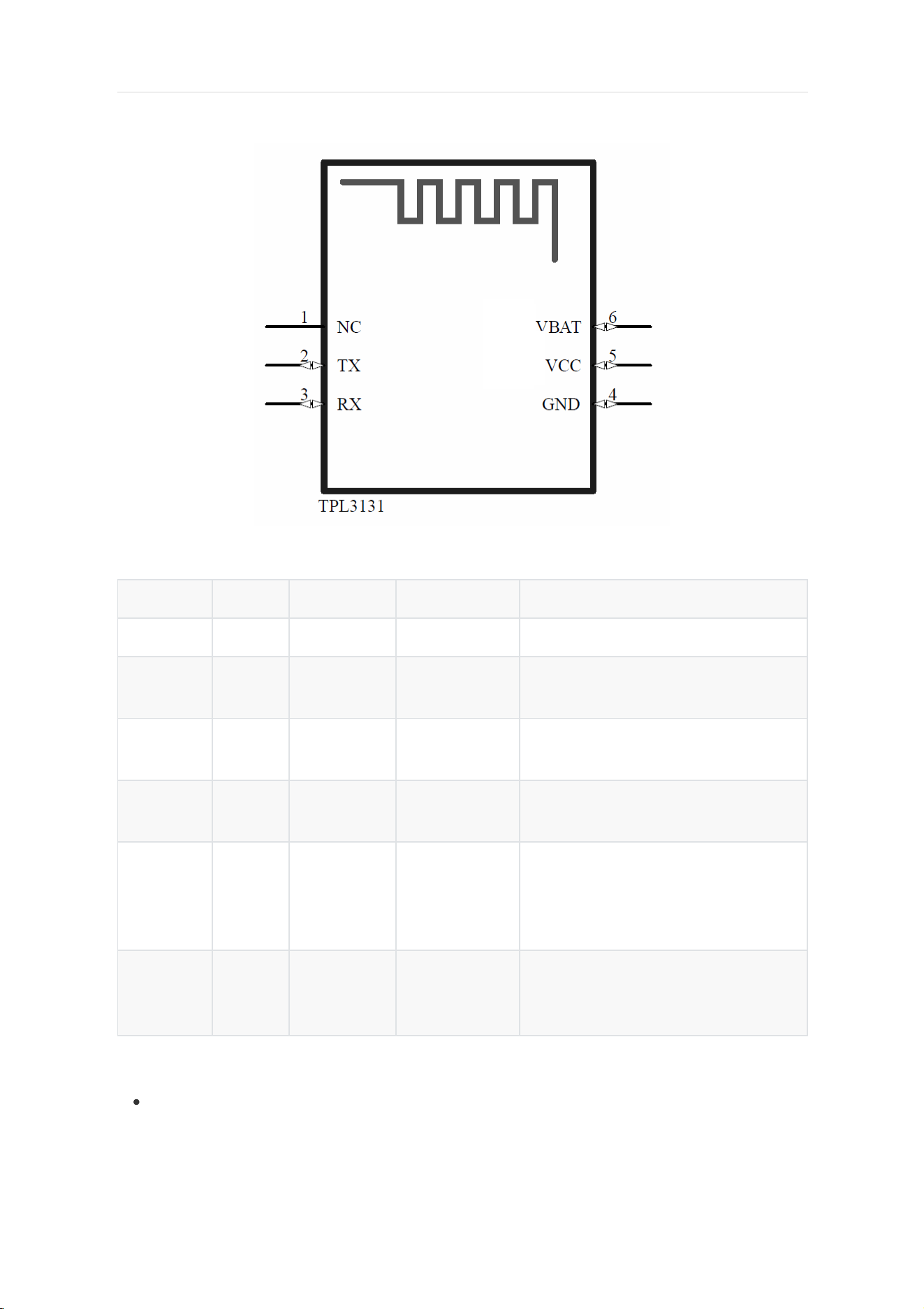
Number Name Pin Function Notes
1 NC NC NC Not connected
2 TX UART_TX
Serial port
transmission
3 RX UART_RX
Serial port
receiving
4 GND Ground
Power
'Ground'
5 VCC VCC
Power
supply(
1.9V~3.5V)
Two AA batteries/button cell
batteries are recommended. When
powered by VBAT, it outputs 3.3V
voltage externally.
6 VBAT VBAT
Power
supply (
2.7V~5.5V)
5V/3.3V power supply, 4.2V lithium
battery, three dry cells
recommended for use
4、Pin Definition
Explanation:
When powered by VBAT, the VCC pin outputs 3.3V externally and can only be used as a signal
source, with a maximum output current of 10mA.
5、Reference Design
The TPL3131 module can be powered through either the VBAT pin or the VCC pin. The VBAT
pin supports 2.7-5.5V, and it is recommended to use the VBAT pin for 5V and 3.3V systems. The
VCC pin supports 1.9V-3.5V, and it is recommended to use the VCC pin when powering with two
dry batteries or button batteries.
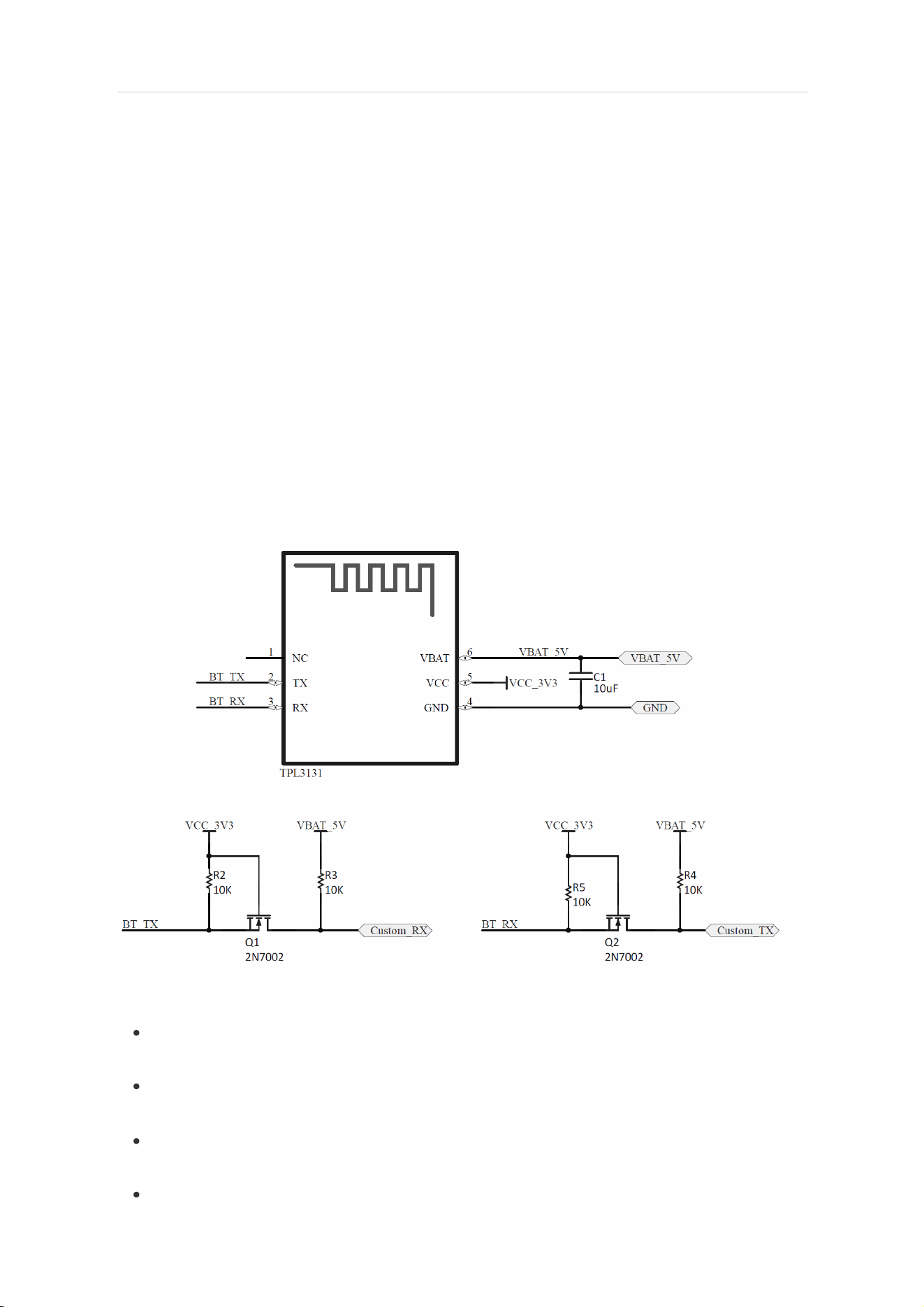
5.1、VBAT Power Supply Reference Design
For 5V or 3.3V system power supply, the VBAT power supply pin is used. When the VBAT
power supply is greater than 3.3V, the TPL3131 chip serial port level is 3.3V. When the VBAT
power supply is less than 3.3V, the TPL3131 chip serial port level equals the VBAT voltage.
When connected to an MCU with 3.3V level IO, UART can be connected in series with a 100Ω
resistor.
When connecting to an MCU with 5V level IO, it is recommended to use a level conversion
circuit. The schematic provides a 3.3V to 5V conversion circuit using MOSFETs. Among them, the
MCU serial ports Custom_Tx and Custom_Rx used for Bluetooth communication are at 5V level.
When the VBAT pin is powered, the internal LDO of the chip will be activated, and VCC
outputs a 3.3V voltage externally.
说明:
In the diagram, VCC_3V3 is the voltage output externally converted by the internal LDO of the
chip. The customer only needs to provide 5V voltage from VBAT.
The circuit with two 2N7002 MOSFETs is a serial port level conversion circuit designed, and it
can be replaced with other conversion circuits.
The TPL3131 serial port IO level is 3.3V. It is recommended to use a conversion circuit when
connecting to a 5V level.
If a modular power-off method is used to control shutdown power consumption, it is
recommended to disconnect the GND circuit to prevent leakage current due to voltage
differences at the IO interfaces.
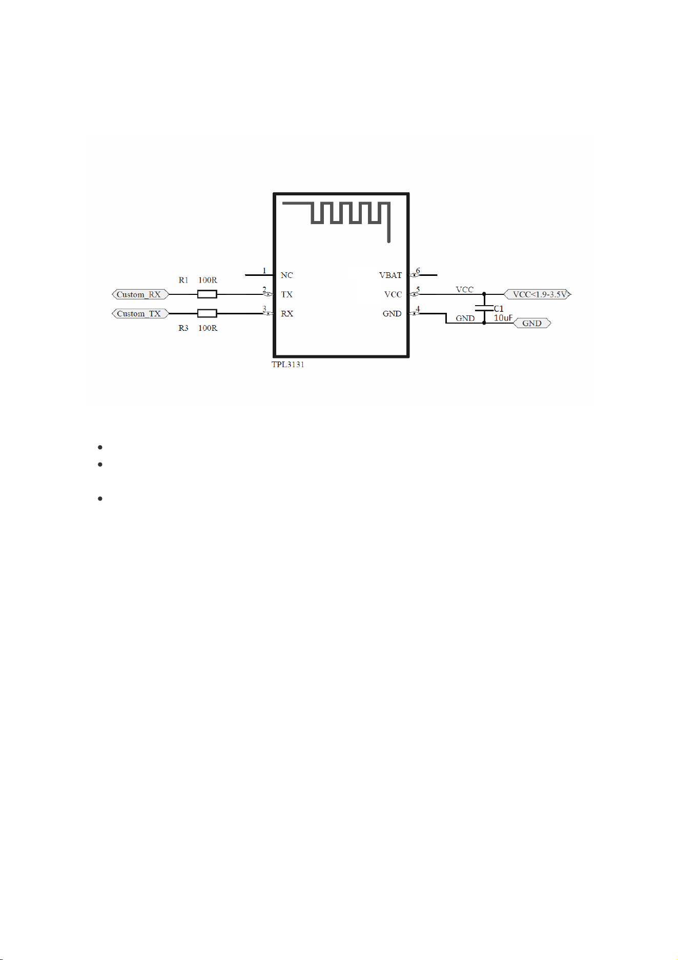
5.2、VCC Power Supply Reference Design
Two dry batteries or button batteries are recommended to power via the VCC pin, and the MCU
serial ports Custom_Tx and Custom_Rx used for Bluetooth communication need to be equal to or
lower than the VCC voltage.
说明:
The VCC (1.9V~3.5V) pin is powered, and the VBAT is left floating and not connected.
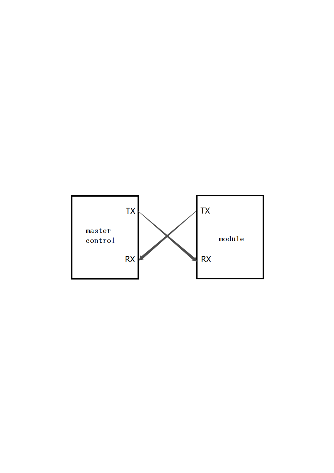
The TX and RX of the chip need to be cross-connected with the main control MCU, and the
series-connected resistors R1 and R3 in between can be added according to requirements.
If using a module power-off method to control shutdown power consumption, it is
recommended to disconnect the GND circuit to prevent leakage current caused by voltage
differences at the IO interface.
6、Hardware Design Considerations
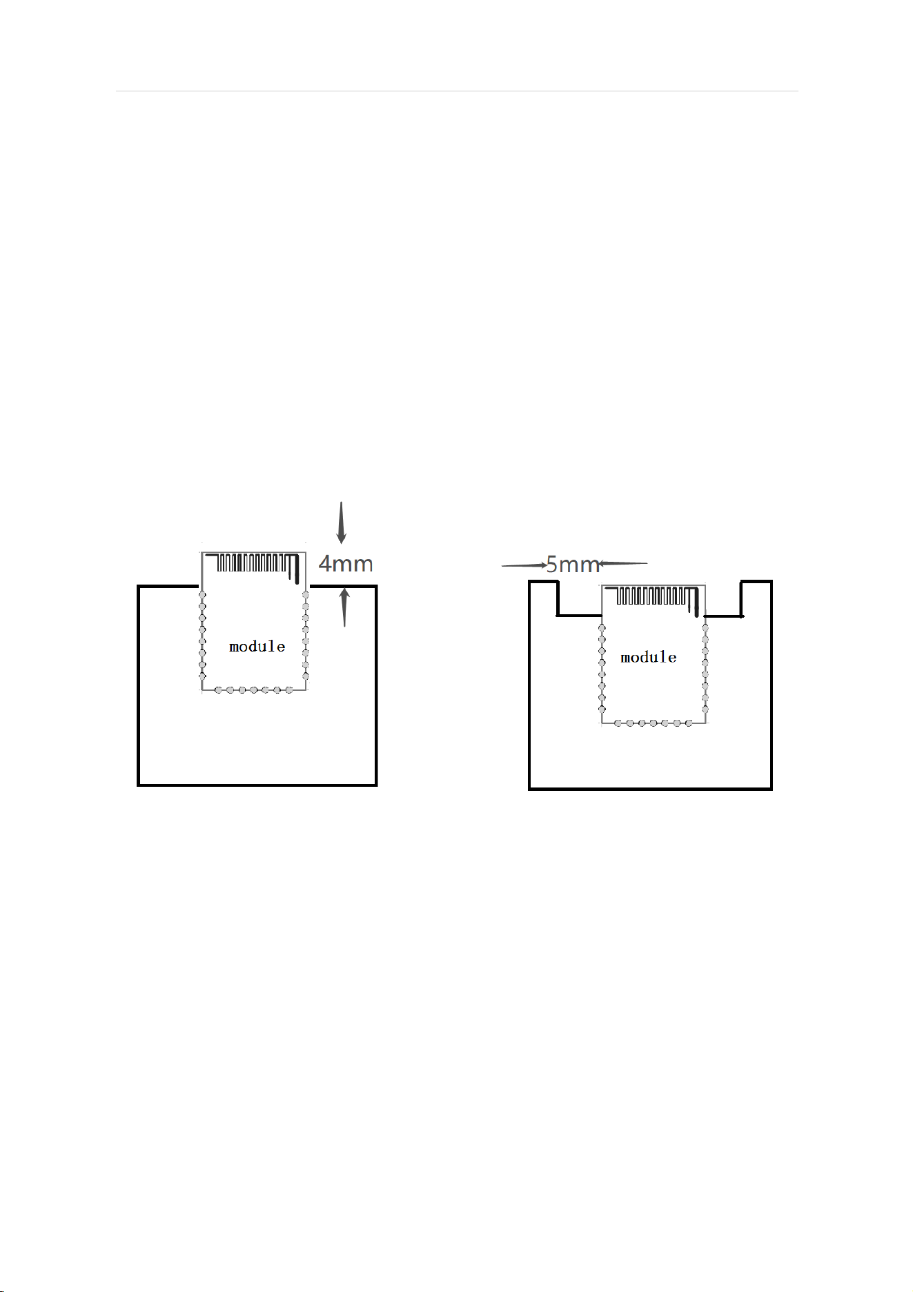
6.1、Module placement requirements on the bottom plate
(1) In order to meet the performance of the antenna on board, it is forbidden to place metal
parts around the antenna, away from high frequency devices.Avoid using metal in the product
housing and keep metal screw inside away from the RF part of the module.
(2) Pay attention to the layout of the module on the soleplate, and minimize the impact of the
soleplate on the performance of the module PCB antenna.
The following are suggested:
Option 1: Place the module at the edge of the motherboard and the antenna area extends
beyond the edge of the motherboard.
Option 2: Place the module at the edge of the motherboard, which empties an area at the
antenna position.
Option 3: If the above scheme is limited and cannot be implemented, make sure that the area
of the module PCB antenna and the area of 5 mm extension need to be cleared (copper, wiring
and placement of components are strictly prohibited).
6.2、Power supply requirements
(1) It is recommended to use DC regulator power supply to supply power to the module. The
power ripple factor is as small as possible and the module needs to be grounded reliably. Please
note that the correct connection between the positive and negative poles of the power supply,
such as reverse connection may cause permanent damage to the module.
(2) Check the power supply to ensure that between the recommended supply voltage, if the
maximum value is exceeded, the module will be permanently damaged; check the power supply
stability, the voltage should not fluctuate significantly and frequently;
(3) Recommend 3.3V voltage for VBAT, LDO power supply is recommended; if using DC-DC,
ripple control is recommended within 30mV.The DC-DC power supply circuit suggests reserving
the position of the dynamic response capacitance to optimize the output ripple when the load
varies greatly.
6.3、UART Communication
UART communication between module and master MCU through serial port supports full
duplex transmission and reception of TX and RX.

Data Description Revision
2025-9-27 Initial Release V1.0
2026-1-22 Increase current parameter V1.1
2026-1-29 Modification of Reference Circuit Description V1.2
2026-3-3 Errata V1.3
8、Revision History
FCC Statement
FCC standards: FCC CFR Title 47 Part 15 Subpart C Section 15.247 ,
This device complies with part 15 of the FCC Rules. Operation is subject to the following two
conditions: (1) Thisdevice may not cause harmful interference, and (2) this devicemust accept any
interference received, including interference that may cause undesired operation.Any Changes or
modifications not expressly approved by the party responsible for compliance could void
theuser's authority to operate the equipment.
Note: This equipment has been tested and found to comply with the limits for a Class B digital
device, pursuant topart 15 of the FCC Rules. These limits are designed to provide
reasonableprotection against harmful interference in a residential installation. This equipment
generates, uses and canradiate radio frequency energy and, if not installed and used
inaccordance with the
instructions, may cause harmful interference to radio communications. However, there is no
guarantee thalinterference will not occur in a particular installation. If this equipment
does causeharmful interference to radio or television reception, which can be determined by
turning the equipment off and on,the user is encouraged to try to correct the interference by one
or more of the
following measures:
-Reorient or relocate the receiving antenna.
Increase the separation between the equipment and receiver.Connect the equipment into an
outlet on a circuit diferent from that to which the receiver is connectedConsult the dealer or an
experienced radio/TV technician for help.FCC Radiation Exposure Statement
This modular complies wih FCC RF radiation exposure limits set forth for an uncontrolled
environment. Thistransmitter must not be co-located or operating in conjunction withany other
antenna or
transmitter.
If the FCC identification number is not visible when the module is installed inside another device,
then the outsideof the device into which the module is installed must also displaya labelreferring
to the enclosed module. This exterior label can use wording such as the following: "Contains
Transmitter ModuleFCCID:2BG7T-TPL3131
When the module is installed inside another device, the user manual of the host must contain
below warningstatements;
1. This device complies with Part 15 of the FCC Rules. Operation is subject to the following two
conditions:(1) This device may not cause harmful interference;(2) This device must accept
any interference received, including interference that may cause undesired operation.Note:
This equipment has been tested and found to comply with the limits for a Class B digital

device, pursuant topart 15 of the FCC Rules. These limits are designed to provide
reasonableprotection against harmful interference in a residential installation. This
equipment generates, uses and canradiate radio frequency energy and, if not installed and
used inaccordance with the
instructions, may cause harmful interference to radio communications.However, there is no
guarantee that interference will not occur in a particular installation. If this equipment
doescause harmful interference to radio or television reception, whichcan be determined
antenna.
-Increase the separation between the equipment and receiver.-Connect the equipment into
an outlet on a circuit different from that to which the receiver is connected.-Consult the
dealer or an experienced radio/TV technician for help.2. Changes or modifications not
expressly approved by the party responsible for compliance could void the user's
authority to operate the equipment.The devices must be installed and used in strict
accordance with the manufacturer's instructions as described inthe user documentation that
comes with the product.Any company of the host device which install the modular with
modular approval should perform the test ofradiated & conducted emission and spurious
emission, etc. accordingto FCCpart 15C:
15.247 and 15.209 & 15.207,15B Class B requirement, Only if the test