
www.agenewtech.com
AGENEWTECH
H1503BQ
Hardware Design Guide_V1.1

H1503BQ_Hardware Design Guide
WWW.AGENEWTECH.COM
1
Our aim is to provide customers with timely and comprehensive service. For any assistance,
please contact our company headquarters:
(Agenewtech Building) No.52, Huigu Pioneer Park C, Huishan Economic Development Zone,
Wuxi City, Jiangsu, China
Postal Code: 214174
PhoneNum: +86 0510 8235 0372 Mailbox: [email protected]
Introduction
AGENEW OFFERS THE DOCUMENT AS A SERVICE TO ITS CUSTOMERS. CUSTOMERS MUST
DESIGN THEIR PRODUCTS ACCORDING TO THE SPECIFICATIONS AND PARAMETERS
PROVIDED IN THE DOCUMENTS. AGENEW SHALL NOT BE LIABLE FOR ANY DAMAGE CAUSED
BY FAILURE TO COMPLY WITH RELEVANT OPERATION OR DESIGN SPECIFICATIONS.
AGENEW HAS THE RIGHT TO UPDATE THE DOCUMENT BEFORE IT IS ANNOUNCED.
Disclaimers
AGENEW MAKES EFFORT TO ENSURE THE INTEGRITY, ACCURACY, TIMELINESS OR UTILITY
OF THE FUNCTIONS UNDER DEVELOPMENT, BUT DOES NOT EXCLUDE THE POSSIBILITY OF
ERRORS OR OMISSIONS OF THE ABOVE FUNCTIONS. UNLESS OTHERWISE SPECIFIED
VALID AGREEMENTS, AGENEW MAKES NO IMPLIED OR EXPRESS GUARANTEE FOR THE USE
OF FUNCTIONS UNDER DEVELOPMENT. TO THE MAXIMUM EXTENT PERMITTED BY
APPLICABLE LAWS, AGENEW SHALL NOT BE LIABLE FOR ANY LOSS OR DAMAGE SUFFERED
DUE TO THE USE OF THE FUNCTIONS UNDER DEVELOPMENT, WHETHER SUCH LOSS OR
DAMAGE IS FORESEEABLE OR NOT.
Copyright
THE INFORMATION CONTAINED HERE IS PROPRIETARY TECHNICAL INFORMATION OF WUXI
SUNNING SMART DEVICES CO.,LTD. ANY COPIES AND REPRINTS THIS DOCUMENT WITHOUT
THE PERMISSION OF AGENEW WILL BEAR LEGAL RESPONSIBILITY.
Copyright © Wuxi Sunning Technology Co.,Ltd. 2021. All rights reserved.
Copyright © Wuxi Sunning T echnology Co.,Ltd. 2021. All rights reserved.

H1503BQ_Hardware Design Guide
WWW.AGENEWTECH.COM
2
About the Document
History
Version Date Author Description
- 2024-05-21 Daniel Wu Initial
1.0 2024-06-22 Daniel Wu Controlled version
1.1 2024-08-26 Daniel Wu Correct errors

H1503BQ_Hardware Design Guide
WWW.AGENEWTECH.COM
1
Content
Content ........................................................................................................................................................ 1
Table ............................................................................................................................................................. 1
Figure ........................................................................................................................................................... 1
1 Introduction ............................................................................................................................................. 4
1.1 Safety precautions ............................................................................................................................. 5
2 Product concept ..................................................................................................................................... 5
2.1 Summary .............................................................................................................................................. 6
2.2 Main Performance .............................................................................................................................. 7
2.3 Functional block diagram .............................................................................................................. 10
3 Application Interfaces ......................................................................................................................... 11
3.1 Overview ........................................................................................................................................... 11
3.2 Pin Assignment ................................................................................................................................ 12
3.3 Pin Description ................................................................................................................................. 13
3.4 Power Supply ................................................................................................................................... 23
3.5 Power On and Off ........................................................................................................................... 24
3.5.1 Power On ....................................................................................................................................... 24
3.5.2 Power Off ....................................................................................................................................... 25
3.6 VRTC Interface ................................................................................................................................ 25
3.7 Power Output ................................................................................................................................... 26

H1503BQ_Hardware Design Guide
WWW.AGENEWTECH.COM
2
3.8 Charging and battery management ............................................................................................ 27
3.9 USB Interface ................................................................................................................................... 29
3.10 UART Interface .............................................................................................................................. 31
3.11 SIM Interface .................................................................................................................................. 32
3.12 SD Card Interface ......................................................................................................................... 34
3.13 GPIO Interface ............................................................................................................................... 37
3.14 I2C Interface .................................................................................................................................. 38
3.15 SPI Interface .................................................................................................................................. 39
3.16 ADC Interface ................................................................................................................................ 40
3.17 Motor Drive Interface ................................................................................................................... 40
3.18 LCM Interface ................................................................................................................................ 41
3.19 Touchscreen Interface ................................................................................................................. 42
3.20 Camera Interface .......................................................................................................................... 43
3.20.1 Design Considerations ............................................................................................................. 49
3.20.2 Flashlight Interface .................................................................................................................... 50
3.21 Sensor Interface ............................................................................................................................ 50
3.22 Audio Interface............................................................................................................................... 51
3.22.1 Microphone Interface Reference Circuit ............................................................................... 52
3.22.2 Handset Interface Reference Circuit ..................................................................................... 54
3.22.3 Headphone Interface Reference Circuit ............................................................................... 54
3.22.4 Speaker Interface Reference Circuit ..................................................................................... 56
3.22.5 Audio Signal Design Considerations ..................................................................................... 56

H1503BQ_Hardware Design Guide
WWW.AGENEWTECH.COM
3
3.23 Forced Download Interface ........................................................................................................ 57
3.24 LEDs Indicator Interface .............................................................................................................. 58
4 Wi-Fi and BT ........................................................................................................................................ 59
4.1 Wi-Fi Overview................................................................................................................................. 59
4.1.1 Wi-Fi Performance Metrics ........................................................................................................ 59
4.2 BT Overview ..................................................................................................................................... 61
4.2.1 BT Performance Metrics ............................................................................................................. 62
5 GNSS .................................................................................................................................................... 63
5.1 GNSS Performance Metrics ......................................................................................................... 63
5.2 GNSS RF Design Guidance ......................................................................................................... 63
6 Antenna Interface ................................................................................................................................ 65
6.1 Main/Diversity Interface ................................................................................................................. 65
6.1.1 RF reference circuits ................................................................................................................... 66
6.1.2 RF Signal Cable Layout Reference Guide ............................................................................. 67
6.2 Wi-Fi/BT/GNSS Antenna Interface .............................................................................................. 69
6.3 GNSS Antenna Interface ............................................................................................................... 70
6.3.1 Passive Antenna Reference Design ........................................................................................ 71
6.3.2 Active antenna reference design .............................................................................................. 71
6.4 Antenna Installation ........................................................................................................................ 72
6.4.1 Antenna Installation Requirements .......................................................................................... 72
6.4.2 The Recommended RF Connector For Antenna Mounting ................................................ 73
7 Electrical, Reliability & RF Performance ....................................................................................... 75

H1503BQ_Hardware Design Guide
WWW.AGENEWTECH.COM
4
7.1 Limit Parameters ............................................................................................................................. 75
7.2 Power rating ..................................................................................................................................... 75
7.3 Operating and storage temperature ............................................................................................ 75
7.4 Operating current ............................................................................................................................ 76
7.5 RF Transmit Power ......................................................................................................................... 78
7.6 RF Receive Sensitivity ................................................................................................................... 79
7.7 ESD Protection ................................................................................................................................ 80
8 Mechanical Dimensions .................................................................................................................... 81
8.1 Module Mechanical Dimensions .................................................................................................. 81
8.2 Top and Bottom View of The Module .......................................................................................... 82
9 Storage, Production and Packaging ............................................................................................... 84
9.1 Storage .............................................................................................................................................. 84
9.2 Production Welding ......................................................................................................................... 84
9.3 Packaging ......................................................................................................................................... 86
10 Appendix A ......................................................................................................................................... 87

H1503BQ_Hardware Design Guide
WWW.AGENEWTECH.COM
1
Table
Table 1 H1503BQ Supported Frequency Bands ··········································································· 6
Table 2 Main performance parameters ··························································································· 7
Table 3 I/O Parameter Definition ···································································································· 13
Table 4 Pin Description ······················································································································ 13
Table 5 Power Supply Description ································································································· 26
Table 6 Charging Interface Pin Definition ··················································································· 28
Table 7 USB Interface Pin Definition ····························································································· 30
Table 8 The Length Of The USB Trace Inside The Module ···················································· 31
Table 9 UART interface pin definition ··························································································· 32
Table 10 SIM Interface Pin Definition ··························································································· 33
Table 11 SD Card Interface Pin Definition ··················································································· 35
Table 12 The Length Of The SDIO Trace Inside The Module ················································ 36
Table 13 List of GPIO Interfaces ······································································································ 37
Table 14 I2C Interface Pin Definition ····························································································· 38
Table 15 SPI Interface Pin Definition ····························································································· 39
Table 16 ADC Interface Pin Definition ·························································································· 40
Table 17 Motor Drive Interface Pin Definition ··········································································· 40
Table 18 LCM Interface Pin Definition ·························································································· 41
Table 19 Touchscreen Interface Pin Definition ·········································································· 42
Table 20 Camera Interface Pin Definition ···················································································· 44

H1503BQ_Hardware Design Guide
WWW.AGENEWTECH.COM
2
Table 21 The Length of The MIPI Trace Inside The Module ·················································· 49
Table 22 Flashlight Interface Pin Definition ················································································ 50
Table 23 Sensor Interface Pin Definition ····················································································· 50
Table 24 Audio interface pin definition ························································································ 51
Table 25 Forced Download Pin Definitions ················································································· 57
Table 26 LEDs Indicator Interface Pin Definitions ····································································· 58
Table 27 Wi-Fi Transmit Performance ··························································································· 59
Table 28 WiFi Reception Performance ·························································································· 60
Table 29 BT Rate And Version Information ················································································· 62
Table 30 BT Transmit and Receive Performance Metrics ························································ 62
Table 31 GNSS Performance ············································································································ 63
Table 32 Main/Diversity Antenna Interface Pin Definition ···················································· 65
Table 33 H1503BQ Supported Frequency Bands ······································································ 65
Table 34 Wi-Fi/BT/GNSS Antenna Interface Pin Definition ··················································· 69
Table 35 Wi-Fi/BT Operating Frequency Bands ········································································ 69
Table 36 GNSS Antenna Interface Pin Definition ······································································ 70
Table 37 GNSS Operating Frequency Bands ·············································································· 70
Table 38 Antenna Requirements ····································································································· 72
Table 39 Limit Parameters ················································································································· 75
Table 40 Module Power Rating ······································································································· 75
Table 41 Operating and Storage Temperature ·········································································· 75
Table 42 H1503BQ Operating Current ························································································· 76

H1503BQ_Hardware Design Guide
WWW.AGENEWTECH.COM
3
Table 43 H1503BQ Module RF Transmit Power ········································································· 78
Table 44 H1503BQ RF Receive Sensitivity ··················································································· 79
Table 45 ESD Performance Parameters (Temperature: 25°C, Humidity: 45%) ················ 80
Table 46 Recommended Furnace Temperature Test Control Requirements ··················· 85
Table 47 Abbreviations for Terms ··································································································· 87

H1503BQ_Hardware Design Guide
WWW.AGENEWTECH.COM
1
Figure
Figure 1 Functional Block Diagram ······························································································· 10
Figure 2 H1503BQ Pinout Diagram (Top View) ········································································· 12
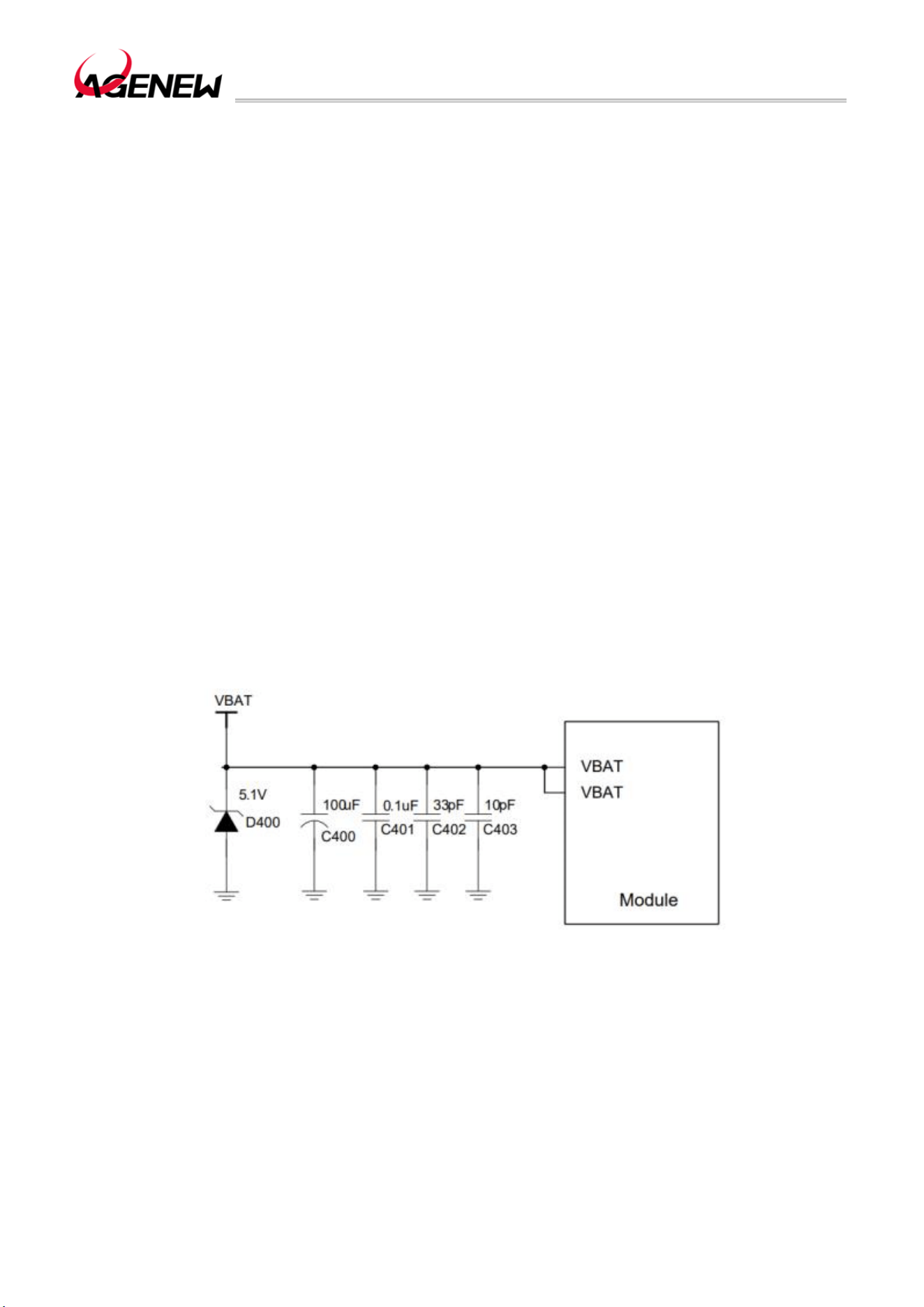
Figure 3 VBAT Input Reference Circuit ························································································· 23
Figure 4 The Open-Set Drive Refers To The Boot Circuit ······················································· 24
Figure 5 Boot Sequence Diagram ·································································································· 24
Figure 6 Sequence Diagram of Forced Shutdown ··································································· 25
Figure 7 A Rechargeable Coin Cell Battery Powers The RTC ················································ 25
Figure 8 Schematic Diagram Of Battery Charging Connection ··········································· 29
Figure 9 Mirco-USB Interface Reference Design ······································································ 30
Figure 10 USB Type-C Reference Design ····················································································· 31
11 Level Translation Reference Circuit (UART1) ········································································ 32
12 8-pin SIM Reference Circuit ······································································································· 34
Figure 13 Refer To The Circuit Diagram For The SD Card Interface ··································· 36
Figure 14 Motor Drive Circuit ·········································································································· 41
15 LCM Circuit Reference Design ··································································································· 42
Figure 16 Touch Screen Interface Reference Circuit ································································ 43
Figure 17 2-Way Camera Reference Design ··············································································· 47
Figure 18 3-way Camera reference design ················································································· 48
Figure 19 Sensor Reference Design Circuit ················································································· 51

H1503BQ_Hardware Design Guide
WWW.AGENEWTECH.COM
2
Figure 20 Standing Microphone Reference Circuit (The Sub-MIC Wiring Method Is The
Same As The Main MIC) ···················································································································· 53
Figure 21 Silicon Microphone Reference Circuit (The Wiring Method Of The Sub-MIC
Is The Same As That Of The Main MIC) ······················································································· 53
Figure 22 Handset Output Interface Reference Circuit ·························································· 54
Figure 23 Headphone Jack Reference Circuit ············································································ 55
Figure 24 USB2.0 and Audio Swith IC Reference Circuit ························································ 55
Figure 25 EU/US headphone switcher IC Reference Circuit ·················································· 56
Figure 26 Speaker Interface Reference Circuit ·········································································· 56
Figure 27 Forced Download Interface Reference Circuit ······················································· 58
Figure 28 LEDs indicator interface reference circuit ································································ 58
Figure 29 RF reference circuits ········································································································ 67
Figure 30 Two-layer PCB Microstrip Line Structure ································································· 67
Figure 31 Two-layer PCB Board Coplanar Waveguide Structure ········································ 68
Figure 32 Four-layer PCB Coplanar Waveguide Structure (Reference Ground Is The
Third Layer) ············································································································································ 68
Figure 33 Four-layer PCB Coplanar Waveguide Structure (Reference Ground Is The
Fourth Layer) ········································································································································· 68
34 Wi-Fi/BT Antenna Interface Reference Circuit ····································································· 70
Figure 35 Passive Antenna Reference Circuit ············································································· 71
Figure 36 Active Antenna Reference Circuit ··············································································· 72
Figure 37 U.FL-R-SMT Connector Dimensions (mm) ······························································ 73

H1503BQ_Hardware Design Guide
WWW.AGENEWTECH.COM
3
Figure 38 U.FL-LP Connection Cable Series ··············································································· 74
Figure 39 Installation Dimensions (mm) ······················································································ 74
Figure 40 H1503BQ Top and Side View Dimensions ······························································· 81
Figure 41 H1503BQ Module Package (Top-down Perspective) ··········································· 81
Figure 42 H1503BQ Backplane Package (Top View) ································································ 82
Figure 43 Top View of The Module ······························································································· 82
Figure 44 Bottom View of The Module ························································································ 83
Figure 45 Recommended Reflow Temperature Profile ··························································· 85
Figure 46 Pallet Size (mm) ················································································································ 86

H1503BQ_Hardware Design Guide
WWW.AGENEWTECH.COM
4
1 Introduction
This document defines the hardware interface specifications, electrical features and
mechanical specifications of the H1503BQ module. With the help of this document, combined
with the application manual and user guide provided by Agenewtech, customers can quickly
apply H1503BQ modules to wireless applications.

H1503BQ_Hardware Design Guide
WWW.AGENEWTECH.COM
5
1.1 Safety precautions
To ensure personal security and protecting products and working environments, follow the
following safety instructions. Product manufacturers need to communicate the following security
requirements to end users, and the security instructions are in the user manual of the terminal
product. Agenewtech will not be responsible for the user due to the failure to follow the safety
rules or errors.
Road driving, safety first! Do not use the handheld mobile terminal when driving,
even if it is free. Please stop first, call again!
Close the mobile terminal device before boarding. The wireless function of the
mobile terminal is prohibited on the aircraft to prevent interference from the aircraft
communication system. No compliance with this prompt may affect flight safety, even
violate the law.
When entering hospital or health care, please note that there is a restriction of
mobile terminal devices. RF interference may cause medical devices to operate, so
there may be need to close the mobile terminal device.
The mobile terminal device is not guaranteed to be effective in any case, such as
when the device arrears or the SIM card is invalid. When you encounter the above
situation in an emergency, use the emergency call function, and ensure that the device
is turned on and is located in a region where the signal strength is sufficient.
The mobile terminal device receives and transmits RF signals when booting. Radio
frequency interference is generated when close to TV, radio, computer or other
electronic devices.
Make sure the mobile terminal device is far from flammable and explosive. Close
mobile terminal equipment when approaching gas stations, oil depots, chemical plants
or explosive workplaces. There is a safety hidden danger in any case-inventory of
potential explosion hazards.

H1503BQ_Hardware Design Guide
WWW.AGENEWTECH.COM
6
2 Product concept
2.1 Summary
The H1503BQ is a multi-network Smart LTE Cat 4 module launched by Agenewtech
based on MediaTek quad-core ARM Cortex-A53 processor, equipped with Android13
operating system. Its powerful performance, neon engine processing, and 2D/3D graphics
acceleration capabilities meet customers' needs for high speed and multimedia capabilities in
industrial and consumer applications.
Comprehensive coverage of multiple network standards
Integrated Wi-Fi a/b/g/n/ac and BT5.0 wireless communication modes
Support for GPS/Galileo/GLONASS/Beidou quad-mode satellite positioning
Support for various audio and video codecs
Main screen supports up to HD+ (1280*800)
Support for 1080P@30fps video playback
Equipped with audio, video input/output interfaces, and rich sets of GPIO interfaces
The frequency bands and formats corresponding to the H1503BQ module are as follows:
Table 1 H1503BQ Supported Frequency Bands
Type Band
LTE-FDD B2/B4/B5/B7/B12/B13/B17/B25/B26/B66/B71
LTE-TDD B41B
WCDMA B2/B4/B5
GSM B2/B3/B5/B8
Wi-Fi 802.11a/b/g/n/ac 2402MHz~2482MHz;5180MHz~5825MHz
BT5.0 2402MHz~2482MHz
GNSS
GPS: 1575.42MHz±1.023MHz
GLONASS: 1597.5MHz~1605.8MHz
Beidou: 1561.098MHz±2.046MHz
Galileo:1575.42MHz±1.023MHz
H1503BQ_Hardware Design Guide
WWW.AGENEWTECH.COM
7
H1503BQ is a PMT module with a total of 275 pins, including 146 LCC pins and 129 LGA
pins. The size is only 40.5(±0.15)mm × 40.5(±0.15)mm× 26(±0.2)mm, which can be
embedded in various M2M product applications through the pad, making it widely used in
smart cash registers, smart POS, tax controllers, security monitoring, vehicle equipment, high-
end information collection equipment, smart robots, smart homes, smart hardware, industrial
smart handheld devices, drones, high-end police or law enforcement equipment, smart
intercom equipment, smart wearables, vending machines, logistics cabinets and other
equipment used in different industries.
2.2 Main Performance
The following table describes the detailed performance parameters of H1503BQ:
Table 2 Main performance parameters
performance illustrate
Application
Processor
Quad-core 64-bit ARM Cortex-A53 processor @2.0GHz
Two Quad-core processors with 512KB L2 cache
Modem System
Imagination MIPS32R®InterAptive
Operates at 864MHz
GPU IMG GE8300 @660MHz
Storage
32GB eMMC + 4GB LPDDR4X (default)
8GB eMMC + 1GB LPDDR3 (optional)
OS Android 13
Power Supply
VBAT supply voltage range: 3.4V~4.4V
Typical supply voltage: 3.8V
Transmit Power
Class 4 (33dBm±2dB) for GSM850
Class 4 (33dBm±2dB) for EGSM900
Class 1 (30dBm±2dB) for DCS1800
Class 1 (30dBm±2dB) for PCS1900
Class E2 (27dBm±3dB) for GSM850 8-PSK
Class E2 (27dBm±3dB) for EGSM900 8-PSK
Class E2 (26dBm±3dB) for DCS1800 8-PSK
Class E2 (26dBm±3dB) for PCS1900 8-PSK
Class 3 (24dBm+1/-3dB) for WCDMA bands
Class 3 (23dBm±2dB) for LTE-FDD bands
Class 3 (23dBm±2dB) for LTE-TDD bands
LTE Characteristics
Support 3GPP R8 Cat 6 and Cat 4
Suppert 1.4MHz~20MHz RF bandwidth
Support downlink 2×2 MIMO
⚫ Cat 4 FDD: Max 150Mbps (DL)/Max 50Mbps (UL)
⚫ Cat 4 TDD: Max 150Mbps (DL)/Max 50Mbps (UL)

H1503BQ_Hardware Design Guide
WWW.AGENEWTECH.COM
8
UMTS
Characteristics
Support 3GPP R9 DC-HSDPA/DC-HSUPA/HSPA+/HSDPA/HSUPA/WCDMA
Support QPSK、16-QAM and 64-QAM
⚫ DC-HSDPA: Max 42Mbps
⚫ DC-HSUPA: Max 11.2Mbps
⚫ WCDMA: Max 384Kbps (DL)/Max 384Kbps (UL)
GSM Features
R99:
CSD:9.6Kbps、14.4Kbps GPRS:
Supports GPRS multi-slot level 33 (default 33)
Encoding Format: CS-1、CS-2、CS-3 and CS-4
Up to 107 Kbps (DL) / Up to 85.6 Kbps (UL)
EDGE:
Support for EDGE multi-slot level 33 (default 33)
Supports GMSK and 8-PSK modulation encoding
Downstream encoding formats: CS 1-4 and MCS 1-9
Uplink encoding format: CS 1-4 and MCS 1-9
Up to 296 Kbps (DL) / Up to 236.8 Kbps (UL)
Wi-Fi Features
2.4GHz and 5GHz bands, supporting 802.11a/b/g/n/ac with a maximum rate of
433Mbp
AP and STA modes are supported
Bluetooth
Characteristics
BT5.0
Satellite Positioning GPS/GLONASS/BDS/Galileo
Short Message
(SMS)
Text vs. PDU mode
Peer-to-peer SMS messaging
SMS Cell Broadcasting
LCM Interface Supports up to HD+ (1280×800) @60fps
Camera Interface
2 sets of 4-lane MIPI_CSI, Max up to 2.8Gbps/lane
Supports up to 21MP pixel camera
Video Codec
Video codec: 1080p @30fps
Wi-Fi video: encode max 1080P @30fps, decode max 1080P @30fps
Audio Interface
Audio Inputs:
3 analog microphone inputs with integrated internal bias
Audio Output:
Class AB Differential Lineout output
Class AB stereo headphone output
Class AB differential handset output
Audio Codecs
Audio encode: AMR-NB,AMR-WB,AAC, OGG, ADPCM
Audio decode: WAV, MP3,MP2,AAC,AMR-NB,AMR-WB,MIDI,Vorbis,APE,AAC-
plus v1,AAC-plus v2, FLAC, ADPCM
USB Interface Support USB 2.0 high-speed mode, 2.0 up to 480Mbps; USB OTG is supported
UART Interface 2 sets of serial ports: UART0 and UART1
Motor Drive
Interface
ERM motors can be driven directly

H1503BQ_Hardware Design Guide
WWW.AGENEWTECH.COM
9
SD Card Interface
Support SD 3.0
Support SD card hot-swappable
(U) SIM Interface
2 sets of (U) SIM ports
Support USIM/SIM Card: 1.8V and 3.0V
Support dual SIM dual standby (software supports by default)
I2C Interface 6 sets of I2C for peripherals such as touch screens, cameras, sensors, etc
I2S Interface
2 sets of I2S ports to support I2S peripherals
Multiplex dedicated SPI interfaces
ADC Interface
2 general-purpose ADC interfaces with up to 12-bit sampling accuracy (one of
which is dedicated to detecting battery IDs).
SPI Interface
5 sets of SPI interfaces, all of which can be used as general-purpose SPI, and
the module can only be used as the main device
⚫ SPI2, SPI4 (default), can be used to connect MEMS sensors
⚫ SPI0 (default), SPI1, can be used to connect a fingerprint module
Charging Port
It is used for battery voltage detection, power detection, battery temperature
detection, etc
Real-Time Clock In the tank
Antenna Interface
Main antenna, diversity antenna, GNSS antenna, Wi-Fi 2.4G/Wi-Fi 5G/BT
antenna interface
Physical
Characteristics
Size: (40.5±0.15)mm ×(40.5±0.15)mm ×(2.8±0.2)mm
Package: LCC + LGA
Weight: Approx. 13.0g
Temperature Range
Recommended operating temperature: -20°C ~ +80°C
Sorage temperature range: -40°C ~ +90°C
Software Upgrades Upgrade via USB port
RoHS All devices are fully EU RoHS compliant
H1503BQ_Hardware Design Guide
WWW.AGENEWTECH.COM
10
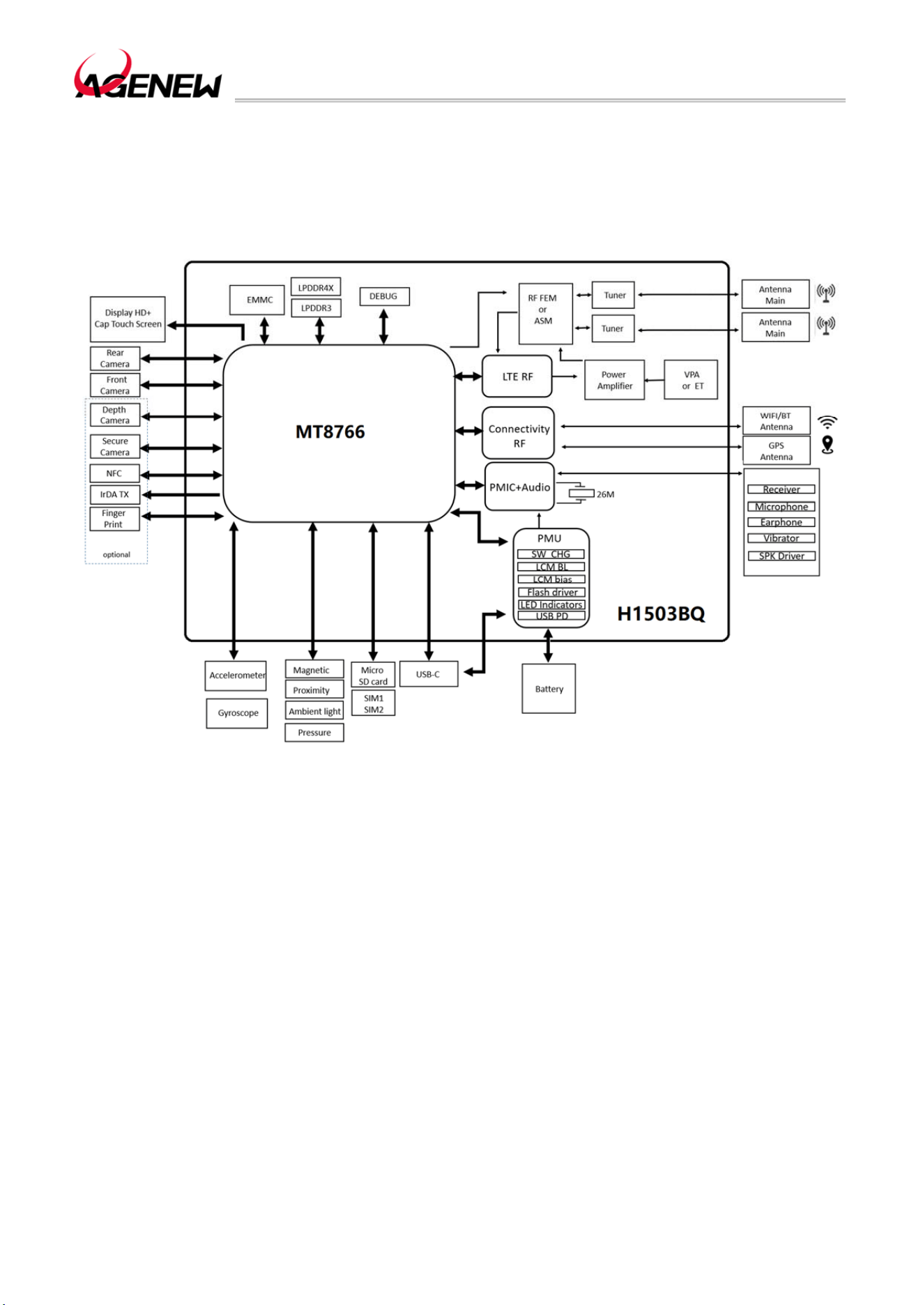
2.3 Functional block diagram
The following diagram shows the H1503BQ functional block diagram.
Figure 1 Functional Block Diagram

H1503BQ_Hardware Design Guide
WWW.AGENEWTECH.COM
11
3 Application Interfaces
3.1 Overview
The H1503BQ module is available in an LCC+LGA package with a total of 275 pins. The
following chapters elaborate on the functions of each set of interfaces of the module:
⚫Power supply
⚫Power on and off
⚫VRTC interface
⚫Charging port
⚫USB interface
⚫UART interface
⚫SIM interface
⚫SD card interface
⚫GPIO interface
⚫I2C interface
⚫I2S interface
⚫SPI interface
⚫ADC interface
⚫Motor drive interface
⚫LCM interface
⚫Touchscreen interface
⚫Camera interface
⚫Sensor interface
⚫Audio interface
⚫Forced download of the interface
⚫LED interface
H1503BQ_Hardware Design Guide
WWW.AGENEWTECH.COM
12
3.2 Pin Assignment
The pinout diagram of the H1503BQ module is as follows:
Figure 2 H1503BQ Pinout Diagram (Top View)
H1503BQ_Hardware Design Guide
WWW.AGENEWTECH.COM
13
3.3 Pin Description
Table 3 I/O Parameter Definition
type description
IO Bi-directional ports
DI Digital inputs
DO Digital output
PI Power input
PO Power output
AI Analog inputs
AO Analog output
OD Open drain
The pin function and electrical characteristics of the H1503BQ are described in the
following table:
Table 4 Pin Description
power supply
Pin Name
Pin
Number
I/O Description
DC
Characteristics
Remark
VBAT 1,2,145,146 PI
Module power
supply
Vmax=4.4V
Vmin=3.4V
Vnorm=3.8V
The power supply must be
able to deliver up to 4A , and
an external EOS device is
recommended
VIO18_PMU 111 PO
System 1.8V I/O
power supply
Vnorm=1.8V
IOmax=600mA
For the voltage domain of
external cameras, LCDs,
sensors, and I/O ports,
1.0uF~2.2uF bypass
capacitors need to be added
when using. The system
power cannot be turned off
VIO28_PMU 156 PO
System 2.8V I/O
power supply
Vnorm=2.8V
IOmax=200mA
To supply power to external
sensors and touch screens,
1.0uF~4.7uF bypass
capacitors need to be added
when used. The system
H1503BQ_Hardware Design Guide
WWW.AGENEWTECH.COM
14
power cannot be turned off
VCAM_AVDD 129 PO
Camera analog
power supply
Vnorm=2.8V
IOmax =200mA
To supply power to the
analog voltage part of the
camera, 1.0uF ~ 4.7uF
bypass capacitor needs to
be added when using. If
you're not using it, turn it off
VCAM_AF 193 PO Output 2.8V
Vnorm=2.8V
IOmax=400mA
To power the focusing
motor of the external
camera, 1.0uF ~ 2.2uF
bypass capacitors need to
be added when using. If
you're not using it, turn it off
VCAMD_PMU 192 PO
Digital power
supply for the
camera
Vnorm=1.2V
IOmax=400mA
To supply power to the
digital voltage part of the
camera, a bypass capacitor
of 1.0uF ~ 2.2uF needs to
be added when using. If
you're not using it, turn it off
VCAM_IOVDD 125 PO
Camera IO power
supply
Vnorm=1.8V
IOmax=300mA
To supply power to the I/O
part of the camera, a
bypass capacitor of
1.0uF~2.2uF needs to be
added when using. If you're
not using it, turn it off
VRTC 126 PIO
RTC clock power
supply
Vnorm=2.8V
VOmax=2.98V
GND
3,7,12,15,27,51,62,69,76,78,85,86,88,89,120,122,130,132,135,140,143,144,162,171,172,
176,189~191,202,203,204,206~224,226~231,233~238,240,241,243~245,247,248,250,
251,255,256,258,259,261,266,268,269,271~274
Audio Interface
Pin name
Pin
number
I/O Description
DC
Characteristics
Remark
MICBIAS0 147 PO
MIC0, MIC2 bias
voltage
VO=0V~2.94V
MIC0_P 4 AI
The main microphone
input is positive
MIC0_N 5 AI
The main microphone
input is negative
MIC2_P 148 AI
The secondary
microphone input is
positive
MIC2_N 149 AI
The negative pole of
the secondary
microphone input
EAR_P 8 AO
Differential handset
output positive
EAR_N 9 AO
Differential earpiece
outputs a negative pole
LINEOUT_P 10 AO
Differential line out
output positive
H1503BQ_Hardware Design Guide
WWW.AGENEWTECH.COM
15
LINEOUT_N 11 AO
Differential line out
output negetive
MICBIAS1 155 PO
Headphone MIC bias
voltage
VO=0V~2.94V
HP_MIC 6 AI Headphone MIC input
AU_HPR 136 AO
The right channel of
the headphones
AU_REFN 137 AI
Headset reference
ground
If not, it needs to be
grounded
AU_HPL 138 AO
Headphone left
channel
HP_DET 139 AI
Headphone insertion
detection
USB Interface
Pin Name
Pin
Number
I/O Description
DC
Characteristics
Remark
VBUS 141,142 PI
Charging power input;
USB/adapter insertion
detection
Vmax=14V
Vmin=4V
Vnorm=5.0V
Test points must be
reserved
USB_DM 13 IO
USB 2.0 differential
data negative
USB 2.0
compliant
specification
A differential
impedance of 90Ω is
required
Test points must be
reserved
USB_DP 14 IO
USB 2.0 differential
data positive
USB_ID 16 DI
USB ID detection
signal
(U) SIM Interface
Pin Name
Pin
Number
I/O Description
DC
Characteristics
Remark
USIM1_VDD 26 PO (U) SIM1 power supply
Vmax=3V
Vnorm=1.8V
Automatic identification
of modules: 1.8V or 3V
(U)SIM Card
USIM1_DET 22 DI
(U) SIM1 insertion and
unplugging detection
VOLmax=0.45V
VOHmin=1.35V
If not, suspend
USIM1_RST 23 DO (U) SIM1 reset signal
VOLmax=0.4V
VOHmin=1.62V
USIM1_CLK 24 DO (U) SIM1 clock signal
VOLmax=0.4V
VOHmin=1.62V
USIM1_DATA 25 IO (U) SIM data signal
VILmax=0.27V
VIHmin=1.4V
VOLmax=0.36V
VOHmin=1.4V
USIM2_VDD 21 PO (U) SIM2 power supply
Vmax=3V
Vnorm=1.8V
模块自动识别 1.8V 或
3V (U)SIM 卡
USIM2_DET 17 DI
(U) SIM2 insertion and
unplugging detection
VOLmax=0.45V
VOHmin=1.35V
If not, suspend
USIM2_RST 18 DO (U) SIM2 reset signal
VOLmax=0.4V
VOHmin=1.62V
H1503BQ_Hardware Design Guide
WWW.AGENEWTECH.COM
16
USIM2_CLK 19 DO (U) SIM2 clock signal
VOLmax=0.4V
VOHmin=1.62V
USIM2_DATA 20 IO (U) SIM2 data signal
VILmax=0.27V
VIHmin=1.4V
VOLmax=0.36V
VOHmin=1.4V
SD Card Interface
Pin Name
Pin
Number
I/O Description
DC
Characteristics
Remark
SD_CLK 39 DO
SD card high-speed
digital clock
VOLmax=0.41V
VOHmin=2.1V
SD_CMD 40 DO SD card control signal
VILmax=0.85V
VIHmin=1.75V
VOLmax=0.41V
VOHmin=2.1V
SD_DATA0 41 IO
High-speed
bidirectional digital
signal
VILmax=0.85V
VIHmin=1.75V
VOLmax=0.41V
VOHmin=2.1V
SD_DATA1 42 IO
SD_DATA2 43 IO
SD_DATA3 44 IO
SD_DET 45 DI
SD card CPU status
detection
VILmax=0.63V
VIHmin=1.17V
If not, suspend
SD_VDD 38 PO SD card power supply
Vnorm=3.0V
IOmax=800mA
Touchscreen Interface
Pin Name
Pin
Number
I/O Description
DC
Characteristics
Remark
TP_RST 31 DO
Touch screen reset
signal
VOLmax=0.45V
VOHmin=1.35V
1.8V voltage domain
Valid low
TP_INT 30 DI
The touch screen
interrupts the signal
VOLmax=0.45V
VOHmin=1.35V
1.8V voltage domain
SCL0 47 DO Touchscreen I2C clock
VOLmax=0.45V
VOHmin=1.35V
No external pull-up is
required
SDA0 48 IO Touchscreen I2C data
VOLmax=0.45V
VOHmin=1.35V
No external pull-up is
required
LCM Interface
Pin Name
Pin
Number
I/O Description
DC
Characteristics
Remark
DISP_PWM 29 DO PWM output
VOLmax=0.45V
VOHmin=1.35V
Adjust the brightness
of the backlight
LCD_RST 49 DO LCD reset signal
VOLmax=0.45V
VOHmin=1.35V
1.8V voltage domain
Valid low
DSI_TE 50 DO
LCD tearing effect
signal
VOLmax=0.45V
VOHmin=1.35V
1.8V voltage domain
DSI_CKP 53 AO
LCD MIPI clock
positive

H1503BQ_Hardware Design Guide
WWW.AGENEWTECH.COM
17
DSI_CKN 52 AO
LCD MIPI clock
negative
DSI_D0P 55 AO
The LCD MIPI data 0
positive
DSI_D0N 54 AO
The LCD MIPI data 0
negative
DSI_D1P 57 AO
LCD MIPI data 1
positive
DSI_D1N 56 AO
The LCD MIPI data 1
negative
DSI_D2P 59 AO
The LCD MIPI data
positive
DSI_D2N 58 AO
LCD MIPI data
negative 2
DSI_D3P 61 AO
The LCD MIPI data 3
positive
DSI_D3N 60 AO
The LCD MIPI data 3
negative
Camera Interface
Pin Name
Pin
Number
I/O Description
DC
Characteristics
Remark
CSI0_CLKN 157 AO
MIPI CSI0 clock
negative
CSI0_CLKP 196 AO
MIPI CSI0 clock
positive
CSI0_LN0N 158 AI
MIPI CSI0 data 0
negative
CSI0_LN0P 197 AI
MIPI CSI0 data 0
positive
CSI0_LN1N 159 AI
MIPI CSI0 data 1
negative
CSI0_LN1P 198 AI
MIPI CSI0 data 1
positive
CSI0_LN2N 160 AI
MIPI CSI0 data 2
negative
CSI0_LN2P 199 AI
MIPI CSI0 data 2
positive
CSI0_LN3N 161 AI
MIPI CSI0 data 3
negative
CSI0_LN3P 200 AI
MIPI CSI0 data 3
positive
CSI1_CLKN 63 AO
MIPI CSI0 clock
negative
CSI1_CLKP 64 AO
MIPI CSI0 clock
positive
CSI1_LN0N 65 AI
MIPI CSI0 data 0
negative
CSI1_LN0P 66 AI
MIPI CSI0 data 0
positive
H1503BQ_Hardware Design Guide
WWW.AGENEWTECH.COM
18
CSI1_LN1N 67 AI
MIPI CSI0 data 1
negative
CSI1_LN1P 68 AI
MIPI CSI0 data 1
positive
CSI1_LN2N 72 AI
MIPI CSI0 data 2
negative
CSI1_LN2P 73 AI
MIPI CSI0 data 2
positive
CSI1_LN3N 70 AI
MIPI CSI0 data 3
negative
CSI1_LN3P 71 AI
MIPI CSI0 data 3
positive
CAM0_MCLK 74 DO
The camera 0 clock
signal
VOLmax=0.45V
VOHmin=1.35V
1.8V voltage domain
CAM1_MCLK 75 DO Camera 1 clock signal
VOLmax=0.45V
VOHmin=1.35V
1.8V voltage domain
CAM0_RST 79 DO Camera 0 reset signal
VOLmax=0.45V
VOHmin=1.35V
CAM0_PDN 80 DO
Camera 1 shut down
signal
VOLmax=0.45V
VOHmin=1.35V
CAM1_RST 81 DO Camera 0 reset signal
VOLmax=0.45V
VOHmin=1.35V
CAM1_PDN 82 DO
Camera 1 shut down
signal
VOLmax=0.45V
VOHmin=1.35V
SCL2 166 DO
Camera I2C clock
signal
VOLmax=0.45V
VOHmin=1.35V
No external pull-up is
required
SDA2 205 IO
Camera I2C data
signal
VOLmax=0.45V
VOHmin=1.35V
No external pull-up is
required
Button Interface
Pin Name
Pin
Number
I/O Description
DC
Characteristics
Remark
PWRKEY 114 DI
Power on and off
button
Vmax=0.7*VBAT
Vmin=0.3*VBAT
Valid low
VOL+ 95 DI Volume up
VOLmax=0.45V
VOHmin=1.35V
If not, suspend
THEFT- 96 DI
Volume reduction and
forced downloads
VOLmax=0.45V
VOHmin=1.35V
If not, suspend
SYSRSTB 225 DI Module reset
VOLmax=0.45V
VOHmin=1.35V
If not, suspend
UART Interface
Pin Name
Pin
Number
I/O Description
DC
Characteristics
Remark
UART0_RXD 94 DO Debug UART send
VOLmax=0.45V
VOHmin=1.35V
1.8V voltage domain,
If not, it will be
suspended
UART0_TXD 93 DI Debug UART reception
VILmax=0.63V
VIHmin=1.17V
UART1_TXD 34 DO UART1
VOLmax=0.45V
VOHmin=1.35V
1.8V voltage domain,
If not, it will be
suspended

H1503BQ_Hardware Design Guide
WWW.AGENEWTECH.COM
19
UART1_RXD 35 DI UART1 receives
VILmax=0.63V
VIHmin=1.17V
UART1_CTS 36 DO Clear Send to Module
UART1_RTS 37 DI Module request sends
I2C Interface
Pin Name
Pin
Number
I/O Description
DC
Characteristics
Remark
SCL1 91 DO I2C1 serial clock
VOLmax=0.45V
VOHmin=1.35V
No external pull-up is
required
SDA1 92 IO I2C1 serial data
VOLmax=0.45V
VOHmin=1.35V
No external pull-up is
required
SCL2 166 DO I2C2 serial clock
VOLmax=0.45V
VOHmin=1.35V
No external pull-up is
required
SDA2 205 IO I2C2 serial data
VOLmax=0.45V
VOHmin=1.35V
No external pull-up is
required
SCL3 167 DO I2C3 serial clock
VOLmax=0.45V
VOHmin=1.35V
No external pull-up is
required
SDA3 168 IO I2C3 serial data
VOLmax=0.45V
VOHmin=1.35V
No external pull-up is
required
SCL4 169 DO I2C4 serial clock
VOLmax=0.45V
VOHmin=1.35V
No external pull-up is
required
SDA4 170 IO I2C4 serial data
VOLmax=0.45V
VOHmin=1.35V
No external pull-up is
required
SCL5 83 DO I2C5 serial clock
VOLmax=0.45V
VOHmin=1.35V
No external pull-up is
required
SDA5 84 IO I2C5 serial data
VOLmax=0.45V
VOHmin=1.35V
No external pull-up is
required
SPI Interface
Pin Name
Pin
Number
I/O Description
DC
Characteristics
Remark
SPI0_CSB 117 DO Chip selection signal
VOLmax=0.45V
VOHmin=1.35V
SPI0_CLK 116 DO Clock signals
VOLmax=0.45V
VOHmin=1.35V
SPI0_MO 118 DO Data output
VOLmax=0.45V
VOHmin=1.35V
SPI0_MI 119 DI Data input
VILmax=0.63V
VIHmin=1.17V
SPI1_CSB 107 DO Chip selection signal
VOLmax=0.45V
VOHmin=1.35V
Reuse I2S1_BCK
SPI1_CLK 108 DO Clock signals
VOLmax=0.45V
VOHmin=1.35V
Reuse I2S1_DO
SPI1_MO 109 DO Data output
VOLmax=0.45V
VOHmin=1.35V
Reuse I2S1_LRCK
SPI1_MI 110 DI Data input
VILmax=0.63V
VIHmin=1.17V
Reuse I2S1_MCK
H1503BQ_Hardware Design Guide
WWW.AGENEWTECH.COM
20
SPI2_CSB 103 DO Chip selection signal
VOLmax=0.45V
VOHmin=1.35V
SPI2_CLK 104 DO Clock signals
VOLmax=0.45V
VOHmin=1.35V
SPI2_MO 105 DO Data output
VOLmax=0.45V
VOHmin=1.35V
SPI2_MI 106 DI Data input
VILmax=0.63V
VIHmin=1.17V
SPI3_CSB 99 DO Chip selection signal
VOLmax=0.45V
VOHmin=1.35V
Reuse I2S2_BCK
SPI3_CLK 100 DO Clock signals
VOLmax=0.45V
VOHmin=1.35V
Reuse I2S2_DO
SPI3_MO 101 DO Data output
VOLmax=0.45V
VOHmin=1.35V
Reuse I2S2_LRCK
SPI3_MI 102 DI Data input
VILmax=0.63V
VIHmin=1.17V
Reuse I2S2_MCK
SPI4_CSB 242 DO Chip selection signal
VOLmax=0.45V
VOHmin=1.35V
SPI4_CLK 270 DO Clock signal
VOLmax=0.45V
VOHmin=1.35V
SPI4_MO 264 DO Data output
VOLmax=0.45V
VOHmin=1.35V
SPI4_MI 265 DI Data input
VILmax=0.63V
VIHmin=1.17V
Battery Interface
Pin Name
Pin
Number
I/O Description
Dc
Characteristics
Remark
BAT_P 133 AI
Battery voltage
detection
CS_P 188 AI
Battery Current
Detection+
Ground when not in
use
CS_N 187 AI
Battery Current
Detection-
Ground when not in
use
ADC_IN3 185 AI Battery type detection
General-purpose ADC
interface
VBAT_THERM 134 AI
Battery temperature
detection
Antenna Interface
Pin Name
Pin
Number
I/O Description
DC
Characteristics
Remark
ANT_MAIN 87 IO Main antenna interface
50Ω characteristic
impedance
ANT_DRX 131 AI
LTE diversity antenna
interface
50Ω characteristic
impedance
ANT_WIFI/BT 77 AIO
Wi-Fi 2.4G/Wi-Fi 5G/BT
antenna interface
50Ω characteristic
impedance
Default WIFI/BT/GNSS
3in1 antenna
ANT_GNSS 121 AI GPS antenna interface
50Ω characteristic
impedance
H1503BQ_Hardware Design Guide
WWW.AGENEWTECH.COM
21
Default NC
BPI_BUS5 260 DO
Antenna Tuner switch
control
For antenna tuning
control only
BPI_BUS6 262 DO
Antenna Tuner switch
control
For antenna tuning
control only
BPI_BUS7 173 DO
Antenna Tuner switch
control
For antenna tuning
control only
Motor Drive Interface
Pin Name
Pin
Number
I/O Description
DC
Characteristics
Remark
VIBR_DRV 28 PO
Vibration motor power
output
Vmax=3.3V
Vmin=1.2V
Vnorm=2.8V
Imax=200mA
Leds Indicate The Interface
Pin Name
Pin
Number
I/O Description
DC
Characteristics
Remark
CHG_LED 195 AI Charging indication
Input Current Range:
1mA~6mA
LED_R 252 AI LED control negative
The detached version
is GPIO174
LED_G 253 AI LED control negative
The detached version
is GPIO173
LED_B 249 AI LED control negative
The detached version
is GPIO175
ADC Interface
Pin Name
Pin
Number
I/O Description
DC
Characteristics
Remark
ADC_IN2 128 AI
ADC analog sampling
input
If not, it will be
grounded
Other Interfaces
Pin Name
Pin
Number
I/O Description
DC
Characteristics
Remark
USB_BOOT 46 DI
Force the module into
download mode
Enter high to enter
upgrade mode
FLASH_LED 180 AO Flash positive output Iomax=1A
NFC_CLK 181 DO NFC clock
GPIO_GPS
_LNA_EN
194 DO
External GPS LNA
enables control
GPIO Interface
Pin Name
Pin
Number
I/O Description
DC
Characteristics
Remark
GPIO6 33 IO GPIO
VOLmax=0.45V
VOHmin=1.35V
Multiplex EINT6

H1503BQ_Hardware Design Guide
WWW.AGENEWTECH.COM
22
GPIO89 90 IO GPIO
VOLmax=0.45V
VOHmin=1.35V
GPIO10 97 IO GPIO
VOLmax=0.45V
VOHmin=1.35V
Multiplex EINT10
GPIO9 98 IO GPIO
VOLmax=0.45V
VOHmin=1.35V
Multiplex EINT9
GPIO150 112 IO GPIO
VOLmax=0.45V
VOHmin=1.35V
GPIO151 113 IO GPIO
VOLmax=0.45V
VOHmin=1.35V
GPIO3 115 IO GPIO
VOLmax=0.45V
VOHmin=1.35V
Multiplex EINT3
GPIO88 123 IO GPIO
VOLmax=0.45V
VOHmin=1.35V
GPIO160 124 IO GPIO
VOLmax=0.45V
VOHmin=1.35V
GPIO87 127 IO GPIO
VOLmax=0.45V
VOHmin=1.35V
GPIO7 153 IO GPIO
VOLmax=0.45V
VOHmin=1.35V
Multiplex EINT7
GPIO8 154 IO GPIO
VOLmax=0.45V
VOHmin=1.35V
Multiplex EINT8
GPIO107 163 IO GPIO
VOLmax=0.45V
VOHmin=1.35V
GPIO109 164 IO GPIO
VOLmax=0.45V
VOHmin=1.35V
GPIO108 165 IO GPIO
VOLmax=0.45V
VOHmin=1.35V
GPIO165 177 IO GPIO
VOLmax=0.45V
VOHmin=1.35V
GPIO176 178 IO GPIO
VOLmax=0.45V
VOHmin=1.35V
GPIO167 179 IO GPIO
VOLmax=0.45V
VOHmin=1.35V
GPIO166 182 PO GPIO
VOLmax=0.45V
VOHmin=1.35V
GPIO172 186 IO GPIO
VOLmax=0.45V
VOHmin=1.35V
GPIO168 201 DO GPIO
VOLmax=0.45V
VOHmin=1.35V
GPIO164 232 DO GPIO
VOLmax=0.45V
VOHmin=1.35V
GPIO169 239 DI GPIO
VOLmax=0.45V
VOHmin=1.35V
GPIO152 267 IO GPIO
VOLmax=0.45V
VOHmin=1.35V
H1503BQ_Hardware Design Guide
WWW.AGENEWTECH.COM
23
3.4 Power Supply
H1503BQ provides 4 VBAT pins for connecting an external battery to power the module.
The VBAT supply voltage input range is 34V~4.4V, the recommended value is 3.8V. The
performance of the VBAT power supply, such as load capacity, ripple size, etc., will directly
affect the performance and stability of the module. In extreme cases, the current consumption
of the module may reach an instantaneous peak of about 4A, and if the power supply capacity
is insufficient, the voltage will drop. If the voltage drops to 3If the module is less than 1V, it will
cause the module to power off and shut down.
In order to ensure that the VBAT voltage does not drop below 3.1V, it is recommended to
connect a 22uF (0603 package) and 2.2UF (0402 package) and 100nF and 33pF (0201
package) filter capacitors, and it is recommended that the PCB traces of VBAT be as short
and wide as possible, and the width of VBAT traces is not less than 3mm; And the longer the
trace, the wider the line width; The ground plane of the power supply section should be as
complete as possible.
In order to suppress the impact of power supply fluctuations and ensure the stability of
the output power supply, it is recommended to add a surge tube at the front end of the power
supply and place it close to the VBAT of the module to play the role of surge protection.
Figure 3 VBAT Input Reference Circuit
Remark
1. When the module cannot be shut down normally due to abnormality, it is recommended
to disconnect the power supply to turn off the module, and then power on again to restart the
module.
2. When the power drops to 0%, the system will trigger an automatic shutdown; Therefore,
the power supply design should be consistent with the drive configuration of the fuel gauge.
H1503BQ_Hardware Design Guide
WWW.AGENEWTECH.COM
24
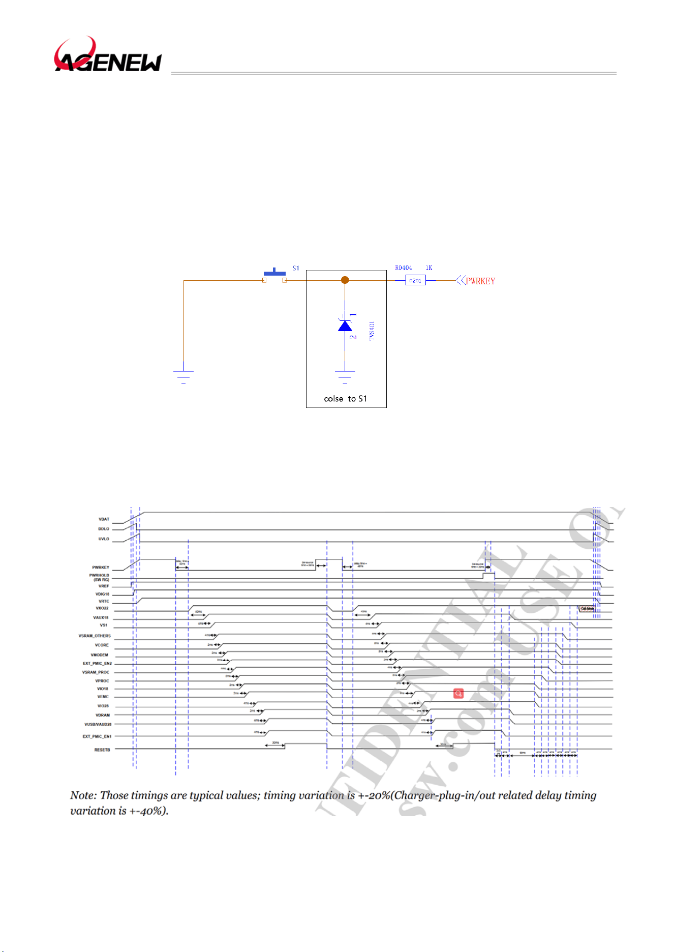
3.5 Power On and Off
3.5.1 Power On
After the VBAT is powered on, the module can be powered on by pulling the PWRKEY
down for at least 2s.
N TVS is need to be placed near the button for ESD protection and connect a 1K resistor
in series to the PWRKEY. The reference circuit is as follows:
Figure 4 The Open-Set Drive Refers To The Boot Circuit
The boot sequence diagram is shown in the following figure:
Figure 5 Boot Sequence Diagram
H1503BQ_Hardware Design Guide
WWW.AGENEWTECH.COM
25
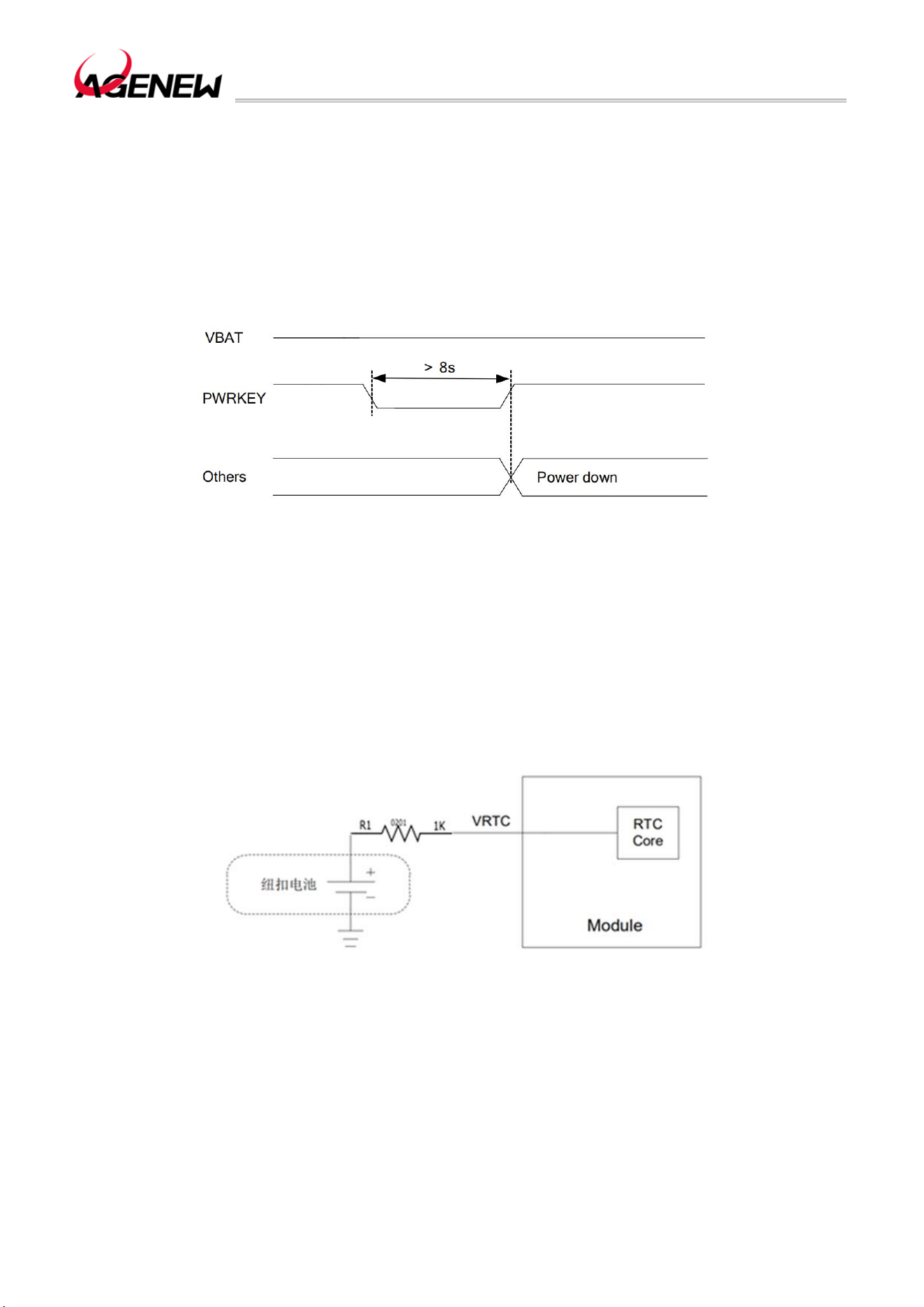
3.5.2 Power Off
Module shutdown can be achieved by pulling the PWRKEY down for at least 1 second.
After the module detects the shutdown action, a prompt window will pop up on the screen to
confirm whether to continue the shutdown action.
It is also possible to force a shutdown by pulling down the PWRKEY for a long time
(minimum 8s). The forced shutdown sequence diagram is shown below
Figure 6 Sequence Diagram of Forced Shutdown
3.6 VRTC Interface
VRTC is the external power pin of the RTC inside the module. When the VBAT is
disconnected and the user needs to save the real-time clock, the VRTC pin cannot be left
empty and can be powered by connecting an external battery to the VRTC pin. When the
RTC power supply is powered by an external battery, the reference circuit is as follows:
Figure 7 A Rechargeable Coin Cell Battery Powers The RTC
If the RTC fails, the module can be time-synchronized over the network after powering
on.
⚫ The input voltage range of VRTC power supply is 0V~2.98V2.8V typical.
⚫ When powered by VBAT, the RTC error is 50ppm. When VRTC is powered, the RTC
error is 200ppm.

H1503BQ_Hardware Design Guide
WWW.AGENEWTECH.COM
26
⚫ When an external rechargeable coin cell battery is required, the ESR of the coin cell
battery must be less than 2K. Recommend the MS621FE FL11E by SEIKO.
3.7 Power Output
H1503BQ Multiple power outputs for peripheral circuitry.
Table 5 Power Supply Description
Power Supply
Pin Name
Pin
Number
I/O Description
DC
Characteristics
Remark
VBAT 1,2,145,146 PI
Module power
supply
Vmax=4.4V
Vmin=3.4V
Vnorm=3.8V
The power supply must
be able to deliver up to
4A , and an external
EOS device is
recommended
VIO18_PMU 111 PO
System 1.8V I/O
power supply
Vnorm=1.8V
IOmax=600mA
For the voltage domain
of external cameras,
LCDs, sensors, and I/O
ports, 1.0uF~2.2uF
bypass capacitors
need to be added
when using. The
system power cannot
be turned off
VIO28_PMU 156 PO
System 2.8V I/O
power supply
Vnorm=2.8V
IOmax=200mA
To supply power to
external sensors and
touch screens,
1.0uF~4.7uF bypass
capacitors need to be
added when used. The
system power cannot
be turned off
VCAM_AVDD 129 PO
Camera analog
power supply
Vnorm=2.8V
IOmax =200mA
To supply power to the
analog voltage part of
the camera, 1.0uF ~
4.7uF bypass capacitor
needs to be added
when using. If you're
not using it, turn it off
VCAM_AF 193 PO Output 2.8V
Vnorm=2.8V
IOmax=400mA
To power the focusing
motor of the external
camera, 1.0uF ~ 2.2uF
bypass capacitors
need to be added
when using. If you're
not using it, turn it off
VCAMD_PMU 192 PO
Digital power supply
for the camera
Vnorm=1.2V
IOmax=400mA
To supply power to the
digital voltage part of
the camera, a bypass
capacitor of 1.0uF ~
2.2uF needs to be
added when using. If

H1503BQ_Hardware Design Guide
WWW.AGENEWTECH.COM
27
you're not using it, turn
it off
VCAM_IOVDD 125 PO
Camera IO power
supply
Vnorm=1.8V
IOmax=300mA
To supply power to the
I/O part of the camera,
a bypass capacitor of
1.0uF~2.2uF needs to
be added when using.
If you're not using it,
turn it off
KINDERGART
EN
126 PIO
RTC clock power
supply
Vnorm=2.8V
VOmax=2.98V
USIM1_VDD 26 PO
(U) SIM1 power
supply
Vmax=3V
Vnorm=1.8V
The module
automatically
recognizes the 1.8V or
3V (U) SIM card
USIM2_VDD 21 PO
(U) SIM2 power
supply
Vmax=3V
Vnorm=1.8V
The module
automatically
recognizes the 1.8V or
3V (U) SIM card
SD_VDD 38 PO
SD card power
supply
Vnorm=3.0V
IOmax=800mA
VIBR_DRV 28 PO
Vibration motor
power output
Vmax=3.3V
Vmin=1.2V
Vnorm=2.8V
Imax=200mA
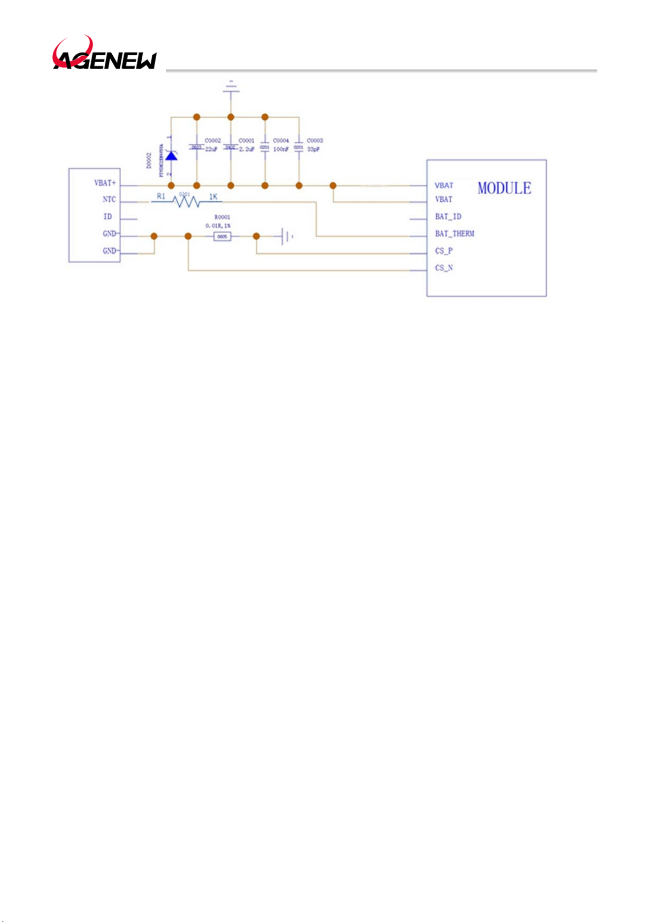
3.8 Charging and battery management
The H1503BQ module features programmable switch-mode lithium battery charging,
capable of charging single lithium and polymer batteries. The charging process includes trickle
charging, pre-charging, constant current charging, constant voltage charging and other states.
⚫ Trickle charging: When the battery voltage is lower than 2.0V, the system is in trickle
charging mode, and the charging current is 100mA, and the current and voltage cannot be
modified by programming in this state.
⚫ Pre-charge: When the battery voltage is between 2.0V~3.5V (programmable cut-off
voltage range: 2.0V~3.5V, default 3.0V), module pre-charge mode, the default charging
current is 150mA (programmable range is charging current: 100mA~850mA, default 150mA).
⚫ Constant current charging: When the battery voltage is between the pre-charge cut-off
voltage and 4.35V (the programmable range of the constant current charge cut-off voltage:
3.6V~4.7V, the default is 4.35V), the module enters the constant current charging mode, and
the charging current software can be set to 500mA~5000mA (the default setting of the
software: USB charging current is 500mA, adapter charging current is 2A).
⚫ Constant Voltage Charging: Constant Voltage Charging: When the battery voltage is
greater than or equal to the constant current charging cut-off voltage (default 4.)35V), start

H1503BQ_Hardware Design Guide
WWW.AGENEWTECH.COM
28
constant voltage charging, charging at this time. The current gradually decreases, and when
the charging current decreases to the charging cut-off current (the programmable range of the
charging cut-off current: 100mA~850mA, the default is 250mA), the charging stops.
⚫ Full charge and recharge: When the battery is fully charged and stops charging, and
the battery voltage is lower than the constant current charge cut-off voltage - recovery charge
voltage (recovery charge voltage programmable range: 100mV~400mV, the default is 100mV),
the system returns to constant current charging mode.
If the product needs to support other charging functions, a charging circuit needs to be
built on the bottom plate.
Table 6 Charging Interface Pin Definition
Battery Interface
Pin Name
Pin
Number
I/O Description
DC
Characteristics
Remark
VBUS 141,142 PI
Charging power input;
USB/adapter insertion
detection
Vmax=14V
Vmin=4V
Vnorm=5.0V
Test points must
be reserved
VBAT 1,2,145,146 PI Module power supply
Vmax=4.4V
Vmin=3.4V
Vnorm=3.8V
The power supply
must be able to
deliver up to 4A ,
and an external
EOS device is
recommended
BAT_P 133 AI Battery voltage detection
CS_P 188 AI
Battery Current
Detection+
Ground when not
in use
CS_N 187 AI Battery Current Detection-
Ground when not
in use
VBAT_THERM 134 AI
Battery temperature
detection
H1503BQ module has battery temperature detection function. The implementation of this
function requires a thermistor to be integrated into the battery (NTC with 10K 1% and B
constant of 3380K is selected by default, SUNLORD's SDNT1005X103F3380FTF is
recommended), and the thermistor needs to be connected to the NTC pin. If the NTC pin is
not connected, it will cause problems such as not turning on, the battery not charging, and the
battery level display incorrectly. The schematic diagram of the battery charging connection is
shown below:
H1503BQ_Hardware Design Guide
WWW.AGENEWTECH.COM
29
Figure 8 Schematic Diagram Of Battery Charging Connection
H1503BQ module has Fuel Gauge function, and It can accurately estimate the real-time
battery charge, which not only protects the battery from over-discharge, but also allows the
user to know exactly how much power is left to estimate how long it can be used, and save
important data in time.
Mobile devices such as handheld devices and handheld POS machines are battery-
powered. For different types of batteries, it is necessary to modify the charge and discharge
curves of the battery in the software to achieve the best application effect.
If the customer is using a battery that does not have a thermistor, or if the customer is
using a power adapter to power the module, only VBAT and GND need to be connected. In
this case, in order to prevent the system from misjudging that the battery does not exist and
cannot be turned on, the customer should connect the NTC pin to GND through a 10KΩ
resistor. The VBAT_SNS pins must be connected properly, otherwise the normal use of the
module will be affected. CS_P and CS_N are used to detect battery charge and discharge
currents, and the internal current detection mechanism is currently used by default.
3.9 USB Interface
H1503BQ provides a USB port that complies with the USB 2.0 specification and supports
up to 480Mbps. The USB interface can be used for AT instruction transfer, data transfer,
software debugging and software upgrade.
The following table shows the pin definitions for the USB interface:
H1503BQ_Hardware Design Guide
WWW.AGENEWTECH.COM
30
Table 7 USB Interface Pin Definition
USB Interface
Pin Name
Pin
Number
I/O Description
DC
Characterist
ics
Remark
VBUS 141,142 PI
Charging power input
USB/adapter insertion
detection
Vmax=14V
Vmin=4V
Vnorm=5.0V
Test points must
be reserved
USB_DM 13 IO
USB 2.0 differential data
negative
USB 2.0
compliant
specification
Require a
differential
impedance of 90Ω
Test points must
be reserved
USB_DP 14 IO
USB 2.0 differential data
positive
USB 2.0
compliant
Require a
differential
impedance of 90Ω
USB_ID 16 DI USB ID detection signal
The USB_VBUS serves as the power input for USB or adapter charging, allowing the
battery to be charged through the charging circuit on the motherboard, and it can also be used
for USB insertion detection. The input voltage range for the power supply is 4.0V to 14.0V,
with a recommended value of 5.0V. Additionally, in the Micro-USB scheme, OTG devices
differentiate using the USB_ID pin. When the USB_ID is floating (default is high level), the
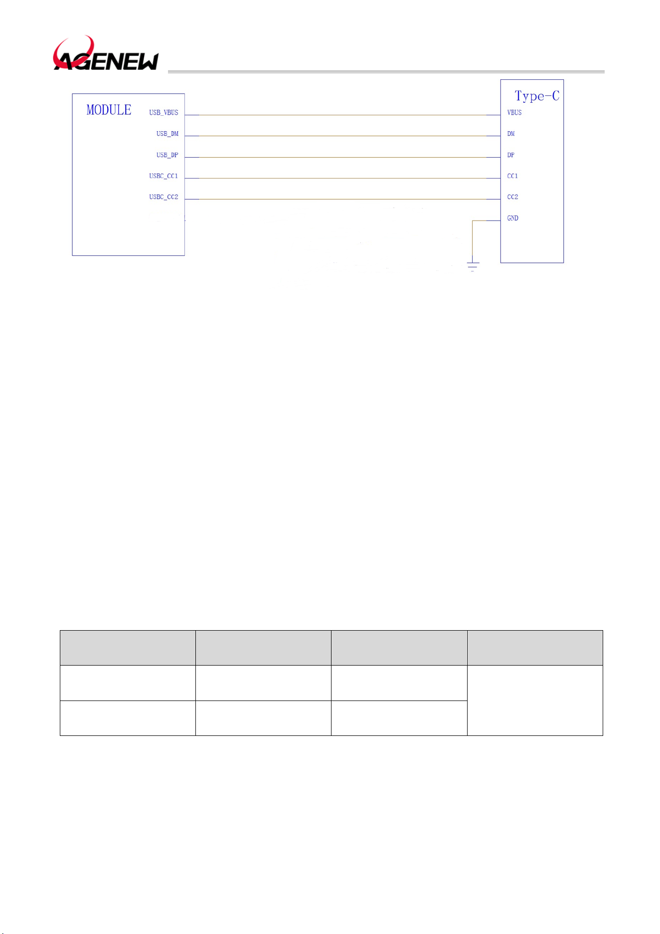
H1503BQ operates in USB Device mode. When the USB_ID is grounded, the H1503BQ
operates in USB HOST mode. If a Type-C interface is required, the user needs to add a CC
protocol chip on the motherboard.
Figure 9 Mirco-USB Interface Reference Design
H1503BQ_Hardware Design Guide
WWW.AGENEWTECH.COM
31
Figure 10 USB Type-C Reference Design
In the circuit design of the USB interface, in order to ensure the performance of the USB,
the following design principles are recommended in the circuit design:
⚫ Envelope processing is required around the USB data cable, using a 90Ω impedance
differential line.
⚫ Reserve ESD protection devices near the USB interface, and place the ESD devices
as close to the USB interface as possible. USB 2.0 ESD protection devices must not exceed
2pF in parasitic capacitance.
⚫ Do not run the USB cable under crystal oscillators, oscillators, magnetic devices, and
RF signals. It is recommended to use inner layers and three-dimensional floors.
Layout cabling requirements: USB 2.0 differential signal cables must be equal in length,
the total length difference of differential signal cables must not exceed 8 inches, and there can
only be two vias/layer variations at most.
Table 8 The Length Of The USB Trace Inside The Module
Pin Number Signal Length (mm)
Length Difference
(mm)
13 USB_DM 23.24696
0.15025
14 USB_DP 23.39721
3.10 UART Interface
The H1503BQ module provides the following 2 sets of UART interfaces:
⚫ UART0: 2-wire serial port, used for debugging by default.
H1503BQ_Hardware Design Guide
WWW.AGENEWTECH.COM
32
⚫ UART1: 4-wire serial port.
UART interface pins are defined in the following table:
Table 9 UART interface pin definition
UART interface
Pin name
Pin
number
I/O description
DC
characteristics
remark
UART0_RXD 94 DO Debug UART send
VOLmax=0.45V
VOHmin=1.35V
1.8V voltage
domain,
If not, suspend
1.8V voltage
domain,
If not, suspend
UART0_TXD 93 DI
Debug UART
receive
VILmax=0.63V
VIHmin=1.17V
UART1_TXD 34 DO UART1 send
VOLmax=0.45V
VOHmin=1.35V
UART1_RXD 35 DI UART1 receive
VILmax=0.63V
VIHmin=1.17V
UART1_CTS 36 DO
Clear Send to
Module
UART1_RTS 37 DI
Module request
send
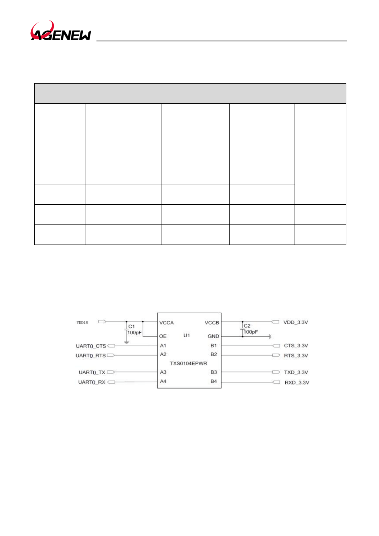
UART1 is a 4-wire serial port with a serial voltage range of 1.8V. When communicating
with a 3.3V serial port, a level shifting chip needs to be added in the middle. The corresponding
reference design is shown in the following figure:
11 Level Translation Reference Circuit (UART1)
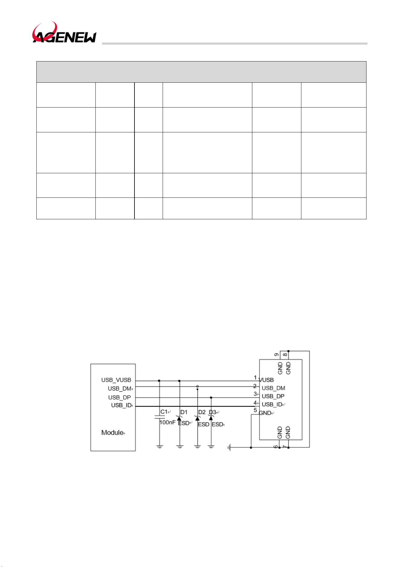
3.11 SIM Interface
H1503BQ There are two SIM ports, which support dual SIM dual standby function (the
software supports it by default).

H1503BQ_Hardware Design Guide
WWW.AGENEWTECH.COM
33
Table 10 SIM Interface Pin Definition
UART Interface
Pin Name
Pin
Number
I/O Description DC Characteristics Remark
USIM1_VDD 26 PO (U) SIM1 power supply
Vmax=3V
Vnorm=1.8V
The module
automatically
recognizes the
1.8V or 3V (U)
SIM card
USIM1_DET 22 DI
(U) SIM1 insertion and
unplugging detection
VOLmax=0.45V
VOHmin=1.35V
If not, suspend
USIM1_RST 23 DO (U) SIM1 reset signal
VOLmax=0.4V
VOHmin=1.62V
USIM1_CLK 24 DO (U) SIM1 clock signal
VOLmax=0.4V
VOHmin=1.62V
USIM1_DATA 25 IO (U) SIM data signal
VILmax=0.27V
VIHmin=1.4V
VOLmax=0.36V
VOHmin=1.4V
USIM2_VDD 21 PO (U) SIM2 power supply
Vmax=3V
Vnorm=1.8V
The module
automatically
recognizes the
1.8V or 3V (U)
SIM card
USIM2_DET 17 DI
(U) SIM2 insertion and
unplugging detection
VOLmax=0.45V
VOHmin=1.35V
If not, suspend
USIM2_RST 18 DO (U) SIM2 reset signal
VOLmax=0.4V
VOHmin=1.62V
USIM2_CLK 19 DO (U) SIM2 clock signal
VOLmax=0.4V
VOHmin=1.62V
USIM2_DATA 20 IO (U) SIM2 data signal
VILmax=0.27V
VIHmin=1.4V
VOLmax=0.36V
VOHmin=1.4V
Through the USIM1_DET pin, the H1503BQ supports SIM card hot-swap function (off by
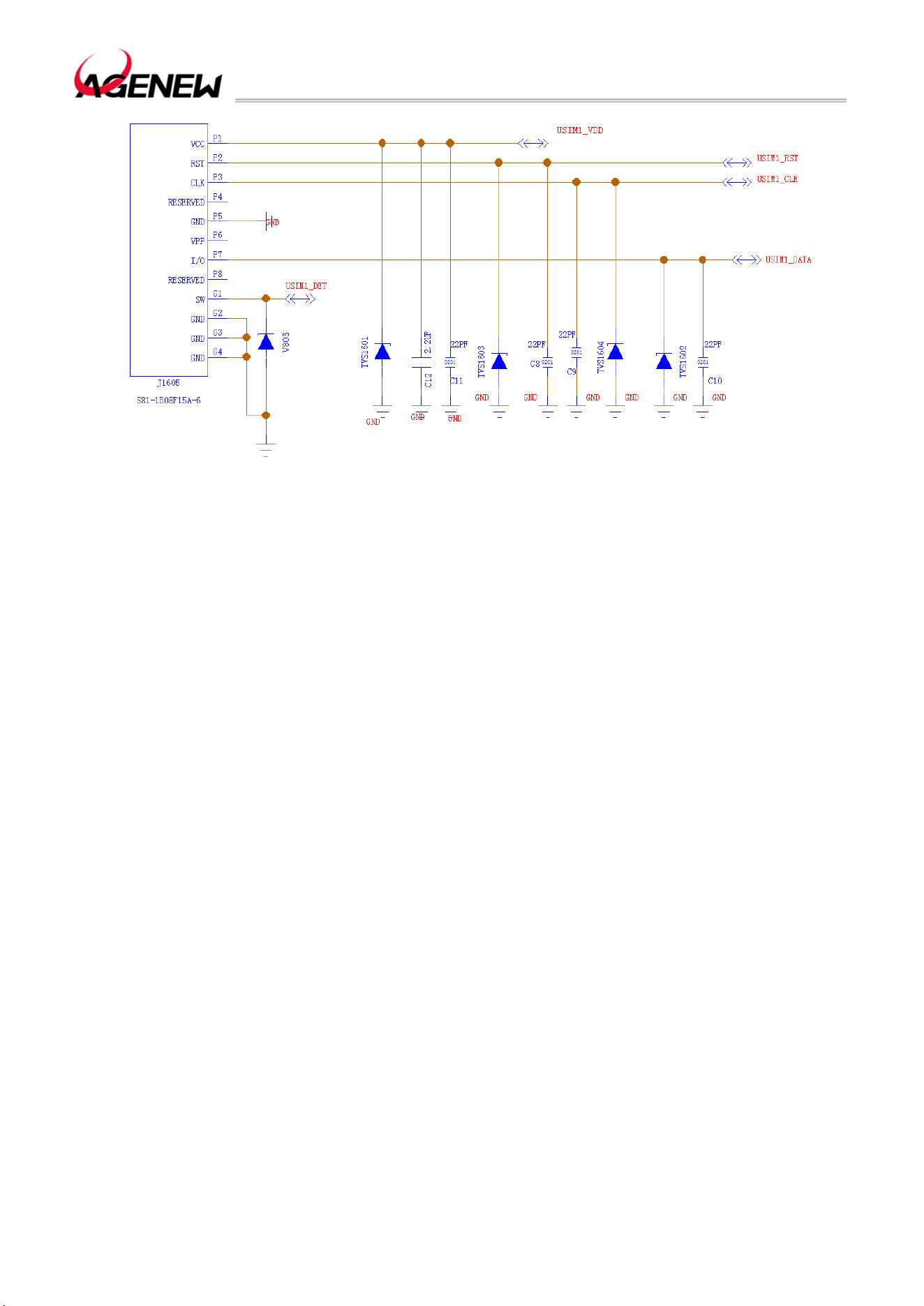
default, can be turned on by software). The reference circuit for the 8-pin SIM interface is as
follows:
H1503BQ_Hardware Design Guide
WWW.AGENEWTECH.COM
34
12 8-pin SIM Reference Circuit
Remark
If it is not necessary to support SIM card hot swapping, the USIM1_DET in the reference
circuit can be floated. The reference circuit of SIM2 is also the same as that of SIM1.
In the circuit design of SIM interface, in order to ensure the good performance and
reliability of the SIM card, the following principles are recommended to be followed in the
circuit design:
⚫ The SIM card signal line is far away from the RF line and the VBAT power line.
⚫ Hold the USIM_VDD power bypass capacitor close to the SIM card holder.
⚫ In order to prevent crosstalk between USIM_CLK signals and USIM_DATA signals, the
two wires should not be too close to each other, and grounding shielding should be added
between the two wires.
⚫ In order to ensure good ESD performance, it is recommended to add a TVS tube to
the pins of the SIM card, and the parasitic capacitance of the selected TVS tube is not more
than 50pF; The peripheral components of the SIM card should be as close to the SIM card
holder as possible.
⚫ 22pF capacitors are placed in parallel on USIM_DATA, USIM_VDD, USIM_CLK, and
USIM_RST lines to filter out RF interference and placed close to the SIM card deck.
3.12 SD Card Interface
The module's SD card interface supports the SD 3.0 protocol. The pins of the interface

H1503BQ_Hardware Design Guide
WWW.AGENEWTECH.COM
35
are defined as follows:
Table 11 SD Card Interface Pin Definition
Uart Interface
Pin Name
Pin
Number
I/O Description
Dc
Characteristics
Remark
SD_CLK 39 DO
SD card high-speed
digital clock
VOLmax=0.41V
VOHmin=2.1V
SD_CMD 40 DO
SD card control
signal
VILmax=0.85V
VIHmin=1.75V
VOLmax=0.41V
VOHmin=2.1V
SD_DATA0 41 IO
High-speed
bidirectional digital
signal
VILmax=0.85V
VIHmin=1.75V
VOLmax=0.41V
VOHmin=2.1V
SD_DATA1 42 IO
SD_DATA2 43 IO
SD_DATA3 44 IO
SD_DET 45 DI
SD card CPU status
detection
VILmax=0.63V
VIHmin=1.17V
If not, suspend
SD_VDD 38 PO
SD card power
supply
Vnorm=3.0V
IOmax=800mA
The reference circuit for the SD card interface is as follows:
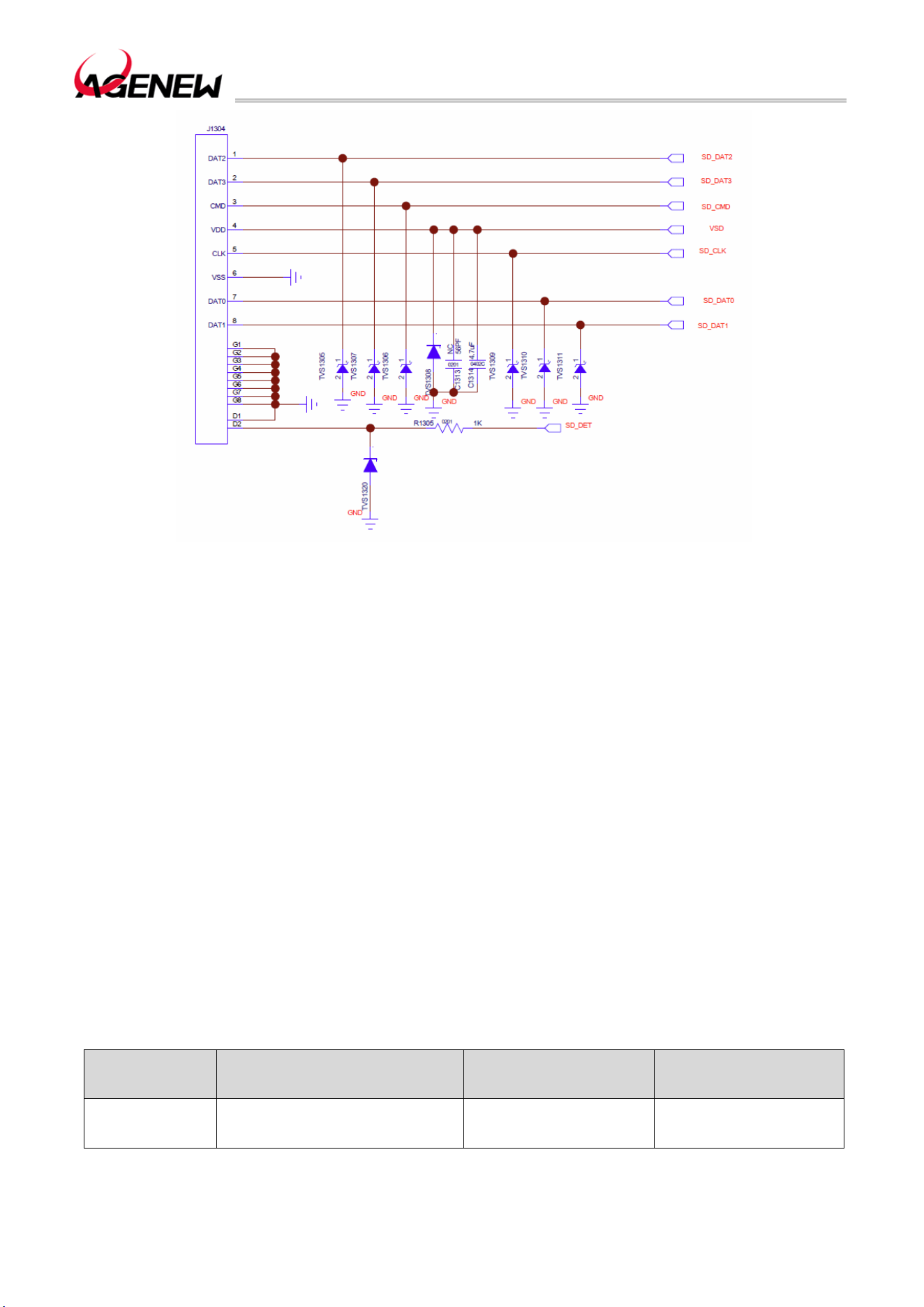
H1503BQ_Hardware Design Guide
WWW.AGENEWTECH.COM
36
Figure 13 Refer To The Circuit Diagram For The SD Card Interface
Remark:
SD_VDD is an SD card peripheral power supply capable of delivering up to approximately
800mA; Due to the large power supply current, it is recommended that the trace width is more
than 0.5mm; In order to ensure the stability of the supply current, 4.7uF and 56pF capacitors
need to be connected in parallel on the SD card deck side.
CMD, CLK, DATA0, DATA1, DATA2, and DATA3 are all high-speed signal lines, and these
signal lines should not be crossed with other traces during the PCB design process, and the
traces should be placed in the inner layer as much as possible. CLK, CMD, DATA0, DATA1,
DATA2, and DATA3 traces are recommended to be of equal length.
Layout line length requirements:
⚫ CMD/CLK needs to be grounded to reduce interference.
⚫ The total length of the cable shall not exceed 101.6mm. When the trace length is L,
50.8mm<L<101.6mm, the damping resistor needs to be reserved.
⚫ The length difference of CMD, DATA, CLK traces cannot exceed 7.62mm.
Table 12 The Length Of The SDIO Trace Inside The Module
Pin Number Signal Length (mm) Remark
39 SD_CLK 46.50173

H1503BQ_Hardware Design Guide
WWW.AGENEWTECH.COM
37
40 SD_CMD 44.62509
41 SD_DATA0 44.91917
42 SD_DATA1 44.85304
43 SD_DATA2 42.20130
44 SD_DATA3 42.09036
3.13 GPIO Interface
H1503BQ has a rich GPIO interface with an interface voltage range of 1.8V and the pins
are defined as follows:
Table 13 List of GPIO Interfaces
Pin Name
Pin
Numb
er
I/O Description DC Characteristics Remark
GPIO6 33 IO GPIO
VOLmax=0.45V
VOHmin=1.35V
Multiplex EINT6
GPIO89 90 IO GPIO
VOLmax=0.45V
VOHmin=1.35V
GPIO10 97 IO GPIO
VOLmax=0.45V
VOHmin=1.35V
Multiplex EINT10
GPIO9 98 IO GPIO
VOLmax=0.45V
VOHmin=1.35V
Multiplex EINT9
GPIO150 112 IO GPIO
VOLmax=0.45V
VOHmin=1.35V
GPIO151 113 IO GPIO
VOLmax=0.45V
VOHmin=1.35V
GPIO3 115 IO GPIO
VOLmax=0.45V
VOHmin=1.35V
Multiplex EINT3
GPIO88 123 IO GPIO
VOLmax=0.45V
VOHmin=1.35V
GPIO160 124 IO GPIO
VOLmax=0.45V
VOHmin=1.35V
GPIO87 127 IO GPIO
VOLmax=0.45V
VOHmin=1.35V
GPIO7 153 IO GPIO
VOLmax=0.45V
VOHmin=1.35V
Multiplex EINT7
GPIO8 154 IO GPIO
VOLmax=0.45V
VOHmin=1.35V
Multiplex EINT8
GPIO107 163 IO GPIO
VOLmax=0.45V
VOHmin=1.35V
H1503BQ_Hardware Design Guide
WWW.AGENEWTECH.COM
38
GPIO109 164 IO GPIO
VOLmax=0.45V
VOHmin=1.35V
GPIO108 165 IO GPIO
VOLmax=0.45V
VOHmin=1.35V
GPIO165 177 IO GPIO
VOLmax=0.45V
VOHmin=1.35V
GPIO176 178 IO GPIO
VOLmax=0.45V
VOHmin=1.35V
GPIO167 179 IO GPIO
VOLmax=0.45V
VOHmin=1.35V
GPIO166 182 PO GPIO
VOLmax=0.45V
VOHmin=1.35V
GPIO172 186 IO GPIO
VOLmax=0.45V
VOHmin=1.35V
GPIO168 201 DO GPIO
VOLmax=0.45V
VOHmin=1.35V
GPIO164 232 DO GPIO
VOLmax=0.45V
VOHmin=1.35V
GPIO169 239 DI GPIO
VOLmax=0.45V
VOHmin=1.35V
GPIO152 267 IO GPIO
VOLmax=0.45V
VOHmin=1.35V
3.14 I2C Interface
H1503BQ 7 sets of I2C interfaces are available. The interface reference voltage domain
is 1.8V. Only master mode is supported. It can support various sensors using I2C
communication, such as acceleration, gyroscope, direction, light, temperature, pressure
sensors, etc.
Table 14 I2C Interface Pin Definition
Pin Name
Pin
Number
I/O Description
Dc
Characteristics
Remark
SCL1 91 DO I2C1 serial clock
VOLmax=0.45V
VOHmin=1.35V
No external pull-up
is required
SDA1 92 IO I2C1 serial data
VOLmax=0.45V
VOHmin=1.35V
No external pull-up
is required
SCL2 166 DO I2C2 serial clock
VOLmax=0.45V
VOHmin=1.35V
No external pull-up
is required
SDA2 205 IO I2C2 serial data
VOLmax=0.45V
VOHmin=1.35V
No external pull-up
is required
SCL3 167 DO I2C3 serial clock
VOLmax=0.45V
VOHmin=1.35V
No external pull-up
is required

H1503BQ_Hardware Design Guide
WWW.AGENEWTECH.COM
39
SDA3 168 IO I2C3 serial data
VOLmax=0.45V
VOHmin=1.35V
No external pull-up
is required
SCL4 169 DO I2C4 serial clock
VOLmax=0.45V
VOHmin=1.35V
No external pull-up
is required
SDA4 170 IO I2C4 serial data
VOLmax=0.45V
VOHmin=1.35V
No external pull-up
is required
SCL5 83 DO I2C5 serial clock
VOLmax=0.45V
VOHmin=1.35V
No external pull-up
is required
SDA5 84 IO I2C5 serial data
VOLmax=0.45V
VOHmin=1.35V
No external pull-up
is required
3.15 SPI Interface
H1503BQ 5 sets of SPI interfaces are open by default, which can be used for fingerprint
recognition and other designs.
Table 15 SPI Interface Pin Definition
Pin Name
Pin
Number
I/O Description Dc Characteristics Remark
SPI0_CSB 117 DO Chip selection signal
VOLmax=0.45V
VOHmin=1.35V
SPI0_CLK 116 DO Clock signals
VOLmax=0.45V
VOHmin=1.35V
SPI0_MO 118 DO Data output
VOLmax=0.45V
VOHmin=1.35V
SPI0_MI 119 DI Data Input
VILmax=0.63V
VIHmin=1.17V
SPI1_CSB 107 DO Chip selection signal
VOLmax=0.45V
VOHmin=1.35V
Reuse I2S1_BCK
SPI1_CLK 108 DO Clock signals
VOLmax=0.45V
VOHmin=1.35V
Reuse I2S1_DO
SPI1_MO 109 DO Data output
VOLmax=0.45V
VOHmin=1.35V
Reuse I2S1_LRCK
SPI1_MI 110 DI Data Input
VILmax=0.63V
VIHmin=1.17V
Reuse I2S1_MCK
SPI2_CSB 103 DO Chip selection signal
VOLmax=0.45V
VOHmin=1.35V
SPI2_CLK 104 DO Clock signals
VOLmax=0.45V
VOHmin=1.35V
SPI2_MO 105 DO Data output
VOLmax=0.45V
VOHmin=1.35V
SPI2_MI 106 DI Data Input
VILmax=0.63V
VIHmin=1.17V
SPI3_CSB 99 DO Chip selection signal
VOLmax=0.45V
VOHmin=1.35V
Reuse I2S2_BCK
H1503BQ_Hardware Design Guide
WWW.AGENEWTECH.COM
40
SPI3_CLK 100 DO Clock signals
VOLmax=0.45V
VOHmin=1.35V
Reuse I2S2_DO
SPI3_MO 101 DO Data output
VOLmax=0.45V
VOHmin=1.35V
Reuse I2S2_LRCK
SPI3_MI 102 DI Data input
VILmax=0.63V
VIHmin=1.17V
Reuse I2S2_MCK
SPI4_CSB 242 DO Chip selection signal
VOLmax=0.45V
VOHmin=1.35V
SPI4_CLK 270 DO Clock signals
VOLmax=0.45V
VOHmin=1.35V
SPI4_MO 264 DO Data output
VOLmax=0.45V
VOHmin=1.35V
SPI4_MI 265 DI Data input
VILmax=0.63V
VIHmin=1.17V
3.16 ADC Interface
H1503BQ One ADC channel is provided with the following pin definitions:
Table 16 ADC Interface Pin Definition
ADC Interface
Pin Name
Pin
Number
I/O Description Remark
ADC_IN2 128 AI
ADC analog sampling
input
General-purpose ADC interface
The ADC pins can support up to 12 bit precision resolution.
3.17 Motor Drive Interface
H1503BQ The pins of the motor drive interface are defined as follows:
Table 17 Motor Drive Interface Pin Definition
Motor Drive Interface
Pin Name
Pin
Number
I/O Description
DC
Characteristics
Remark
VIBR_DRV 28 PO
Vibration motor power
output
Vmax=3.3V
Vmin=1.2V
Vnorm=2.8V
Imax=200mA
The motor is driven by a specialized circuit, and the reference design circuit is as follows:
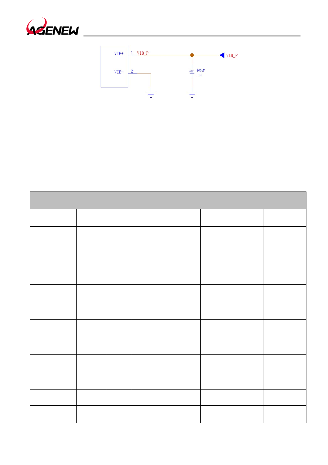
H1503BQ_Hardware Design Guide
WWW.AGENEWTECH.COM
41
Figure 14 Motor Drive Circuit
3.18 LCM Interface
H1503BQ The video output interface (LCM interface) is based on the MIPI_DSI standard,
supporting 4 groups of high-speed differential data transmission, each group up to 1.2Gbps,
and supporting HD+1280×800 resolution. The LCM interface pins are defined as follows:
Table 18 LCM Interface Pin Definition
LCM Interface
Pin Name
Pin
Number
I/O Description Dc Characteristics Remark
DISP_PWM 29 DO PWM output
VOLmax=0.45V
VOHmin=1.35V
Adjust the
brightness of
the backlight
LCD_RST 49 DO LCD reset signal
VOLmax=0.45V
VOHmin=1.35V
1.8V voltage
domain
Valid low
DSI_TE 50 DO LCD tearing effect signal
VOLmax=0.45V
VOHmin=1.35V
1.8V voltage
domain
DSI_CKP 53 AO LCD MIPI clock positive
DSI_CKN 52 AO LCD MIPI clock negative
DSI_D0P 55 AO
LCD MIPI data 0
positive
DSI_D0N 54 AO
LCD MIPI data 0
negative
DSI_D1P 57 AO
LCD MIPI data 1
positive
DSI_D1N 56 AO
LCD MIPI data 1
negative
DSI_D2P 59 AO
LCD MIPI data 2
positive
DSI_D2N 58 AO
LCD MIPI data 2
negative
H1503BQ_Hardware Design Guide
WWW.AGENEWTECH.COM
42
DSI_D3P 61 AO
LCD MIPI data 3
positive
DSI_D3N 60 AO
LCD MIPI data 3
negative
The LCM interface reference circuit is as follows:
15 LCM Circuit Reference Design
MIPI is a high-speed signal line, and it is recommended to connect the common-mode
inductor in series close to the LCM to reduce electromagnetic radiation interference.
When customers need a compatible screen design, the LCD_ID pin of the LCM should
be connected to the GPIO port of the module, but it should be noted that the output voltage
of the LCD_ID cannot exceed the voltage range of the GPIO pin.
H1503BQ The module does not have a backlight driver output, only a PWM control port
is left, and the user needs to add a backlight driver circuit on the backboard to drive the LCM
backlight.
3.19 Touchscreen Interface
H1503BQ provides 1 set of I2C interfaces by default for connecting to the touch screen
(TP), providing both the required power and interrupt pins. The touch screen interface pins of
the module are defined as follows:
Table 19 Touchscreen Interface Pin Definition
Touchscreen Interface
H1503BQ_Hardware Design Guide
WWW.AGENEWTECH.COM
43
Pin Name
Pin
Number
I/O Description
DC
Characteristics
Remark
TP_RST 31 DO
Touch screen reset
signal
VOLmax=0.45V
VOHmin=1.35V
1.8V voltage domain
Valid low
TP_INT 30 DI
The touch screen
interruption signal
VOLmax=0.45V
VOHmin=1.35V
1.8V voltage domain
SCL0 47 DO Touchscreen I2C clock
VOLmax=0.45V
VOHmin=1.35V
No external pull-up is
required
SDA0 48 IO Touchscreen I2C data
VOLmax=0.45V
VOHmin=1.35V
No external pull-up is
required
The touch screen interface reference circuit is shown in the following figure:
Figure 16 Touch Screen Interface Reference Circuit
3.20 Camera Interface
The H1503BQ video input interface is based on the MIPI CSI standard, which supports
dual-camera 4-lane camera (4-lane+4-lane) or triple camera (4-lane+2-lane+1-lane);
H1503BQ supports up to 21MP pixel camera; The camera and photo quality are determined
by a variety of factors such as camera sensor, lens specifications, and so on.
Here are a few things to keep in mind:
VDDCAMA can be reused when multiple cameras are not working at the same time. If
you are working at the same time, you can try to share VDDCAMA but reserve an external
LDO to prevent interference.

H1503BQ_Hardware Design Guide
WWW.AGENEWTECH.COM
44
If the VDDCAM power supply requirements of the camera exceed the range of 1.0~1.4V,
an external LDO is required.
If the camera module has a pixel of 16M or more, VDDCAMA needs to be backed up by
an external LDO.
RST and PWDN signals cannot be multiplexed by multiple cameras or configured for other
functions;
If you must share MCLK, make sure that the power-on and initialization timing (power and
clock) can meet the requirements of each camera.
Multiple cameras can be mounted on one I2C bus, and the I2C addresses of CMOS
sensor, VCM driver, and EEPROM on the same I2C bus cannot conflict.
EEPROM is required for dual cameras, EEPROM is required for single cameras above
13M, and EEPROM is not less than 64kbit;
The dual-camera/multi-camera module draws out the synchronization signal VSYNC,
which is used for hardware frame synchronization.
The camera interface is defined as follows:
Table 20 Camera Interface Pin Definition
Camera Interface
Pin Name
Pin
Number
I/O Description
DC
Characteristics
Remark
VCAM_AVDD 129 PO
Camera analog
power supply
Vnorm=2.8V
IOmax =200mA
To supply power to
the analog voltage
part of the camera,
1.0uF ~ 4.7uF bypass
capacitor needs to be
added when using
VCAM_AF 193 PO Output 2.8V
Vnorm=2.8V
IOmax=400mA
To power the focusing
motor of the external
camera, 1.0uF ~
2.2uF bypass
capacitors need to be
added when using
VCAMD_PMU 192 PO
Digital power supply
for the camera
Vnorm=1.2V
IOmax=400mA
To supply power to
the digital voltage part
of the camera, a
bypass capacitor of
1.0uF ~ 2.2uF needs
to be added when
using
VCAM_IOVDD 125 PO
Camera IO power
supply
Vnorm=1.8V
IOmax=300mA
To supply power to
the I/O part of the
camera, a bypass
capacitor of
1.0uF~2.2uF needs to
be added when using

H1503BQ_Hardware Design Guide
WWW.AGENEWTECH.COM
45
CSI0_CLKN 157 AO
MIPI CSI0 clock is
negative
Multiplex 2-lane
cameras
CSI0A_LN1N
CSI0_CLKP 196 AO
MIPI CSI0 clock
positive
Multiplex 2-lane
cameras
CSI0A_LN1P
CSI0_LN0N 158 AI
MIPI CSI0 data 0
negative
Multiplex 2-lane
cameras
CSI0A_CLKN
CSI0_LN0P 197 AI
MIPI CSI0 data 0
positive
Multiplex 2-lane
cameras
CSI0A_CLKP
CSI0_LN1N 159 AI
MIPI CSI0 data 1
negative
Multiplex the 1lane
camera
CSI0B_LN0N
CSI0_LN1P 198 AI
MIPI CSI0 data 1
positive
Multiplex 1-lane
cameras
CSI0B_LN0P
CSI0_LN2N 160 AI
MIPI CSI0 data 2
negative
Multiplex 2-lane
cameras
CSI0A_LN0N
CSI0_LN2P 199 AI
MIPI CSI0 data 2
positive
Multiplex 2-lane
cameras
CSI0A_LN0P
CSI0_LN3N 161 AI
MIPI CSI0 data 3
negative
Multiplex the 1lane
camera
CSI0B_CLKN
CSI0_LN3P 200 AI
MIPI CSI0 data 3
positive
Multiplex 1-lane
cameras
CSI0B_CLKP
CSI1_CLKN 63 AO
MIPI CSI0 clock
negative
CSI1_CLKP 64 AO
MIPI CSI0 clock
positive
CSI1_LN0N 65 AI
MIPI CSI0 data 0
negative
CSI1_LN0P 66 AI
MIPI CSI0 data 0
positive
CSI1_LN1N 67 AI
MIPI CSI0 data 1
negative
CSI1_LN1P 68 AI
MIPI CSI0 data 1
positive
CSI1_LN2N 72 AI
MIPI CSI0 data 2
negative
CSI1_LN2P 73 AI
MIPI CSI0 data 2
positive
CSI1_LN3N 70 AI
MIPI CSI0 data 3
negative
CSI1_LN3P 71 AI
MIPI CSI0 data 3
positive

H1503BQ_Hardware Design Guide
WWW.AGENEWTECH.COM
46
CAM0_MCLK 74 DO
Camera 0 clock
signal
VOLmax=0.45V
VOHmin=1.35V
1.8V voltage domain
CAM1_MCLK 75 DO
Camera 1 clock
signal
VOLmax=0.45V
VOHmin=1.35V
1.8V voltage domain
CAM0_RST 79 DO
Camera 0 reset
signal
VOLmax=0.45V
VOHmin=1.35V
CAM0_PDN 80 DO
Camera 1 shutdown
signal
VOLmax=0.45V
VOHmin=1.35V
CAM1_RST 81 DO
Camera 0 reset
signal
VOLmax=0.45V
VOHmin=1.35V
CAM1_PDN 82 DO
Camera 1 shutdown
signal
VOLmax=0.45V
VOHmin=1.35V
SCL2 166 DO
Camera I2C clock
signal
VOLmax=0.45V
VOHmin=1.35V
No external pull-up is
required
SDA2 205 IO
Camera I2C data
signal
VOLmax=0.45V
VOHmin=1.35V
No external pull-up is
required
The 2-way camera reference circuit is as follows:
H1503BQ_Hardware Design Guide
WWW.AGENEWTECH.COM
47
Figure 17 2-Way Camera Reference Design
The 3-way camera reference circuit is as follows:
H1503BQ_Hardware Design Guide
WWW.AGENEWTECH.COM
48
Figure 18 3-way Camera reference design
Remark
MIPI is a high-speed signal line, and customers can connect industrial mode inductors in
series on MIPI signal lines according to project requirements to improve electromagnetic
radiation interference.
H1503BQ_Hardware Design Guide
WWW.AGENEWTECH.COM
49
3.20.1 Design Considerations
⚫ When designing your schematic, pay attention to the correct video device interface
definition. Different video components have different definitions of connectors, and you need
to pay attention to the correct connection between connectors and components.
⚫MIPI is a high-speed signal line with a transmission rate of up to 2.5Gbps; 100Ω
differential impedance for wiring; It is recommended that the wiring be placed on the inner
layer and not cross with other signal lines. For MIPI traces of the same video component,
equal length control is required. It is recommended to maintain 1.5 times the line width spacing
between MIPI signal lines to prevent crosstalk; When doing 100Ω differential impedance
matching, do not cross-connect different GND planes to ensure the consistency of impedance.
⚫ MIPI wiring requirements are as follows:
a) The total length of the cable shall not exceed 76.2mm;
b) The differential impedance of the control is required to be 100Ω and the error is ±15%.
Table 21 The Length of The MIPI Trace Inside The Module
Pin
Number
Signal Length (mm). Length Difference (P-N)
157 CSI0_CLKN 20.71366
0.14466
196 CSI0_CLKP 20.56900
158 CSI0_LN0N 20.9705
-0.33215
197 CSI0_LN0P 20.63835
159 CSI0_LN1N 20.53910
-0.04024
198 CSI0_LN1P 20.49866
160 CSI0_LN2N 20.36316
-0.09911
199 CSI0_LN2P 20.26404
161 CSI0_LN3N 20.33060
0.17818
200 CSI0_LN3P 20.50878
63 CSI1_CLKN 25.84925
-0.43205
64 CSI1_CLKP 25.41720
H1503BQ_Hardware Design Guide
WWW.AGENEWTECH.COM
50
65 CSI1_LN0N 25.27341
0.05422
66 CSI1_LN0P 25.32763
67 CSI1_LN1N 25.38328
-0.26716
68 CSI1_LN1P 25.11612
72 CSI1_LN2N 25.45761
-0.41528
73 CSI1_LN2P 25.04233
70 CSI1_LN3N 25.07939
0.41109
71 CSI1_LN3P 25.49058
3.20.2 Flashlight Interface
H1503BQ There is only one Flashlight interface, and the pins of this interface are defined
as follows:
Table 22 Flashlight Interface Pin Definition
Flashlight Interface
Pin Name
Pin
Number
I/O Description
DC
Characteristics
Remark
FLASH_LE
D
180 AO Flash positive output Iomax=1A
3.21 Sensor Interface
H1503BQ Connect to sensors via I2C communication, support ALS/PS, Compass, G-sensor,
Gyroscope and other sensors.
Table 23 Sensor Interface Pin Definition
Sensor Interface
Pin Name
Pin
Number
I/O Description
DC
Characteristics
Remark
SCL1 91 DO I2C1 serial clock
VOLmax=0.45V
VOHmin=1.35V
No external pull-up is
required
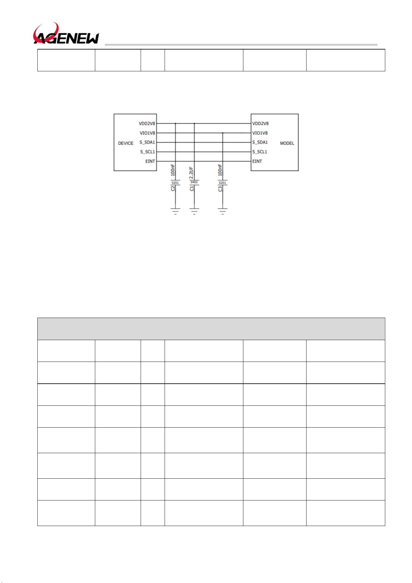
H1503BQ_Hardware Design Guide
WWW.AGENEWTECH.COM
51
SDA1 92 IO I2C1 serial data
VOLmax=0.45V
VOHmin=1.35V
No external pull-up is
required
The sensor reference circuit is as follows:
Figure 19 Sensor Reference Design Circuit
3.22 Audio Interface
H1503BQ provides three analog audio input channels and four analog audio output
channels. The pins of the audio interface are defined in the following table:
Table 24 Audio interface pin definition
Audio Interface
Pin Name
Pin
Number
I/O Description
DC
Characteristics
Remark
MICBIAS0 147 PO
MIC0、MIC2 bias
voltage
VO=0V~2.94V
MIC0_P 4 TO
Main microphone
input positive
MIC0_N 5 TO
Main microphone
input negative
MIC2_P 148 TO
Secondary
microphone input
positive
MIC2_N 149 TO
Secondary
microphone input
negative
EAR_P 8 TO
Differential handset
output positive
EAR_N 9 TO
Differential earpiece
outputs a negative
pole

H1503BQ_Hardware Design Guide
WWW.AGENEWTECH.COM
52
LINEOUT_P 10 TO
Differential line out
output positive
LINEOUT_N 11 TO
Differential line out
output negative
MICBIAS1 155 PO
Headphone MIC bias
voltage
VO=0V~2.94V
HP_MIC 6 TO Headphone MIC input
AU_HPR 136 TO
Headphone right
channel
AU_REFN 137 TO
Headphone reference
ground
If not, it needs to be
grounded
AU_HPL 138 TO
Headphone left
channel
⚫ Modules have: 3 Group audio inputs, including: 2 Group Differential Input Channels
and 1 group of single-ended input channels;
⚫ The receiver interface adopts differential output;
⚫ The lineout interface uses differential output; if an external speaker is required, an
audio amplifier must be added outside the module.
⚫ The headphone jack is a stereo left and right channel output, and the headset has a
plug-in detection function.
3.22.1 Microphone Interface Reference Circuit
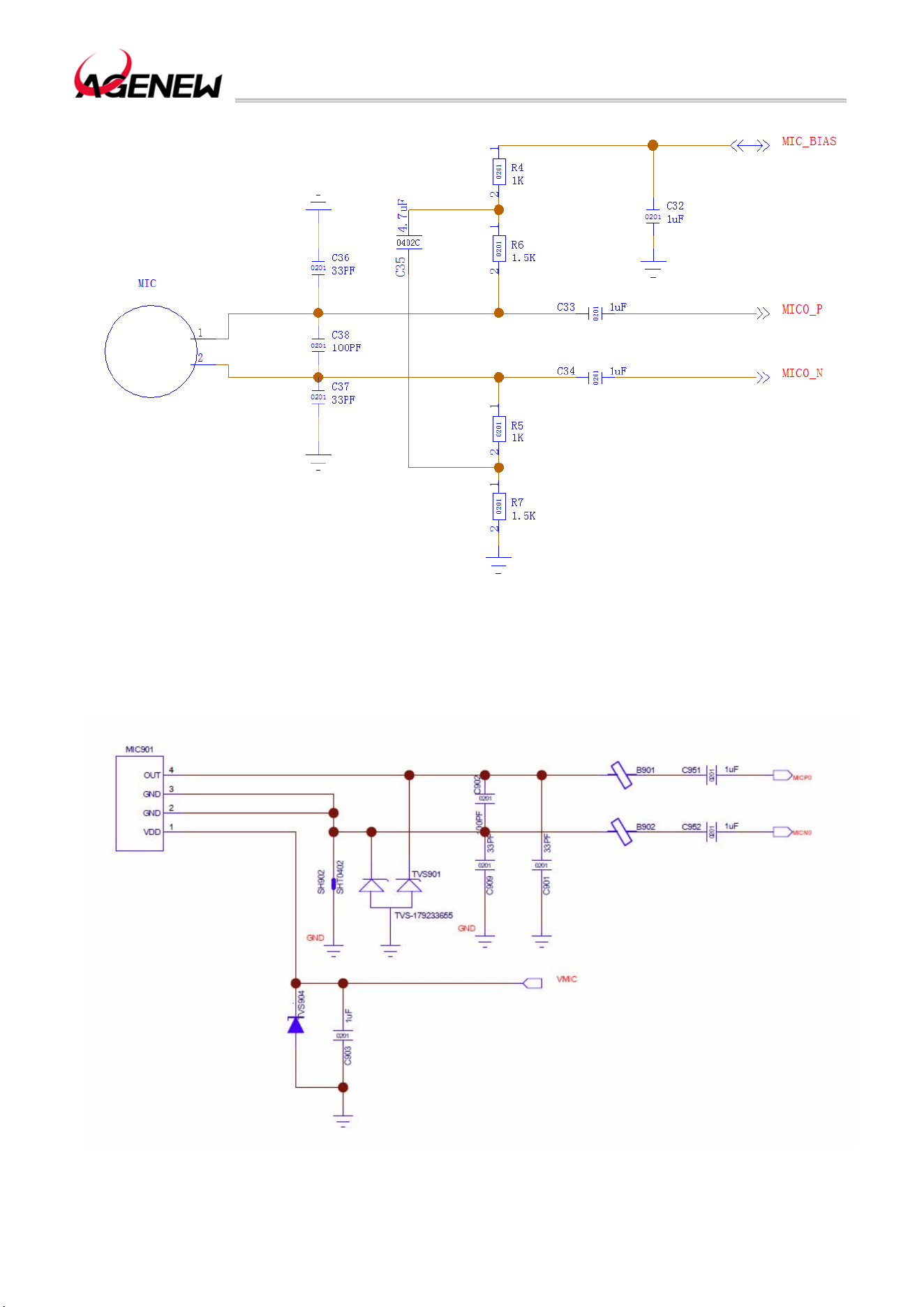
H1503BQ_Hardware Design Guide
WWW.AGENEWTECH.COM
53
Figure 20 Standing Microphone Reference Circuit (The Sub-MIC Wiring Method Is The Same As The
Main MIC)
Figure 21 Silicon Microphone Reference Circuit (The Wiring Method Of The Sub-MIC Is The Same As
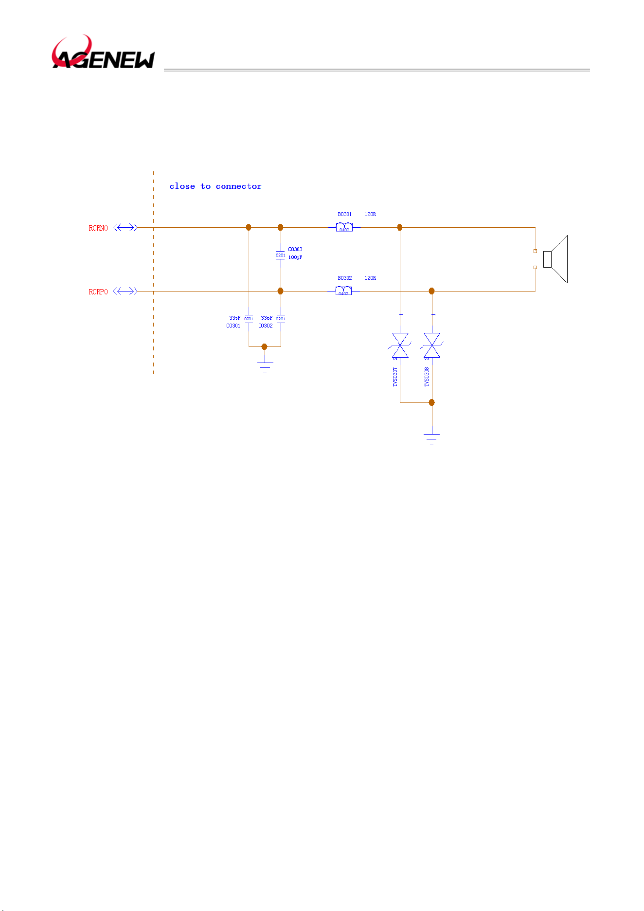
H1503BQ_Hardware Design Guide
WWW.AGENEWTECH.COM
54
That Of The Main MIC)
3.22.2 Handset Interface Reference Circuit
Figure 22 Handset Output Interface Reference Circuit
3.22.3 Headphone Interface Reference Circuit
If use the 3.5mm headphone interface, the reference design is as follows:
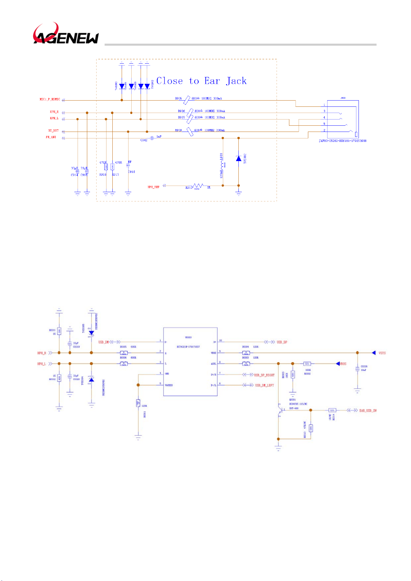
H1503BQ_Hardware Design Guide
WWW.AGENEWTECH.COM
55
Figure 23 Headphone Jack Reference Circuit
You can also use the TYPEC port to support analog headphones and digital headphones,
you only need to connect a USB2.0 and Audio Swith IC and EU/US headphone switcher IC,
take the BCT4321N of the BROADCHIP brand and the WAS4766C of the WILLSEMI brand
as examples, the reference circuit is as follows:
Figure 24 USB2.0 and Audio Swith IC Reference Circuit
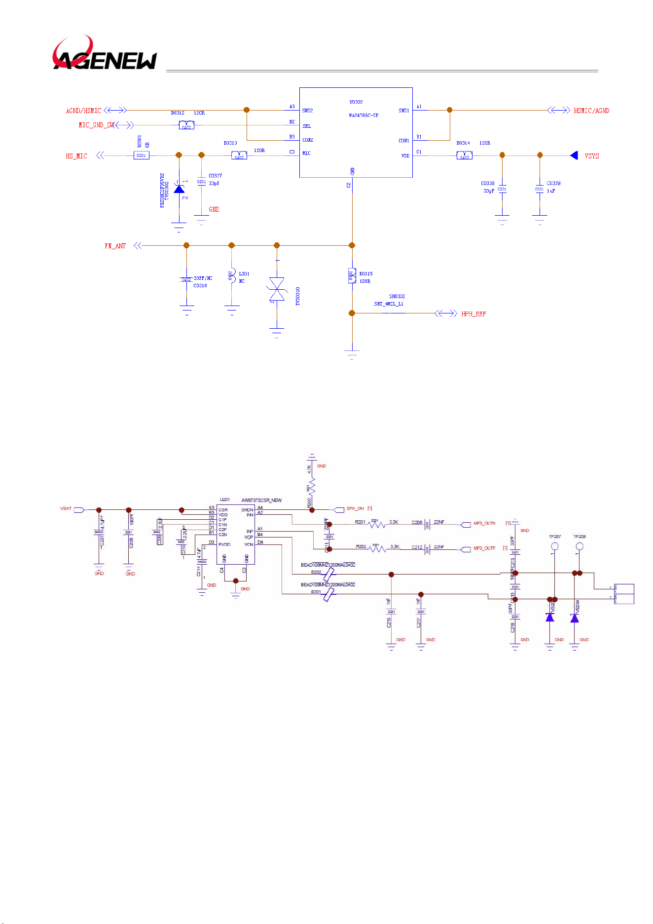
H1503BQ_Hardware Design Guide
WWW.AGENEWTECH.COM
56
Figure 25 EU/US headphone switcher IC Reference Circuit
3.22.4 Speaker Interface Reference Circuit
Figure 26 Speaker Interface Reference Circuit
H1503BQ need to use an external audio amplifier to drive the speakers.
3.22.5 Audio Signal Design Considerations
Handheld microphones and hands-free microphones are recommended to use electret
microphones with built-in RF filtering dual condensers (e.g., 10pF and 33pF); Filtering out RF

H1503BQ_Hardware Design Guide
WWW.AGENEWTECH.COM
57
interference from the source of the interference minimizes coupled TDD noise. The 33pF
capacitor is used to filter out high-frequency interference when the module is operating at
EGSM900. If you don't add this capacitor, you may hear TDD noise during calls. At the same
time, the 10pF capacitance is used to filter out high-frequency interference when operating at
DCS1800. It should be noted that since the resonance point of a capacitor depends largely
on the material and manufacturing process of the capacitor, it is necessary to consult the
supplier of the capacitor when selecting a capacitor to select the most appropriate capacitance
value to filter out the high-frequency noise during operation.
The severity of high-frequency interference during GSM transmission is usually primarily
dependent on the customer's application design. In some cases, the TDD of EGSM900
The noise is severe, and in some cases, the TDD noise of the DCS1800 is severe.
Therefore, customers can choose the required filter capacitor according to the test results,
and sometimes even do not need to paste this kind of filter capacitor.
The antenna should be positioned as far away from the audio element and audio traces
as possible to reduce radiated interference; The power and audio traces should not be parallel
and should be as far away from the audio traces as possible.
Differential audio traces must follow the Layout rules for the differential signal .
3.23 Forced Download Interface
Table 25 Forced Download Pin Definitions
Forced Interface
Pin Name
Pin
Number
I/O Description DC Characteristics Remark
THEFT- 96 OF
Volume reduction
and forced
downloads
VOLmax=0.45V
VOHmin=1.35V
KCOL0 is an emergency download interface. When the power is off, pull the KCOL0 pin
to the ground, and the module can enter the forced download mode, which is used for the
final processing when the product cannot be started normally due to a fault, and the interface
can be reused as a volume key. In order to facilitate the subsequent software upgrade and
debugging of the product, please reserve this reference circuit.
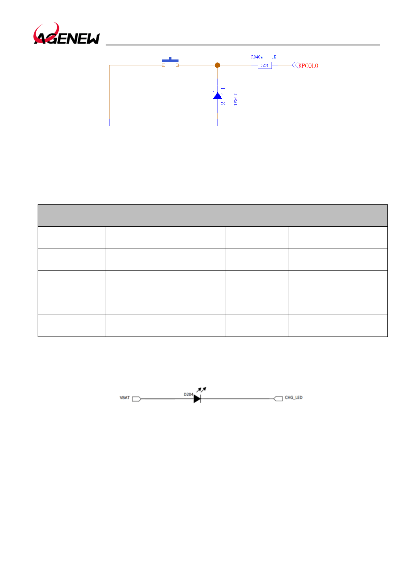
H1503BQ_Hardware Design Guide
WWW.AGENEWTECH.COM
58
Figure 27 Forced Download Interface Reference Circuit
3.24 LEDs Indicator Interface
Table 26 LEDs Indicator Interface Pin Definitions
LEDs Indicate The Interface
Pin Name
Pin
Number
I/O Description
DC
Characteristics
Remark
CHG_LED 195 AI
Charging
indication
Input Current Range:
1mA~6mA
LED_R 252 AI
LED control
negative
The detached version is
GPIO174
LED_G 253 AI
LED control
negative
The detached version is
GPIO173
LED_B 249 AI
LED control
negative
The detached version is
GPIO175
The LED indicator interface reference circuit as follows:
Figure 28 LEDs indicator interface reference circuit
When GPIO control is used, an external drive circuit is required.

H1503BQ_Hardware Design Guide
WWW.AGENEWTECH.COM
59
4 Wi-Fi and BT
The H1503BQ module provides a Wi-Fi, BT, GNSS common antenna interface
ANT_WI-FI/BT/GNSS with an impedance control of 50Ω. Customers can connect
external PCB antennas, suction cup antennas or ceramic antennas through this
interface to achieve Wi-Fi, BT and GNSS functions.
4.1 Wi-Fi Overview
The H1503BQ module supports 2.4GHz and 5GHz WLAN wireless communication, and
supports 802.11a, 802.11b, 802.11g, 802.11n and ac standards, with a maximum speed of
433Mbps. Its characteristics are as follows:
⚫ Support WIFI and BT FDD operation modes
⚫ Supports global WIFI 5G channels, including the latest frequency band (5925MHz)
⚫ Support transmit power control for each WIFI packet
⚫ PVT self-calibration is supported to cope with environmental changes
⚫ Supports a wide range of crystal oscillator clock frequencies
⚫HT20 and HT40 support MCS 0-7
⚫VHT20 support MCS 0-8
⚫VHT40 and VHT80B support MCS 0-9
4.1.1 Wi-Fi Performance Metrics
The following table lists the transmit and receive performance of H1503BQ Wi-Fi function.
Table 27 Wi-Fi Transmit Performance
Standard Speed Output Power
2.4GHz
802.11b 1Mbps 16dBm±2.5dB
802.11b 11Mbps 16dBm±2.5dB
802.11g 6Mbps 16dBm±2.5dB
802.11g 54Mbps 14dBm±2.5dB
H1503BQ_Hardware Design Guide
WWW.AGENEWTECH.COM
60
802.11n HT20 MCS0 15dBm±2.5dB
802.11n HT20 MCS7 13Bm±2.5dB
802.11nHT40 MCS0 14Bm±2.5dB
802.11nHT40 MCS7 13dBm±2.5dB
5GHz
802.11a 6Mbps 15dBm±2.5dB
802.11a 54Mbps 13dBm±2.5dB
802.11n HT20 MCS0 15dBm±2.5dB
802.11n HT20 MCS7 13dBm±2.5dB
802.11n HT40 MCS0 15dBm±2.5dB
802.11n HT40 MCS7 13dBm±2.5dB
802.11ac VHT20 MCS0 14dBm±2.5dB
802.11ac VHT20 MCS8 13dBm±2.5dB
802.11ac VHT40 MCS0 13dBm±2.5dB
802.11ac VHT40 MCS9 12dBm±2.5dB
802.11ac VHT80 MCS0 13dBm±2.5dB
802.11ac VHT80 MCS9 12dBm±2.5dB
Table 28 WiFi Reception Performance
Standard Speed Sensitivity
2.4GHz
802.11b 1Mbps -96dBm
802.11b 11Mbps -87dBm
802.11g 6Mbps -91dBm

H1503BQ_Hardware Design Guide
WWW.AGENEWTECH.COM
61
802.11g 54Mbps -73dBm
802.11n HT20 MCS0 -90dBm
802.11n HT20 MCS7 -72dBm
802.11nHT40 MCS0 -87dBm
802.11nHT40 MCS7 -68dBm
5GHz
802.11a 6Mbps -90dBm
802.11a 54Mbps -70dBm
802.11n HT20 MCS0 -88dBm
802.11n HT20 MCS7 -69dBm
802.11n HT40 MCS0 -86dBm
802.11n HT40 MCS7 -66dBm
802.11ac VHT20 MCS8 -68dBm
802.11ac VHT40 MCS9 -64dBm
802.11ac VHT80 MCS9 -60dBm
The reference specifications are as follows:
⚫ IEEE 802.11n WLAN MAC and PHY, Oct., 2009 + IEEE 802.11-2007 WLAN MAC and
PHY, June, 2007.
⚫IEEE Std 802.11b, IEEE Std 802.11d, IEEE Std 802.11e, IEEE Std 802.11g, IEEE Std
802.11i: IEEE 802.11-2007 WLAN MAC and PHY, June, 2007.
4.2 BT Overview
H1503BQ module supports BT5.0 specification, and the modulation mode supports
GFSK, DQPSK, 8-DPSK and BLE.
⚫Max 7 BT links and 16 BLE links.
⚫Supports up to 3.5 PICONET picones at the same time.
⚫ Supports 1 SCO or eSCO (Extended Synchronous Connection Oriented) connection.
H1503BQ_Hardware Design Guide
WWW.AGENEWTECH.COM
62
The BR/EDR channel bandwidth is 1MHz and can accommodate 79 channels; The BLE
channel has a bandwidth of 2MHz and can accommodate 40 channels.
Table 29 BT Rate And Version Information
Version Data Rate
Maximum Application
Throughput Remark
Version
1.2 1Mbit/s > 80Kbit/s
2.0+EDR 3Mbit/s > 80Kbit/s
3.0+HS 24Mbit/s Please refer to 3.0+HS
4.0 24Mbit/s Please refer to 4.0 LE
4.0 48Mbit/s Please refer to 5.0 LE
The reference specifications are as follows:
⚫ Bluetooth RF TSS and TP Specification 1.2/2.0/2.0 + EDR/2.1/2.1+ EDR/3.0/3.0 + HS,
Aug. 6, 2009
⚫ Bluetooth Low Energy RF PHY Test Specification, RF-PHY. TS/4.0.0, Dec. 15, 2009
4.2.1 BT Performance Metrics
Table 30 BT Transmit and Receive Performance Metrics
Transmitter Performance
Grouping Type DH5 2-DH5 3-DH5
Transmit Power 10dBm±2.5dB 8dBm±2.5dB 8dBm±2.5dB
Receiver Performance
Grouping Type DH5 2-DH5 3-DH5
Receive
Sensitivity
-93dBm -92dBm -86dBm
H1503BQ_Hardware Design Guide
WWW.AGENEWTECH.COM
63
5 GNSS
H1503BQ smart module supports GPS, Glonass, Beidou and Galieo positioning systems.
By default, Wi-Fi, BT, and GNSS share antenna interface ANT_WI-FI/BT/GNSS. An
independent GNSS antenna interface can also be selected, and LNA needs to be designed
on the bottom board, which can effectively improve the positioning sensitivity of GNSS.
5.1 GNSS Performance Metrics
The following table lists the GNSS performance metrics for the H1503BQ module in
conducted mode.
Table 31 GNSS Performance
Parameter
Status
Reason
Typical Unit
Sensitivity (GNSS)
cold boot -146 dBm
recapture -158 dBm
trace -160 dBm
TTFF (GNSS)
cold boot 32 s
warm start 30 s
warm boot 2 s
Static Drift (GNSS) CEP-50 6 m
5.2 GNSS RF Design Guidance
If the antenna and layout are not well designed, the GNSS reception sensitivity will be
reduced, resulting in long GNSS positioning time or low positioning accuracy. The following
design principles are adhered to in GNSS RF design:

H1503BQ_Hardware Design Guide
WWW.AGENEWTECH.COM
64
⚫ GNSS and GPRS RF section (included Layout routing and antenna layout) as far
away from the design as possible to prevent the two parts from interfering with each other;
⚫ In the user system,The location layout of GNSS RF signals and RF-related
components should be far away from high-speed circuits, power supplies, large inductors, and
single-chip microcomputer clock circuits;
⚫ For designs with harsh electromagnetic environments or high requirements for
electrostatic protection, ESD protection diodes need to be added at the antenna interface; It
is necessary to choose one with ultra-low junction capacitanceESD protection diodes. It is
recommended that the junction capacitance should not exceed 0.5pF, otherwise it will affect
the impedance characteristics of the RF loop or bypass the attenuation of the RF signal;
⚫ Whether it is a feeder or a PCB trace, 50Ω impedance control is required, and the trace
should not be too long;
⚫ Please refer to Section 6.3 for GNSS antenna reference circuit design.
H1503BQ_Hardware Design Guide
WWW.AGENEWTECH.COM
65
6 Antenna Interface
H1503BQ provides 4 antenna interfaces: primary, diversity, GNSS and Wi-Fi/BT/GNSS
antennas. The characteristic impedance of each antenna port is 50Ω.
6.1 Main/Diversity Interface
The pins of the primary/diversity interface are defined in the following table:
Table 32 Main/Diversity Antenna Interface Pin Definition
Pin Name Pin Number I/O Description Remark
ANT_MAIN 87 IO Main antenna interface
50Ω characteristic
impedance
ANT_DRX 131 AI
Diversity antenna
interface
50Ω characteristic
impedance
The operating frequency bands of the module are as follows:
Table 33 H1503BQ Supported Frequency Bands
Band Downlink Uplink Unit
GSM850 869~894 824~849 MHz
EGSM900 925~960 880~915 MHz
DCS1800 1805~1880 1710~1785 MHz
PCS1900 1930~1990 1850~1910 MHz
WCDMA B2 1930~1990 1850~1910 MHz
WCDMA B4 2110~2155 1710~1755 MHz
WCDMA B5 869~894 824~849 MHz

H1503BQ_Hardware Design Guide
WWW.AGENEWTECH.COM
66
LTE-FDD B2 1930~1990 1850~1910 MHz
LTE-FDD B4 2110~2155 1710~1755 MHz
LTE-FDD B5 869~894 824~849 MHz
LTE-FDD B7 2620~2690 2500~2570 MHz
LTE-FDD B12 729~746 699~716 MHz
LTE-FDD B13 746~756 777~787 MHz
LTE-TDD B17 734~746 704~716 MHz
LTE-TDD B25 1930~1995 1850~1915 MHz
LTE-TDD B26 859~894 814~849 MHz
LTE-TDD B66 2110-2180 1710~1780 MHz
LTE-TDD B71 617~6526 663~698 MHz
TD-LTE B41 2496~2690 2496~2690 MHz
6.1.1 RF reference circuits
For the peripheral circuit design of the main antenna/diversity antenna interface, in order
to better adjust the RF performance, it is recommended to reserve a π matching circuit. The
antenna connection reference circuit is shown in the figure below. Among them, the π
matching elements (R1/C1/C2, R2/C3/C4) should be placed as close to the antenna as
possible; The capacitor is not connected by default, only the 0Ω resistor.
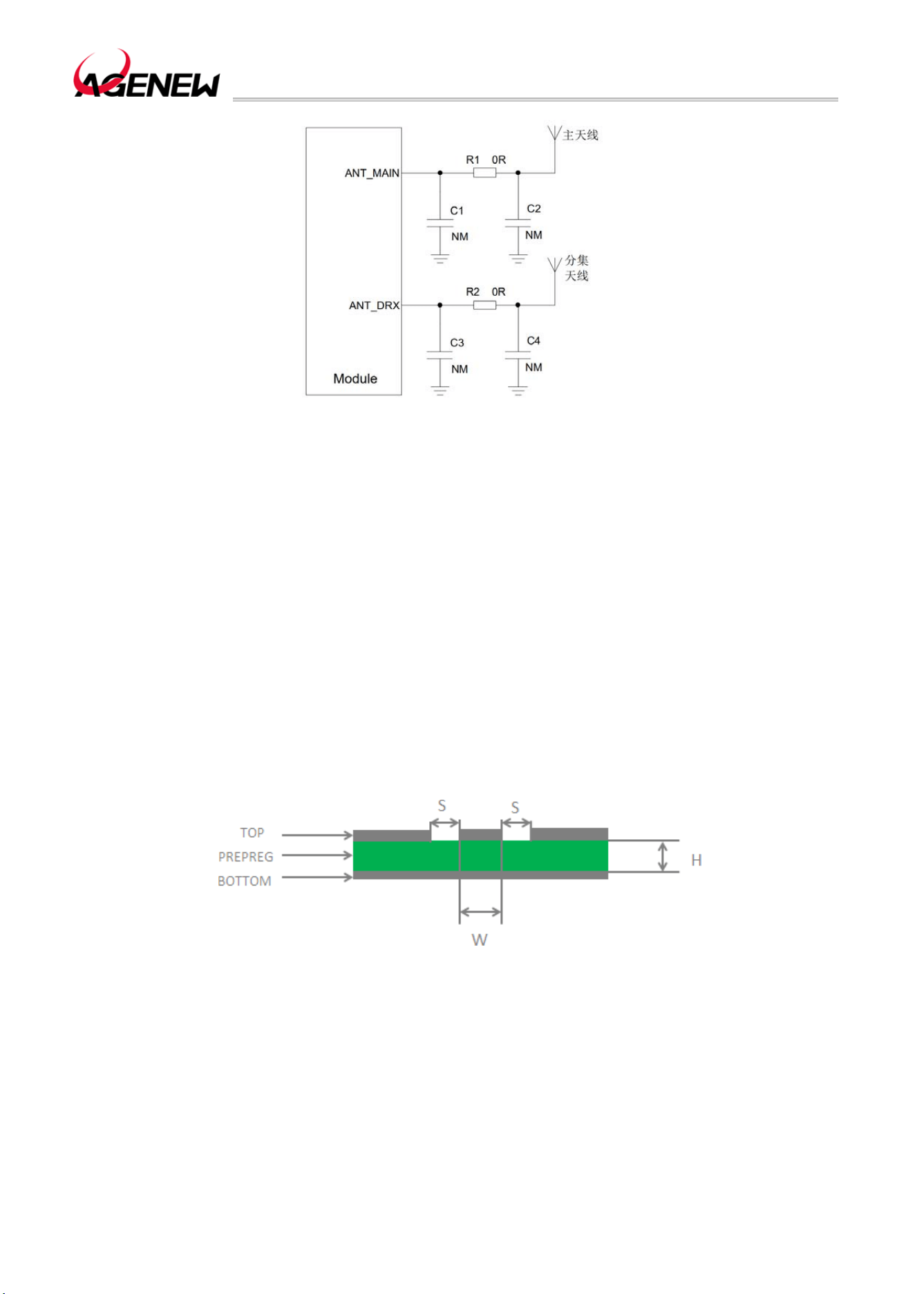
H1503BQ_Hardware Design Guide
WWW.AGENEWTECH.COM
67
Figure 29 RF reference circuits
6.1.2 RF Signal Cable Layout Reference Guide
For the user's PCB, the characteristic impedance of all RF signal lines should be
controlled at 50Ω. In general, the impedance of an RF signal line is determined by the
dielectric constant of the material, the width of the trace (W), the clearance to ground (S), and
the height of the reference ground plane (H). The characteristic impedance of the PCB is
usually controlled in two ways: microstrip line and coplanar waveguide. To illustrate the design
principles, the following diagrams illustrate the structural design of a microstrip line and a
coplanar waveguide with an impedance line controlled at 50 Ω.
⚫ Microstrip line complete structure
Figure 30 Two-layer PCB Microstrip Line Structure
⚫ Coplanar waveguide complete structure
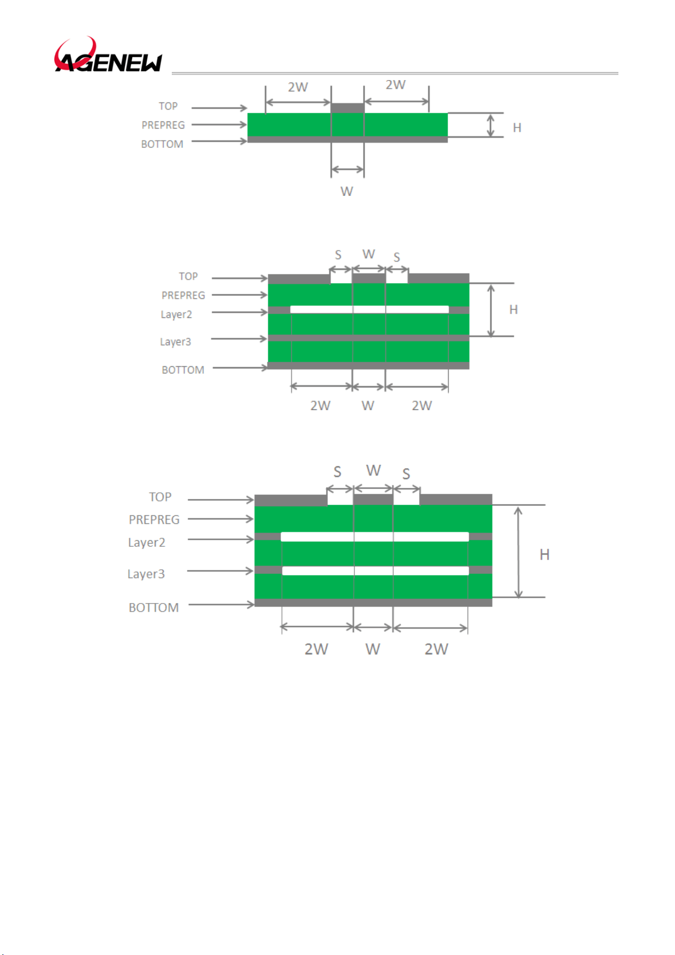
H1503BQ_Hardware Design Guide
WWW.AGENEWTECH.COM
68
Figure 31 Two-layer PCB Board Coplanar Waveguide Structure
Figure 32 Four-layer PCB Coplanar Waveguide Structure (Reference Ground Is The Third Layer)
Figure 33 Four-layer PCB Coplanar Waveguide Structure (Reference Ground Is The Fourth Layer)
In the circuit design of RF antenna interface, in order to ensure the good performance
and reliability of RF signals, the following design principles are recommended in the circuit
design:
⚫ Impedance simulation calculation tools should be used to accurately control the 50Ω
impedance of the RF signal line;
⚫ The GND pin adjacent to the RF pin should not be used as a heat dissipation pad and
should be in full contact with ground;
H1503BQ_Hardware Design Guide
WWW.AGENEWTECH.COM
69
⚫ The distance between the RF pins and the RF connector should be as short as possible;
At the same time, right-angle wiring is avoided. The recommended wiring angle is 135 degrees;
⚫ Pay attention to the establishment of the connecting device package, and keep a
certain distance between the signal pins and the ground;
⚫ The ground plane referenced by the RF signal line should be complete; Adding a
certain number of ground holes around the signal line and reference ground can help improve
RF performance; The distance between the ground hole and the signal line should be at least
twice the line width (2*W).
6.2 Wi-Fi/BT/GNSS Antenna Interface
The following table describes the Wi-Fi/BT/GNSS antenna interface pin definitions and
operating frequency bands.
Table 34 Wi-Fi/BT/GNSS Antenna Interface Pin Definition
Pin Name
Pin
Number
I/O Description Remark
ANT_WI-FI/BT/GNSS 77 IO
Wi-Fi 2.4G/Wi-Fi
5G/BT/GNSS antenna
interface
Table 35 Wi-Fi/BT Operating Frequency Bands
Type Band Unit
802.11 a/b/g/n/ac
2402~2482
5180~5825
MHz
BT5.0 2402~2480 MHz
The Wi-Fi/BT antenna connection reference circuit is shown in the figure below. Among
them, the capacitor is not pasted by default, only the 0Ω resistor.
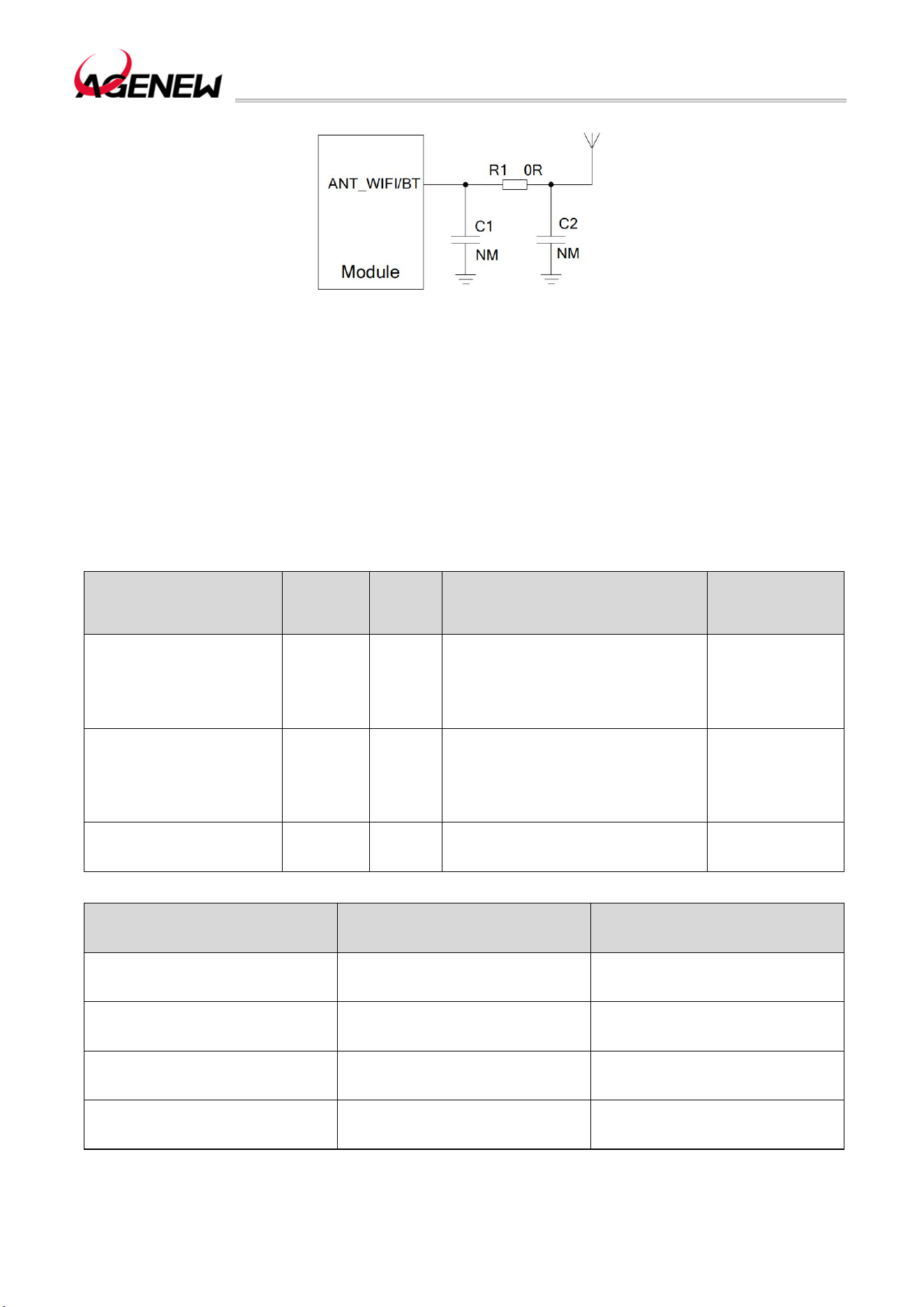
H1503BQ_Hardware Design Guide
WWW.AGENEWTECH.COM
70
34 Wi-Fi/BT Antenna Interface Reference Circuit
6.3 GNSS Antenna Interface
The following table describes the GNSS antenna interface pin definitions and operating
frequency bands.
Table 36 GNSS Antenna Interface Pin Definition
Pin Name
Pin
Number
I/O Description Remark
ANT_WI-FI/BT/GNSS 77 IO
Wi-Fi 2.4G/Wi-Fi
5G/BT/GNSS 天线接口
50Ω
characteristic
impedance
ANT_GNSS 121 AI GNSS antenna interface
50Ω
characteristic
impedance
GPIO_GPS_LNA_EN 194 DO GPS LNA enables control GPIO91
Table 37 GNSS Operating Frequency Bands
Type Band Unit
GPS 1575.42±1.023 MHz
GLONASS 1597.5~1605.8 MHz
BDS 1561.098±2.046 MHz
Galieo 1575.42±1.023 MHz
H1503BQ_Hardware Design Guide
WWW.AGENEWTECH.COM
71
6.3.1 Passive Antenna Reference Design
Passive ceramic antennas or other forms of GNSS passive antennas can be used, as
shown in the following figure:
Figure 35 Passive Antenna Reference Circuit
Remark
When the GNSS passive antenna is far away from the module (i.e., when the cable is
long) and the external loss is >2dB, in order to ensure the GNSS reception performance, it
is recommended that the module add external SAW and LNA circuits, and the LNA should be
placed close to the antenna.
6.3.2 Active antenna reference design
The power supply of the active antenna is fed from the signal line of the antenna through
the inductance of 56nH, and the common active antenna is 3.3V~5.0V. The power
consumption of the active antenna itself is very small, but the power supply is stable and clean,
so it is recommended to use a high-performance LDO to power the antenna. The active
antenna reference circuit is shown in the figure below
H1503BQ_Hardware Design Guide
WWW.AGENEWTECH.COM
72
Figure 36 Active Antenna Reference Circuit
6.4 Antenna Installation
6.4.1 Antenna Installation Requirements
The following table lists the requirements for primary, diversity, Wi-Fi/BT and GNSS
antennas:
Table 38 Antenna Requirements
Antenna Type Request
GSM/WCDMA/LTE
VSWR: ≤ 2
Gain (dBi): 1
Maximum input power (W): 50
Input Impedance (Ω): 50
Polarization Type: Vertical
Insertion Loss: < 1dB
(GSM850, EGSM900, WCDMA B5,
LTEB5/B12/B13/B17/B26/B28A/B28B/B71)
Insertion Loss: < 1.5dB
(GSM1800, PCS1900, WCDMA B2/B4 , LTE B2/B4/B25/B66)
Insertion Loss: < 2dB (LTE-FDD B7, LTE-TDD B41)
Wi-Fi/BT
VSWR: ≤ 2
Gain (dBi): 1
Maximum input power (W): 50
Input Impedance (Ω): 50
Polarization Type: Vertical
Insertion Loss: < 1dB
GNSS
Frequency range: 1559MHz~1609MHz
Polarization type: right-handed circular polarization or linear
polarization
VSWR: < 2 (typical)
Passive Antenna Gain: > 0dBi
Active Antenna Noise Figure: < 1.5dB (typical)
Active Antenna Gain: > -2dBi
H1503BQ_Hardware Design Guide
WWW.AGENEWTECH.COM
73
Active antenna built-in LNA gain: < 17dB (typical)
Total Active Antenna Gain: < 17dBi (typical)
Remark
When supporting LTE B13/B14 bands, it is not recommended to use an active GNSS
antenna and no LNA is added, but a passive GNSS antenna is recommended.
6.4.2 The Recommended RF Connector For Antenna Mounting
If using an RF connector for antenna connection, Hirose's U.FL-R-SMT connector is
recommended.
Figure 37 U.FL-R-SMT Connector Dimensions (mm)
H1503BQ_Hardware Design Guide
WWW.AGENEWTECH.COM
74
You may choose to use the U.FL-LP series cables in conjunction with the U.FL-R-SMT.
Figure 38 U.FL-LP Connection Cable Series
The following diagram shows the installation dimensions of the cable and connector:
Figure 39 Installation Dimensions (mm)
H1503BQ_Hardware Design Guide
WWW.AGENEWTECH.COM
75
7 Electrical, Reliability & RF Performance
7.1 Limit Parameters
The following table lists the maximum withstand values for voltage/current at some pins
of the module:
Table 39 Limit Parameters
Parameter Min Max Unit
VBAT -0.5 5.5 V
USB_VBUS 0 15.5 V
VBAT max current 0 4 A
Digital pin voltage -0.3 2.3 V
7.2 Power rating
Table 40 Module Power Rating
Parameter Description Condition Min Typical Max Unit
VBAT
Battery supply
voltage
The voltage must be within that
range, including voltage dips,
ripple, and spikes
3.5 3.8 4.4 V
7.3 Operating and storage temperature
The following table lists the operating and storage temperature ranges of the modules:
Table 41 Operating and Storage Temperature
Parameter Min Typical Max Unit
Normal operating
temperature
-20 +25 +80 ºC

H1503BQ_Hardware Design Guide
WWW.AGENEWTECH.COM
76
Storage
temperature range
-40 +90 ºC
7.4 Operating current
The working currents of the H1503BQ module in various working modes are shown in
the following table:
Table 42 H1503BQ Operating Current
Parameter Description Condition Min Typical Max Unit
IVBAT
Shutdown
current
Shutdown 100 uA
GSM/GPR mode
Supply current
Sleep mode (not connected to
USB)
@DRX=2
77 mA
Sleep mode (not connected to
USB)
@DRX=5
77 mA
Sleep mode (not connected to
USB)
@DRX=9
77 mA
WCDMA mode
Supply current
Sleep mode (not connected to
USB)
@DRX=6
100 mA
Sleep mode (not connected to
USB)
@DRX=8
100 mA
Sleep mode (not connected to
USB)
@DRX=9
100 mA
LTE-FDD mode
Supply current
Sleep mode (not connected to
USB)
@DRX=6
140 mA
Sleep mode (not connected to
USB)
@DRX=8
154 mA
Sleep mode (not connected to
USB)
@DRX=9
154 mA
LTE-TDD mode
Supply current
Sleep mode (not connected to
USB)
@DRX=6
118 mA
Sleep mode (not connected to
USB)
@DRX=8
118 mA
Sleep mode (not connected to
USB)
@DRX=9
118 mA
GSM voice calls EGSM900 @PCL 5 300 mA

H1503BQ_Hardware Design Guide
WWW.AGENEWTECH.COM
77
EGSM900 @PCL 12 190 mA
EGSM900 @PCL 19 160 mA
GSM850 @PCL 5 300 mA
GSM850 @PCL 12 190 mA
GSM850 @PCL 19 160 mA
DCS1800 @PCL 0 220 mA
DCS1800 @PCL 7 180 mA
DCS1800 @PCL 15 160 mA
WCDMA B2 @max power 650 mA
WCDMA B4 @max power 650 mA
WCDMA B5 @max power 600 mA
LTE data
transmission
LTE-FDD B2 @max power 650 mA
LTE-FDD B4 @max power 650 mA
LTE-FDD B5 @max power 650 mA
LTE-FDD B7 @max power 750 mA
LTE-FDD B12 @max power 650 mA
LTE-FDD B13 @max power 650 mA
LTE-FDD B17 @max power 650 mA
LTE-FDD B25 @max power 650 mA
LTE-FDD B26 @max power 650 mA
LTE-FDD B66 @max power 650 mA
LTE-FDD B71 @max power 650 mA

H1503BQ_Hardware Design Guide
WWW.AGENEWTECH.COM
78
TD-LTE B41 @max power 350 mA
7.5 RF Transmit Power
The following table lists the RF transmit power parameters of the H1503BQ module:
Table 43 H1503BQ Module RF Transmit Power
Band Max Min
EGSM900 32.5dBm 6dBm
GSM850 32.5dBm 6dBm
DCS1800 29.5dBm 2dBm
WCDMA B2 22.5dBm -50dBm
WCDMA B4 22.5dBm -50dBm
WCDMA B5 22.5dBm -50dBm
LTE-FDD B2 22dBm -40dBm
LTE-FDD B4 22dBm -40dBm
LTE-FDD B5 22dBm -40dBm
LTE-FDD B7 22dBm -40dBm
LTE-FDD B12 22dBm -40dBm
LTE-FDD B13 22dBm -40dBm
LTE-TDD B17 22dBm -40dBm
LTE-TDD B25 22dBm -40dBm
LTE-TDD B26 22dBm -40dBm
LTE-TDD B66 22dBm -40dBm
LTE-TDD B71 22dBm -40dBm
H1503BQ_Hardware Design Guide
WWW.AGENEWTECH.COM
79
TD-LTE B41 22dBm -40dBm
7.6 RF Receive Sensitivity
The following table lists the RF receive sensitivity of the H1503BQ module:
Table 44 H1503BQ RF Receive Sensitivity
Sensitivity
Frequency Main Set Episode
Main Set +
Episode
3GPP (SIMO)
EGSM900 -108dBm / / -102dBm
GSM850 -108dBm / / -102dBm
DCS1800 -108dBm / / -102dBm
WCDMA B2 -110dBm / / -104.7dBm
WCDMA B4 -110dBm / / -106.7dBm
WCDMA B5 -110dBm / / -106.7dBm
LTE-FDD B2 -98dBm -98dBm -101dBm -97.3dBm
LTE-FDD B4 -100dBm -100dBm -102dBm -99.3dBm
LTE-FDD B5 -98dBm -98dBm -100dBm -97.3dBm
LTE-FDD B7 -98dBm -98dBm -100dBm -97.3dBm
LTE-FDD B12 -98dBm -98dBm -100dBm -96.3dBm
LTE-FDD B13 -98dBm -98dBm -100dBm -96.3dBm
LTE-TDD B17 -98dBm -98dBm -100dBm -96.3dBm
LTE-TDD B25 -98dBm -98dBm -100dBm -95.8dBm
LTE-TDD B26 -98dBm -98dBm -100dBm -96.8dBm

H1503BQ_Hardware Design Guide
WWW.AGENEWTECH.COM
80
LTE-TDD B66 -98dBm -98dBm -100dBm -96.3dBm
LTE-TDD B71 -98dBm -98dBm -100dBm -96.3dBm
TD-LTE B41 -98dBm -98dBm -100dBm -97.3dBm
7.7 ESD Protection
In module applications, due to the static electricity generated by human static electricity
and live friction between microelectronics, etc., the electrostatic discharge to the module
through various ways may cause certain damage to the module, so ESD protection should be
paid attention to. ESD protection should be taken during R&D, production, assembly, and
testing, especially in product design . For example, anti-static protection should be added at
the interface of the circuit design and at the point where it is susceptible to electrostatic
discharge damage or influence; Anti-static gloves should be worn during production.
The following table shows the ESD withstand voltages of the important pins of the module:
Table 45 ESD Performance Parameters (Temperature: 25°C, Humidity: 45%)
Test Points Contact Discharge Air Discharge Unit
Power and Ground
Interface
+/-5 +/-10 KV
Antenna Interface +/-5 +/-10 KV
Other Interface +/-0.5 +/-1 KV
H1503BQ_Hardware Design Guide
WWW.AGENEWTECH.COM
81
8 Mechanical Dimensions
This section describes the mechanical dimensions of the module, all of which are in
millimeters. All dimensions without tolerances are ±0.05mm.
8.1 Module Mechanical Dimensions
Top view: Side view
Figure 40 H1503BQ Top and Side View Dimensions
Figure 41 H1503BQ Module Package (Top-down Perspective)
H1503BQ_Hardware Design Guide
WWW.AGENEWTECH.COM
82
Figure 42 H1503BQ Backplane Package (Top View)
8.2 Top and Bottom View of The Module
Figure 43 Top View of The Module
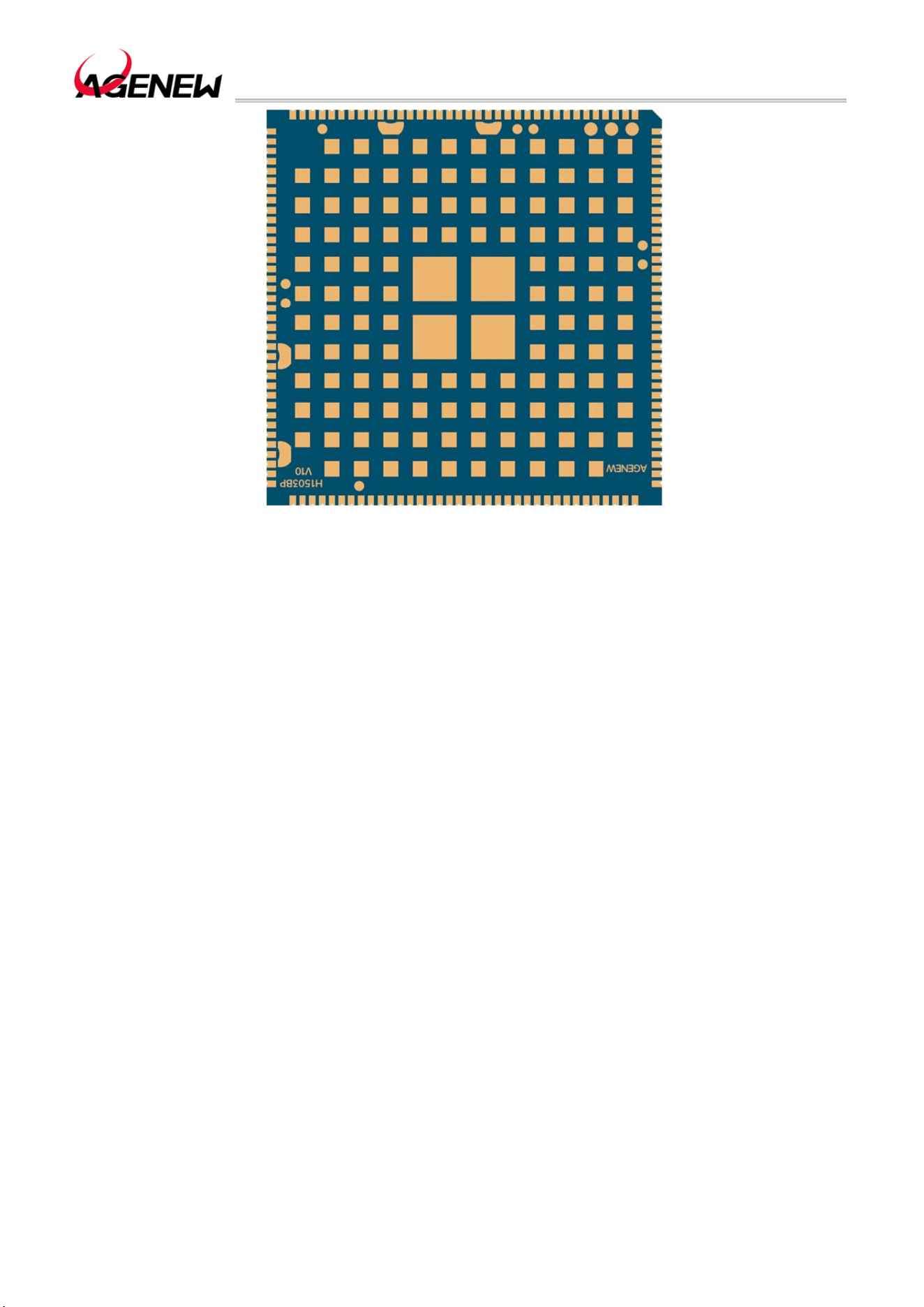
H1503BQ_Hardware Design Guide
WWW.AGENEWTECH.COM
83
Figure 44 Bottom View of The Module
Remark
The above is a design rendering of the H1503BQ module. For more accurate product
appearance and label information, please refer to the physical module of Agenewtech.

H1503BQ_Hardware Design Guide
WWW.AGENEWTECH.COM
84
9 Storage, Production and Packaging
9.1 Storage
H1503BQ Shipped in vacuum-sealed bags. The module has a humidity sensitivity level
of 3 (MSL 3) and its storage must meet the following conditions:
When the ambient temperature is below 40 degrees Celsius and the air humidity is below
90%, the components can be stored in a vacuum-sealed bag for 12 months.
After the vacuum-sealed bag is opened, the module can be directly reflowed or other
high-temperature processes if the following conditions are met:
⚫ The humidity of the air stored in the module is less than 10%.
⚫ The ambient temperature of the module is less than 30 degrees Celsius, the air
humidity is less than 60%, and the factory can complete the placement within 168 hours.
The module needs to be baked before placement if it is:
⚫ At an ambient temperature of 23 degrees Celsius (5 degrees Celsius fluctuations are
allowed), the humidity indicator card shows that the humidity is greater than 10%.
⚫ When the vacuum-sealed bag is opened, the ambient temperature of the module is
below 30 degrees Celsius, and the air humidity is less than 60%. Patches are completed in a
few hours
For the module to bake, bake at 120 degrees Celsius (allowing 5 degrees Celsius
fluctuations) for 8 hours.
Remark
The packaging of the module cannot withstand high temperature baking. Therefore,
remove the module packaging before the module bakes. If only a short baking time is required,
refer to the IPC/JEDECJ-STD-033 specification.
9.2 Production Welding
In order to ensure the quality of the module printing paste, the thickness of the stencil
corresponding to the pad part of the H1503BQ module is recommended to be
0.18mm~0.20mm. LGA pads, it is recommended to reduce the amount of solder paste to
avoid short circuits. Please refer to the documentation for details.
The recommended reflow temperature is 240ºC~245ºC, and the maximum should not
H1503BQ_Hardware Design Guide
WWW.AGENEWTECH.COM
85
exceed 245ºC. In order to avoid damage to the module due to repeated heating, it is highly
recommended that customers reflow the first side of the PCB before attaching the module.
The recommended furnace temperature curve (lead-free SMT reflow soldering) and related
parameters are shown in the chart below
Figure 45 Recommended Reflow Temperature Profile
Table 46 Recommended Furnace Temperature Test Control Requirements
Project Recommended Values
Endothermic Zone (Immersion Zone)
Maximum ramp of temperature rise 1°C /sec ~ 3°C /sec
Constant temperature time (time between A and B:
150°C~200°C period)
60 sec ~ 120 sec
Reflow Soldering Zone (Reflow Zone)
Maximum ramp of temperature rise 2°C sec ~ 3°C /sec
Reflux time (D: period over 220°C) 40 sec ~ 60 sec
Maximum temperature 240°C ~ 245°C
Cooling slope 1°C /sec ~ 4°C /sec
Number of Reflows
H1503BQ_Hardware Design Guide
WWW.AGENEWTECH.COM
86
Maximum number of reflows 1 time
9.3 Packaging
H1503BQ modules are packed in trays and sealed with anti-static bags. It is
recommended to open the package before actual production and use. Each pallet contains
20 H1503BQ modules. The specific specifications are as follows:
Figure 46 Pallet Size (mm)

H1641XO_Hardware Design Manual
WWW.AGENEWTECH.COM
87
10 Appendix A
Table 47 Abbreviations for Terms
Technical Terms Description
ADC Analog-to-digital converters
AMR Adaptive multi-rate
bps Bits per second
CS Coding schemes
CSD Circuit-switched data
CTS Clear sending
DRX Intermittent reception
EFR Enhance full rate
EGSM Extended GSM900 bands (including standard GSM900 bands)
ESD Electrostatic discharge
FRI Full rate
GMSK Gaussian minimum shift keying
GPS global positioning system
GPU Graphics Processing Unit
GSM Global System for Mobile Communications
HR Half rate
HSDPA High-speed downlink packet access

H1641XO_Hardware Design Manual
WWW.AGENEWTECH.COM
88
HSPA High-speed packet access
I/O Input and output
IQ In-phase and orthogonal
LCD LCD
LCM LCD module
LED Light-emitting diodes
LNA Low noise amplifier
LRA Linear resonant actuators
MIPI Mobile Industry Processor Interface
PCB Printed circuit boards
PDU Protocol Data Unit
PMI Power management interface
PMU Power management unit
PSK Phase-shift keying
QAM Quadrature amplitude modulation
QPSK Quadrature phase shift keying
RF rf
RTC Real-time clock chips
Rx reception
SMS Short message service
IN Terminal
TX Transmission direction

H1641XO_Hardware Design Manual
WWW.AGENEWTECH.COM
89
UART Universal asynchronous receivers and transmitters
UMTS Universal mobile communication system
YES User identification card
Vmax Maximum voltage value
Vnorm Normal voltage value
Vmin Minimum voltage value
WE Voltage input
VIHmax Maximum input high voltage value
INAUGURATION Minimum input high voltage value
VILmax Maximum input low voltage value
VILmin Minimum input low voltage value
VImax Absolute maximum input voltage value
VImin The absolute minimum input voltage value
VO Voltage output
VOHmax The maximum output high voltage value
VOHmin Minimum output high voltage value
VOLmax The maximum output low voltage value
VOLmin Minimum output low voltage value
WCDMA Wideband code division multiple access technology

FCC Statement
This device complies with part 15 of the FCC Rules. Operation is subject to the following two
conditions:
(1) This device may not cause harmful interference, and
(2) this device must accept any interference received, including interference that may cause undesired
operation.
Any Changes or modifications not expressly approved by the party responsible for compliance could void
the user's authority to operate the equipment.
The modular can be installed or integrated in mobile or fix devices only. This modular cannot be
installed in any portable device.
Any company of the host which install this modular with Single modular approval should perform the test
of radiated emissionand spurious emission according to FCC part 15C : 15.247 and 15.209 requirement,
Only if the test result comply with FCC part 15C : 15.247 and 15.209 requirement, then the host can be
sold legally.
FCC Radiation Exposure Statement
This modular complies with FCC RF radiation exposure limits set forth for an uncontrolled
environment. This transmitter must not be co-located or operating in conjunction with any other
antenna or transmitter. This modular must be installed and operated with a minimum distance of 20 cm between
the radiator and user body.
Note: This equipment has been tested and found to comply with the limits for a Class B digital
device, pursuant to part 15 of the FCC Rules. These limits are designed to provide reasonable
protection against harmful interference in a residential installation. This equipment generates
uses and can radiate radio frequency energy and, if not installed and used in accordance with the
instructions, may cause harmful interference to radio communications. However, there is no
guarantee that interference will not occur in a particular installation. If this equipment does
cause harmful interference to radio or television reception, which can be determined by turning
the equipment off and on, the user is encouraged to try to correct the interference by one or
more of the following measures:
-Reorient or relocate the receiving antenna.
-Increase the separation between the equipment and receiver.
-Connect the equipment into an outlet on a circuit different from that to which the receiver is
connected.
-Consult the dealer or an experienced radio/TV technician for help.

OEM INTEGRATION INSTRUCTIONS:
This device is intended only for OEM integrators under the following conditions:
The module must be installed in the host equipment such that 20 cm is maintained between the antenna
and users, and the transmitter module may not be co-located with any other transmitter or antenna. The
module shall be only used with the internal on-board antenna that has been originally tested and certified
with this module. External antennas are not supported. As long as these 3 conditions above are met,
further transmitter test will not be required.
However, the OEM integrator is still responsible for testing their end-product for any additional compliance
requirements required with this module installed (for example, digital device emissions, PC peripheral
requirements, etc.). The end-product may need Verification testing, Declaration of Conformity testing, a
Permissive Class II Change or new Certification. Please involve a FCC certification specialist in order to
determine what will be exactly applicable for the end-product.
Validity of using the module certification:
In the event that these conditions cannot be met (for example certain laptop configurations or co-location
with another transmitter), then the FCC/IC authorization for this module in combination with the host
equipment is no longer considered valid and the FCC ID/IC of the module cannot be used on the final
product. In these circumstances, the OEM integrator will be responsible for re-evaluating the end product
(including the transmitter) and obtaining a separate FCC authorization. In such cases, please involve a
FCC/IC certification specialist in order to determine if a Permissive Class II Change or new Certification is
required.
Upgrade Firmware:
The software provided for firmware upgrade will not be capable to affect any RF parameters as certified
for the FCC/IC for this module, in order to prevent compliance issues.
End product labeling:
This transmitter module is authorized only for use in device where the antenna may be installed such that
20 cm may be maintained between the antenna and users. The final end product must be labeled in a
visible area with the following: “Contains FCC ID: 2BVA8-H1503BQ”.
Information that must be placed in the end user manual:
The OEM integrator has to be aware not to provide information to the end user regarding how to install
or remove this RF module in the user's manual of the end product which integrates this module. The end
user manual shall include all required regulatory information/warning as show in this manual.
2.2 List of applicable FCC rules
List the FCC rules that are applicable to the modular transmitter. These are the rules that specifically
establish the bands of operation, the power, spurious emissions, and operating fundamental frequencies.

DO NOT list compliance to unintentional-radiator rules (Part 15 Subpart B/ICES-003) since that is not a
condition of a module grant that is extended to a host manufacturer. See also Section 2.10 below
concerning the need to notify host manufacturers that further testing is required.
Explanation: This module meets the requirements of FCC part 15C(15.247), FCC part 15E(15.407).
2.3 Summarize the specific operational use conditions
Describe use conditions that are applicable to the modular transmitter, including for example any limits
on antennas, etc. For example, if point-to-point antennas are used that require reduction in power or
compensation for cable loss, then this information must be in the instructions. If the use condition
limitations extend to professional users, then instructions must state that this information also extends
to the host manufacturer’s instruction manual. In addition, certain information may also be needed, such
as peak gain per frequency band and minimum gain, specifically for master devices in 5 GHz DFS bands.
Explanation: The EUT is Spring antenna.
2.4 Limited module procedures
If a modular transmitter is approved as a “limited module,” then the module manufacturer is responsible
for approving the host environment that the limited module is used with. The manufacturer of a limited
module must describe, both in the filing and in the installation instructions, the alternative means that
the limited module manufacturer uses to verify that the host meets the necessary requirements to
satisfy the module limiting conditions.
A limited module manufacturer has the flexibility to define its alternative method to address the
conditions that limit the initial approval, such as: shielding, minimum signaling amplitude, buffered
modulation/data inputs, or power supply regulation. The alternative method could include that the
limited module manufacturer reviews detailed test data or host designs prior to giving the host
manufacturer approval.
This limited module procedure is also applicable for RF exposure evaluation when it is necessary to
demonstrate compliance in a specific host. The module manufacturer must state how control of the
product into which the modular transmitter will be installed will be maintained such that full
compliance of the product is always ensured. For additional hosts other than the specific host
originally granted with a limited module, a Class II permissive change is required on the module grant
to register the additional host as a specific host also approved with the module.
Explanation: The Module is not a limited module.
2.5 Trace antenna designs
For a modular transmitter with trace antenna designs, see the guidance in Question 11 of KDB
Publication 996369 D02 FAQ – Modules for Micro-Strip Antennas and traces. The integration information
shall include for the TCB review the integration instructions for the following aspects: layout of trace
design, parts list (BOM), antenna, connectors, and isolation requirements.
a) Information that includes permitted variances (e.g., trace boundary limits, thickness, length,
width, shape(s),
dielectric constant, and impedance as applicable for each type of antenna);
b) Each design shall be considered a different type (e.g., antenna length in multiple(s) of frequency,the
wavelength, and antenna shape (traces in phase) can affect antenna gain and must be considered); c)
The parameters shall be provided in a manner permitting host manufacturers to design the printed
circuit (PC) board layout;
d) Appropriate parts by manufacturer and specifications;

e) Test procedures for design verification; and
f) Production test procedures for ensuring compliance.
The module grantee shall provide a notice that any deviation(s) from the defined parameters of the
antenna trace, as described by the instructions, require that the host product manufacturer must notify
the module grantee that they wish to change the antenna trace design. In this case, a Class II permissive
change application is required to be filed by the grantee, or the host manufacturer can take responsibility
through the change in FCC ID (new application) procedure followed by a Class II permissive change
application.
Explanation: Yes, The module with Spring antenna designs, and This manual has been shown the layout
of trace design, antenna, connectors, and isolation requirements.
2.6 RF exposure considerations
It is essential for module grantees to clearly and explicitly state the RF exposure conditions that permit a
host product manufacturer to use the module. Two types of instructions are required for RF exposure
information: (1) to the host product manufacturer, to define the application conditions (mobile, portable
– xx cm from a person’s body); and (2) additional text needed for the host product manufacturer to
provide to end users in their end-product manuals. If RF exposure statements and use conditions are not
provided, then the host product manufacturer is required to take responsibility of the module through a
change in FCC ID/IC (new application).
Explanation: This module complies with FCC RF radiation exposure limits set forth for an uncontrolled
environment, This equipment should be installed and operated with a minimum distance of 20
centimeters between the radiator and your body." This module is designed to comply with the FCC
statement, “Contains Transmitter Module FCC ID: 2BVA8-H1503BQ Or Contains FCC ID:
2BVA8-H1503BQ”.
2.7 Antennas
A list of antennas included in the application for certification must be provided in the instructions. For
modular transmitters approved as limited modules, all applicable professional installer instructions must
be included as part of the information to the host product manufacturer. The antenna list shall also
identify the antenna types (monopole, PIFA, dipole, etc. (note that for example an “omni-directional
antenna” is not considered to be a specific “antenna type”)).
For situations where the host product manufacturer is responsible for an external connector, for example
with an RF pin and antenna trace design, the integration instructions shall inform the installer that
unique antenna connector must be used on the Part 15 authorized transmitters used in the host product.
The module manufacturers shall provide a list of acceptable unique connectors.
Explanation: The EUT has a Dipole antenna, and the antenna utilizes an RA-SMA connector, making it
difficult to replace.
Brand
Model Name
Antenna Type
Connector
Gain (dBi)
Note
agenew
H1503BQ
Spring
N/A
2.4G:0.5
5G:1.2
GSM850: -1.0
GSM 1900: 0.8
2400-2500MHz
5150-5900MHz
GSM850: 824-849 MHz
GSM1900: 1850-1910 MHz

WCDMA B2: 0.8
WCDMA B:4: 0.8
WCDMA B5: -1.1
LTE B2: 0.8
LTE B4: 0.8
LTE B5: -1.1
LTE B7: 1.2
LTE B12: -2.1
LTE B13: -1.4
LTE B17: -2.1
LTE B25: 0.8
LTE B26:-1.1
LTE B41 1.2
LTE B66: 0.2
LTE B71:-2.5
WCDMA B2: 1850-1910 MHz
WCDMA B5: 824-849 MHz
WCDMA B4: 1710-1755 MHz
LTE Band 2:1850~1910MHz
LTE Band 4:1710~1755MHz
LTE Band 5:824~849MHz
LTE Band 7:2500~2570MHz
LTE Band 12:699~716MHz
LTE Band 13:777~787MHz
LTE Band 17: 704-716 MHz
LTE Band 25:1850~1915MHz
LTE Band 26 Part 90:814~824MHz
LTE Band 26 Part 22:824-849 MHz
LTE Band 41: 2496-2690MHz
LTE Band 66:1710~1780MHz
LTE Band 71: 663-698 MHz
2.8 Label and compliance information
Grantees are responsible for the continued compliance of their modules to the FCC/IC rules. This
includes advising host product manufacturers that they need to provide a physical or e-label stating
“Contains FCC ID” with their finished product. See Guidelines for Labeling and User Information for RF
Devices – KDB Publication 784748.
Explanation: The host system using this module, should have label in a visible area indicated the
following texts: “Contains Transmitter Module FCC ID: 2BVA8-H1503BQ Or Contains FCC ID:
2BVA8-H1503BQ”.
2.9 Information on test modes and additional testing requirements5
Additional guidance for testing host products is given in KDB Publication 996369 D04 Module Integration
Guide. Test modes should take into consideration different operational conditions for a stand-alone
modular transmitter in a host, as well as for multiple simultaneously transmitting modules or other
transmitters in a host product.
The grantee should provide information on how to configure test modes for host product evaluation for
different operational conditions for a stand-alone modular transmitter in a host, versus with multiple,
simultaneously transmitting modules or other transmitters in a host.
Grantees can increase the utility of their modular transmitters by providing special means, modes, or
instructions that simulates or characterizes a connection by enabling a transmitter. This can greatly
simplify a host manufacturer’s determination that a module as installed in a host complies with FCC/IC
requirements.

Explanation: Top band can increase the utility of our modular transmitters by providing instructions that
simulates or characterizes a connection by enabling a transmitter.
2.10 Additional testing, Part 15 Subpart B/ICES-003 disclaimer
The grantee should include a statement that the modular transmitter is only FCC authorized for the
specific rule parts (i.e., FCC/IC transmitter rules) listed on the grant, and that the host product
manufacturer is responsible for compliance to any other FCC/IC rules that apply to the host not covered
by the modular transmitter grant of certification. If the grantee markets their product as being Part 15
Subpart B/ICES-003 compliant (when it also contains unintentional-radiator digital circuity), then the
grantee shall provide a notice stating that the final host product still requires Part 15 Subpart B/ICES-003
compliance testing with the modular transmitter installed.
Explanation: The module without unintentional-radiator digital circuity, so the module does not require
an evaluation by FCC Part 15 Subpart B. The host shoule be evaluated by the FCC Subpart B.