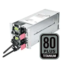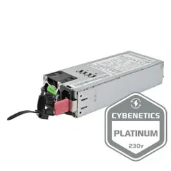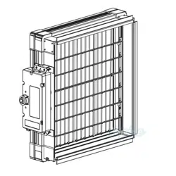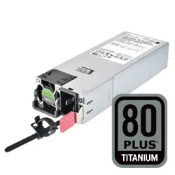

Gemini 2000C Titanium Module
Gemini Series
2000W Replacement Module for Gemini 2000C Titanium
(SST-GM2000C-TF)
●PSU For Silverstone CRPS 2000W Switching Power Supply SST-GM2000C-TF
●1U height with CRPS form factor: 73.5mm (W) x 39mm (H) x 185mm (D)
●Active PFC (full range) with 80PLUS Titanium certification
●All Japanese electrolytic capacitors, polymer capacitors and support PMBus 1.2
●Hot-swappable design with convenient pull-out handle bars
●Cold Redundancy support
●Smart Ride Through that Allow the system to quickly obtain SMBAlert signals
●Supports High Voltage Direct Current (HVDC) input up to 310VDC.
●12.2V Main Output and 12V Standby Output
●3 A max standby output current

SPECIFICATION
SilverStone Gemini Series
Gemini 2000C Titanium Module
SST-GM2000C-TFU
CRPS AC to DC Power Supply
80PLUS Titanium efficiency certified.
2000W
01
1.GENERAL SCOPE
This specification describes the performance characteristic of a 2000W
off-line modular, hot pluggable, dual output of +12.2V and +12Vsb redundant
power supply. The power supply may be used in a non-redundant, single unit
or N+M(N+M≤4) redundant configuration. The power supply shall be totally
self-contained with internal fan(s) for force air-cooling.
1.1.Mechanical Overview
The physical size of the power supply enclosure is 73.5mm x 39mm x
185mm (WxHxL). The input voltage inserts directly into the external face of
the power supply.
1.2.DC outputs, Signal outputs, Control inputs
1.2.1.Card Edge Output Connector
The output connector shall be a card-edge extension of the PC board internal
to the power supply and shall blind mate with a P36 + S14 position, (P18+S7
each side), top and bottom of card edge receptacle.
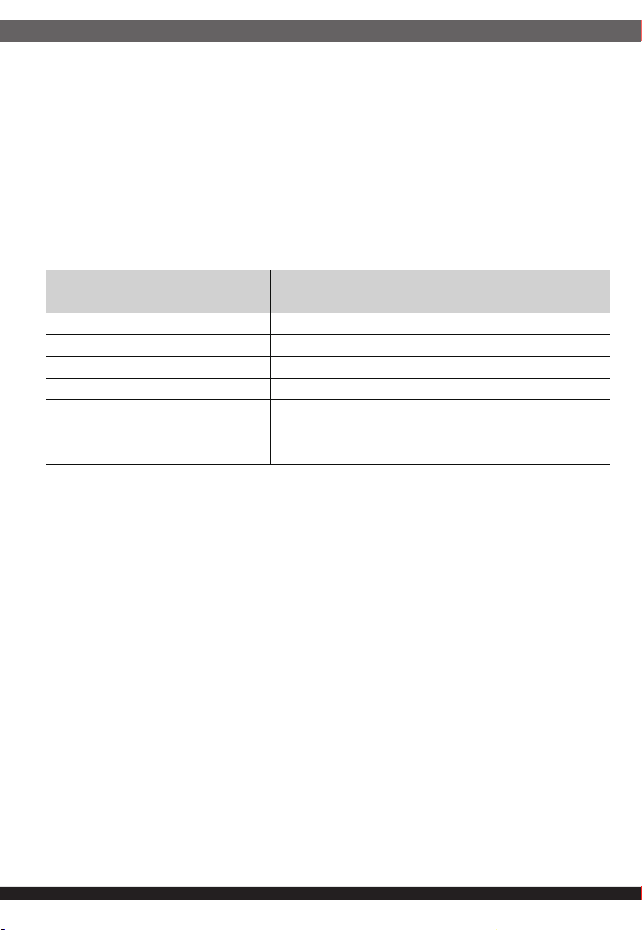
Pin number assignment relates to the card edge finger position as shown in
Table 2-1. Card edge fingers are dimensioned and numbered according to
the details shown in Figure 2-1/2-2.
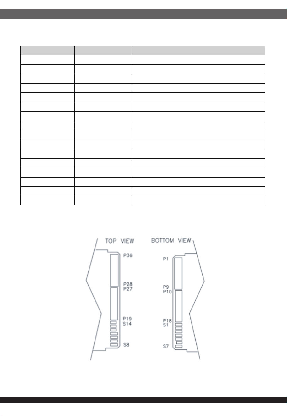
Table 2-1 – Output Connector Description
Figure 2-1 – Top view Output connector
Figure 2-2 – Bottom view Output connector
02
Pins Function Description
P1-P9, P28-P36 GND Main Return and Standby Return
P10-P18, P19-P27 +12.2V +12.2V Main output
S1 A0 Address pin 0
S2 A1 Address pin 1
S3 +12VSB 12V standby output
S4 C_R Cold Redundancy
S5 +12VLS +12V Load share bus
S6 PRESENT Power supply present signal
S7 INPUT_OK Input voltage ok signal
S8 PW_OK Output voltage OK signal
S9
+VSENCE
+12V Remote Sense
S10
-VSENCE
12V standby Return sense.
S11 SMB_Alert
#
PS Alert signal for failure notification
S12 PSON +12V output on/off control signal
S13 SCL PMBus Clock
S14 SDA PMBus Data
03
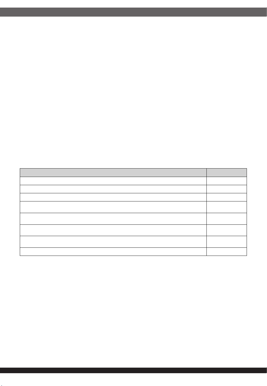
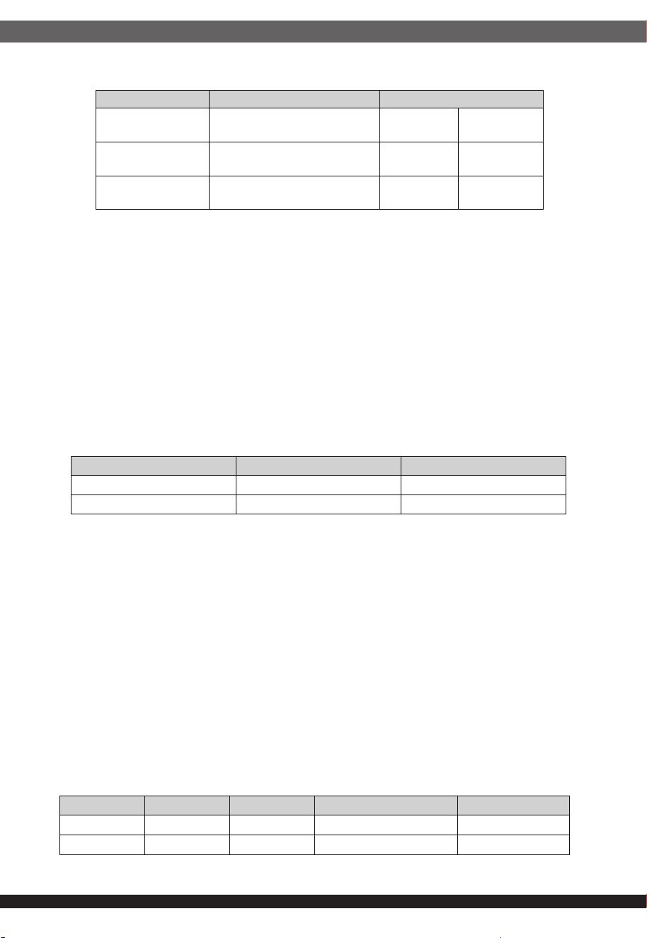
Table 2-2 – LED States Information
1.3.Handle Retention
The power supply shall have a handle to assist extraction. The module shall be
able to inserted and extracted without the assistance of tools. The power supply
shall have a latch which retains the power supply into the system and prevents
the power supply from being inserted or extracted from the system when the AC
power cord is inserted or extracted from the power supply. The handle shall
protect the operator from any burn hazard.
1.4.LED Marking and Indicator
The power supply shall use bi-colored LED (Green,Yellow) on the AC inlet side .
Table 2-2 shows the LED states for each power supply operating state, indica-
tion of the power supply status. The LED is driven by an internal circuitry and
should even illuminate in an N+M configuration even without AC power.
The LED and its location shall meet ESD requirements required for the power
supply. The LED shall be securely mounted in such a way that incidental
pressure on the LED will not cause it to become displaced.
1.5.Power Supply FAN and Orientation
Power supply shall contain one single rotor 40mm x 40mm x 28mm to cool the
power supply and provide some additional system cooling and ventilation.
The power supply’s internal design provides the option to create two airflow
directions. Internal Fan can be mounted to draw air through the power supply
with inlet air being pulled in through the DC output face or the fan can be
mounted to push air through the power supply with exhaust air being blown out
the DC output face.
For definition of the air flow direction can rely on the eject color,
with the pull in air through the DC connector (Rear to Front, AFO), the eject
handle color is BLACK,
with the pull air through the power supply (Front to Rear, AFI), the eject color is
GREEN.
Power Supply Condition LED State
Output ON and OK Green
PSU standby state when AC present / Only 12Vsb on 1Hz Blink Green
N
o AC power to all power supplies Off
Power supply is cold standby state or always standby state as defined in the Cold Redundancy
section
1Hz Blink Green
AC cord unplugged or AC power lost; with a second power supply in parallel still with AC input
p
ower.
0.5Hz Blink Yellow
Power supply critical event causing a shutdown; failure, over current, short circuit, over voltage,
fan failure, over temperature
Yellow
Power supply warning events where the power supply continues to operate; high temp, high
p
ower, high current, slow fan.
1Hz Blink Yellow
Power supply FW updating 2Hz Blink Green
04
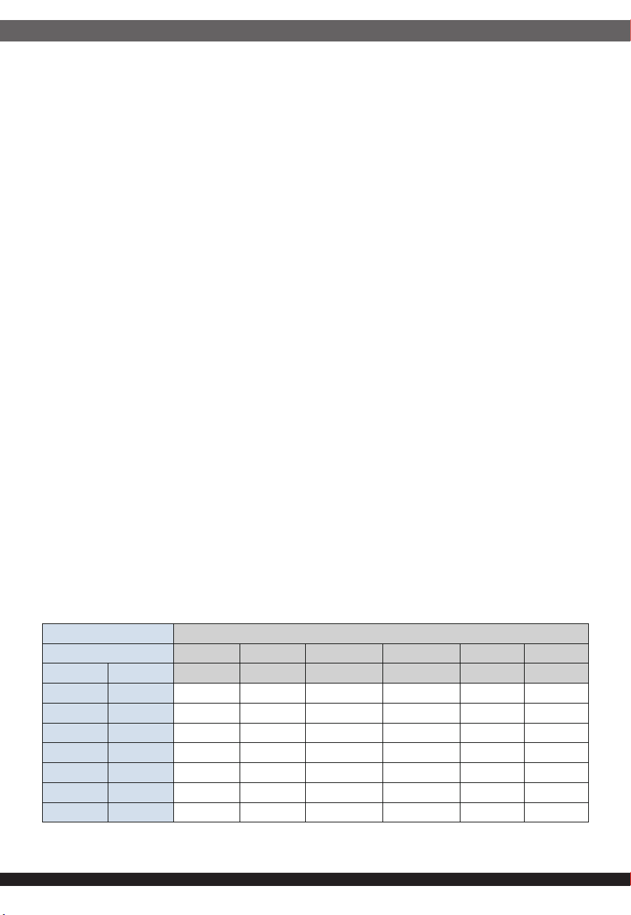
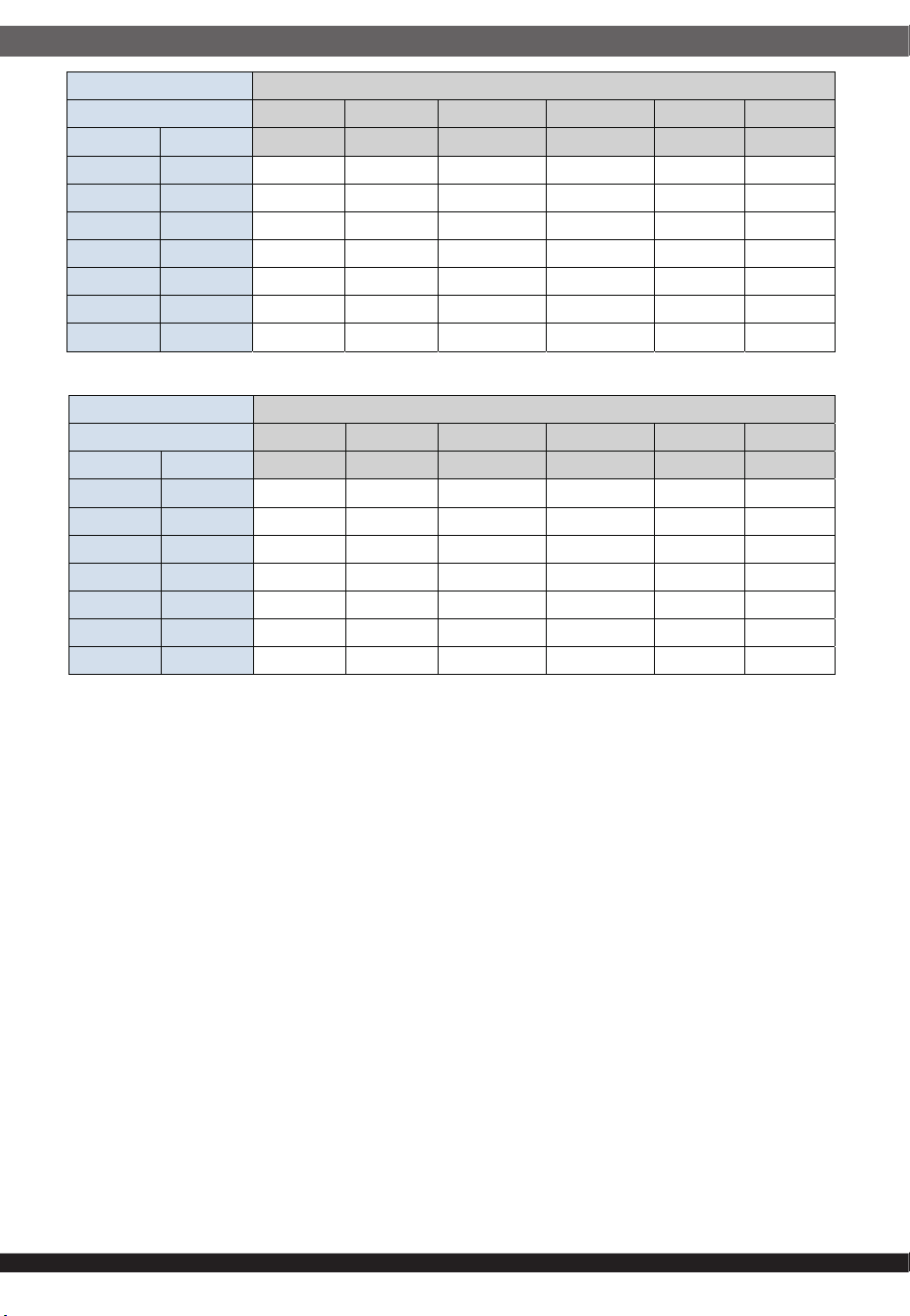
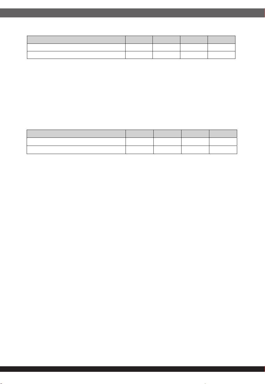
Table 2-3 – PSU airflow impedance& Acoustic level (AFO)
1.6.Airflow Requirements
The power supply shall be capable of supplying the airflow that is sufficient for
self-cooling when installed in different system airflow impedances. System may
present a negative pressure to the power supply’s airflow. The internal fan shall be
capable of providing airflow specified in Table 2-3 depending on power supply
configuration. The conditions must be satisfied under the maximum inlet tempera-
ture and altitude limits as specified in the table. All airflow shall pass through the
power supply at operating temperature and not over the exterior surfaces of the
power supply. Recommended air flow is a minimum of 16.5CFM. The system
impedances design should meet the requirements shown in table.
1.6.1.Acoustic Requirements
The power supply shall incorporate variable speed fan(s).The power supply
internal fan shall be controllable through PWM control. The fan speed shall vary
based on output loading and ambient temperature. The Fan shall also be controlla-
ble through PMBus or SMBus command.
The declared sound power level (LwAd) of the power supply must meet the
requirements shown in the Table 2-3 . Sound power must be measured according
to ECMA 74 (www.ecma-international.org) and report according to ISO 9296/I-
SO7779. The sound pressure measurement must be measured at a distance of
one meter from the face of the fan. Centered on the AC connector face of the
power supply.
Operating condition Ambient temperature condition(°C)/FAN Duty
Load current(A) Falling Rising Falling Rising Falling Rising
Rising Falling
<33°C <37°C >33°C,<42°C >37°C,<45°C >42°C >45°C
<40 <34 40% 40% 60% 60% 70% 70%
>40 >34 50% 50% 70% 70% 80% 80%
>56 >50 60% 60% 80% 80% 90% 90%
>72 >66 70% 70% 90% 90% 100% 100%
>88 >82 80% 80% 100% 100% 100% 100%
>104 >98 90% 90% 100% 100% 100% 100%
>120 >114 100% 100% 100% 100% 100% 100%
05
2.AC Input Requirement
2.1.AC Inlet Connector
The power supply shall incorporate a standard IEC 60320-1 C20 power inlet.
2.2.Input Voltage Specification
The power supply shall operate within all specified limits over the following input
range in Table
3-1. Harmonic distortions of up to 10% of the rated line voltage will not cause
the power supply to go out of specified limits.
The power supply shall power off if the AC input is below VACpower_offt and
shall start (auto recover) if VACstart_up is reached. Input of VAC is below
VACpower_off shall not cause any damage to the power supply, including the
input fuse.
The power supply shall supply the full output power in the voltage range of
90VAC to 264VAC.
Operating condition
Ambient temperature condition (°C)/ Volumetric flow, stand-alone (Min. CFM)
Load current(A) Falling Rising Falling Rising Falling Rising
Rising Falling
<33°C <37°C >33°C,<42°C >37°C,<45°C >42°C >45°C
<40 <34 6.509 6.509 9.643 9.643 11.249 11.249
>40 >34 7.747 7.747 11.249 11.249 13.223 13.223
>56 >50 9.643 9.643 13.223 13.223 14.948 14.948
>72 >66 11.249 11.249 14.948 14.948 16.5 16.5
>88 >82 13.223 13.223 16.5 16.5 16.5 16.5
>104 >98 14.948 14.948 16.5 16.5 16.5 16.5
>120 >114 16.5 16.5 16.5 16.5 16.5 16.5
Operating condition Ambient temperature condition (°C)/ Acoustic(db)
Load current(A) Falling Rising Falling Rising Falling Rising
Rising Falling
<33°C <37°C >33°C,<42°C >37°C,<45°C >42°C >45°C
<40 <34 57.8 57.8 71.3 71.3 73.6 73.6
>40 >34 65.1 65.1 73.6 73.6 78.2 78.2
>56 >50 71.3 71.3 78.2 78.2 90% 90%
>72 >66 73.6 73.6 78.8 78.8 80.9 80.9
>88 >82 78.2 78.2 80.9 80.9 80.9 80.9
>104 >98 78.8 78.8 80.9 80.9 80.9 80.9
>120 >114 80.9 80.9 80.9 80.9 80.9 80.9
06
2.2.1.HVDC Input Voltage
The power supply supports High Voltage Direct Current (HVDC) input. Allowed
HVDC input range as shown in Table 3-2. The power supply shall operate within
all specified limits when HVDC input requirements defined in this chapter.
2.2.2.240HVDC Input Voltage Polarity
IEC 60320-1 C20 power inlet may be used to connect DC input voltage to the
power supply. Table 3-3 summarizes the valid input DC connections.
Notes: The input terminals shown in Table 3-3 when marked with a (*) indicates
that they have the same input terminal connection. The GND terminal shall not
be used for power connections.
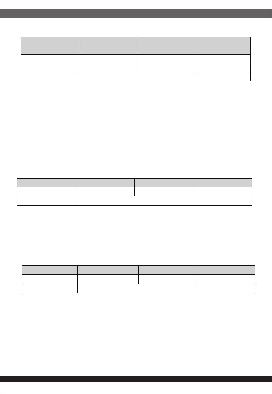
2.3.Input current
The maximum input current defines the maximum possible input current in
Table 3-4 to ensure the proper function of the power supply to meet all defined
specifications.
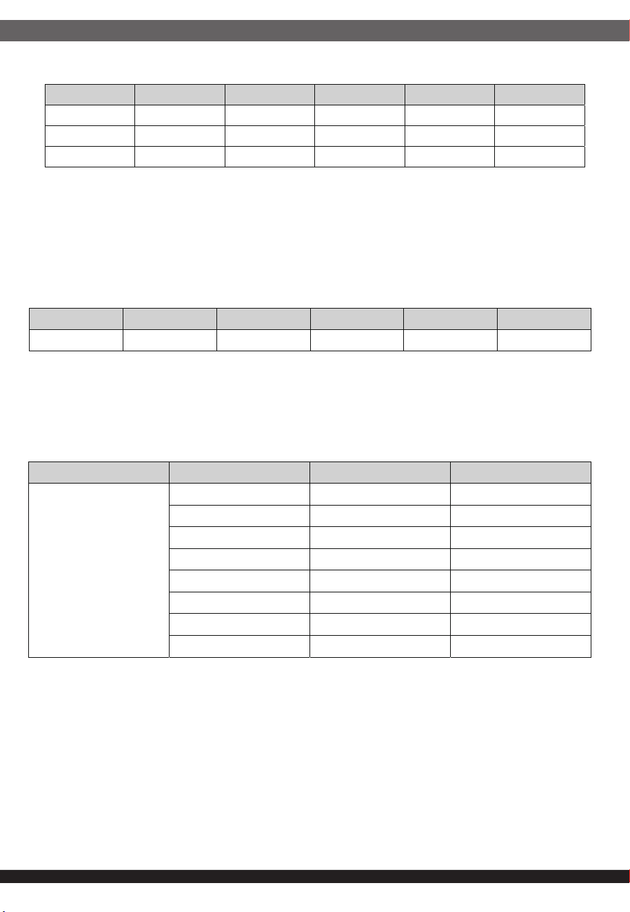
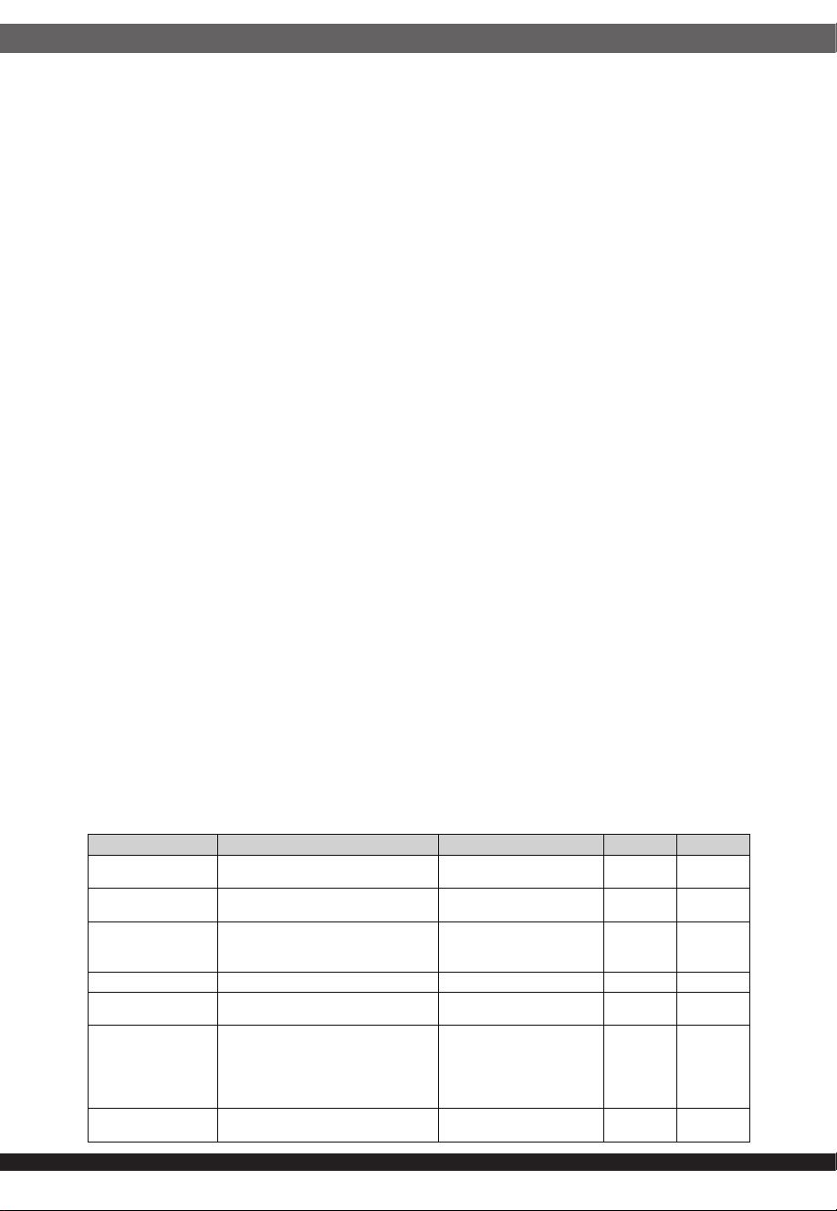
Table 3-1 – AC input voltage range
Table 3-2 – HVDC input voltage range
Table 3-3 – VALID DC input voltage connections
Parameter Min. input Rated Input Max. input Start up VAC Power off VAC
115VAC 90V
rms
100-120V
rms
132V
rms
85VAC+/-5VAC 75VAC+/-5VAC
230VAC 180V
rms
200-240V
rms
264V
rms
Frequency 47Hz 50/60Hz 63Hz
Parameter Min. input Rated Input Max. input Start up VDC Power off VDC
240VDC 190VDC
240VDC
310VDC
175V+/-5VDC 170V+/-5VDC
Input HVDC Range LINE NEURAL EARTH
190-310VDC
+VDC Return GND
+VDC Return* GND*
Return +VDC GND
Return* +VDC GND*
-VDC Return GND
-VDC Return* GND*
Return -VDC GND
Return* -VDC GND*

07
Table 3-4 – Maximum input current
2.4.Line Fuse
The PSU can support two types of input voltage ,one is AC input only ,other one
is AC compatible with HVDC , base on specific input voltage with appropriate
fuse type.
2.4.1.AC/HVDC Line Fuse (AC/HVDC)
The power supply shall incorporate one input fuse on the line side for input
over-current protection to prevent damage to the power supply and meet
product safety requirements. The input fuse shall be a fast blow fuse, which is to
meet safety certificated with AC/HVDC voltage. AC or HVDC inrush current
shall not cause the line fuse to blow under any conditions. All protection circuits
in the power supply shall not cause the AC/HVDC fuse to blow unless a compo-
nent in the power supply has failed. This includes DC output load short condi-
tions.
2.4.2.AC Line Fuse (AC input only)
The power supply shall incorporate one input fuse on the line side for input
over-current protection to prevent damage to the power supply and meet
product safety requirements. The input fuse shall be a fast blow fuse. AC inrush
current shall not cause the AC line fuse to blow under any conditions. All
protection circuits in the power supply shall not cause the AC fuse to blow
unless a component in the power supply has failed. This includes DC output
load short conditions.
2.5.AC/HVDC Line Inrush
The power supply must meet inrush requirements for any rated AC/HVDC
voltage; during turn on at any phase of AC/HVDC voltage, during a single cycle
AC dropout condition, during repetitive ON/OFF cycling of AC/HVDC, and over
the specified temperature range (TOP). The peak Inrush current shall be less
than the ratings of its critical components (including input fuse, bulk rectifiers,
and surge limiting device).
The maximum AC/HVDC line inrush current for this power has defined in below
table 3-5 over the entire input voltage range.
Input voltage Input current Max. power
100-120VAC 14A 1000W
200-240VAC 14A 2000W
240HVDC 14A 2000W
08
Table 3-5 – AC/HVDC Line inrush current definition
Table 3-6 – Power iTHD requirement
Table 3-7 – Power factor requirement
Input
Voltage
Initial Cold Start
Inrush Current
Initial Cold Start
Inrush Current
Initial Cold Start
Inrush Current
90-132 VAC 50 A for 2 μs 40 A for 200 μs 40 A for 5 ms
180-264 VAC 100 A for 2 μs 40 A for 200 μs 60 A for 5 ms
190-310 VDC 100 A for 2 μs 40 A for 200 μs 60 A for 5 ms
Notes:
1.Inrush current shall be measured at an ambient temperature of 25 degree C
after the input voltage has been removed from the power supply for a
minimum of 10 minutes.
2.The inrush current due to the EMI filter capacitors can be ignored.
2.6.iTHD and Power Factor
The power supply shall incorporate universal input with active power factor
correction which shall reduce line harmonics in accordance with EN 61000-3-2
and JEIDA MITI standards in Table 3-6.
In addition, whenever the PFC converter is ON, the power factor shall be
equal to or greater than the requirements as defined in Table 3-7. Power factor
measurements shall be performed with source impedance of less than 0.1
ohm. It is expected that the boost converter will operate at the lowest output
voltage possible to meet specification for given loading and input conditions.
2.7.AC/HVDC line dropout/Hold up
An AC/HVDC line dropout is the condition when AC/HVDC input drops below
minimum rated input voltage at any phase of the AC/HVDC line for any length
of time. During an AC/HVDC dropout of one half cycles or less, the power
supply shall meet the dynamic voltage regulation limits defined in section 4.4
over 100% of the rated load. An AC/HVDC line dropout of one half cycles or
less shall not cause malfunction of control signals or protection circuits.
Output power ≥ 20% ≥ 50% 100%
Current iTHD ≤15% ≤10% ≤10%
Input conditions 115VAC to 230VAC & 50Hz / 60Hz
Output power 20% load 50% load 100% load
Power factor > 0.95 > 0.98 > 0.99
Input conditions 200VAC to 240VAC & 50Hz / 60Hz
09
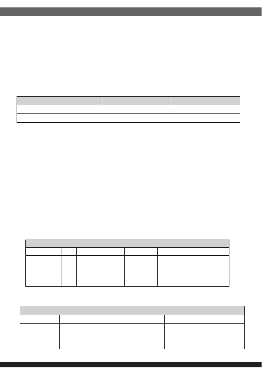
Table 3-8 – AC Hold-up /Dropout
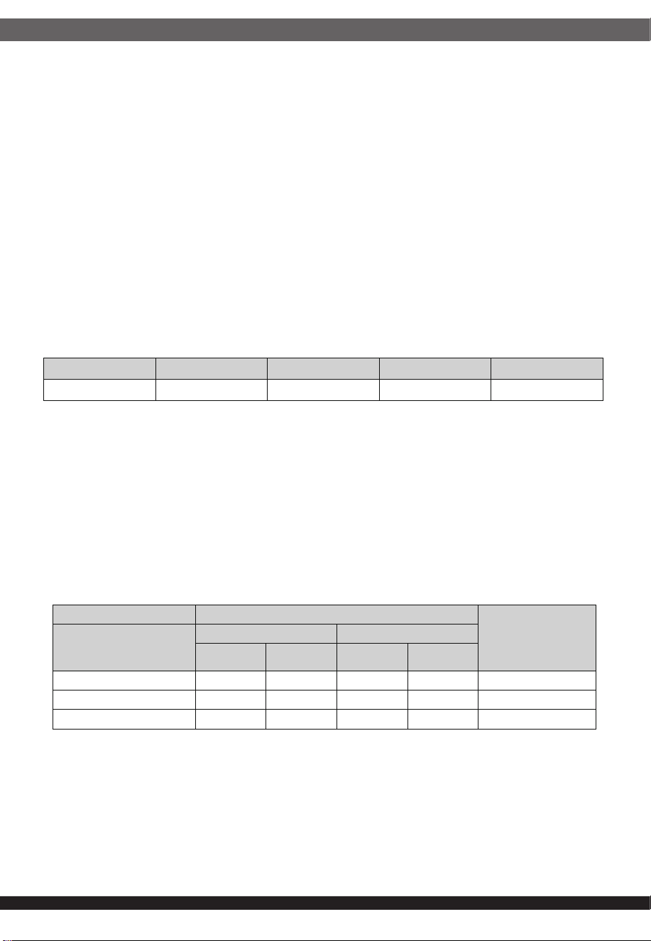
Table 3-9 – AC Line SAG transient performance.
Table 3-10 – AC Line SURGE transient performance.
AC/HVDC line dropout of any duration shall not cause tripping of control signals
or protection circuits other than the SMB_Alert# signal. If the AC/HVDC dropout
time is long enough such that the power supply shuts down, the power supply
shall recover safely and meet all turn on requirements. The power supply shall
meet the AC/HVDC dropout requirement over rated AC/HVDC input voltages,
frequencies, and output loading conditions. Any dropout of the AC/HVDC line
shall not cause damage to the power supply . The input ok signal shall indicate
when AC/HVDC input is valid as defined in section 5.4.
The +12Vsb output voltage shall stay in regulation under its full load(static or
dynamic) during an AC/HVDC dropout duration up to 70ms whether the power
supply is in ON or OFF state (PSON# asserted or de-asserted).
2.8.AC Line Transient Specification
AC line transient conditions shall be defined as “sag” and “surge” conditions.
“Sag” conditions are also commonly referred to as “brownout”, these conditions
will be defined as the AC line voltage dropping below nominal voltage condi-
tions.
“Surge” will be defined to refer to conditions when the AC line voltage rises
above nominal voltage.
The power supply shall meet the requirements under the following AC line sag
and surge conditions.
Loading during AC dropout/Holdup Main output Standby output
100% 6ms 70ms
70% 10ms 70ms
AC Line Sag (10sec interval between each sagging)
Duration Sag Operating AC voltage Line frequency Performance criteria
0 to 1/2 AC cycle 95% Nominal AC voltage 50/60Hz
Loss of function acceptable,
self- recoverable.
>1 AC cycles >30% Nominal AC voltage 50/60Hz
Loss of function acceptable,
self- recoverable.
AC Line Surge
Duration Surge Operating ac voltage Line frequency Performance criteria
Continuous 10% Nominal AC voltage 50/60Hz No loss of function or performance.
0 to 1/2 AC cycle 30%
mid-point of nominal AC
voltage
50/60Hz No loss of function or performance.
10
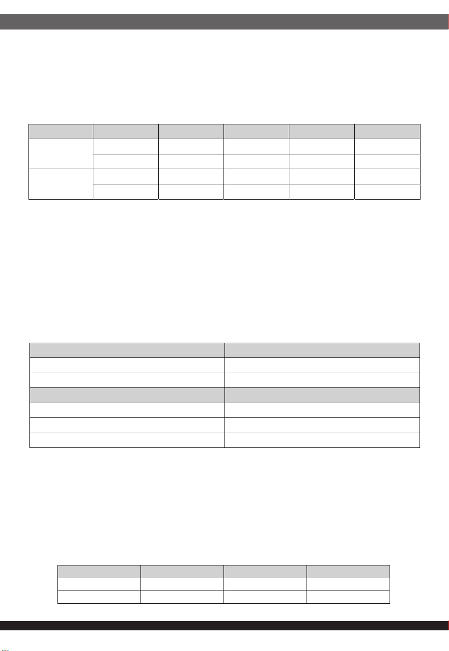
Table 3-11 – Efficiency Requirements
Table 4-1 – Output Power/ Current Ratings
2.9.Power Recovery
The power supply shall recover automatically after an AC power failure. AC
power failure is defined to be any loss of AC power that exceeds the dropout
criteria.
2.10.AC Line Leakage Current
The maximum leakage current to ground for each power supply module shall
not exceed 1.75mA when tested at 240Vac/60Hz.
Note:
When the touch current over 5mA in system application, such as N+M configu-
ration, system side could follow IEC 62368-1” Equipment with touch current
exceeding 5mA” section to get safety approval.
2.11. Efficiency
3.DC Output Specification
3.1.Output Power/Currents
The following Table 4-1 defines the power and current rating of the 2000W
power supply. The combined output power of all outputs shall not exceed the
rated output power. The power supply must meet both static and dynamic
voltage regulation requirements.
3.2.Auxiliary Output (Standby)
The +12Vsb output shall be present when an AC/HVDC input greater than the
power supply turn on voltage is applied. There should be load sharing in the
standby rail.
3.3.No load operation
The power supply shall meet all requirements except for the transient loading
requirements when operated at no load on all outputs.
Loading 10% of maximum 20% of maximum 50% of maximum 100% of maximum
Titanium efficiency 90% 94% 96% 91%
Input Voltage Outputs
Combined Max.
Output Power(W)
Range
+12Vsb +12.2V
Minimum
Current(A)
Maximum
Current(A)
Minimum
Current(A)
Maximum
Current(A)
90-132VAC 0 3 1 82 1000W
180-264VAC 0 3 1 164 2000W
190-310HVDC 0 3 1 164 2000W
11
3.4.Voltage Regulation
The power supply shall meet the Voltage regulation under all operating conditions
(AC/HVDC line, transient loading, output loading). These limits include the
peak-peak ripple/noise. The regulation of Table 4-2 shall be measured at the
output connector of the power supply.
3.5.Ripple and Noise Regulation
Ripple and Noise is defined in Table 4-3. Ripple and Noise shall be measured
over a Bandwidth of 10Hz to 20MHz at the power supply output connector. A
high frequency 0.1μF ceramic capacitor and 10μF of tantalum capacitor shall
be placed at each point of measurement. The measurement points shall be as
close as possible to the point of load. To help reduce switching ripple further,
an additional 6,600μF low ESR electrolytic capacitor may be placed in parallel.
The ripple and noise specification shall be meet over all load ranges and
AC/HVDC line voltages with N+M power supplies in parallel operation.
3.6.Dynamic loading
The output voltage shall remain within limits specified for the step loading and
capacitive loading specified in Table 4-4.
The load transient repetition rate shall be tested between 50Hz to 5kHz at duty
cycles ranging from 10%-90%. The load transient repetition rate is only a test
specification. The Δ step load may occur anywhere within the minimum load to
the peak load condition.
Table 4-2 – Output Voltage regulation limits
Table 4-3 – Ripple and Noise Regulation
Table 4-4 – Transient Load Requirements
Note: For dynamic conditions +12.2V min loading is 3A.
PSU Status Output Minimum Nominal Maximum Tolerance
Static
+12.2V 11.834V 12.2V 12.566V +/-3%
+12Vsb 11.64V 12.0V 12.36V +/-3%
Dynamic
+12.2V 11.59V 12.2V 12.81V +/-5%
+12Vsb 11.4V 12.0V 12.6V +/-5%
Output Voltage Ripple/Noise pk-pk
+12.2V 120mV
+12Vsb 120mV
Signals Ripple/Noise pk-pk
PWOK 400mV
PSON 400mV
SMB_Alert
#
400mV
Output Δ Step load size Load Slew Rate Test Capacitive Load
+12.2V 60% of Max. 0.5A/μs 2,200μF
+12Vsb 1.0A 0.5A/μs 100μF

12
Table 4-5 – Capacitive Loading Conditions
3.7.Capacitive loading
The power supply shall be stable and meet all requirements with the following
capacitive loading ranges defined in below Table 4-5
3.8.Closed loop stability
The power supply shall be unconditionally stable under all line/load/transient load
conditions including capacitive load ranges. A minimum of: 45 degrees Phase
Margin and -10dB Gain Margin is required.
Closed-loop stability must be ensured at the maximum and minimum loads as
applicable.
3.9.Grounding
The output ground of the pins of the power supply provides the output power
return path. The output connector ground pins shall be connected to the safety
ground (power supply enclosure). This grounding should be well designed to
ensure passing the max allowed Common Mode Noise levels.
The power supply shall be provided with a reliable protective earth ground. All
secondary circuits shall be connected to protective earth ground. Resistance of
the ground returns to chassis shall not exceed 0.1Ω. This path may be used to
carry DC-current not exceed 32A.
3.10.Soft starting
The power supply shall contain control circuit which provides monotonic soft start
for its outputs without overstress of the AC/HVDC line or any power supply
components at any specified AC/HVDC line or load condition.
3.11.Residual Voltage Immunity in Standby mode
The power supply should be immune to any residual voltage placed on its outputs
(typically a leakage voltage through the system from standby output) up to
100mV. There shall be no additional heat neither generated nor stressing of any
internal components with this voltage applied to any individual or all outputs
simultaneously. It also should not trip the protection circuits during turn on/off.
The residual voltage at the power supply outputs for no load condition shall not
exceed 100mV when AC/HVDC voltage is applied and the PSON# signal is
de-asserted.
Output Min. Max.
+12.2V 1000μF 22,000μF
+12Vsb 100μF 2,000μF

13
3.12.Common mode noise
The Common Mode noise on any output shall not exceed 350mV pk-pk over the
frequency bandwidth of 10Hz to 20MHZ.
The measurement shall be made across a 100 ohm resistor between each of DC
outputs. Including ground at the DC power connector and chassis ground (power
subsystem enclosure).
3.13.Overshoot
Any output overshoot at turn on shall be less than 5% of the nominal output value.
Any overshoot shall recover to within the specified regulation in less than 0.5mS
3.14.Undershoot
Any output shall not undershoot at turn on or off cycle under any circumstances.
3.15.Temperature coefficient
After operating for 30 minutes or longer at 25° C ambient, the output voltages
shall not change by more than 0.05 % per degree C for any given line and load
conditions.
3.16.Hot Swap Requirements
Hot Swapping a power supply is the process of inserting and extracting a power
supply from an operating power system. During this process the output voltages
shall remain within the limits with the capacitive load specified.
The hot swap test must be conducted when the system is operating under static,
dynamic and zero loading conditions. The power supply shall use a latching
mechanism to prevent insertion and extraction of the power supply when the input
power cord is inserted into the power supply.
The power supply can be hot swapped by the following method:
Extraction: The power supply may be removed from the system while operating
with PSON# asserted, while in standby mode with PSON# de-asserted or with no
AC applied. No connector damage should occur during un-mating of the power
supply from the power distribution board (PDB) or system.
Insertion: The power supply may be inserted into the system with PSON# assert-
ed, with PSON# de-asserted or with no AC power present for that supply. No
connector damage should occur due to the mating of the output and input connec-
tor.
In general, a failed power supply may be removed, then replaced with a good
power supply, however, hot swap needs to work with operational as well as failed
power supplies. The newly inserted power supply will get turned on into standby
or Power On mode once inserted.
14
3.17.Load sharing control
The +12.2V output shall have active load sharing. When operating at 50% of full
load, the output current of any N+1 or N+M(N+M≤4) power supplies shall be
within (+/-10%), When operating at 20% to 49% load, the output current of any
N+1 or N+M(N+M≤4) power supplies shall be within (+/-15%). For example of 1+1
configuration, if power supply #1 is operating at 12A, then all other power supplies
within the system shall be operating between 10.8A to 13.2A (+/- 10% of 12A).
All current sharing functions shall be implemented internal to the power supply by
making use of the +12VIBUS signal. The system side or PDB must connect the
+12VIBUS signals between the power supplies together. The power supply shall
be able to share with up to N+1 or N+M supply in parallel. The failure of a power
supply shall not affect the load sharing or output voltages of the other supplies still
operating. The power supplies must be able to load share with 100mV of drop
between different power supply’s outputs.
If the load sharing is disabled by shorting the load share bus to ground, the power
supply shall continue to operate within regulation limits for loads less than or
equal to the rating of one power supply.
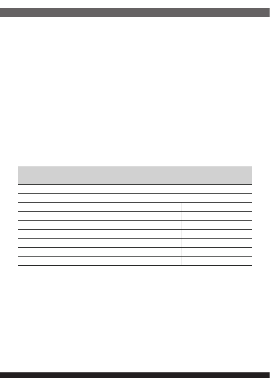
3.18.Timing Requirements
These are the timing requirements for the power supply operation. All outputs
must rise monotonically. Table 4-7 shows the timing requirements for the power
supply being turned on and off via two different ways; 1) via the AC input with
PSON held low; 2) via the PSON signal with the AC input applied.
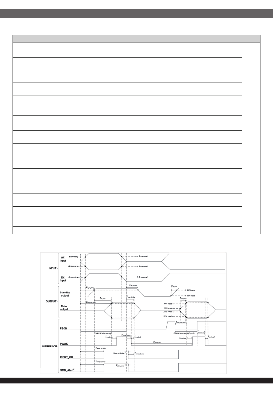
3.18.1.Output Voltage Timing
The timing of signals and outputs are specified in below Table 4-7 and illustrated
in Figure 4-1.
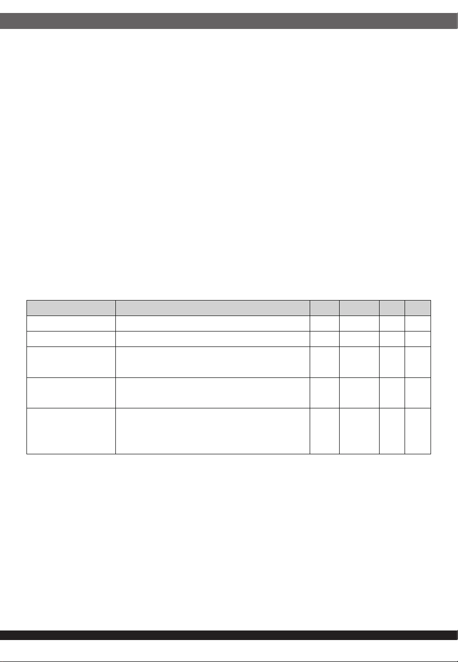
Table 4-6 – Load share bus output characteristics
Item Description Min Nominal Max Units
+12VIBUS; I
out
=164A Voltage of load share bus at 164A. 8 V
△V
share
/△I
out
Slope of load share bus voltage with changing load. 8/I
164A
V/A
I
shareSINK
Amount of current the load share bus output from each
power supply is allowed to sink.
1.5 mA
I
shareSOURCE
Amount of current the load share bus output from each
power supply needs to source.
1.5 mA
T
share
; I
out
=Max.
Delay from output voltages in regulation to load sharing
active with maximum load of one power supply and two
power supplies in parallel. (remote on/off only)
100 msec
15
Table 4-7 – Timing Requirements
Figure 4-1 – Turn On/Off Timing (Power Supply Signals)
Item Description MIN MAX UNITS
T
vout_rise
Output voltage rise time for all main output. 1 80
mS
T
sb_rise
Output voltage rise time for standby output. 1 80
T
sb_on_delay
Delay from input voltage being applied to standby voltage being within
regulation.
2,500
T
vout_on_delay
Delay from input voltage being applied to all main output voltage being
within regulation.
3,000
T
vout_holdup
Time all main output voltages stay within regulation after loss of input
voltage.
4
T
sb_holdup
Time the standby output voltage stays within regulation after loss of
input voltage.
70
T
pwok_holdup
Delay from loss of input voltage to de-assertion of PWOK. 3
T
pson_on_delay
Delay from PSON active to output voltages within regulation limit. 5 400
T
pson_pwok
Delay from PSON deactivate to PWOK being de-asserted. 5
T
pwok_on
Delay from main output voltage within regulation limits to PWOK
asserted at turn on.
100 500
T
pwok_off
Delay from PWOK de-asserted to output voltages dropping out of
regulation limits.
1
T
pwok_low
Duration of PWOK being in the de-asserted state during an off/on cycle
using Input voltage or the PSON signal.
100
T
sb_vout
Delay from standby voltage being in regulation to main output being in
regulation at input voltage turn on.
50 1,000
T
input_on_delay
Delay from input voltage applied to INPUT_OK going high during
power-up.
1,000
T
alert_on_delay
Delay from input voltage applied t o SMB_Alert
#
going high during
power-up.
1,000
T
input_ok_holdup
Timing from input voltage dropping to 0VAC to INPUT_OK going low. 4
T
input_ok_vout
Timing from INPUT_OK going low to main out put falling out of
regulation at i nput voltage turn off.
2
T
alert_input
Timing from input voltage dropping to 0V to SMBAlert
#
going low. 4
16
4.Control and Indicator functions
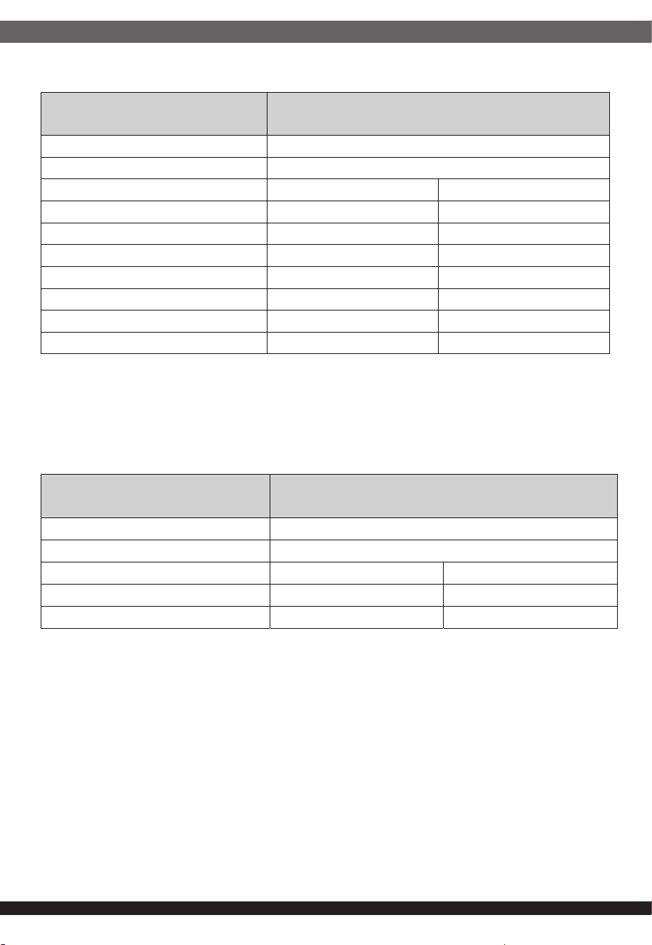
Table 5-1 – PSON# Required Signal Characteristics
The following sections define the input and output signals from the power supply.
Signals that can be defined as low true use the following convention:
Signal# = low true.
4.1.PSON# (Input Signal of Power supply enable)
The PSON# signal is required to remotely turn on/off the main output of the power
supply.
PSON# is an active low signal that turns on the 12.2V power rail. When this signal
is not pulled low by the system or left open, the outputs (except the +12Vsb) turn
off.
This signal (PSON#) is pulled to 3.3V voltage by a 2K ohm pull-up resistor internal
to the power supply.
4.2.PWOK (Power Ok) Output Signal
PWOK is a power good signal and will be pulled HIGH by the power supply to
indicate that all outputs are within regulation limits of the power supply. When any
output voltage falls below regulation limits or when AC/HVDC power has been
removed for a time sufficiently long so that power supply operation is no longer
guaranteed, PWOK will be de-asserted to a LOW state. See Table 5-2 for a
representation of the timing characteristics of PWOK. The start of the PWOK
delay time shall inhibited as long as any power supply output is in current limit.
Signal Type
Accepts an open collector/drain input from the system. Pull-up to
3.3V with 2K ohm resistor located in power supply.
PSON
#
= Low ON
PSON
#
= High or Open OFF
MIN MAX
Logic level low (power supply ON) 0V 0.8V
Logic level high (power supply OFF) 2.0V 3.46V
Source current, V
pson
= low 0.28mA
Power off delay: T
pson_off_delay
50msec
Power up delay: T
pson_on_delay
5msec 400msec
PWOK delay: T
pson_pwok
5msec
17
Table 5-2 – PWOK Signal Characteristics
4.3.INPUT_OK (Input Good Output Signal)
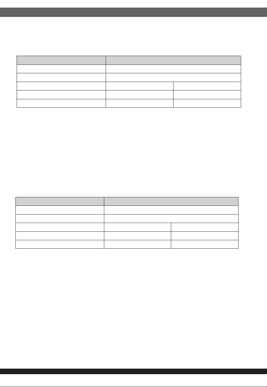
Table 5-3 – INPUT_OK signal characteristics
INPUT_OK# is an AC good signal and will be pulled up by the power supply to
indicate that AC input is within the operation range.
4.4.Present Signal (PRESENT)
This signal pin is recessed within the connector and will contact only once all
other connector contacts are closed. This active-low pin is used to indicate to a
power distribution unit controller that a supply is plugged in. the maximum current
on PRESENT# pin should not exceed 10mA. This signal has a 4.7 ohm/0.1W pull
low resistor.
4.5.A0
PSU Module Address Line 0. This signal line is provided for determining the
address for the specific PSU FRU and SMBus address. The pull-up resistor
should be located in the system and the pull-up voltage should be limited to 3.3V.
The address line should be pull low with equal to or less than 100 ohm in the
motherboard design.
Signal Type
Open collector/drain output from power supply. Pull-up to 3.3V
with 2.43K ohm resistor located in the power supply.
PWOK=High Power OK
PWOK=Low Power Not OK
MIN MAX
Logic level low voltage, I
sink
=400μA 0V 0.4V
Logic level high voltage, I
source
= 200μA 2.4V 3.46V
Sink current, PWOK=low 4mA
Source current, PWOK=high 0.2mA
PWOK delay: T
pwok_on
100msec 500msec
PWOK rise and fall time 100μsec
Power down delay: T
pwok_off
1ms 200ms
Signal Type
Open collector/drain output from power supply. Pull-up to 3.3V
with 2.4K ohm resister located in the power supply.
INPUT_OK = Low Input Voltage doesn’t meet the input range.
INPUT_OK = High Input Voltage meet the input range.
MIN MAX
Logic level low; Isink current=4mA 0 V 0.4 V
Logic level high; Isource current=200μA 2.0 V 3.46V
18
This signal is defined by system for PMBus communication to allocate address of
power supply unit in particular slot location .
This signal has pull 4.7K ohm to internal 3.3V located in the power supply.
4.7.12VS and 12VRS
The power supply uses remote sense to regulate output drops in the system for
the main outputs. The +12.2V output only uses remote sense with reference to
the Return Sense signal. The remote sense input impedance to the power supply
must be greater than 10 ohm on the main outputs and is 10 ohm on Return
Sense. These are the values of the resistors connecting the remote senses to the
output voltage internal to the power supply. Remote sense is able to regulate out
a minimum of 300mV of drop on the +12.2V output.
The power supply has remote sense return (12VRS) to regulate output ground
drops for all output voltages. The remote sense return is able to regulate out
drops of 300mV as well. The current in any remote sense line shall be less than
5mA to prevent voltage sensing errors. The power supply operates within specifi-
cation over the full range of voltage drops from the power supply’s output connec-
tor to the remote sense points.
4.6.A1
PSU Module Address Line 1. This signal line is provided for determining the
address for the specific PSU FRU and SMBus address. The pull-up resistor
should be located in the system and the pull-up voltage should be limited to 3.3V.
The address line should be pull low with equal to or less than 100 ohm in the
motherboard design.
This signal is defined by system for PMBus communication to allocate address of
power supply unit in particular slot location.
This signal has pull 4.7K ohm to internal 3.3V located in the power supply.
Table 5-4 – A0 signal characteristics
Table 5-5 – A1 signal characteristics
Signal Type Pull-up to 3.3V with 4.7K ohm resister located in power supply.
SMB Address_A0=high Address 1
SMB Address_A0=low Address 0
MIN MAX
Logic level low, I
sink
current=4mA 0 V 0.4 V
Logic level high, I
source
current=200μA 2.0 V 3.46V
Signal Type Pull-up to 3.3V with 4.7K ohm resister located in power supply.
SMB Address_A1=high Address 1
SMB Address_A1=low Address 0
MIN MAX
Logic level low, I
sink
current=4mA 0 V 0.4 V
Logic level high, I
source
current=200μA 2.0 V 3.46V
19
4.8.SMB_Alert# Signal
This signal indicates that the power supply is experiencing a problem that the user
should investigate. This shall be asserted due to Critical events or Warning
events. The signal shall activate in the case of critical component temperature
reached a warning threshold, general failure, over-current, over-voltage,
under-voltage, failed fan. This signal may also indicate the power supply is
reaching its end of life or is operating in an environment exceeding the specified
limits.
This signal is to be asserted in parallel with LED behavior ,Detail characteristics
defined in
Table 5-6.
Note: SMB_Alert# Recovery Method
1.Over Current: SMB_Alert# shall be recovered when the output current is back
within the normal operating range.
2.Input Under Voltage: SMB_Alert# shall be recovered when the input voltage is
back within the normal operating range.
3.Over Temperature: SMB_Alert# shall be recovered when the temperature is
back to normal.
4.When PSU into warning events, SMB_Alert# signal go low and LED turning 1Hz
Blink Yellow.
5.When PSU into protection mode, SMB_Alert# signal go low and LED turning
Yellow.
6.When PSU primary side running abnormal or into remote on/off control from
system,
SMB_Alert# signal go low and LED will be running at 0.5Hz Blink Yellow.
4.9.SDA and SCL
Two pins at the power supply connector are allocated for the I2C serial clock
(SCL) and serial data (SDA) signals. Both pins are bi-directional and are used to
from the serial I2C bus, capable of speeds up to 400 kHz. I2C data and clock
signals shall be used to communicate power supply status with the end use
system as defined in Section 7.
Table 5-6 – SMB_Alert# signal characteristics
Signal Type
Open collector/drain output from power supply. Pull-up to 3.3V
with 2.4K ohm resister located in the power supply.
SMB_Alert
#
=High Power OK
SMB_Alert
#
=Low Power Alert to system
MIN MAX
Logic level low voltage, I
sink
=4mA 0V 0.4V
Logic level high voltage, I
sink
= 50μA 2.4V 3.46V
Sink current, SMB_Alert
#
=low 4mA
Source current, SMB_Alert
#
=high 50μA

20
Hardware requirements:
1.No Internal Connection: SCL and SDA do not need pull up resistors inside the
power supply. Capacitance on each signal internal to the Power Supply shall be
less than 68pF.
2.System Side Connection: SCL and SDA shall be pulled up externally by the
system with 3K ohm– 10K ohm resistors. SCL and SDA on the system side shall
be pulled up to a 3.3V rail.
Measurement Requirements:
1.Signal noise when measured at the I2C device (e.g. EEPROM, microcontroller
etc.) shall be less than 80% peak to peak of the device rating 20 MHz bandwidth.
2.Signal noise when measured at the mating connector end of the card edge shall
be less than 250mV peak to peak at 20 MHz bandwidth.
3.Signal noise when measured in the end use system shall be designed to be less
than 500mV peak to peak at 20 MHz bandwidth.
5.Protection circuits
Protection circuits inside the power supply shall cause only the main output to
shutdown. If the power supply latches off due to a protection circuit assert, an
Input Power cycle OFF for 15sec. or a PSON# cycle HIGH for 1sec. shall be able
to reset the power supply.
The auxiliary output shall not affect by any protection circuit, unless the auxiliary
output itself is affected.
5.1.Over Current Warning, Over Current Protection, Short Circuit Protection and
Over Power Protection(OCW,OCP,SCP)
The power supply shall have over current warning (OCW), over current protection
(OCP), short circuit protection (SCP) limits as defined in Table 6-1 . These are
defined to protect the PSU and to allow peak currents to power the system
without the PSU shutting down.
OCW levels are defined to assert SMB_Alert# to allow the system to throttle
power to protect the PSU; but also to allow peak current to the system without
throttling the system.
When OCP/SCP trips; it shall shutdown and latch OFF the PSU. This shall be
cleared by toggling the PSON# or by an AC power interruption. The power supply
shall not be damaged from repeated power cycling in this condition.
12Vsb will be auto-recovered after removing OCP limit.
Table 6-1 – OCW and OCP Requirements
21
Table 6-1 – OCW and OCP Requirements
Table 6-2 – Over Voltage Protection Requirements
Notes:
1.OCW threshold must be set below the OCP threshold.
Spec Description Thresholds
OCP
Slow over current protection
(shutdown and latch after MIN/MAX timing)
Rating
+ 16A
Rating
+ 20A
OCW
1
Slow over current warning (SMB_Alert
#
)
Rating
+ 10A
Rating
+ 14A
12Vsb OCP
Stand by output over current protection
(shut down,hiccup mode)
4.2A 4.8A
5.2.Over Voltage Protection
The power supply over voltage protection shall be locally sensed. The power supply shall
shutdown and latch off after an over voltage condition occurs. This latch shall be cleared
by toggling the PSON# signal or by an AC power interruption . The values are measured at
the output of the power supply’s connectors. The voltage shall never exceed the maximum
levels defined in Table 6-2 when measured at the power connector of the power supply
connector during any single point of fail. The voltage shall never trip any lower than the
minimum levels when measured at the power connector . The latch on the main output can
be cleared by asserting the PSON signal or use the input power to clear the latch mode of
the main output and standby output.
5.3.Over Temperature Protection (OTP)
The power supply shall have minimum of two thermal sensors to measure the environmen-
tal (TEnv.) and critical component (THot-spot1,2..etc)temperature. The power supply will
be protected against over temperature conditions caused by loss of fan cooling or exces-
sive ambient temperature. In an OTP condition the PSU will shut down. OT warning
SMB_Alert# assertion must always precede the OTP shutdown. When the power supply
temperature drops to within specified limits, the power supply shall restore power automati-
cally, while the 12Vsb remains always on. The OTP circuit must have built in margin such
that the power supply will not oscillate on and off due to temperature recovering condition.
The OTP trip temperature level shall be at least 5 degree C higher than SMB_Alert# over
temperature warning threshold level.
The power supply shall alert the system of the OTPAR(Auto Recover) condition via
SMB_Alert# and fail LED indicator. The power supply will auto recover from this condition,
when the temperature is dropping within specification again. If the OTPAR(Auto Recover)
is caused due to a defective fan, the power supply shall latch off and not auto recover.
Table 6-3 – Over Temperature Protectionary (AFO)
Note: The thermal sensors shall have an accuracy of ±5°C
Output Voltage MIN (V) MAX (V)
+12.2V 12.8 14.2
+12Vsb 12.8 14.2
Condition Warning in °C Critical in °C Timing for SMB_Alert
#
/LED Note
T
out_Env (T1)
57 62 1msec Ambient (Output side)
T
Hot-spot1 (T2)
91 96 1msec Hot Spot (Master)

22
5.4.Fan Failure Protection
The power supply shall have an internal circuit to monitor the power supply
internal fan. The fan failure protection shall monitor the fan speed and should
assert SMB_Alert# and fail LED signal in case the fan Rotation Per Minute (RPM)
drop lower threshold or set PWM Δ as defined in below Table 6-4.
The protection circuit shall shutoff the main outputs only and let them auto recover
when the fan failure had been cleared.
6.Firmware Requirements
This section contains power supply to system interface protocol, control, monitor-
ing and reporting requirements of power supply operation through I2C data and
I2C clock signals.
6.1.PMBus
The power supply should support access to PMBUS information via the I2C.
6.1.1.Hardware Requirments
The power supply shall include a microcontroller (μC) for power mornitoring
functionality and an external EEPROM memory device capable of storing staged
images for the primary and secondary microcontrollers required Event Log record
and the 256 bytes FRU record. The microcontroller shall use I2C to communicate
with the system. The external EEPROM must be on a communication bus and
connected to the microcontroller or system BMC. The Event log and FRU must
always be accessed via the assigned commands in the microcontroller or system.
All communications internal to the power supply must be robust and data integrity
must be verified to ensure EEPROM data is correctly stored.
Two pins at the power supply connector are allocated for the I2C serial Clock(S-
CL) signal and the Serial Data(SDA) signal. Both pins are bi-directional and are
used for a serial I2C bus . Pins A0,A1 are also allocated at the power supply
connector for selecting the I2C address of communication device inside the power
supply.
6.1.2.Addressing
The PSU PMBus device address locations are shown in Table 7-1. For redundant
systems there are up to two signals to set the address location of the PSU once it
is installed in the system; Address1, Address0.
Table 6-4 – Fan Failure Protection
Condition FAN RPM Timing for SMB_Alert
#
/LED
Critical 6500 1sec
23
Table 7-1 – PMBus Device Address Locations
Table 7-2 – FRU Device Address Locations
1.Non-redundant power supplies will use the 0/0 address location
2.The addressing method uses the 7 MSB bits to set the address and the LSB to define
whether a device is reading or writing. The addresses defined above use 8 bits including
the read/write bit.
3.The ‘0’ and ‘1’ correspond to ‘0’ = signal is grounded; ‘1’ = signal is not grounded.
The PSU shall have an IPMI FRU (field replaceable unit) serial EEPROM. It shall be
located at the following addresses shown in Table 7-2. This is shall be a separate physical
device from the PMBus device. This is intended to align with existing IPMI standards.
1.Non-redundant power supplies will use the 0/0 address location.
2.The addressing method uses the 7 MSB bits to set the address and the LSB to define
whether a device is reading or writing. The addresses defined above use 8 bits including
the read/write bit.
3.The ‘0’ and ‘1’ correspond to ‘0’ = signal is grounded; ‘1’ = signal is not grounded.
6.1.3.PMBus Power Sourcing
The circuits inside the power supply shall derive their power from the standby output. For
redundant power supplies the device(s) shall be powered from the system side of the
OR’ing device. The PMBus device shall be on whenever Input power is applied to the
power supply or a parallel redundant power supply in the system.
6.1.4.Pull ups
The main pull-up resistors are provided by the system and may be connected to 3.3V or
5V. For the system design, the main pull-ups shall be located external to the power supply
and derive their power from the standby rail.
6.1.5.Data Speed
The PMBus device in the power supply shall operate at the full 100 kbps SMBus speed
and using clock stretching that maybe slow down the bus. For example, the power supply
can clock stretch while parsing a command or a power supply servicing multiple internal
interrupts or NACK may require some use of clock stretching. Unsupported commands
may respond with a NACK but must always set the communication error status bit in
STATUS_CML.
The PMBus device shall support SMBus cumulative clock low extend time (Tlow:sext) if <
30msec. This requires the device to extend the clock time no more than 30msec between
START and STOP for any given message.
6.1.6.Bus Errors
The PMBus device shall support SMBus clock-low timeout (Ttimeout). This capability
requires the device to abort any transaction and drop off the bus if it detects the clock
being held low for >30ms, and be able to respond to new transactions 10ms later.
Addresses used: PM1 PM2 PM3 PM4
System Addressing Address1
1
/ Address0
3
0/0 0/1 1/0 1/1
PMBus device read / write addresses
2
B0h/B1h1 B2h/B3h B4h/B5h B6h/B7h
Addresses used: PM1 PM2 PM3 PM4
System Addressing Address1
1
/ Address0
3
0/0 0/1 1/0 1/1
FRU device read / write addresses
2
A0h/A1h1 A2h/A3h A4h/A5h A6h/A7h
24
The device must recognize SMBus START and STOP conditions on ANY clock
interval. (These are requirements of the SMBus specifications, but are often
missed in first-time hardware designs.) The device must not hang due to 'runt
clocks', 'runt data', or other out-of-spec bus timing. This is defined as signals,
logic-level glitches, setup, or hold times that are shorter than the minimums
specified by the SMBus specification. The device is not required to operate
normally, but must return to normal operation once 'in spec' clock and data timing
is again received. Note if the device 'misses' a clock from the master due to noise
or other bus errors, the device must continue to accept 'in spec' clocks and
re-synch with the master on the next START or STOP condition.
6.1.7.Additional SMBus hardware requirements
300ns maximum fall time with a 400pF capacitive load and 2.7K ohm pull up to
3.3V.
10ns minimum fall time with a 20pF capacitive load and 2.7K ohm pull up to 3.3V.
The power supply shall not load the SMBus if it has no input power.
6.1.8.SMB_Alert#
The SMB_Alert# signal may be asserted by the PSU for any of the supported
STATUS events. The events that control SMB_Alert# can be masked using the
SMBALERT_MASK command. Default masking is shown in section 0.
By default the SMB_Alert# signal is asserted for the following cases.
1.STATUS_INPUT (UV Fault bit): input voltage drops below the fault threshold of
the PSU for > 2ms.
2.STATUS_IOUT (Iout OC Warning bit): Output current exceeds the PSU capabil-
ity but PSU has not shutdown.
3.STATUS_TEMPERATURE (OT Warning): Thermal sensor for PS inlet tempera-
ture or on a hot spot inside the PSU has exceeded its warning temperature.
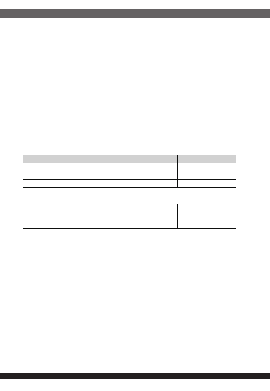
Table 7-3 – PSU SMB_Alert#
Item Description PMBus command MIN MAX
Talert_input
Timing from input voltage dropping to
0VAC to SMB_Alert
#
going low
STATUS_INPUT
UV Fault
4 msec
TOC_Warning
Timing from output over current
warning to SMB_Alert
#
going low
STATUS_IOUT 10 msec 20 msec
TOC_Warning_latch
Time the PSU holds the SMB_Alert
#
signal asserted after an over current
warning event
STATUS_IOUT 30sec
TOC_pmaxprotection Timing from output tripping
N
one 20μsec
Tover_temp Hot spot temp > warning threshold
STATUS_TEMPERATURE
Over temp warning
1 sec
Tsmbalert_shutdown
Minimum time PSU must continue to
operate within voltage regulation limits
and PWOK asserted after the
SMB_Alert
#
signal has been asserted
due to an over temperature event.
N
A 1sec
Tmax_warning
Hot spot temperature inside the PSU
that causes SMB_Alert
#
to assert.
MFR_TEMP2_MAX
Tmax_
continuous
Tshutdown
25
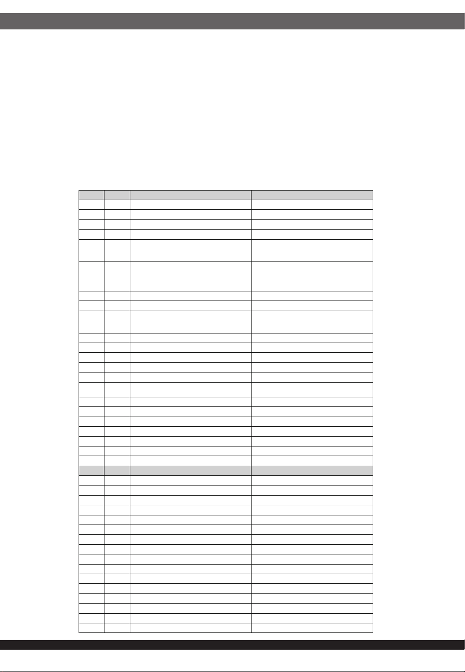
Table 7-4 – Voltage /Current / Power / Temperature /Fan Monitoring
6.1.9.SMB_Alert# operation in standby mode
The PSU shall assert the SMB_Alert# signal only when the main outputs are ON.
SMB_Alert# shall stay de-asserted when the PSU is in standby mode when any bits in the
STATUS commands get asserted.
6.2.Sensors
The following PMBus commands shall be supported for the purpose of monitoring current,
voltage, power, temperature and Fan speed. All sensors shall continue providing real time
data as long as the PMBus device is powered. This means in standby mode the main
output(s) of the PSU shall be zero amps and zero volts. Sensors shall meet requirements
from 100VAC to 120VAC and from 200VAC to 240VAC.
6.2.1.Accuracy requirements (Vin, Iin, Pin, Vout, Iout, Pout,Temp, Fan rpm)
The power supply shall follow PMBus commands for the purpose of monitoring current,
voltage, power, temperature and Fan state. All sensors shall continue providing real time
data as long as the PMBus device is powered. This means in standby mode the main
output(s) of the PSU shall be zero amps and zero volts. They shall be tested down to 5%
load.
Note : The power supply accuracy requirement must meet all the specified defined of input,
output and temperature range.
6.3.Black Box
The power supply shall save the latest PMBus data and other pertinent data into nonvola-
tile memory when a critical event shuts down the power supply. This data shall be
accessible via the SMBus interface with an external source providing power to the 12Vsb
pins. No AC power need to be applied to the power supply.
6.3.1.Data saving in Black Box
• General Fault
• Over voltage on output
• Over current on output
• Loss of AC input
• Input voltage fault
• Fan Failure
• Over temperature
Sensor < 20% load > 20% - 75% load > 75% - 100% Load
Input Voltage ± 3% ± 3% ± 3%
Input Current * ± 3% ± 3%
Input Power * ± 3% ± 3%
Temperature ± 5°C with Δ5%
FAN ± 10% from Spec.
Output Voltage ± 3% ± 3% ± 3%
Output Current * ± 3% ± 3%
Output Power * ± 3% ± 3%
26
6.4.In-System Firmware Upload
The Power supply shall have the capability to update its firmware via the PMBus
interface. This FW can be updated when in the system and in standby mode or
outside of the system with power applied to 12Vsb pins of power supply. The
primary and secondary sides have their own backup image in an external
EEPROM or internal FLASH. If the FW updated finally, the PSU could be able to
recover output with the backup version firmware.
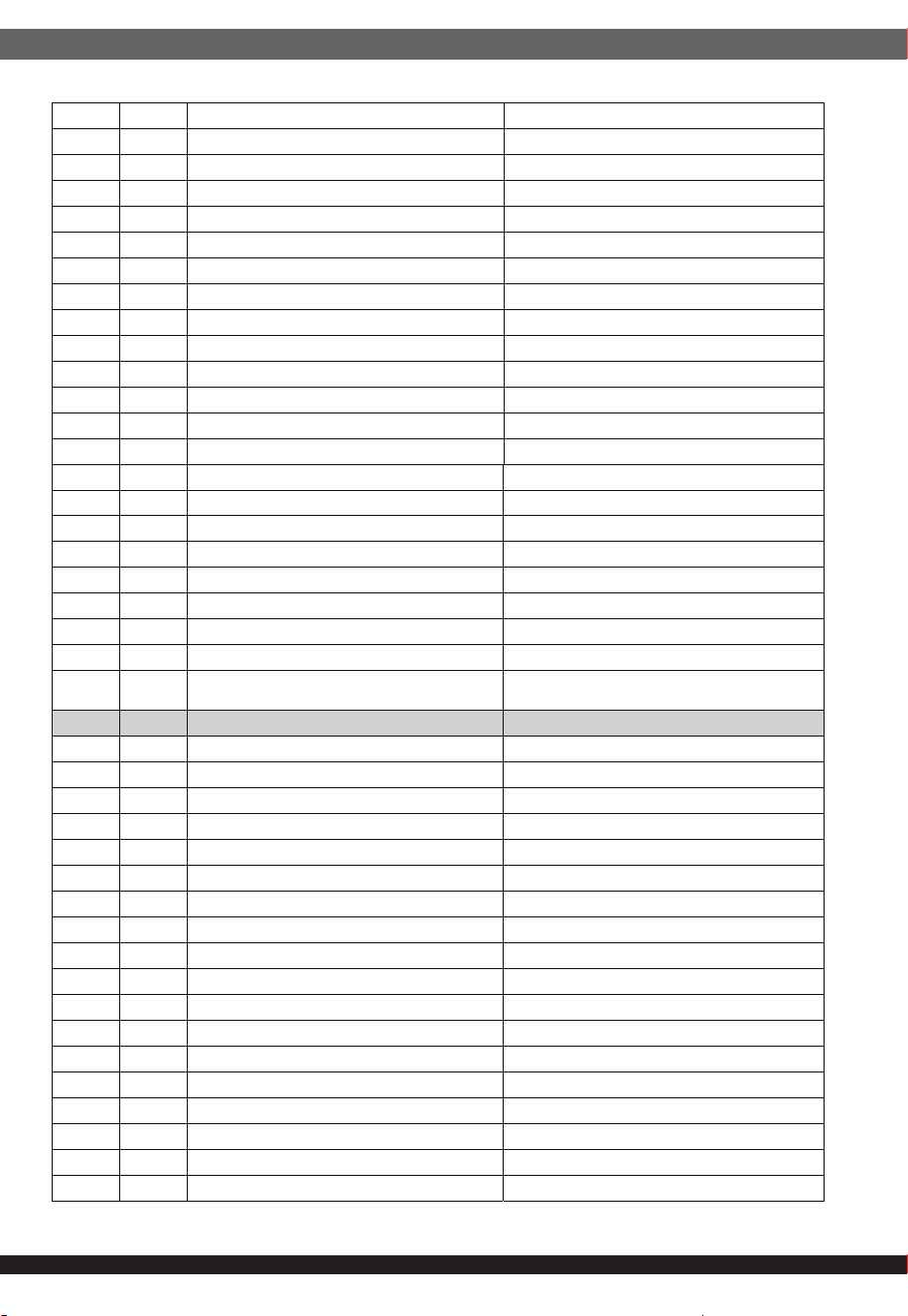
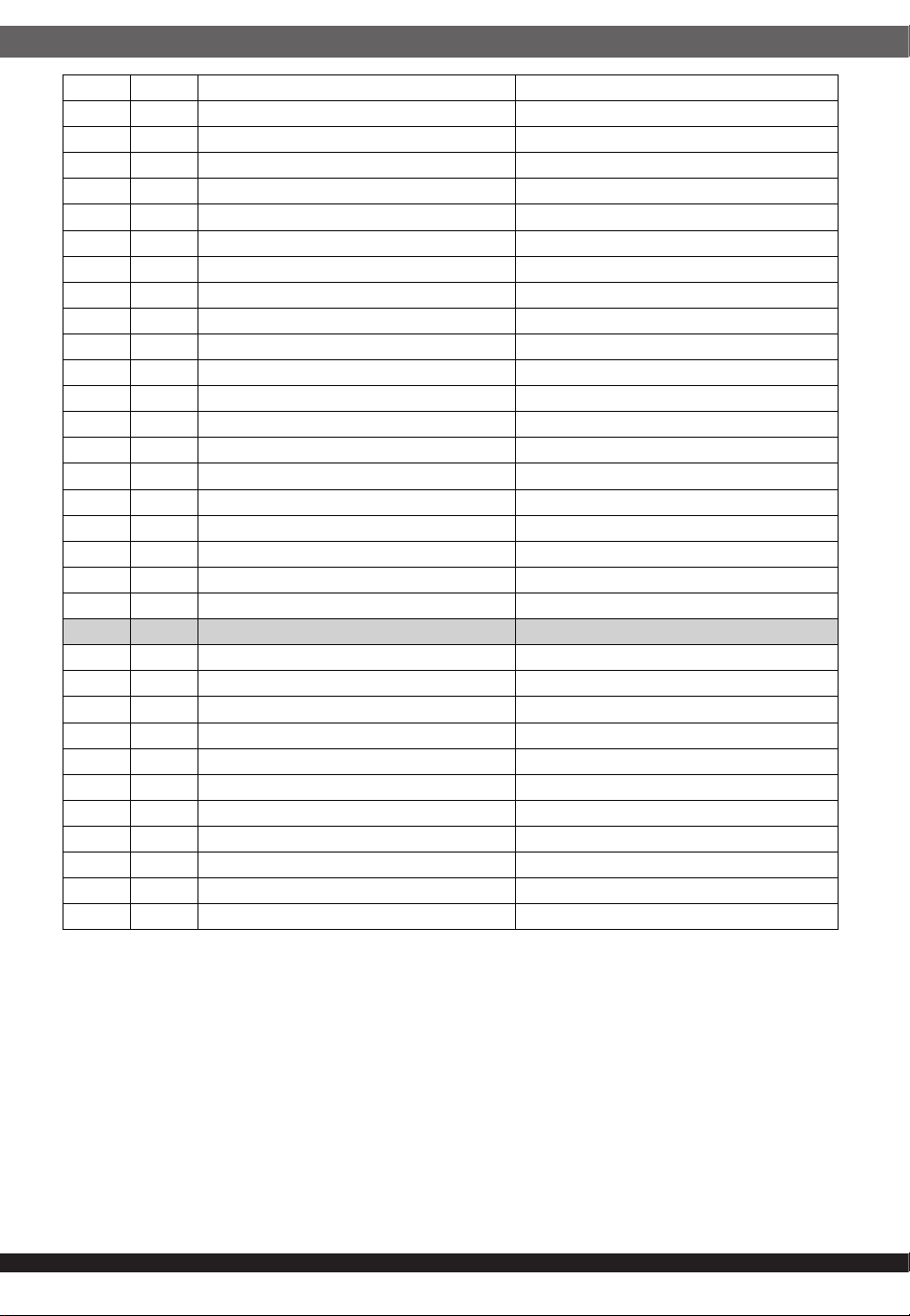
6.5.Supported PMBus Commands list
Table 7-5 – Supported PMBus
Code Pages Command SMBus Transaction Type Status bit mapping
00h NA PAGE Write Byte / Read Byte w/PEC
01h NA OPERATION Write Byte w/PEC
02h NA ON_OFF_CONFIG Write Byte w/PEC
03h NA CLEAR_FAULTS Send Byte w/PEC
05h NA
PAGE_PLUS_WRITE (used with
STATUS_WORD, STATUS_IOUT,
STATUS_INPUT, STATUS_TEMPERATURE)
Block Write w/PEC
Used with STATUS_INPUT,
STATUS_TEMPERATURE, STATUS_IOUT
06h NA
PAGE_PLUS_READ (used with
STATUS_WORD, STATUS_IOUT,
STATUS_INPUT, STATUS_TEMPERATURE)
Write Block Read Block Process Call w/PEC
Used with STATUS_INPUT,
STATUS_TEMPERATURE, STATUS_IOUT,
STATUS_WORD
19h
NA
CAPABILITY
Read Byte w/PEC
1Ah NA QUERY (used with any command) Block Write Block Read Process Call w/ PEC
1Bh NA
SMBALERT_MASK (used with
STATUS_INPUT, STATUS_TEMPERATURE,
STATUS_IOUT)
Reading: Write Block Read Block Process Call
w/PEC Writing: Write Word
20h NA VOUT_MODE Read Byte w/PEC
30h NA COEFFICIENT (used with READ_EIN) Block Write Block Read Process Call w/PEC
3Ah NA FAN_CONFIG_1_2
3Bh NA FAN_COMMAND_1
4Ah NA IOUT_OC_WARN_LIMIT Write Word / Read Word w/PEC
51h NA
OT_WARN_LIMIT (used to support testing
CLST)
Write word w/PEC
79h 00h, 23h STATUS_WORD Read Word w/PEC
(Low) 6 OFF PS off
4 IOUT_OC Indeterminate (Use STATUS_IOUT)
2 TEMPERATURE Indeterminate (Use STATUS_TEMPERATURE)
3 VIN_UV Indeterminate (Use STATUS_INPUT)
1 CML
Code Pages Command SMBus Transaction Type Status bit mapping
(High) 7 VOUT Failure
6 IOUT/POUT Indeterminate (Use STATUS_IOUT)
5 INPUT Indeterminate (Use STATUS_INPUT)
4 MFR_SPECIFIC (Incompatible Power Supply)
3 POWER_GOOD
#
2 FANS Indeterminate (Use STATUS_FANS)
7Ah NA STATUS_VOUT Read Byte w/PEC
7 VOUT_OV_FAULT Failure
4 VOUT_UV_FAULT Predictive failure
7Bh 00h, 23h STATUS_IOUT Read Byte w/PEC
7 Iout OC fault Failure
5 Iout OC warning Predictive failure
1 Pout OP fault Failure
0 Pout OP warning Predictive failure
7Ch 00h, 23h STATUS_INPUT Read Byte w/PEC
5 Vin UV warning Predictive failure
27
4 Vin UV fault AC Loss
3 Unit off for insufficient input AC Loss
1 Iin over current warning Predictive failure
0 Pin over power warning Predictive failure
7Dh 00h, 23h STATUS_TEMPERATURE Read Byte w/PEC
7 OT fault Fault
6 OT warning Predictive fault
7Eh 00h STATUS_CML
5 PEC Error Communication PEC Error
81h 00h STATUS_FANS_1_2 Read Byte w/PEC
7 Fan 1 fault Failure
6 Fan 2 fault Failure
5 Fan 1 warning Predictive failure
4 Fan 2 warning Predictive failure
86h NA READ_EIN Block Read w/ PEC
87h NA READ_EOUT Block Read w/ PEC
88h NA READ_VIN Read Word w/PEC
89h NA READ_IIN Read Word w/PEC
8Bh NA READ_VOUT Read Word w/PEC
8Ch NA READ_IOUT Read Word w/PEC
8Dh NA
READ_TEMPERATURE_1
(Ambient)
Read Word w/PEC
Code Pages Command SMBus Transaction Type Status bit mapping
8Eh NA READ_TEMPERATURE_2 (PFC Hot Spot) Read Word w/PEC
8Fh NA READ_TEMPERATURE_3 (SR Hot Spot) Read Word w/PEC
90h NA READ_FAN_SPEED_1 Read Word w/PEC
96h NA READ_POUT Read Word w/PEC
97h NA READ_PIN Read Word w/PEC
98h NA PMBUS_REVISION Read Byte w/PEC
99h NA MFR_ID Block Read w/ PEC
9Ah NA MFR_MODEL Block Read w/ PEC
9Bh NA MFR_REVISION Block Read w/ PEC
9Ch NA MFR_LOCATION Block Read w/ PEC
9Dh NA MFR_DATE Block Read w/ PEC
9Eh NA MFR_SERIAL Block Read w/ PEC
9Fh NA APP_PROFILE_SUPPORT Block Read w/ PEC
A0h NA MFR_VIN_MIN Read Word w/PEC
A1h NA MFR_VIN_MAX Read Word w/PEC
A2h NA MFR_IIN_MAX Read Word w/PEC
A3h NA MFR_PIN_MAX Read Word w/PEC
A4h 00h,23h MFR_VOUT_MIN Read Word w/PEC
28
7.FRU Requirements
7.1.FRU Data
The FRU Data format shall be compliant with the IPMI ver. 1.0 specification.
The following is the exact listing of the EEPROM content. During testing this
should be followed and verified.
7.2.FRU Device protocol
The FRU device will implement the same protocols as the commonly used
memorydevice, including Byte Read, Sequential Read, Byte Write and Page Read
protocols.
A5h 00h,23h MFR_VOUT_MAX Read Word w/PEC
A6h NA MFR_IOUT_MAX Read Word w/PEC
A7h NA MFR_POUT_MAX Read Word w/PEC
A8h NA MFR_TAMBIENT_MAX Read Word w/PEC
A9h NA MFR_TAMBIENT_MIN Read Word w/PEC
AAh NA MFR_EFFICIENCY_LL Block Read w/ PEC
ABh NA MFR_EFFICIENCY_HL Block Read w/ PEC
B1h NA PSU Internal Air Flow Read Byte w/PEC
B2h NA READ_TEMPERATURE_4 (Oring Hot Spot) Read Word w/PEC
C0h NA MFR_MAX_TEMP_1 Read Word w/PEC
C1h NA MFR_MAX_TEMP_2 Read Word w/PEC
C2h NA MFR_MAX_TEMP_3 Read Word w/PEC
C3h NA MFR_FAN_SPEED_MAX Read Word w/PEC
C4h NA MFR_FAN_SPEED_MIN Read Word w/PEC
C5h NA MFR_FW_ID1(ex: SECSR202AMP3A200A00) Block Read w/PEC
CCh
NA
Remote Control
Write Byte w/PEC
CDh NA Delay Time of Remote Control Write Byte w/PEC
D0h NA MFR_COLD_REDUNDANCY_CONFIG Read Byte w/PEC
D1h NA MFR_FW_ID Block Read w/PEC
D2h NA MFR_FW_REVISION Block Read w/PEC
D3h NA MFR_FW_DATE Block Read w/PEC
Code Pages Command SMBus Transaction Type Status bit mapping
D4h NA MFR_HW_COMPATIBILITY Block Read w/PEC
D5h NA MFR_FWUPLOAD_COMPATIBILITY Block Read w/PEC
D6h NA MFR_FWUPLOAD_MODE Read Byte w/PEC
D7h NA MFR_FWUPLOAD Block Write w/PEC
D8h NA MFR_FWUPLOAD_STATUS Block Read w/PEC
D9h NA MFR_FW_REVISION Block Read w/PEC
DCh NA MFR_BLACKBOX Block Read w/ PEC (154 byes)
DDh NA MFR_REAL_TIME_BLACK_BOX Block Write/Read w/ PEC (4 bytes)
DEh NA MFR_SYSTEM_BLACK_BOX Block Read w/ PEC (40 byes)
DFh NA MFR_BLACKBOX_CONFIG Read/Write Byte with PEC
E0h NA MFR_CLEAR_BLACKBOX Send Byte with PEC
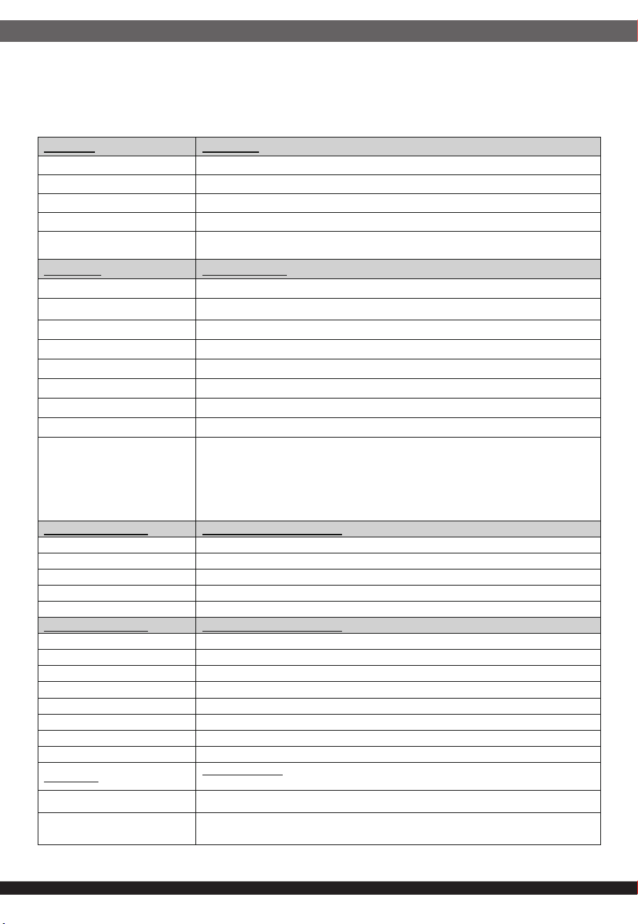
29
7.2.1.FRU Data Format
The information to be contained in the FRU device is shown in the following table 8-1.
Table 8-1 – FRU Data format
Area Type Description
Common Header As defined by the FRU document
Internal Use Area Not required, do not reserve
Chassis Info Area Not applicable, do not reserve
Board Info Area Not applicable, do not reserve
Product Info Area
As defined by the IPMI FRU document. Product information shall be defined as
follows:
Field Name Field Description
Manufacturer Name SilverStone
Product Name
SST-GM2000C-TFU
Product part/model number SST-CM2000GFTI-A
Product Version Defined based on the latest version of the model.
Product Serial Number {Defined at time of manufacture}
Asset Tag {Not used, code is zero length byte}
FRU File ID SEGSR202AMP3V100XXX
PAD Bytes {Added as necessary to allow for 8-byte offset to next area}
Multi-Record Area
As defined by the IPMI FRU document. The following record types shall be used on
this power supply:
- Power Supply Information (Record Type 0x00)
- DC Output (Record Type 0x01)
No other record types are required for the power supply.
Multi-Record information shall be defined as follows:
Field Name (PS Info) Field Information Definition
Overall Capacity (watts) 2000
Peak VA 2800
Inrush current (A) 40
Inrush interval (msec) 5
Low end input voltage range 1 90
Field Name (PS Info) Field Information Definition
High end input voltage range 1 132
Low end input voltage range 2 180
High end input voltage range 2 264
AC input dropout total. (msec) 6
Binary flags Set for: Hot Swap support.
Peak Wattage Set for: 2440Watts
Combined wattage None
Predictive fail tach support Supported
Field Name (Output)
Field Description: Two outputs are to be defined from #1 to #2, as follows: +1 .2.2V
and +12Vsb.
Output Information Set for: Standby on +12Vsb, No Standby on all others.
All other output fields Format per IPMI specification, using parameters in this specification.
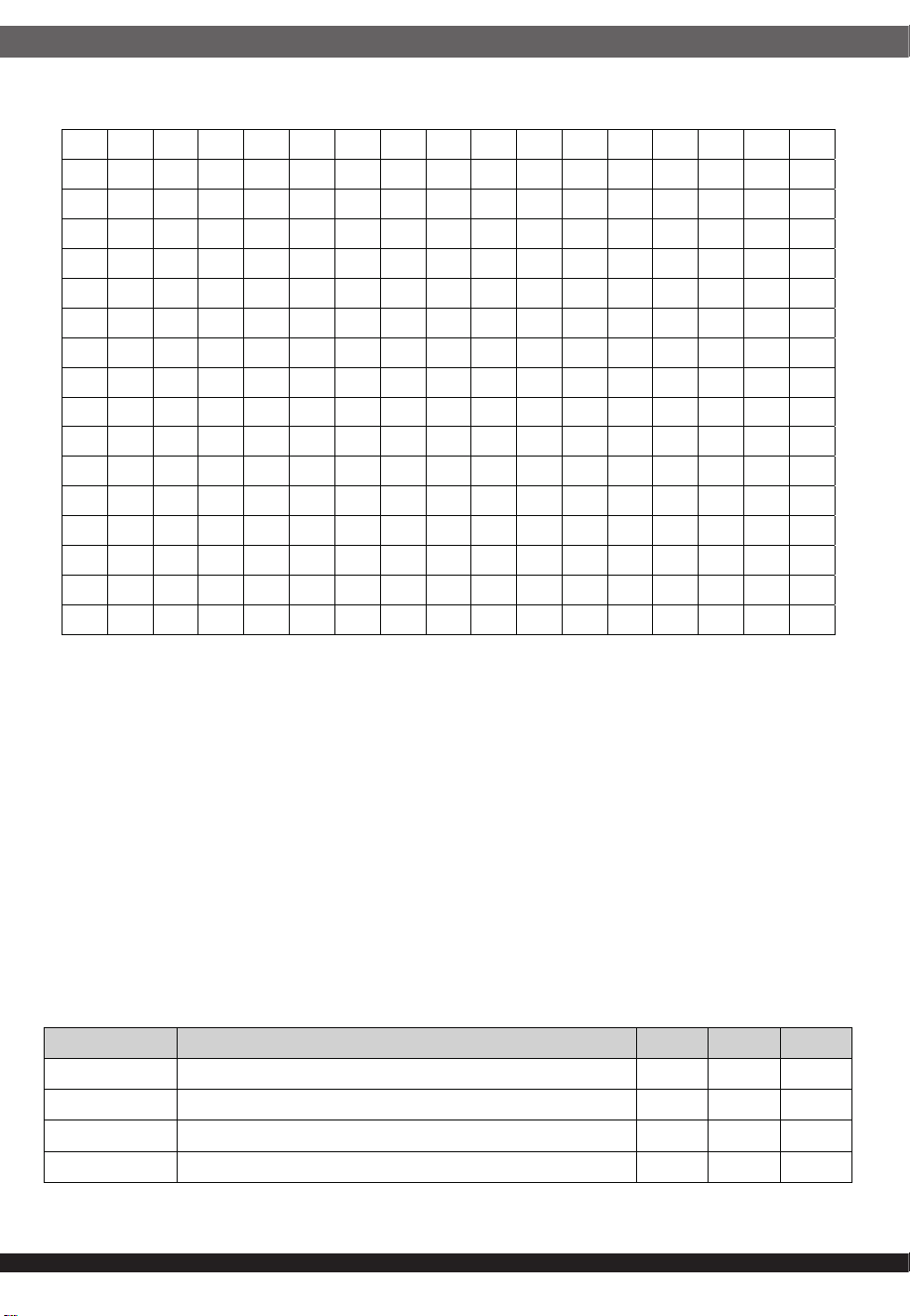
30
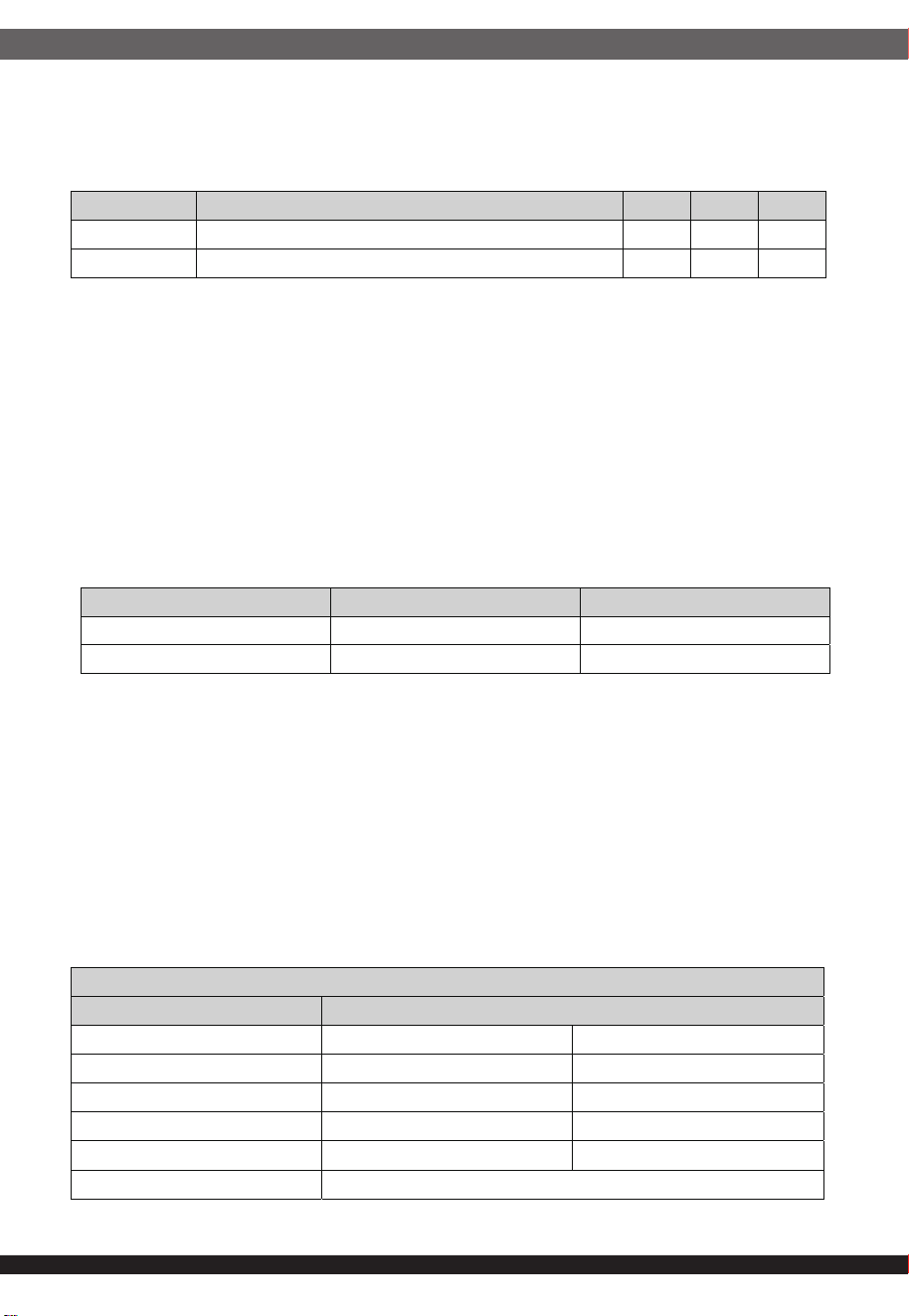
Table 8-2 – EEPROM Addressing (Example reference)
8.Environmental
The power supply shall operate normally, and sustain no damage as a result of
the environmental conditions listed in this chapter.
The defined operation condition includes temperature, humidity, altitude, shock
and vibration.
8.1.Temperature Requirements
The power supply shall operate within all specified limits over Top temperature
range. All airflow shall pass through the power supply and not over the exterior
surfaces of the power supply.
The power supply shall withstand thermal storage specified in Tnon-OP without
any damage.
Table 9-1 – Temperature Requirements
0x0 0x1 0x2 0x3 0x4 0x5 0x6 0x7 0x8 0x9 0xA 0xB 0xC 0xD 0xE 0xF
0x00
01 00 00 00 01 0D 00 F1 01 0C 19 C8 46 53 50 47
0x01
52 4F 55 50 CA 59 4E 45 45 30 37 35 30 42 4D D2
0x02
59 4E 45 45 30 37 35 30 42 4D 2D 32 52 30 31 50
0x03
31 30 C3 41 30 31 D3 46 37 35 31 30 41 54 39 30
0x04
34 30 30 56 30 35 30 30 30 31 3 15 09 01 D3 4E
0x05
45 45 53 52 37 35 31 41 4D 50 33 51 36 30 30 41
0x06
30 31 C1 00 00 00 00 A2 00 02 18 6B 7B EE 02 0
0x07
00 3C 00 28 23 20 67 0 0 0 0 2F 3F 0A 1F 00
0x08
00 00 00 00 00 01 02 0D 53 9D 01 B0 04 74 04 EC
0x09
04 78 00 00 00 24 F4 01 82 0D A9 C7 82 F4 01 DB
0xA0
01 0D 02 32 00 00 00 B8 0B FF FF FF FF FF FF FF
0xB0
FF FF FF FF FF FF FF FF FF FF FF FF FF FF FF FF
0xC0
FF FF FF FF FF FF FF FF FF FF FF FF FF FF FF FF
0xD0
FF FF FF FF FF FF FF FF FF FF FF FF FF FF FF FF
0xE0
FF FF FF FF FF FF FF FF FF FF FF FF FF FF FF FF
0xF0
FF FF FF FF FF FF FF FF FF FF FF FF FF FF FF FF
Item Description MIN MAX Unit
T
OP
Operating temperature range. -10 50 °C
ΔT Max temperature rise across power supply 15 °C
T
non-OP
Non-Operating temperature range. -40 70 °C
T
Δ_change
Rate of temperature change. 10 °C/hrs
31
8.2.Humidity
The power supply shall operate within all specified humidity Range defined in Table 9-2.
Note: 95% relative humidity is achieved with a dry bulb temperature of 50°C and a wet bulb
temperature of 54°C.
8.3.Altitude
The power supply shall operate within all specified limits over Aop Altitude range. The
change pressure condition shall not harm the power supply and the operation within
specified regulations shall be assured.
The power supply shall withstand Altitude storage specified in Anon-OP without any
damage.
8.4.Vibration
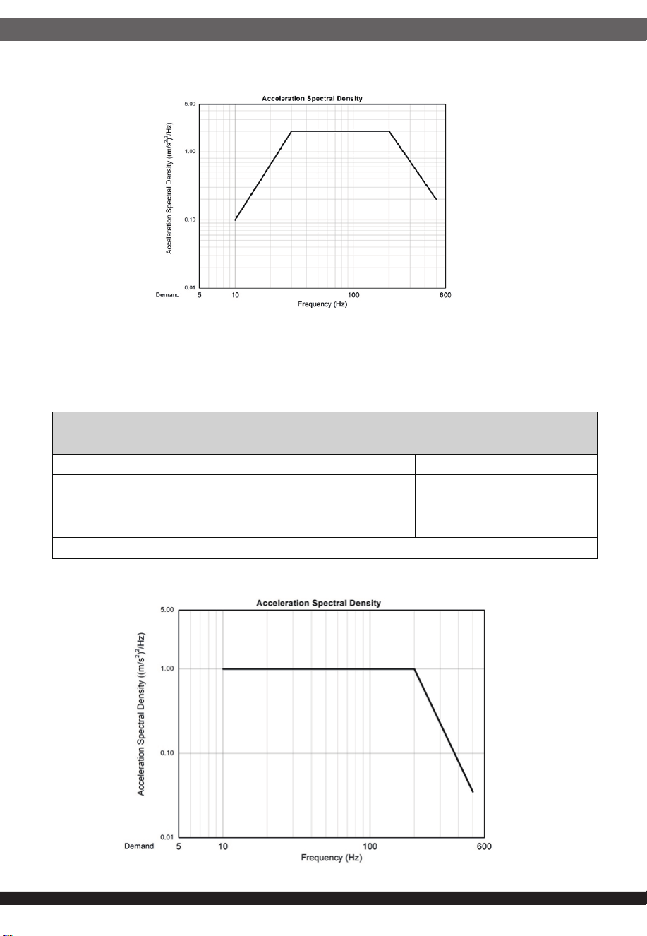
a)Operation(Random Vibration):
Each device shall be tested in three axes for a minimum of 30 minutes per axis. The device
shall be powered for the duration of the test at nominal input voltage and no load.
Table 9-2 – Humidity Requirements
Table 9-3 – Altitude Requirements
Table 9-4 – Operating Vibration
Item Description MIN MAX Unit
H
OP
Operating humidity range, non-condensing 5 85 %
H
non-OP
Non-Operating humidity range, non-condensing 5 95 %
Item Description Max.
AOP Operating Altitude range. 5,000m
Anon-
OP
Non-Operating Altitude range. 12,000m
Operating Vibration Profile Charts
Frequency Class II Acceleration Specification
Hz (m/s
2
)
2
/Hz G
2
/Hz
10 0.1 0.00046
30 2 0.0052
200 2 0.0052
500 0.2 0.0001
Grms=2.40
32
Figure 9-1 – Acceleration Spectral Density
Table 9-5 – Non-Operating Vibration Profile Charts
Figure 9-2 – Acceleration Spectral Density
b)Non-Operation(Random Vibration):
The products are in the shipping packaging shall be comply with non-operating
vibration testing for 3 resonant points with dwell 15min.
Non-Operating Vibration Profile Charts
Frequency Class II Acceleration Specification
Hz (m/s
2
)
2
/Hz G
2
/Hz
5 5 0.052
200 5 0.052
500 0.3 0.003
Grms=3.80

33
8.5.Thermal shock (Shipping)
The thermal shock -40°C to +65°C, non-operating, 10 cycles, transfer time shall not
exceed 5 minutes, duration of exposure to temperature extremes shall be 20 minutes.
8.6.Shock (Operating)
Each tested device shall be exposed to three shocks in each of three axes.
The amplitude of each shock shall be no less than 30g with a half sine wave shape and
duration of 11ms.
9.Regulatory Requirements
This product was evaluated as Information Technology Equipment (ITE), which may be
installed in offices, schools, computer rooms, and similar commercial type locations. The
suitability of this product for other product categories and environments (such as: medical,
industrial, telecommunications, NEBS, residential, alarm systems, test equipment, etc.)
other than ITE application, may require further evaluation.
9.1.Product Safety Compliance
a)UL/CUL (62368-1)
b)TUV(EN 62368-1)
c)CB (IEC 62368-1)
d)CE
e)FCC
9.2.Product EMC Compliance
The information contained in this section is the criteria and approvals of Power Supply
EMC requirements, The product is required to comply with RF EMISSIONS of EN
55032,CISPR 32 with minimum 6dB margin to Class A limit.
The power supply shall meet the following electrical EMS IMMUNITY requirements with EN
55035,CISPR 32 which defined in this section and Table 10-1,Table 10-2.
EN 61000-4-2 Electrostatic Discharges(ESD)
EN 61000-4-3 Radio Frequency Electromagnetic Field(RS)
EN 61000-4-4 Fast Transients Common Mode(EFT)
EN 61000-4-5 Surges
EN 61000-4-6 Radio Frequency Common Mode(CS)
EN 61000-4-8 Power Frequency Magnetic Field(PFMF)
EN 61000-4-11 Voltage Dips and Interruptions(DIP)
EN 61000-3-2 Harmonics Current Measurement
EN 61000-3-3 Voltage Fluctuations and Flicker Measurement
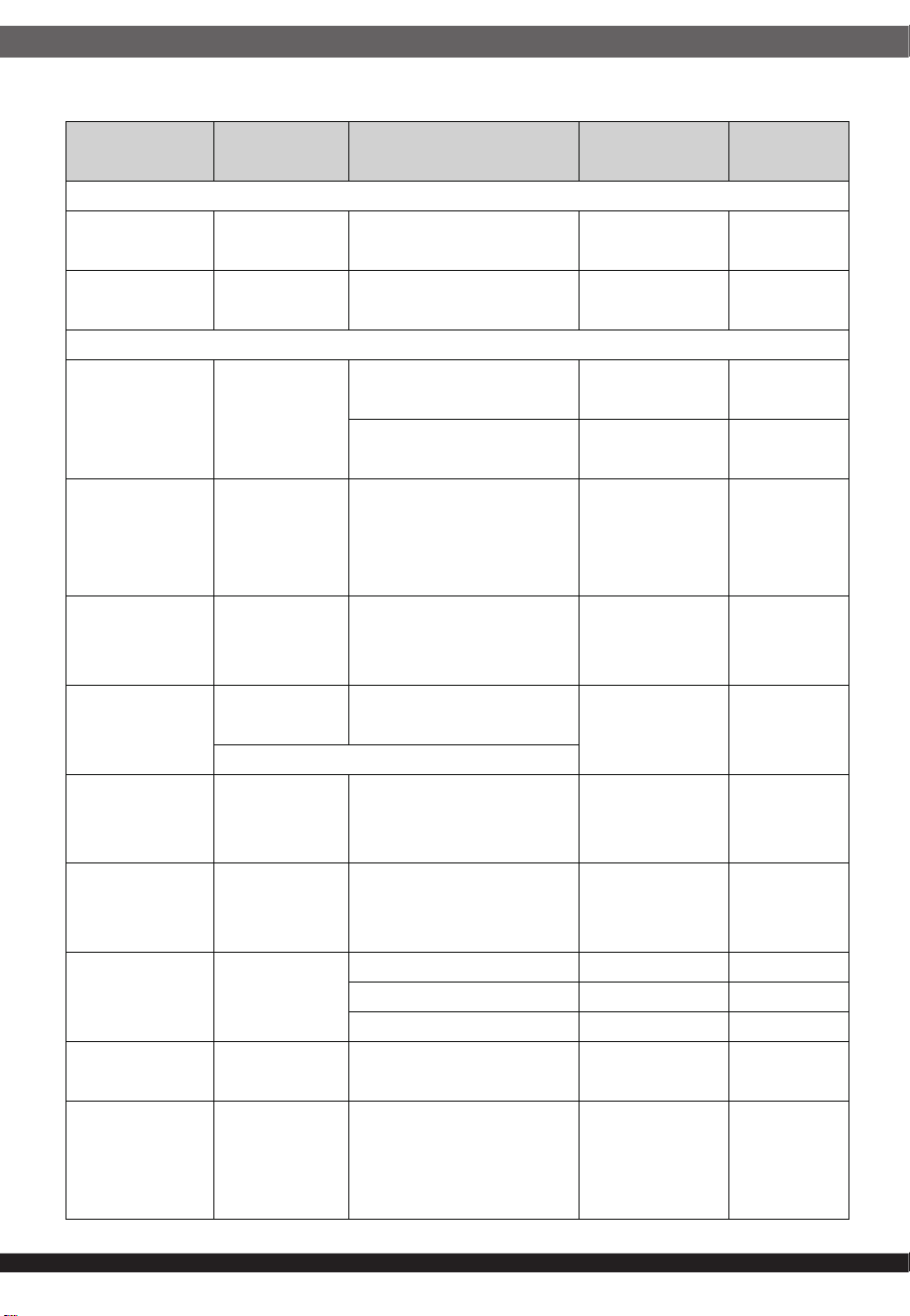
Table 10-1 – EMC Performance
Level Description
A The apparatus shall continue to operate as intended. No degradation of performance.
B The apparatus shall continue to operate as intended. No degradation of performance beyond spec limits.
C
Temporary loss of function is allowed provided the function is self-recoverable or can be restored by the
operation of the controls.
34
Table 10-2 – Product EMC Compliance
Category Standard Description Level / Limits
Performance
Criteria
EMISSIONS
Radiated Emissions EN 55032 30MHz – 1GHz Class A
Class A
6dB Margin
Conducted
Emissions
EN 55032 150KHz - 30MHz Class A
Class A
6dB Margin
IMMUNITY
Electrostatic
Discharges
(ESD)
EN 61000-4-2
Contact discharge
+/-8KV
Level 4 A
Air discharge
+/-15KV
Level 4 A
Radio Frequency
Electromagnetic
Field
(RS)
EN 61000-4-3 3V/m Level 2 A
Fast Transients
Common Mode
(EFT)
EN 61000-4-4 +/- 2 kV A
Surges
EN 61000-4-5
CM±2KV (12 ohm)
DM±1KV (2 ohm)
Level 3 A
Radio Frequency
Common Mode
(CS)
EN 61000-4-6 3Vrms Level 2 A
Power Frequency
Magnetic Field
(PFMF)
EN 61000-4-8 1A/m Level 1 A
Voltage Dips and
Interruptions
(DIP)
EN 61000-4-11
Voltage Residual(%) : <5 0.5 cycle B
Voltage Residual(%) : 70 25 cycle B
Voltage Residual(%) : <5 250 cycle B
Harmonics Current
Measurement
EN 61000-3-2 AC supply <16Amps per phase Refer to standard
Voltage
Fluctuations and
Flicker
Measurement
EN 61000-3-3 AC supply <16Amps per phase Refer to standard
35
9.3.Hi-Pot
The power supply module shall comply with the minimum production Hi-Pot (High Poten-
tial)Test at 1800Vac/ 3Seconds with a trigger of 15mA current. The test shall be applied
between Primary (AC Line and Neutral) and Earth Ground (Chassis/Input Receptacle
ground terminal).
9.4.Mean Time between Failures (MTBF)
The power supply shall have a minimum MTBF at continuous operation of 200,000 hours
calculated at 100%, according to Telcordia SR-332 Issue 3 at 25°C excluding the Fan
MTBF, and at least 100,000 hours including the fan MTBF.
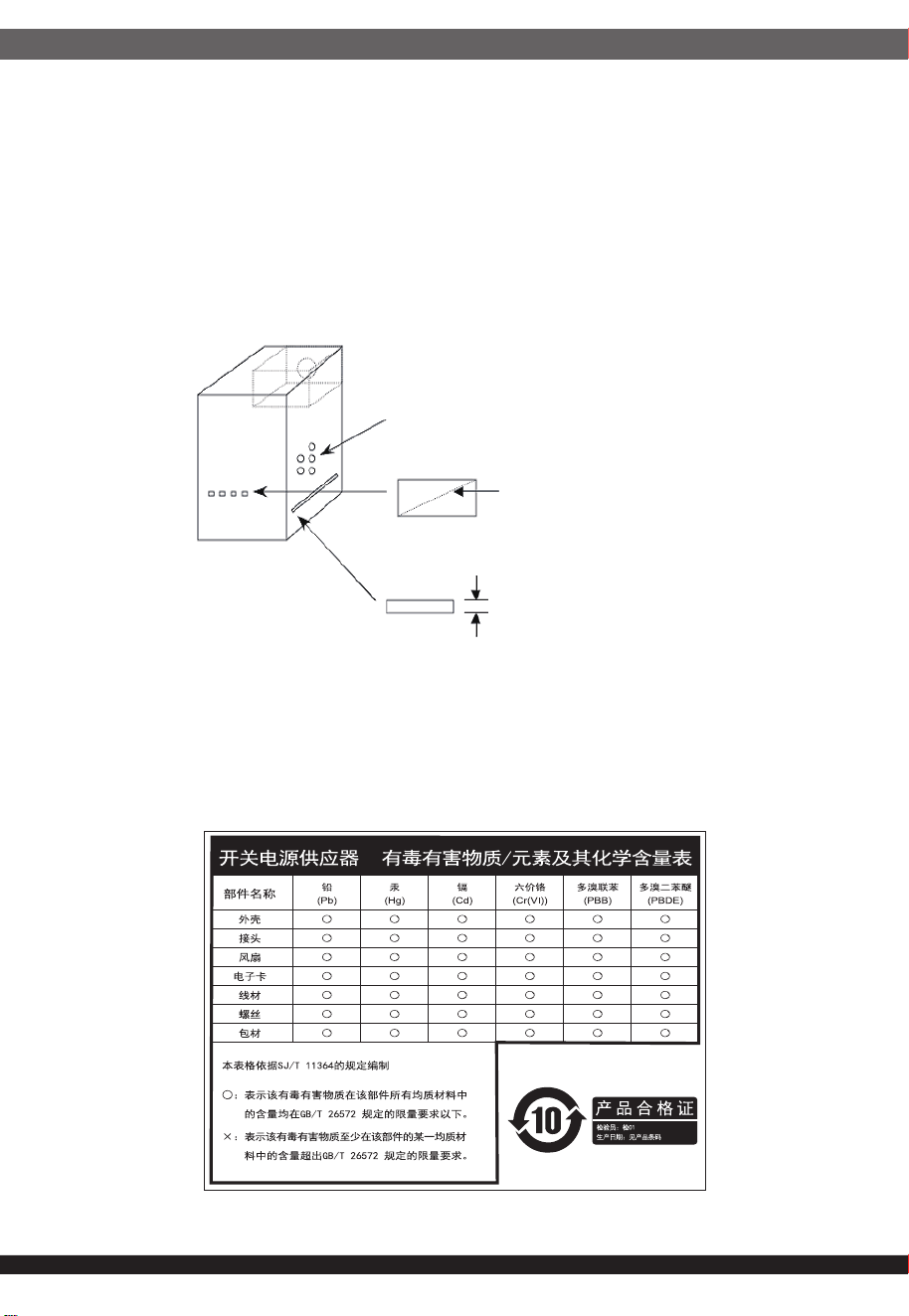
ⳈᕥϡᮐPP
ᇡ㾦㎮ϡᮐPP
ᇀᑺᇣᮐPPࠛ䭋ᑺϡ䰤
Openings that do not exceed 1mm in width regardless of length
Openings that do not exceed 5mm in any dimension
ᴀ⫶ક䔌ߎ᳝䱾㛑䞣ˈ⚎䙓ܡ᪡ᰖⱐ⫳䱾ˈ䷜ᮐ㺱ܹ㋏㍅″←Ϻᇛ᠔᳝䀁٭ᅝ㺱ཹ⭊ᕠᠡৃ䭟ଳ䳏⑤DŽ
ᴀ⫶કП䳏⑤䔌ߎ䴲ቀ䳏䰤ࠊൟ䳏⑤ˈ䂟䗷Փ⫼䰆☿←П䙞ˈҹ䙓ܡ☿♑䱾ⱐ⫳DŽ
%60,52+6䊛㿞
KWWSZZZVLOYHUVWRQHWHNFRPGRZQORDGV36856'SGI

36
This device complies with Part 15 of the FCC Rules.
Operation is subject to the following two conditions:
(1) this device may not cause harmful interference, and
(2) this device must accept any interference received,
including interference that may cause undesired operation.
Please refer to SilverStone website for latest specifications updates.
The equipment a Class | Switching Power Supply intended to use
for information technology equipment or Audio and Video equipment.
※付属の電源コードは当該製品専用です。他の機器に使用しないでください。
Model (safety certification): SST-CM2000GFTI-A
SST-CM2400GFTI-A
本製品は2000W;2400Wの出力が可能な高出力電源となります。
・一般家庭のコンセント(1500W)の場合は、1300W未満の消費電力でご利用ください。
・日本国内向けに販売されている本製品の付属電源ケーブルは100V(最大15A)専用となります。
・本製品に200V用電源ケーブル、および100V/20A用電源ケーブルの同梱はございません。
・100V/15A以外の環境でご利用の際は、安全の為、必要な電源ケーブルを別途ご用意ください。