MeiGProductManualofSLM750Module
SLM750ModuleHardwareDesign Page 1, total 84 pages
MeiG Product
Manual of SLM750
VersionNumber:V1.1
Company:MeiGSmartTechnologyCo.,Ltd
ReleasedDate:2018/8/13

MeiGProductManualofSLM750Module
SLM750ModuleHardwareDesign Page 2, total 84 pages
IMPORTANTNOTICE
COPYRIGHTNOTICE
Copyright©MeiGSmartTechnologyCo.,Ltd.Allrightsreserved.
AllcontentsofthismanualareexclusivelyownedbyMeiGSmar t TechnologyCo.,Ltd(MeiGSmartforshort),
whichisundertheprotectionofChineselawsandcopyrightlawsininternationalconventions.Anyoneshall
not copy, spread, distribute, modify or use in
other ways with its contents without the written
authorization of MeiG Smart. Those who violated will be investigated by corresponding legal liability in
accordancewiththelaw.
NOGUARANTEE
MeiG Smart makes no representation or warranty, either express or implied, for any content in this
document, andwill not be
liable for any specific merchantability andapplicable or any indirect,particular
andcollateraldamage.
CONFIDENTIALITY
Allinformationcontainedhere(includinganyattachments)isconfidential.Therecipientacknowledgesthe
confidentialityofthisdocument,andexceptforthespecificpurpose,thisdocumentshallnotbedisclosed
toanythirdparty.
DISCLAIMER
MeiG Smart will
not take any responsibility for any property and health dam agecaused by the abnormal
operationofcustomers.Pleasedevelopthe productaccordingtothetechnicalspecificationanddesigning
referenceguidewhichdefinedintheproductmanual.MeiGSmarthavetherighttomodify thedocument
accordingtotechnicalrequirementwith
noannouncementtothecustomer.

MeiGProductManualofSLM750Module
SLM750ModuleHardwareDesign Page 3, total 84 pages
Revising History
Table 1: Revising records
REVISION DATE DESCRIPTION
V1.0 2018‐04‐01 Initial
V1.1
2018‐12‐14
Modifypowerconsumption,RF,packaging

MeiGProductManualofSLM750Module
SLM750ModuleHardwareDesign Page 4, total 84 pages
Contents
1 Introduction ............................................................................................................................................................ 8
1.1 Safety Information ....................................................................................................................................... 9
1.1 Safety Information ....................................................................................................................................... 9
1.2 Purpose ...................................................................................................................................................... 10
1.3 Content list ................................................................................................................................................. 10
2 Product Overview ..................................................................................................................................................11
2.1 Basic Description ........................................................................................................................................11
2.2 Main performance .......................................................................................................................................11
2.3 Functional diagram .................................................................................................................................... 14
2.4 Evaluation Board ....................................................................................................................................... 15
3 Application Interface ............................................................................................................................................ 16
3.1 General Description ................................................................................................................................... 16
3.2 LCC Card Interface Definition .................................................................................................................. 17
3.3 Pin Description .......................................................................................................................................... 17
3.4 Operating Mode ......................................................................................................................................... 28
3.5 Power Saving ............................................................................................................................................. 30
3.5.1 Sleep Mode ..................................................................................................................................... 30
3.5.1.1 USB Application (with USB remote waking-up function) .................................................. 30
3.5.1.2 USB Application (without USB Suspend function) ............................................................. 31
3.5.1.3 Hardware I/O control sleep mode ........................................................................................ 31
3.5.2 Flight Mode .................................................................................................................................... 32
3.5.2.1 Hardware I/O interface controls flight mode ....................................................................... 32
3.5.2.2 AT command controls flight mode ....................................................................................... 32
3.6 Power Supply ............................................................................................................................................. 32
3.6.1 Power supply pins ........................................................................................................................... 32
3.6.2 Decrease voltage drop ..................................................................................................................... 33
3.6.3 Reference design for power supply ................................................................................................ 34
3.6.4 VDD_EXT voltage output .............................................................................................................. 35
3.7 Turn On and Off ......................................................................................................................................... 35
3.7.1 Turn on module using the PWRKEY.............................................................................................. 35
3.7.2 Turn off module using the PWRKEY pin ....................................................................................... 37
3.7.2.1 PWRKEY pin shutdown ...................................................................................................... 37
3.7.2.2 AT command shutdown ........................................................................................................ 38
3.8 Reset the Module ....................................................................................................................................... 38
3.8.1 Hardware reset ................................................................................................................................ 39
3.8.2 AT command reset .......................................................................................................................... 40
3.9 USIM/SIM Card Interface ......................................................................................................................... 40
3.10 USB Interface .......................................................................................................................................... 42
3.10.1 USB pin description ...................................................................................................................... 43
3.10.2 USB reference circuit .................................................................................................................... 43
3.10.3 USB driver .................................................................................................................................... 44
3.11 UART Interface ........................................................................................................................................ 44
3.12 PCM and I2C Interface ............................................................................................................................ 46

MeiGProductManualofSLM750Module
SLM750ModuleHardwareDesign Page 5, total 84 pages
3.13 Network Status Indication ....................................................................................................................... 48
3.14 Status ....................................................................................................................................................... 49
3.15 ADC Function .......................................................................................................................................... 50
3.16 SGMII Interface ....................................................................................................................................... 50
3.17 Wireless Connectivity Interfaces ............................................................................................................. 52
3.17.1 WLAN Interface ........................................................................................................................... 54
3.17.2 BT Interface .................................................................................................................................. 55
3.18 SD Card Interface .................................................................................................................................... 55
3.19 USB_BOOT Interface .............................................................................................................................. 57
4 GNSS .................................................................................................................................................................... 58
4.1 General Description ................................................................................................................................... 58
4.2 GNSS Performance .................................................................................................................................... 58
4.3 Layout Guideline ....................................................................................................................................... 59
5 Antenna Interface .................................................................................................................................................. 59
5.1 Antenna Interface ....................................................................................................................................... 59
5.2 RF Reference Circuit ................................................................................................................................. 60
5.3 Antenna Installation ................................................................................................................................... 62
5.3.1 Antenna requirements ..................................................................................................................... 62
5.3.2 RF output power ............................................................................................................................. 62
5.3.3 RF receiving sensitivity .................................................................................................................. 63
5.3.4 Operating frequency ....................................................................................................................... 64
5.3.5 Antenna requirements ..................................................................................................................... 64
6 Electrical characteristics ....................................................................................................................................... 65
6.1 Limit voltage range .................................................................................................................................... 65
6.2 Temperature range ..................................................................................................................................... 66
6.3 Electrical Characteristics of Interface Operation Status ............................................................................ 66
6.4 Module Power Consumption Range .......................................................................................................... 67
6.5 Environmental Reliability Requirements ................................................................................................... 72
6.6 ESD Characteristics ................................................................................................................................... 73
7 Mechanical Dimensions........................................................................................................................................ 74
7.1 Mechanical Dimensions of the Module ..................................................................................................... 74
7.2 Recommended Packaging .......................................................................................................................... 76
7.3 Top View of the Module ............................................................................................................................ 77
7.4 Bottom View of the Module ...................................................................................................................... 77
8 Storage and Manufacturing ................................................................................................................................... 78
8.1 Storage ....................................................................................................................................................... 78
8.2 Manufacturing and Welding ...................................................................................................................... 79
8.3 Packing ...................................................................................................................................................... 79
9 Appendix A References......................................................................................................................................... 81
9.1 Related Documents .................................................................................................................................... 81
9.2 Terms and Abbreviations ........................................................................................................................... 81
10 Appendix B GPRS Coding Scheme .................................................................................................................... 83

MeiGProductManualofSLM750Module
SLM750ModuleHardwareDesign Page 6, total 84 pages
Table
TABLE 1: REVISING RECORDS....................................................................................................................................3
T
ABLE 2: SUPPORTED BAND OF SLM750V..............................................................................................................11
T
ABLE 3: LIST OF MAIN FEATURES OF THE MODULE.................................................................................................12
T
ABLE 4: IO PARAMETERS DEFINITION....................................................................................................................17
T
ABLE 5: PIN DESCRIPTION......................................................................................................................................18
T
ABLE 6: OVERVIEW OF OPERATING MODES...........................................................................................................28
T
ABLE 7: RELATED POWER SUPPLY INTERFACES.......................................................................................................33
T
ABLE 8: RESET_N PIN DESCRIPTION.....................................................................................................................39
T
ABLE 9: USIM/SIM CARD INTERFACE DESCRIPTION..............................................................................................40
T
ABLE 10: USB INTERFACE DESCRIPTION................................................................................................................43
T
ABLE 11: MAIN UART PIN DESCRIPTION................................................................................................................45
T
ABLE 12: DEBUG UART PIN DESCRIPTION.............................................................................................................45
T
ABLE 13: UART LOGICAL LEVEL...........................................................................................................................45
T
ABLE 14: PIN DESCRIPTION FOR PCM INTERFACE..................................................................................................48
T
ABLE 15: PIN DEFINITION OF NETWORK INDICATOR..............................................................................................48
T
ABLE 16: WORKING STATE OF THE NETWORK INDICATOR.....................................................................................49
T
ABLE 17: STATUS PIN DESCRIPTION.....................................................................................................................49
T
ABLE 18: ADC PIN DESCRIPTION............................................................................................................................50
T
ABLE 19: PIN DEFINITION OF SGMII INTERFACE....................................................................................................50
T
ABLE 20: PIN DEFINITION OF WIRELESS CONNECTIVITY INTERFACES...................................................................52
T
ABLE 21: PIN DEFINITION OF THE SD CARD INTERFACE........................................................................................55
T
ABLE 22: PIN DEFINITION OF USB_BOOT INTERFACE..........................................................................................57
T
ABLE 23: GNSS PERFORMANCE.............................................................................................................................58
T
ABLE 24: RF ANTENNA PIN DEFINITION..................................................................................................................59
T
ABLE 25: ANTENNA REQUIREMENTS......................................................................................................................62
T
ABLE 26: RF OUTPUT POWER.................................................................................................................................63
T
ABLE 27: RF RECEIVING SENSITIVITY....................................................................................................................63
T
ABLE 28: OPERATING FREQUENCY.........................................................................................................................64
T
ABLE 29: ANTENNA REQUIREMENTS......................................................................................................................64
T
ABLE 30: DIVERSITY ANTENNA REQUIREMENTS.....................................................................................................65
T
ABLE 31: LIMIT VOLTAGE RANGE...........................................................................................................................65
T
ABLE 32: TEMPERATURE RANGE............................................................................................................................66
T
ABLE 33: LOGICAL LEVEL OF NORMAL DIGITAL IO SIGNAL....................................................................................66
T
ABLE 34: ELECTRICAL CHARACTERISTICS IN POWER SUPPLY STATUS.....................................................................67
T
ABLE 35: CONSUMPTION........................................................................................................................................67
T
ABLE 36: ENVIRONMENTAL RELIABILITY REQUIREMENTS.....................................................................................72
T
ABLE 37: ESD PERFORMANCE PARAMETERS (TEMPERATURE: 25℃, HUMIDITY: 45%)..........................................73
T
ABLE 38: TERMS AND ABBREVIATIONS...................................................................................................................81
T
ABLE 39: DESCRIPTION OF CODING SCHEMES........................................................................................................83

MeiGProductManualofSLM750Module
SLM750ModuleHardwareDesign Page 7, total 84 pages
Figure
FIGURE 1 FUNCTIONAL DIAGRAM............................................................................................................................15
F
IGURE 2 PIN ASSIGNMENT......................................................................................................................................17
F
IGURE 3 SLEEP MODE APPLICATION WITH USB REMOTE WAKING-UP FUNCTION....................................................31
F
IGURE 4 POWER REQUIREMENTS FOR BURST TRANSMISSION.................................................................................34
F
IGURE 5 STAR STRUCTURE OF POWER SUPPLY........................................................................................................34
F
IGURE 6 DC POWER SUPPLY CIRCUIT......................................................................................................................35
F
IGURE 7 TURN ON THE MODULE USING DRIVING CIRCUIT......................................................................................36
F
IGURE 8 TURN ON THE MODULE USING KEYSTROKE...............................................................................................36
F
IGURE 9 TIMING OF TURNING ON MODULE.............................................................................................................37
F
IGURE 10 TIMING OF TURNING OFF MODULE..........................................................................................................38
F
IGURE 11 REFERENCE CIRCUIT OF RESET_N BY USING DRIVING CIRCUIT............................................................39
F
IGURE 12 REFERENCE CIRCUIT OF RESET_N BY USING BUTTON..........................................................................39
F
IGURE 13RESET TIMING OF RESET_N...................................................................................................................40
F
IGURE 14 REFERENCE CIRCUIT FOR 8-PIN USIM/SIM CONNECTOR.......................................................................41
F
IGURE 15 REFERENCE CIRCUIT FOR 6-PIN USIM/SIM CONNECTOR.......................................................................41
F
IGURE 16 USB REFERENCE CIRCUIT.......................................................................................................................43
F
IGURE 17 REFERENCE CIRCUIT OF LEVEL CONVERSION CHIP.................................................................................46
F
IGURE 18 TIMING IN SHORT FRAME MODE..............................................................................................................47
F
IGURE 19 TIMING IN LONG FRAME MODE...............................................................................................................47
F
IGURE 20 REFERENCE DESIGN FOR PCM CIRCUIT..................................................................................................48
F
IGURE 21 REFERENCE CIRCUIT OF STATUS...........................................................................................................50
F
IGURE 22 SIMPLIFIED BLOCK DIAGRAM FOR ETHERNET APPLICATION.................................................................51
F
IGURE 23 REFERENCE CIRCUIT OF SGMII INTERFACE WITH PHY AR8033 APPLICATION.....................................52
F
IGURE 24 REFERENCE CIRCUIT OF WIRELESS CONNECTIVITY INTERFACES WITH SLM158...................................54
F
IGURE 25 REFERENCE CIRCUIT OF SD CARD APPLICATION...................................................................................56
F
IGURE 26 CIRCUIT OF USB_ROOT INTERFACE.....................................................................................................58
F
IGURE 27 RF REFERENCE CIRCUIT..........................................................................................................................61
F
IGURE 28 GNSS ANTENNA REFERENCE CIRCUIT....................................................................................................61
F
IGURE 29 MODULE TOP AND SIDE DIMENSION (UNIT: MM).....................................................................................74
F
IGURE 30 MODULE BOTTOM DIMENSIONS (UNIT: MM)...........................................................................................75
F
IGURE 31 TOP VIEW OF RECOMMENDED PACKAGING (UNIT: MM)...........................................................................76
F
IGURE 32 TOP VIEW OF THE MODULE......................................................................................................................77
F
IGURE 33 BOTTOM VIEW OF THE MODULE..............................................................................................................77
F
IGURE 34 REFLOW SOLDERING TEMPERATURE PROFILE.........................................................................................79
F
IGURE 35 PALLET PACKAGING(UNIT: MM)..............................................................................................................80

MeiGProductManualofSLM750Module
SLM750ModuleHardwareDesign Page 8, total 84 pages
1 Introduction
This document defines SLM750 modules and describes its air interface and hardware interface
which are connected with your application.
The document can help you quickly understand SLM750 interface specifications, electrical and
mechanical details and other related product information. Associated with application notes and
user guide, you can apply SLM750 in wireless applications easily.
SLM750 wireless module is a broadband wireless vehicle-mounted product used for various
network standards like TD-LTE/FDD LTE/WCDMA/TD-SCDMA/EVDO/CDMA/GSM.
Supported access rate of SLM750:
TD-LTE: 130Mbps/35Mbps
FDD LTE: 150Mbps/50Mbps
WCDMA reaches DC HSPA+: 42Mbps/5.76Mbps
EVDO reaches EVDO RevA: 3.1Mbps/1.8Mbps
TD-SCDMA reaches HSPA: 4.2Mbps/2.2Mbps
CDMA1x: 153.6kbps/153.6kbps
GSM reaches EDGE: 236.8kbps/236.8kbps
SLM750 provides high-speed broadband data access. In addition, it provides voice, SMS,
address book, GPS/Beidou and other functions, which can be used in mobile broadband access,
video surveillance, security, vehicle equipment and other products.
MeiGProductManualofSLM750Module
SLM750ModuleHardwareDesign Page 9, total 84 pages
1.1 Safety Information
Observing the following safety information can keep you safe and protect the product and its
working environment from potential damage.
Full attention must be given to driving at all times in order to reduce the risk
of an accident. Using a mobile while driving (even with a handsfree kit)
causes distraction and can lead to an accident. Stop the car before you make a
call.
Switch off the mobile terminal devices before boarding an aircraft. The
operation of wireless appliances in an aircraft is forbidden, so as to prevent
interference with communication systems. Ignore the note will threaten flight
safety or even break the law.
Pay attention to restrictions on the use of mobile terminal device in hospitals
or health care facilities. RF interference can cause medical equipment to run
out of order, so it is necessary to turn off the mobile terminal devices.
Mobile terminal device cannot be guaranteed to connect in all conditions, for
example no mobile fee or with an invalid SIM card. While you are in this
condition and need emergent help, remember to use emergency call. The
mobile terminal device must be switched on and in a service area with
adequate signal strength in order to make or receive a call.
Your mobile terminal device receives and transmits radio frequency signal
when it is on. RF interference can occur if it is use to close to TV set, radio,
computer or other electronic equipment.
Please keep the mobile device away from areas with potentially explosive
atmospheres. When you are near a gas station, oil depot, chemical plant or an
explosion site, please turn off your mobile terminal. There is a potential safety
hazard to operate electronic equipment at any potential explosion hazardous
locations.

MeiGProductManualofSLM750Module
SLM750ModuleHardwareDesign Page 10, total 84 pages
1.2 Purpose
This document describes basic functions and main features of SLM750 wireless module, as
well as hardware interface and its application, features of structure and electronics, and power index,
in order to guide you to embed SLM750 in various application terminals.
1.3 Content list
The document includes:
Chapter 1 introduces safety information, purpose of the document and revised records;
Chapter 2 describes basic functions and main features of SLM750 wireless module;
Chapter 3 describes functions, features, and applications of each hardware interface of
SLM750;
Chapter 4 describes related features of GNSS;
Chapter 5 introduces related information and notes of antenna interface;
Chapter 6 describes electronic features of SLM750;
Chapter 7 describes structure features and notes of SLM750;
Chapter 8 describes storage and production notes of SLM750;
Chapter 9 Appendix A: Reference documents and abbreviations;
Chapter 10 Appendix B: GPRS encoding scheme
MeiGProductManualofSLM750Module
SLM750ModuleHardwareDesign Page 11, total 84 pages
2 Product Overview
2.1 Basic Description
SLM750 is a wireless communication module of TD-LTE/FDD LTE/TD-SCDMA/WCDMA/
EVDO/CDMA/GSM with diversity receiving function. It supports TD-LTE and FDD LTE, and
downwards compatible with DC-HSPA+ of WCDMA, TD-HSPA of TD-SCDMA, network data
connection of EVDO RevB, which provides functions of voice, analog voice, SMS, and
communication for your applications. The module has 3 sub-modes: SLM750VC, SLM750VE,
SLM750VA. The following table shows the supported bands of the module.
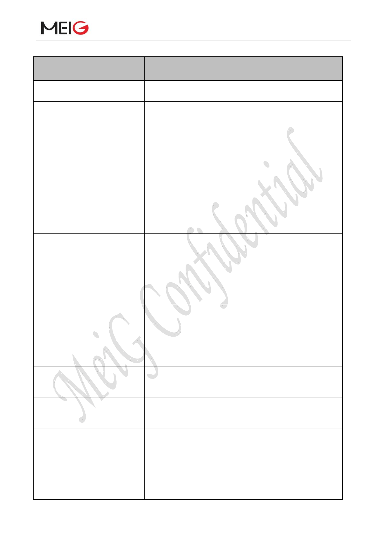
Table 2: Supported band of SLM750
Network SLM750VC SLM750VE SLM750VA
TD-LTE B38/B39/B40/B41 B40 B41
FDD LTE B1/B3/B5/B8 B1/B3/B5/B7/B8/B20 B2/B4/B5/B12/B13/B17/B25/B26
WCDMA B1/B8 B1/B5/B8 B2/B4/B5
TD-SCDMA B34/B39 Not supported Not supported
EVDO Not supported Not supported Not supported
CDMA BC0 Not supported BC0/BC1
GSM 900/1800 900/1800 850/1800
GPS L1 Supported Supported Supported
Using advanced highly integrated design, SLM750 integrates RF and baseband on a piece of
PCB which has functions of wireless reception and transmission, baseband signal processing and
audio signal processing. It uses double side layout and the size is: 32.0×29.0×2.4mm. The module
can meet most M2M application requirements like mobile broadband access, video surveillance,
handheld terminals, on-board equipment, ultra-books and other products. In addition,
SLM750 is
compatible with Qualcomm MDM9628 main chip, which can be used in vehicle-mounted application.
2.2 Main performance
The following table describes the performance of the SLM750 in detail.
MeiGProductManualofSLM750Module
SLM750ModuleHardwareDesign Page 12, total 84 pages
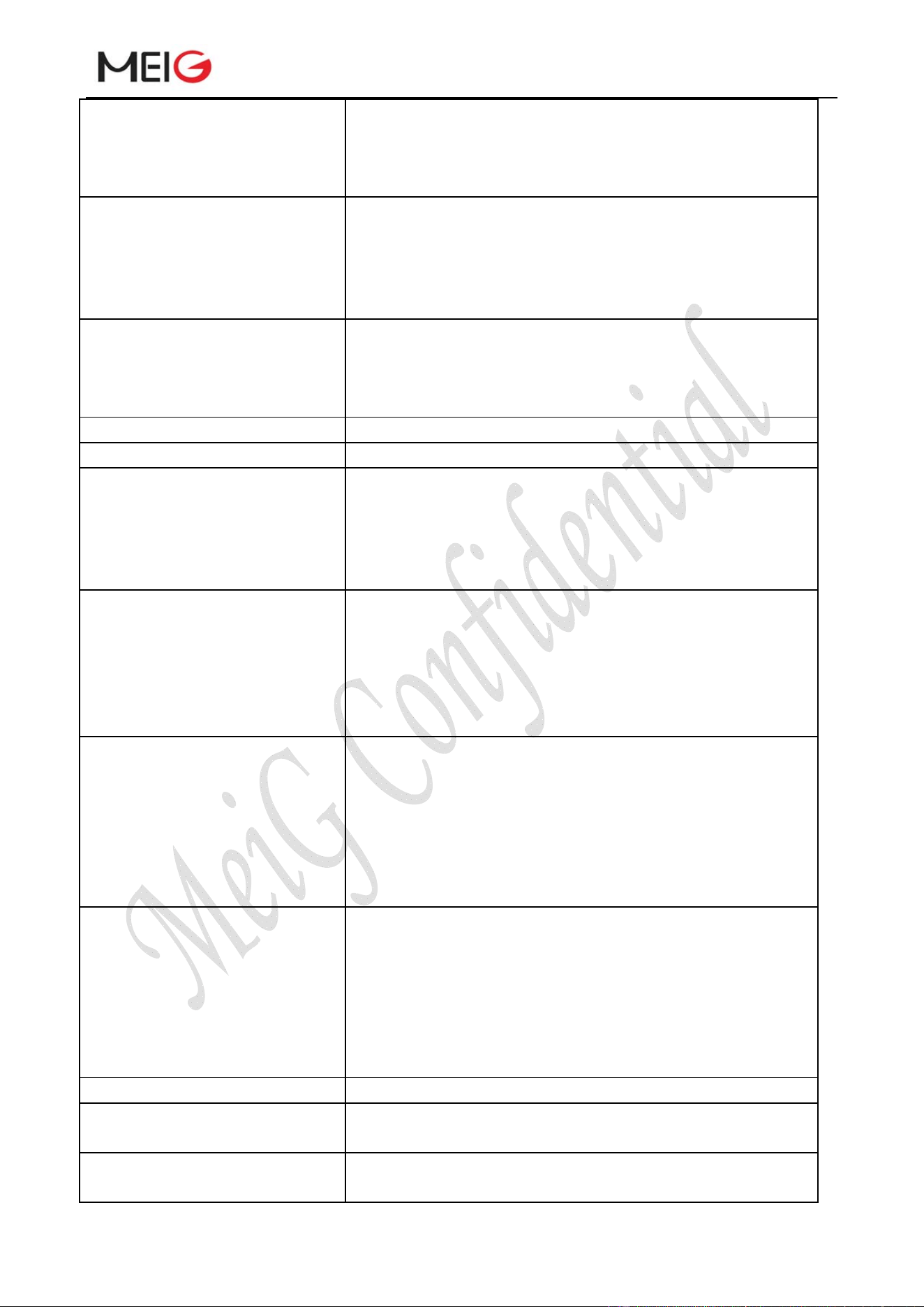
Table 3: List of main features of the module
Parameter Description
Power supply VBAT supply voltage range: 3.3V~4.2V
Typical supply voltage: 3.8V
Transmit power Class 4 (33dBm±2dB) for GSM850
Class 4 (33dBm±2dB) for GSM900
Class 1 (30dBm±2dB) for DCS1800
Class 1 (30dBm±2dB) for PCS1900
Class E2 (27dBm±3dB) for GSM850 8-PSK
Class E2 (27dBm±3dB) for GSM900 8-PSK
Class E2 (26dBm±3dB) for DCS1800 8-PSK
Class E2 (26dBm±3dB) for PCS1900 8-PSK
Class 3 (24dBm±1dB) for CDMA BC0
Class 3 (23dBm±2dB) for WCDMA bands
Class 3 (23dBm±2dB) for TD-SCDMA bands
Class 3 (23dBm±2dB) for LTE FDD bands
Class 3 (23dBm±2dB) for TD-LTE bands
LTE features Maximum support non-CA CAT4
Support 1.4 ~ 20MHz RF bandwidth
Downlink supports multi-user MIMO
FDD: maximum uplink rate 50Mbps,maximum
downlink rate 150Mbps
TDD: maximum uplink rate 35Mbps,maximum
downlink rate 130Mbps
WCDMA features Support 3GPP R8 DC-HSPA+
Support 16-QAM,64-QAM and QPSK modulation
3GPP R6 CAT6 HSUPA: maximum uplink rate
5.76Mbps
3GPP R8 CAT24 DC-HSPA+: maximum uplink rate
42Mbps
TD-SCDMA features Support CCSA Release3
Maximum uplink rate 2.2Mbps,maximum downlink rate
4.2Mbps
CDMA features Support CDMA 1X Advanced,1XEV-DOr0/-DOrA
maximum uplink rate 1.8Mbps,maximum downlink rate
3.1Mbps
GSM features R99:
CSD transmission rate: 9.6kbps,14.4kbps
GPRS:
Support GPRS multi-slot class 12(default 12)
Coding format: CS-1/CS-2/CS-3 and CS-4
Maximum 4 RX slots per frame
EDGE:
MeiGProductManualofSLM750Module
SLM750ModuleHardwareDesign Page 13, total 84 pages
Support EDGE multi-slot class 12(default 12)
Support GMSK and 8-PSK
Downlink coding format: CS 1-4 and MCS 1-9
Uplink coding format: CS 1-4 and MCS 1-9
Network protocol features Support
TCP/UDP/PPP/FTP/HTTP/SMTP/MMS/NTP/PING
/QMI protocol
Support PAP(Password Authentication Protocol)and
CHAP(Challenge Handshake Authentication Protocol)
Short message service Text and PDU mode
Point to point MO and MT
Short message cell broadcast
Short message storage: default stored in module
Multimedia message service AP terminal is required to realize MMS protocol
USIM card interface Support USIM/SIM card: 1.8V and 3V
Audio features Support 1 channel digital audio interface: PCM interface
GSM: HR/FR/EFR/AMR/AMR-WB
WCDMA: AMR/AMR-WB
LTE: AMR/AMR-WB
Support echo cancellation and noise suppression
PCM interface For audio use, need to connect the codec chip
Support 8 bit A-law, u-law and 16 bit Linear coding
format
Support long frame mode and short frame mode
Support master mode and slave mode, but in the long
frame it can only be used as the master mode
USB interface Compatible USB2.0 features (only support slave
mode),maximum data transfer rate reaches 480Mbps
Used for AT command, data transmission, GNSS NMEA
output, software debugging and software upgrading
USB drive: support Windows7, Windows8/8.1,
Windows10, Linux 2.6 or higher version, Android
2.3/4.0/4.2/4.4/5.0/5.1/6.0/7.0
Serial port Main serial port:
Used for AT commands and data transfer
Maximum baud rate is 3000000bps,default 115200bps
Support RTS and CTS hardware flow control
Debug serial port:
Used for Linux control, log output
Baud rate is 115200bps
RX-diversity Support LTE/WCDMA/CDMA RX-diversity
AT command Confirm to 3GPP TS 27.007, 27.005 and added new
MeiG AT commands
Network indication The two pins NET_STATUS,NET_MODE indicate the
network status
MeiGProductManualofSLM750Module
SLM750ModuleHardwareDesign Page 14, total 84 pages
Antenna interface Include main antenna(ANT_MAIN),RX-D diversity
antenna(ANT_DIV) and GNSS antenna(ANT_GNSS)
Physical features
Size: 32.0×29.0×2.4mm
Weight: <5 g
Temperature range Normal operating temperature: -30℃~+75℃
Limited operating temperature: -40℃~+85℃
Storage temperature: -45℃~+90℃
Software upgrade USB interface
RoHS All hardware components fully comply with the EU
RoHS standard
Ambient humidity 5%~95%
ESD VBAT,GND: Air discharge ±10KV,Contact discharge
±5KV
Antenna interface: Air discharge ±8KV,Contact
discharge ±4KV
Other interface: Air discharge ±1KV,Contact discharge
±0.5KV
Interface 144Pin LCC interface
LCC function interface Power interface
USB2.0 High-Speed interface
UART interface
USIM/SIM card interface (support 3V、1.8V)
PCM interface
Hardware reset interface
Indicator light interface
Sleep control interface
Flight mode control interface
ADC interface
I2C interface
SGMII interface
SD card interface
WLAN interface
BT_UART interface
USB_BOOT interface
2.3 Functional diagram
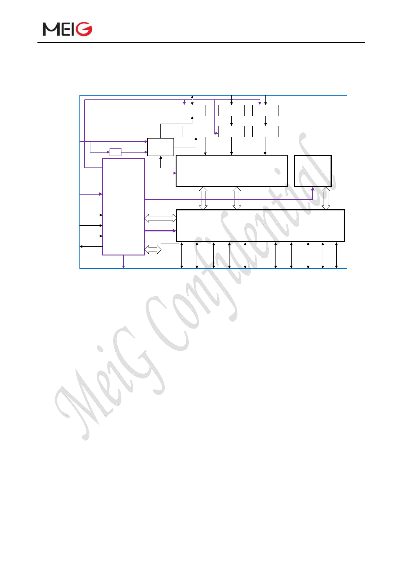
The following figure shows a block diagram of SLM750 and illustrates the major functional
parts.
Power management
Baseband chip
DDR+NAND storage
MeiGProductManualofSLM750Module
SLM750ModuleHardwareDesign Page 15, total 84 pages
Radio frequency
Peripheral interface
30
Switch SAW Switch
ANT_MAIN ANT_GNSS
ANT_DIV
Dupl ex
PA
LNA
SAW
DRx
PRx
Tx
VBAT_RF
APT
VBAT_BB
PMIC
PWR KEY
RESET_N
ADCs
STATUS
Control
19.2M
XO
VDD_EXT USB USIM
PCM I2C UAR Ts WLAN BT GPIOs SD SGMII
Baseband
Transceiver
NAND
DDR2
SDRAM
Control
IQ
Figure 1 Functional Diagram
2.4 Evaluation Board
In order to help you develop applications with SLM750, MeiG supplies an evaluation board,
Which contains USB data cable, antenna and other peripherals to control or test the module.
See MeiG_U_EVB User Guide for specific usage of evaluation board.

MeiGProductManualofSLM750Module
SLM750ModuleHardwareDesign Page 16, total 84 pages
3 Application Interface
3.1 General Description
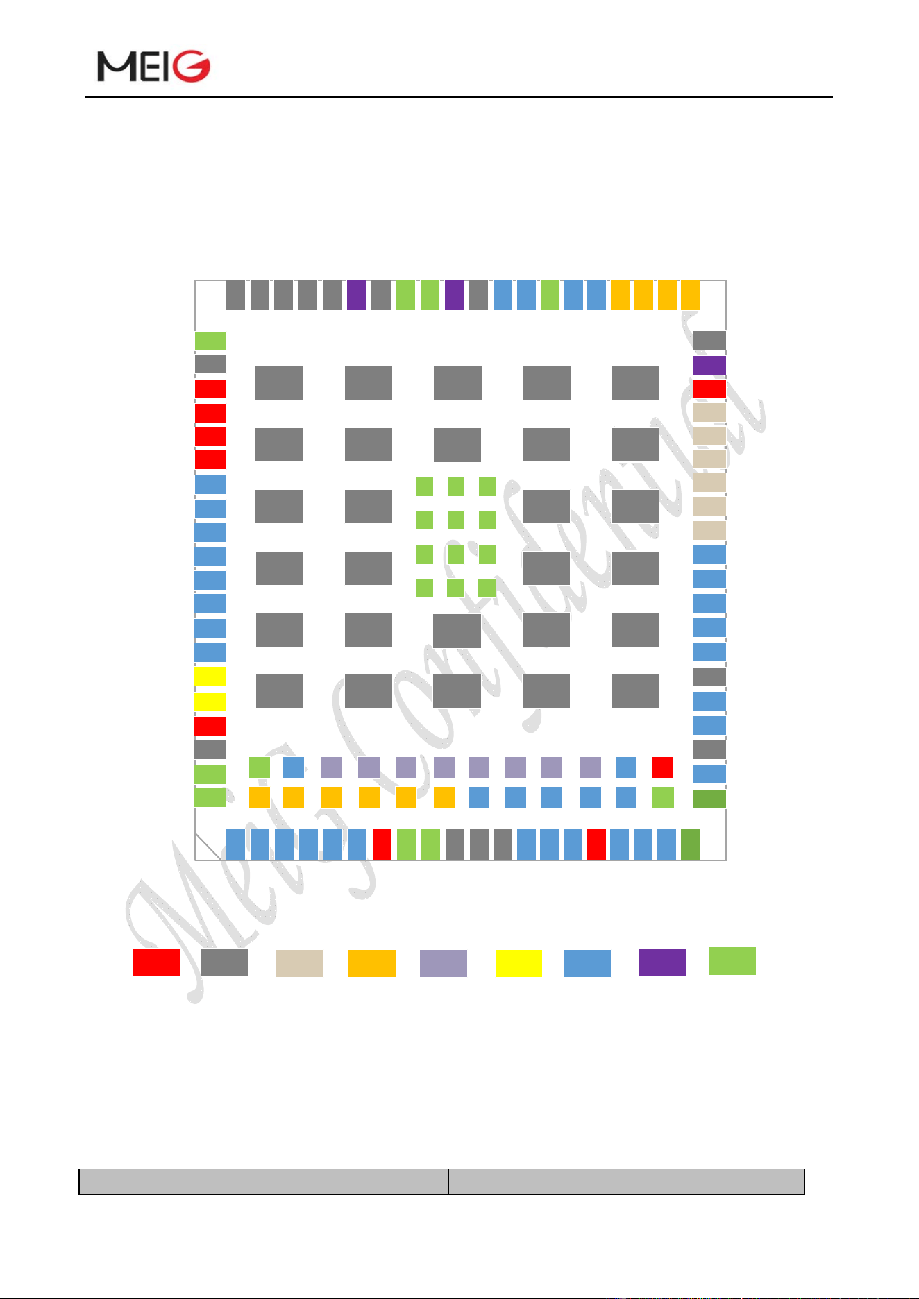
SLM750 uses LCC+LGA interface with a total of 144 PIN among which there are 80 LCC
pins and 64 LGA pins, providing the following function interface:
Power interface
USIM/SIM interface
USB interface
UART interface
PCM interface
I2C interface
Hardware reset interface
Status indication interface
Sleep control interface
Flight mode control interface
ADC interface
SGMII interface
SD card interface
WLAN interface
BT_UART interface
USB_BOOT interface
MeiGProductManualofSLM750Module
SLM750ModuleHardwareDesign Page 17, total 84 pages
3.2 LCC Card Interface Definition
52 51 50 49 48
144 143
47 46 45 44 43 42 41 40 39 38 37
1 2 3 4 5 6 7
141 142
8 9 10 11 12 13 14 15 16
69
68
67
66
65
64
63
114
113
72
71
70
23
24
25
26
27
28
29
116
115
19
20
21
22
GNDPOWER
WLAN&BT USBSGMII Signals
ANT
Reserved
GND
GND
GND
ANT_MAIN
GND
Reserved
Reserved
GND
ADC0
ADC1
Reserved
I2C_SDA
I2C_SCL
BT_CTS
BT_TXD
BT_RTS
SD_DATA2
SD_DATA3
PCM_CLK
PCM_SYNC
PCM_OUT
USB_BOOT
Reserved
USIM_CLK
USIM_DATA
GND
USIM_GND
USIM_PRESENCE
USIM_VDD
GND
DBG_RXD
DBG_TXD
Reserved
VDD_EXT
NET_STATUS
NET_MODE
W_DISABLE#
WAK EUP_OUT_N
AP_READY
WAKEU P_IN
Reserved
GND
USB_VBUS
RXD
TXD
DCD
Reserved
CT S
USB_DP
DTR
RTS
USB_DM
17 18
36
35
34
33
32
31
30
GND
ANT_DIV
VDD_SDIO
SD_CMD
SD_CLK
SD_DATA0
61
60
59
58
57
56
55
62
54 53
USIM_RST
SD_DATA1
PCM_IN
SD_INS_DET
GND
PWRKEY
RESET_N
GND
ANT_GNSS
GND
GND
RI
VBAT_BB
VBAT_BB
GND
Reserved
VBAT_RF
VBAT_RF
ST ATUS
85 86 87 88 89
73
90 91
92
93 94
95 96 97 98
99
100 101
102
103 104
105
106
107
108 109 110 111 112
74 75
76
79
82
129 130 131 132 133 134 13 5 136 137 138 139 140
77 78
80 81
83 84
117 118 119 120 12 1 12 2 12 3 12 4 12 5 126 127 128
BT_RXD
Reserved
WLAN_SLP_CLK
EPHY_RST_N
EPH Y_INT _N
SGMI I_MDATA
SGMII_MCLK
SGMII_TX_M
SGMII_TX_P
SGMII_RX_P
SGMII_RX_M
PM_ENABLE
USIM2_VDD
SDC1_DATA3
SDC1_DATA2
SDC1_DATA1
SDC1_DATA0
SDC1_CLK
SDC1_CMD
WA KE_ON_
WIRELESS
WLAN_EN
COEX_UART_RX
COEX_UART_TX
BT_EN
SD
Reserved
Reserved
Reserved
Figure 2 Pin Assignment
3.3 Pin Description
The following table shows the SLM750’s pin definition.
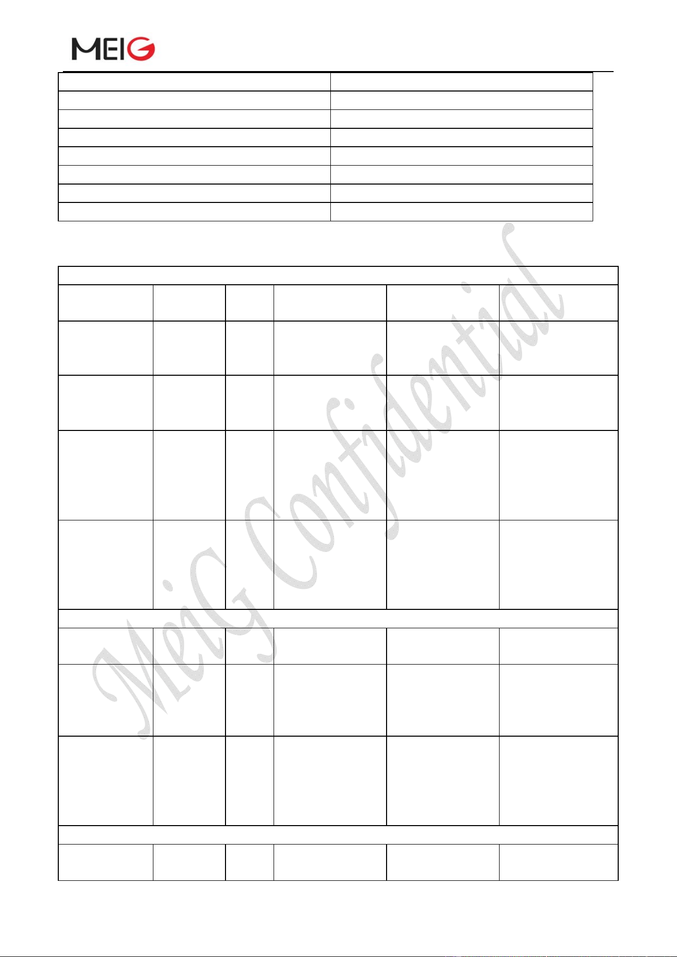
Table 4: IO Parameters Definition
Type Description
MeiGProductManualofSLM750Module
SLM750ModuleHardwareDesign Page 18, total 84 pages
IO Input output
DI Digital input
DO Digital output
PI Power input
PO Power output
AI Analog input
AO Analog output
OD Open drain
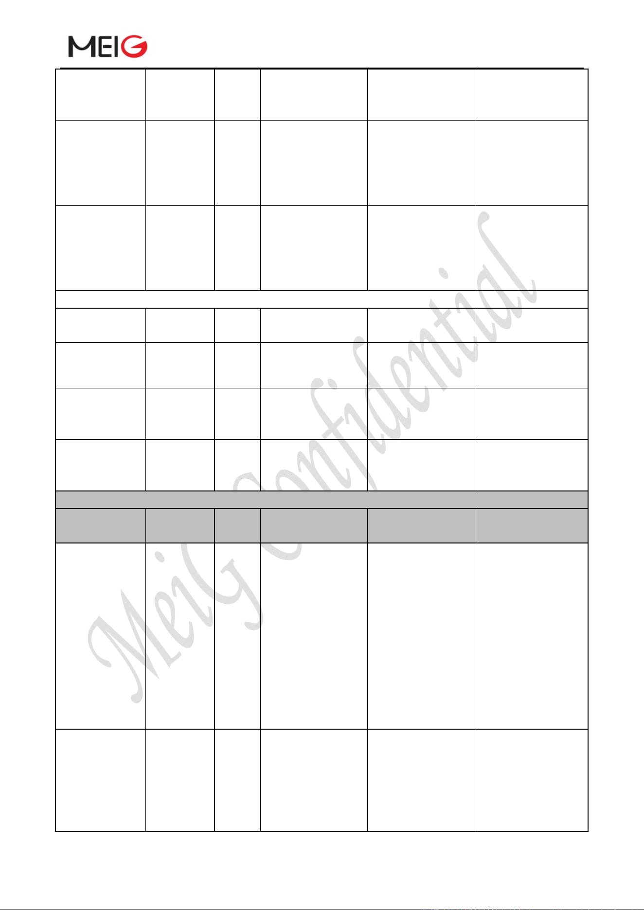
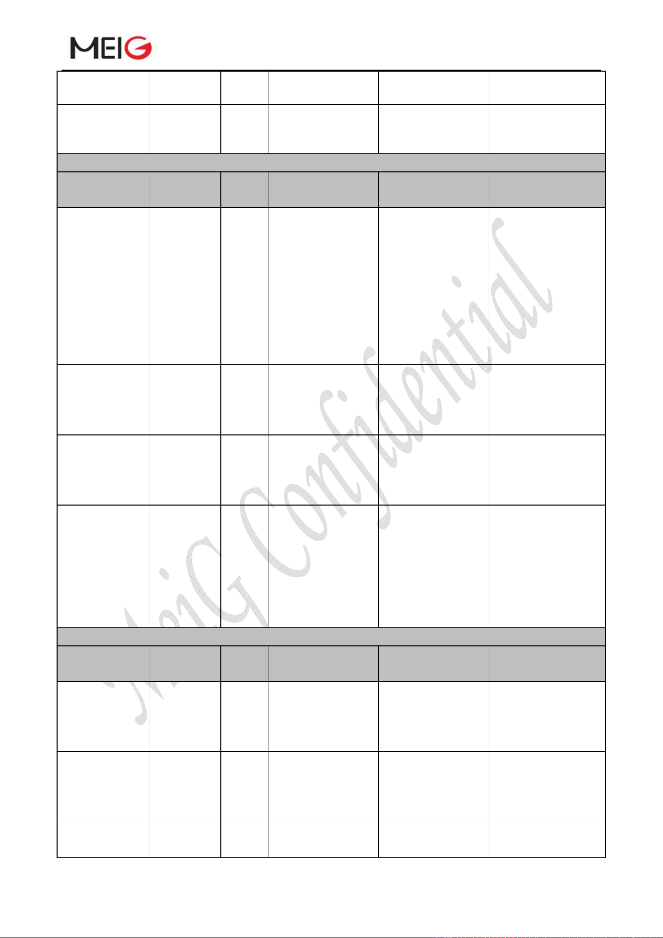
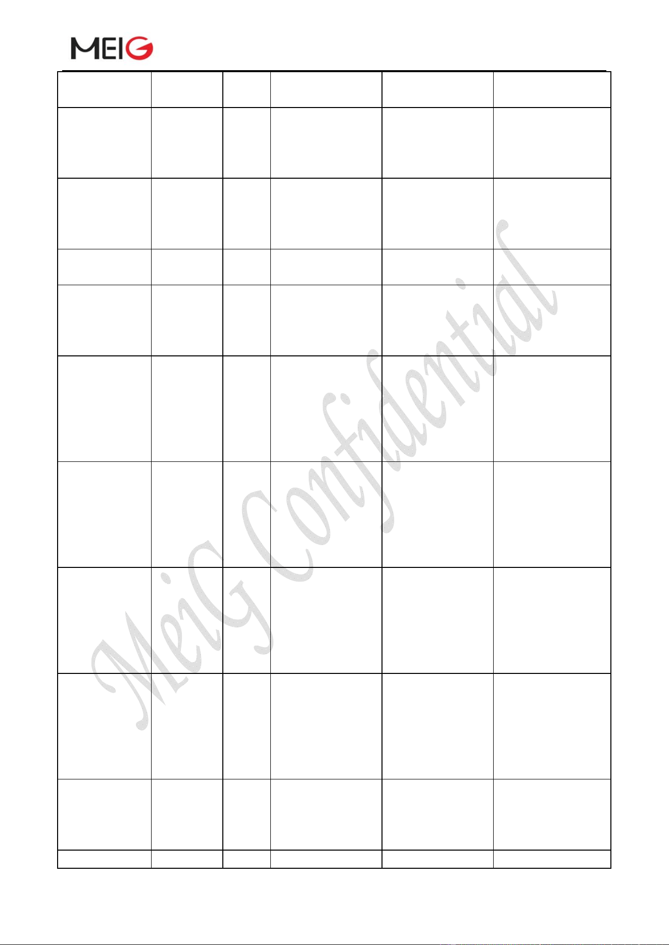
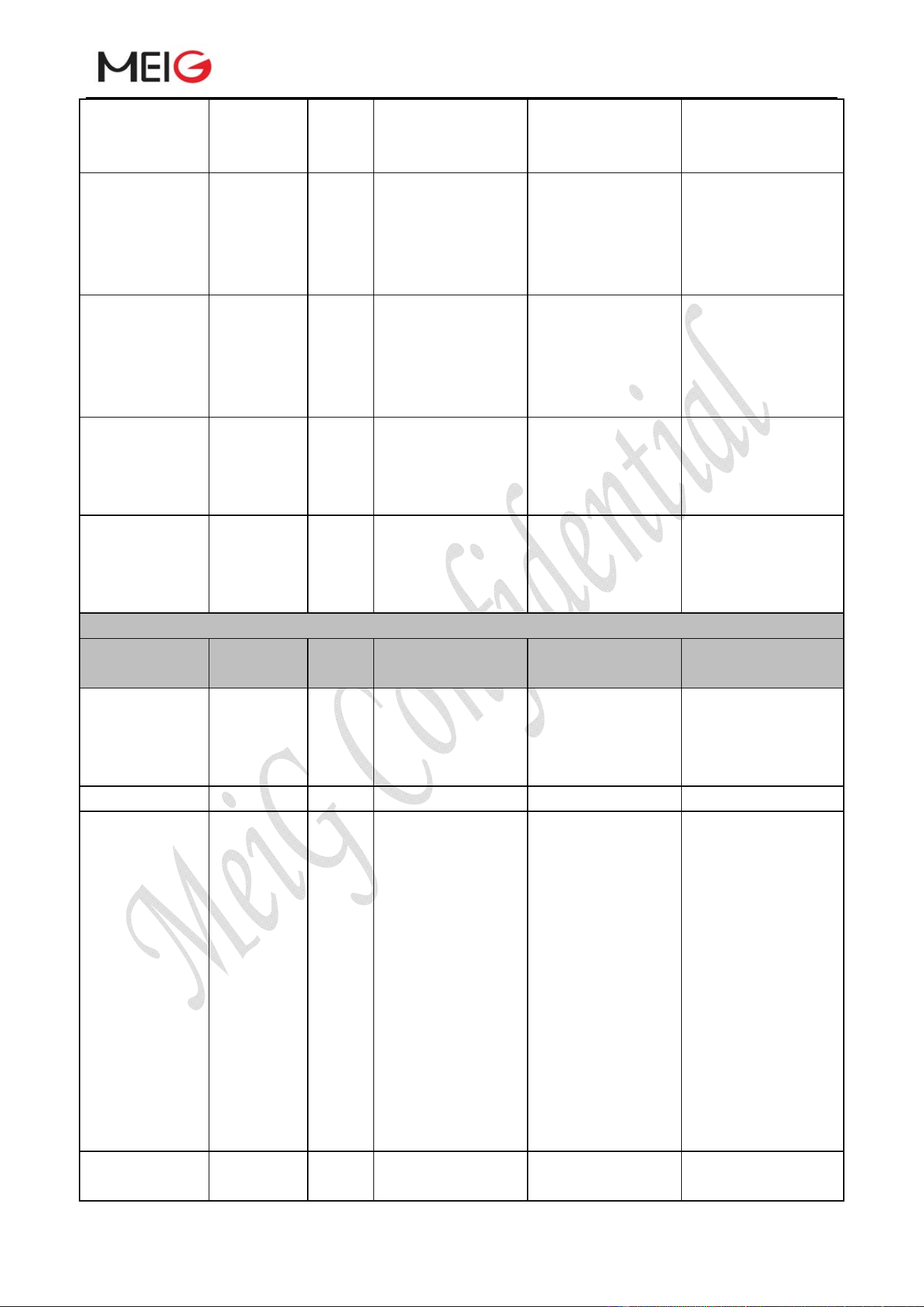
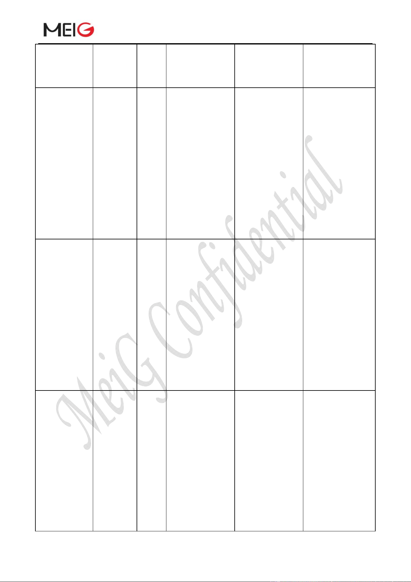
Table 5: Pin description
Power Supply
Pin name Pin
number
I/O Description DC features Note
VBAT_BB 59,60 PI Power supply for
module baseband
Vmax=4.2V
Vmin=3.3V
Vnorm=3.8V
It must be able to
provide sufficient
current up to 1A
VBAT_RF 57,58 PI Power supply for
module RF
Vmax=4.2V
Vmin=3.3V
Vnorm=3.8V
It must be able to
provide sufficient
current up to 2A
VDD_EXT
7 PO 1.8V output Vnorm=1.8V
I
o
max=80mA
Power supply for
external GPIO’s
pull up circuits;
If unused, keep it
open
GND 8,9,19,22,
36,46,48,
50~54,
56,72,
85~112
- Ground - -
Turn on/off
Pin name Pin
number
I/O Description DC features Note
RESET_N 20 DI Reset the module V
IH
max=2.1V
V
IH
min=1.3V
V
IL
max=0.5V
1.8V power
domain; active low
level. If unused,
keep it open
PWRKEY 21 DI
Turn on/Standby
V
IH
max=2.1V
V
IH
min=1.3V
V
IL
max=0.5V
Diode voltage drop
inside Qualcomm
chip results in
0.8V output of the
pin
Module status indication
Pin name Pin
number
I/O Description DC features Note
MeiGProductManualofSLM750Module
SLM750ModuleHardwareDesign Page 19, total 84 pages
STATUS
61 OD Indicate the
module operating
status
Driving current
should be less
than 0.9mA
Require external
pull-up. If unused,
keep it open
NET_MODE
5 OD Indicate the
module network
registration status
VOHmin=1.35V
VOLmax=0.45V
1.8V power
domain, require
external pull-up. If
unused, keep it
open
NET_STATU
S
6 OD Indicate the
module network
running status
VOHmin=1.35V
VOLmax=0.45V
1.8V power
domain, require
external pull-up. If
unused, keep it
open
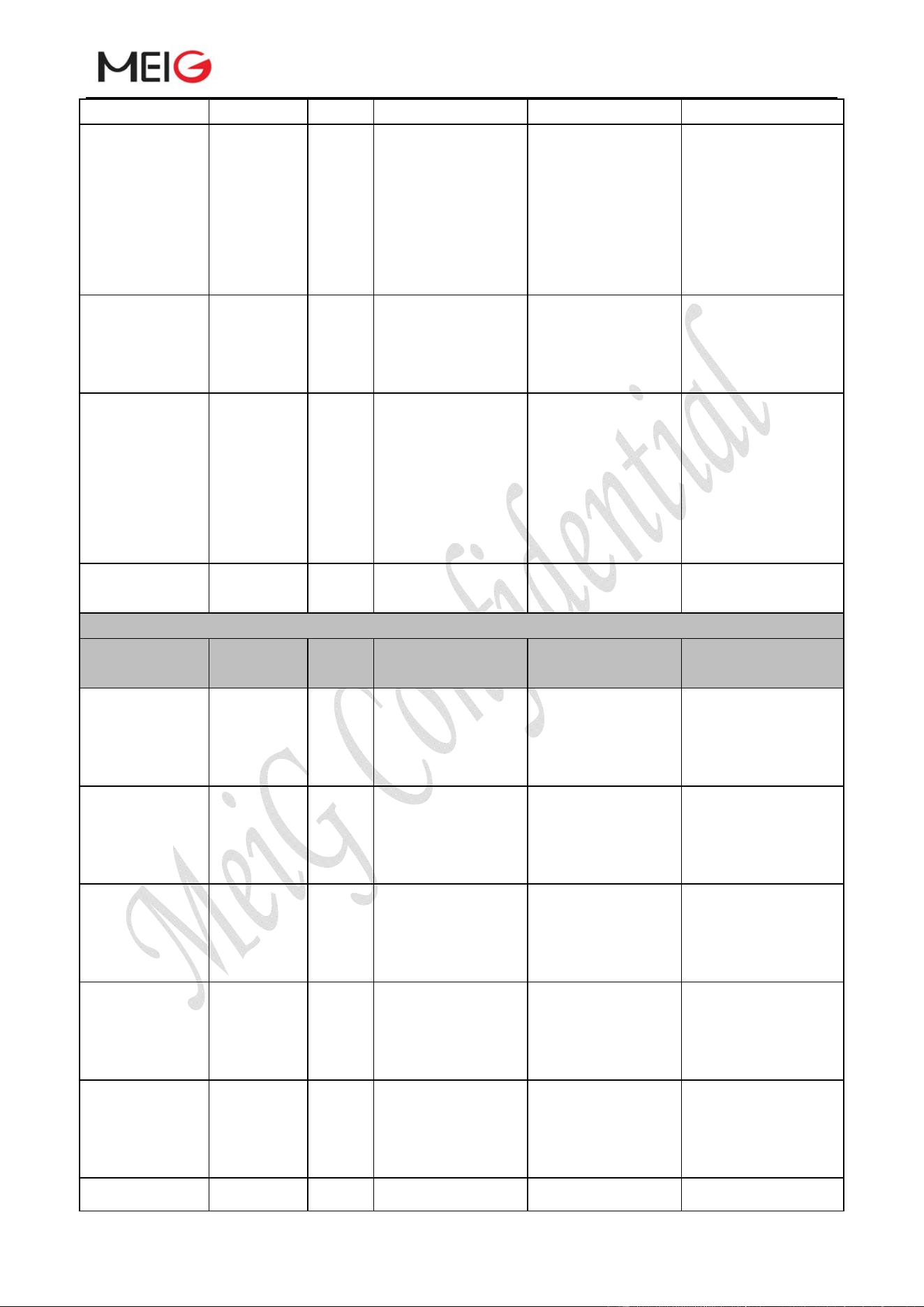
USB interface
Pin name Pin
number
I/O Description DC features Note
USB_VBUS
71 PI USB detection
Vmax=5.25V
Vmin=3.0V
Vnorm=5.0V
USB_DP 69 IO USB differential
data positive
signal
Compliant with
USB2.0 standard
specification
Require
differential
impedance of 90Ω
USB_DM 70 IO USB differential
data negative
signal
Compliant with
USB2.0 standard
specification
Require
differential
impedance of 90Ω
USIM card interface
Pin name Pin
number
I/O Description DC features Note
USIM_DATA 15 IO USIM card data
bus
1.8V USIM:
V
IL
max=0.6V
V
IH
min=1.2V
V
OL
max=0.45V
V
OH
min=1.35V
3.0V USIM:
V
IL
max=1.0V
V
IH
min=1.95V
V
OL
max=0.45V
V
OH
min=2.55V
-
USIM_CLK 16 DO USIM card clock
line
1.8V USIM:
V
OL
max=0.45V
V
OH
min=1.35V
3.0V USIM:
V
OL
max=0.45V
-
MeiGProductManualofSLM750Module
SLM750ModuleHardwareDesign Page 20, total 84 pages
V
OH
min=2.55V
USIM_RST 17 DO USIM card reset
line
1.8V USIM:
V
OL
max=0.45V
V
OH
min=1.35V
3.0V USIM:
V
OL
max=0.45V
V
OH
min=2.55V
-
USIM_PRESE
NCE
13 DI USIM card
detection
V
IL
min=-0.3V
V
IL
max=0.6V
V
IH
min=1.2V
V
IH
max=2.0V
1.8Vpower
domain, require
external pull-up to
1.8V
USIM_VDD 14 PO USIM card
supply voltage
1.8V USIM:
Vmax=1.9V
Vmin=1.7V
3.0V USIM:
Vmax=3.05V
Vmin=2.7V
I
o
max=50mA
Either 1.8V or
3.0V USIM card is
identified by the
module
automatically
USIM_GND 10 USIM card
ground
Connect with
module ground
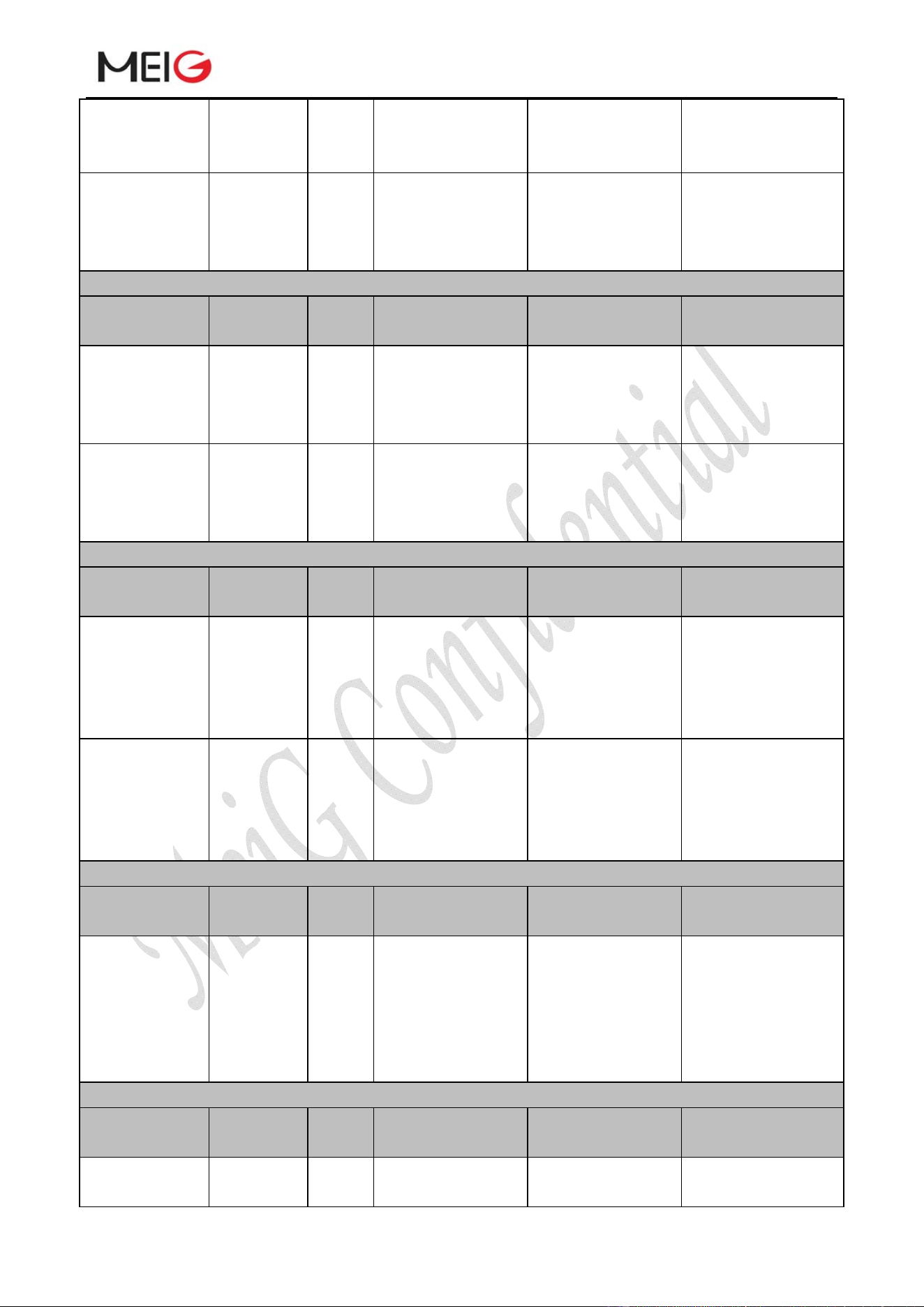
Main serial port
Pin name Pin
number
I/O Description DC features Note
RI 62 DO Ring indicator VOLmax=0.45V
VOHmin=1.35V
1.8V power
domain.
If unused, keep
it open.
DCD 63 DO Carrier detect VOLmax=0.45V
VOHmin=1.35V
1.8V power
domain.
If unused, keep
it open.
DTR 66 DI DTE ready, sleep
mode control
VILmin=-0.3V
VILmax=0.6V
VIHmin=1.2V
VIHmax=2.0V
1.8V power
domain.
If unused, keep
it open.
RXD 68 DI Receive data VILmin=-0.3V
VILmax=0.6V
VIHmin=1.2V
VIHmax=2.0V
1.8V power
domain.
If unused, keep
it open.
TXD 67 DO Transmit data VOLmax=0.45V
VOHmin=1.35V
1.8V power
domain.
If unused, keep
it open.
CTS 64 DI Clear to send VOLmax=0.45V 1.8V power
MeiGProductManualofSLM750Module
SLM750ModuleHardwareDesign Page 21, total 84 pages
VOHmin=1.35V domain.
If unused, keep
it open.
RTS 65 DO DTE requires to
transmit data
VILmin=-0.3V
VILmax=0.6V
VIHmin=1.2V
VIHmax=2.0V
1.8V power
domain.
If unused, keep
it open.
Debug serial port
Pin name Pin
number
I/O Description DC features Note
DBG_TXD 12 DO Transmit data V
OL
max=0.45V
V
OH
min=1.35V
1.8V power
domain.
If unused, keep
it open.
DBG_RXD 11 DI Receive data V
IL
min=-0.3V
V
IL
max=0.6V
V
IH
min=1.2V
V
IH
max=2.0V
1.8V power
domain.
If unused, keep
it open.
ADC interface
Pin name Pin
number
I/O Description DC features Note
ADC0
45 AI General
purpose
analog to
digital
converter.
Voltage range:
0.05V~1.8V
If unused, keep it
open.
ADC1
44 AI General
purpose
analog to
digital
converter.
Voltage range:
0.05V~1.8V
If unused, keep it
open.
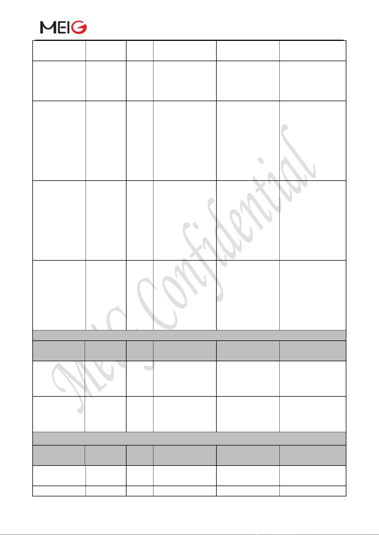
USB_BOOT interface
Pin name Pin
number
I/O Description DC features Note
USB_BOOT 115
DI
Forced
download
mode control
VOLmax=0.45
VOHmin=1.35V
1.8V power
domain. Active
high level.
Suggested
reservation of test
point.
PCM interface
Pin name Pin
number
I/O Description DC features Note
PCM_IN 24 DI PCM data input V
IL
min=-0.3V
V
IL
max=0.6V
1.8V power
domain.
MeiGProductManualofSLM750Module
SLM750ModuleHardwareDesign Page 22, total 84 pages
V
IH
min=1.2V
V
IH
max=2.0V
If unused, keep
it open.
PCM_OUT 25 DO PCM data output V
OL
max=0.45V
V
OH
min=1.35V
1.8V power
domain.
If unused, keep
it open.
PCM_CLK 27 IO PCM clock V
OL
max=0.45V
V
OH
min=1.35V
V
IL
min=-0.3V
V
IL
max=0.6V
V
IH
min=1.2V
V
IH
max=2.0V
1.8V power
domain. In master
mode, it is an
output signal. In
slave mode, it is an
input signal. If
unused, keep it
open.
PCM_SYNC 26 IO PCM data
synchronous
signal
V
OL
max=0.45V
V
OH
min=1.35V
V
IL
min=-0.3V
V
IL
max=0.6V
V
IH
min=1.2V
V
IH
max=2.0V
1.8V power
domain. In master
mode, it is an
output signal. In
slave mode, it is an
input signal. If
unused, keep it
open.
CDC_I2S_MC
LK
116 DO 19.2MHz signal
clock
Module
outputs19.2MHz
clock signal, which is
used to provide to the
external CODEC,
If
unused, keep it
open.
I2C interface
Pin name Pin
number
I/O Description DC features Note
I2C_SCL
41 OD
I2C serial clock
Require
external pull-up to
1.8V. If unused,
keep it open.
I2C_SDA
42 OD
I2C serial data
Require
external pull-up to
1.8V. If unused,
keep it open.
RF Interface
Pin name Pin
number
I/O Description DC features Note
ANT_DIV
35 AI
Diversity antenna
50 ohm
impedance
If unused, keep it
open.
ANT_MAIN
49 IO
Main antenna 50 ohm
MeiGProductManualofSLM750Module
SLM750ModuleHardwareDesign Page 23, total 84 pages
impedance
ANT_GNSS
47 AI
GNSS antenna
50 ohm
impedance
If unused, keep it
open.
GPIO Pin
Pin name Pin
number
I/O Description DC features Note
WAKEUP_IN 1 DI Sleep mode input
control
V
IL
min=-0.3V
V
IL
max=0.6V
V
IH
min=1.2V
V
IH
max=2.0V
1.8V power
domain.
High level wakes
up the module; in
low level the
module enters into
sleep mode. If
unused, keep it
open.
AP_READY 2 DI
Application
processor sleep
state detection
V
OL
max=0.45V
V
OH
min=1.35V
1.8V power
domain.
If unused, keep it
open.
WAK EU P_ O
UT_N
3 DO Sleep mode
output
VOLmax=0.45V
VOHmin=1.35V
1.8V power
domain.
If unused, keep it
open.
W_DISABLE
#
4 DI Flight mode
control
V
IL
min=-0.3V
V
IL
max=0.6V
V
IH
min=1.2V
V
IH
max=2.0V
1.8V power
domain.
In low level the
module enters into
flight mode. If
unused, keep it
open.
WLAN interface
Pin name Pin
number
I/O Description DC features Note
BT_RTS* 37 DO
Bluetooth serial
port request to
send data
VILmin=-0.3V
VILmax=0.6V
VIHmin=1.2V
VIHmax=2.0V
1.8V power
domain.
If unused, keep it
open.
BT_TXD* 38 DO
Bluetooth serial
port sends data
VOLmax =0.45V
VOHmin =1.35V
1.8V power
domain.
If unused, keep it
open.
BT_RXD* 39 DI
Bluetooth Serial
Port receives data
VILmin=-0.3V
VILmax=0.6V
1.8V power
domain.
MeiGProductManualofSLM750Module
SLM750ModuleHardwareDesign Page 24, total 84 pages
VIHmin=1.2V
VIHmax=2.0V
If unused, keep it
open.
BT_CTS* 40 DI
Bluetooth serial
sending clearance
VOLmax =0.45V
VOHmin =1.35V
1.8V power
domain.
If unused, keep it
open.
BT_EN* 139 DO
Bluetooth enables VOLmax =0.45V
VOHmin =1.35V
1.8V power
domain.
If unused, keep it
open.
WLAN_SLP_C
LK
118 DO
WLAN sleep
clock
If unused, keep it
open.
PM_ENABLE 127 DO External power
supply enables
control
VOLmax =0.45V
VOHmin =1.35V
1.8V power
domain.
If unused, keep it
open.
SDC1_DATA3 129 IO WLAN SDIO
signal data line 3
VOLmax=0.45
VOHmin=1.35V
V ILmin=-0.3V
VILmax=0.6V
VIHmin=1.2V
VIHmax =2.0V
1.8V power
domain.
If unused, keep it
open.
SDC1_DATA2 130 IO WLAN SDIO
signal data line 2
VOLmax=0.45
VOHmin=1.35V
V ILmin=-0.3V
VILmax=0.6V
VIHmin=1.2V
VIHmax =2.0V
1.8V power
domain.
If unused, keep it
open.
SDC1_DATA1 131 IO WLAN SDIO
signal data line 1
VOLmax=0.45
VOHmin=1.35V
V ILmin=-0.3V
VILmax=0.6V
VIHmin=1.2V
VIHmax =2.0V
1.8V power
domain.
If unused, keep it
open.
SDC1_DATA0 132 IO WLAN SDIO
signal data line 0
VOLmax=0.45
VOHmin=1.35V
V ILmin=-0.3V
VILmax=0.6V
VIHmin=1.2V
VIHmax =2.0V
1.8V power
domain.
If unused, keep it
open.
SDC1_CLK 133 DO WLAN SDIO
signal clock
VOLmax=0.45
VOHmin=1.35V
1.8V power
domain.
If unused, keep it
open.
SDC1_CMD 134 DO WLAN SDIO VOLmax=0.45 1.8V power
MeiGProductManualofSLM750Module
SLM750ModuleHardwareDesign Page 25, total 84 pages
instruction signal VOHmin=1.35V domain.
If unused, keep it
open.
WAKE_ON_
WIRELESS
135 DI WLAN wakes the
module
V ILmin=-0.3V
VILmax=0.6V
VIHmin=1.2V
VIHmax =2.0V
1.8V power
domain. Active
low level.
If unused, keep it
open.
WLAN_EN 136 DO WLAN enables VOLmax=0.45
VOHmin=1.35V
1.8V power
domain. Active
high level.
If unused, keep it
open.
COEX_UART
_RXD
137 DI LTE/WLAN&BT
coexistence signal
V ILmin=-0.3V
VILmax=0.6V
VIHmin=1.2V
VIHmax =2.0V
1.8V power
domain.
If unused, keep it
open.
COEX_UART
_TXD
138 DO LTE/WLAN&BT
coexistence signal
VOLmax=0.45
VOHmin=1.35V
1.8V power
domain.
If unused, keep it
open.
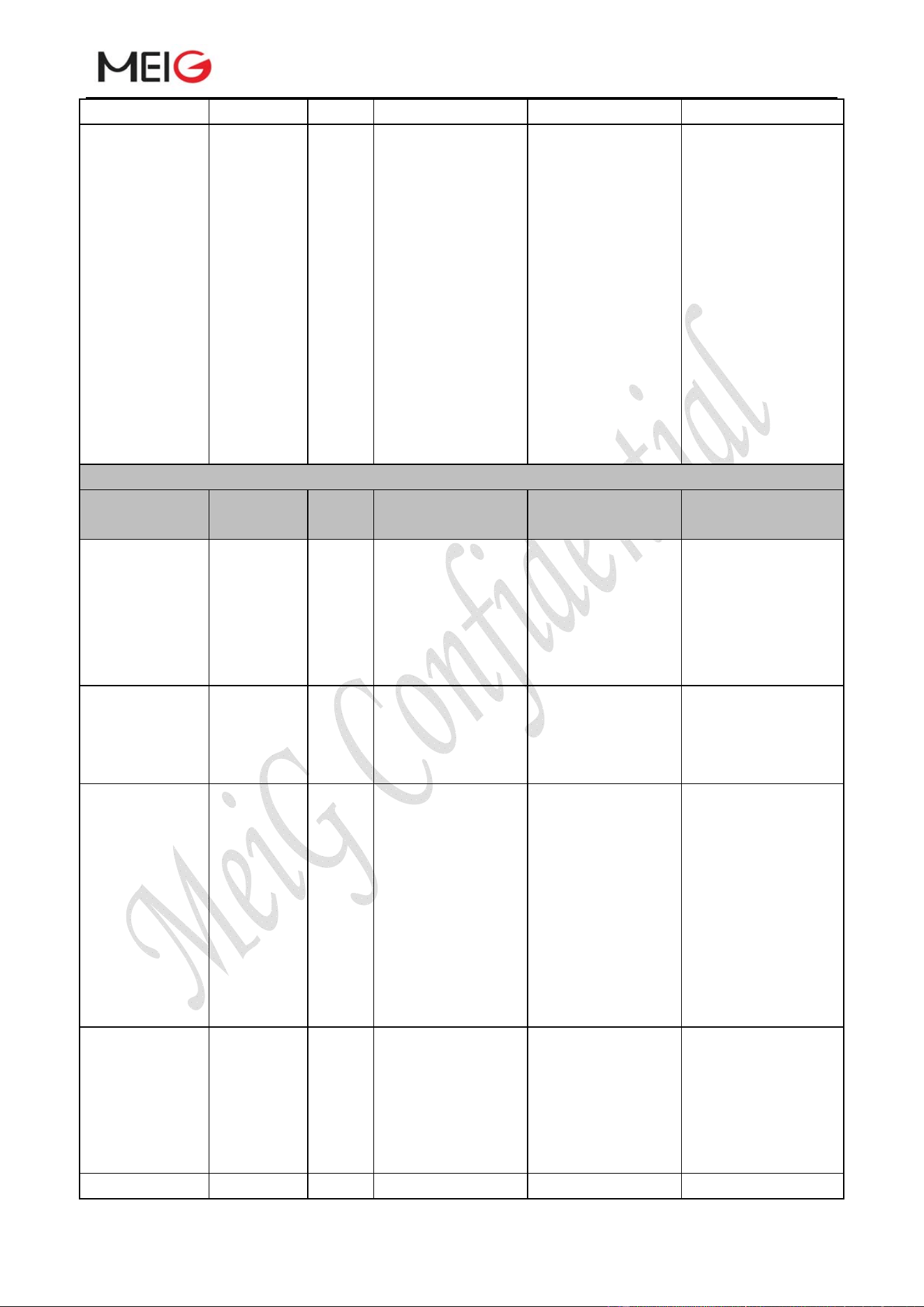
SD card Interface
Pin name Pin
number
I/O Description DC features Note
SD_INS_DET 23 DI VILmin=-0.3V
VILmax=0.6V
VIHmin=1.2V
VIHmax =2.0V
1.8V power
domain.
If unused, keep it
open
VDD_SDIO 34 PO IOmax =50mA
SD_CMD 33 IO SD card SDIO
instruction signal
1.8V SD card:
VOLmax=0.45
VOHmin=1.4V
V ILmin=-0.3V
VILmax=0.58V
VIHmin=1.27V
VIHmax =2.0V
3.0V SD card:
VOLmax=0.38V
VOHmin=2.01V
V ILmin=-0.3V
VILmax=0.76V
VIHmin=1.72V
VIHmax=3.34V
Refer to SD3.0
protocol. If
unused, keep it
open.
SD_CLK 32 DO SD card SDIO
signal clock
1.8V SD card:
VOLmax=0.45V
Refer to SD3.0
protocol. If
MeiGProductManualofSLM750Module
SLM750ModuleHardwareDesign Page 26, total 84 pages
VOHmin =1.4V
3.0V SD card:
VOLmax=0.38V
VOHmin=2.01V
unused, keep it
open.
SD_DATA3 28 IO SD card SDIO
signal data line 3
1.8V SD card:
VOLmax=0.45
VOHmin=1.4V
V ILmin=-0.3V
VILmax=0.58V
VIHmin=1.27V
VIHmax =2.0V
3.0V SD card:
VOLmax=0.38V
VOHmin=2.01V
V ILmin=-0.3V
VILmax=0.76V
VIHmin=1.72V
VIHmax=3.34V
Refer to SD3.0
protocol. If
unused, keep it
open.
SD_DATA2 29 IO SD card SDIO
signal data line 2
1.8V SD card:
VOLmax=0.45
VOHmin=1.4V
V ILmin=-0.3V
VILmax=0.58V
VIHmin=1.27V
VIHmax =2.0V
3.0V SD card:
VOLmax=0.38V
VOHmin=2.01V
V ILmin=-0.3V
VILmax=0.76V
VIHmin=1.72V
VIHmax=3.34V
Refer to SD3.0
protocol. If
unused, keep it
open.
SD_DATA1 30 IO SD card SDIO
signal data line 1
1.8V SD card:
VOLmax=0.45
VOHmin=1.4V
V ILmin=-0.3V
VILmax=0.58V
VIHmin=1.27V
VIHmax =2.0V
3.0V SD card:
VOLmax=0.38V
VOHmin=2.01V
V ILmin=-0.3V
VILmax=0.76V
VIHmin=1.72V
Refer to SD3.0
protocol. If
unused, keep it
open.
MeiGProductManualofSLM750Module
SLM750ModuleHardwareDesign Page 27, total 84 pages
VIHmax=3.34V
SD_DATA0 31 IO SD card SDIO
signal data line 0
1.8V SD card:
VOLmax=0.45
VOHmin=1.4V
V ILmin=-0.3V
VILmax=0.58V
VIHmin=1.27V
VIHmax =2.0V
3.0V SD card:
VOLmax=0.38V
VOHmin=2.01V
V ILmin=-0.3V
VILmax=0.76V
VIHmin=1.72V
VIHmax=3.34V
Refer to SD3.0
protocol. If
unused, keep it
open.
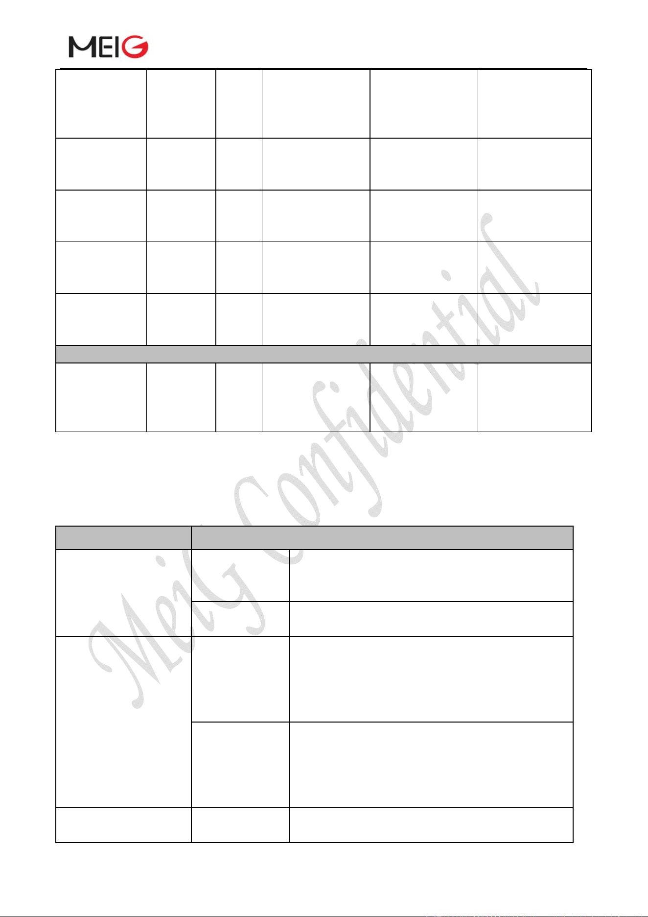
SGMII Pin
Pin name Pin
number
I/O Description DC features Note
EPHY_RST_
N*
119 DO Ethernet PHY
reset
For 1.8V:
VOLmax=0.45V
VOHmin=1.4V
For 2.85V:
VOLmax=0.35V
VOHmin =2.14V
1.8V /2.85V power
domain.
If unused, keep it
open.
EPHY_INT_N
*
120 DI Ethernet PHY
interruption
VILmin=-0.3V
VILmax=0.6V
VIHmin=1.2V
VIHmax=2.0V
1.8V /2.85V power
domain.
If unused, keep it
open.
SGMII_MDA
TA*
121 IO SGMII MDIO
data
For 1.8V:
VOLmax=0.45V
VOHmin=1.4V
VILmax =0.58V
VIHmin =1.27V
For 2.85V:
VOLmax=0.35V
VOHmin =2.14V
VILmax =0.71V
VIHmin =1.78V
1.8V/2.85V power
domain.
If unused, keep it
open.
SGMII_MCL
K*
122 DO SGMII MDIO
clock
For 1.8V:
VOLmax=0.45V
VOHmin=1.4V
For 2.85V:
VOLmax=0.35V
VOHmin =2.14V
USIM2_VDD 128 PO SGMII MDIO - 1.8V/2.85V power
MeiGProductManualofSLM750Module
SLM750ModuleHardwareDesign Page 28, total 84 pages
* power supply domain, require
external pull-up
level for SGMII
SDIO Pin
SGMII_TX_
M*
123 AO SGMII data
transmit negative
signals
- If unused, keep it
open.
SGMII_TX_P
*
124 AO SGMII data
transmit positive
signals
- If unused, keep it
open.
SGMII_RX_P
*
125 AI SGMII data
receive positive
signals
- If unused, keep it
open.
SGMII_RX_
M*
126 AI SGMII data
receive negative
signals
- If unused, keep it
open.
Reserved Pins
RESERVED
18, 43,55,
73~84,113,
114,117,
140~144
Reserved Keep it open
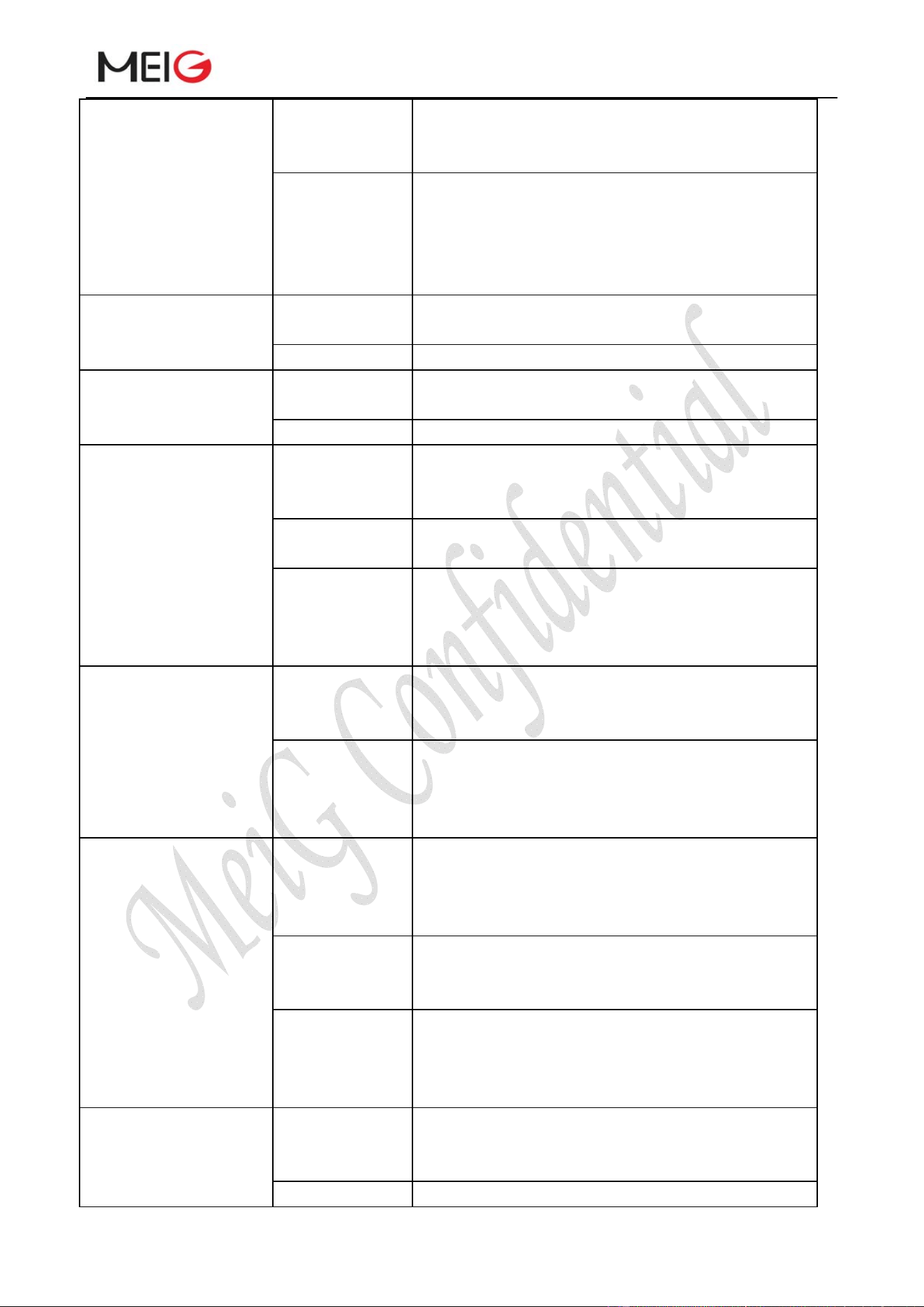
3.4 Operating Mode
Table 6: Overview of Operating Modes
Mode Description
GSM mode GSM IDLE The module is in idle state and has registered to the
GSM network, and it is ready to send and receive
data(SMS and voice service).
GSM TALK The module is ready for voice talk service; the
power consumption is decided by net setting.
GPRS mode GPRS IDLE The module is ready for GPRS data transfer. No
data sending or receiving at this time. The power
consumption is decided by net setting and related
settings of GPRS. (For example, multi slot Class
level settings)
GPRS DATA In GPRS data sending and receiving, the power
consumption is decided by net setting (eg. Power
control level), data uplink and downlink rat and
related settings of GPRS. (For example, multi slot
Class level settings)
EDGE Mode EDGE IDLE The module is ready for EDGE data transfer. No
data sending or receiving at this time. The power
MeiGProductManualofSLM750Module
SLM750ModuleHardwareDesign Page 29, total 84 pages
consumption is decided by net setting and related
settings of EDGE. (For example, multi slot Class
level settings)
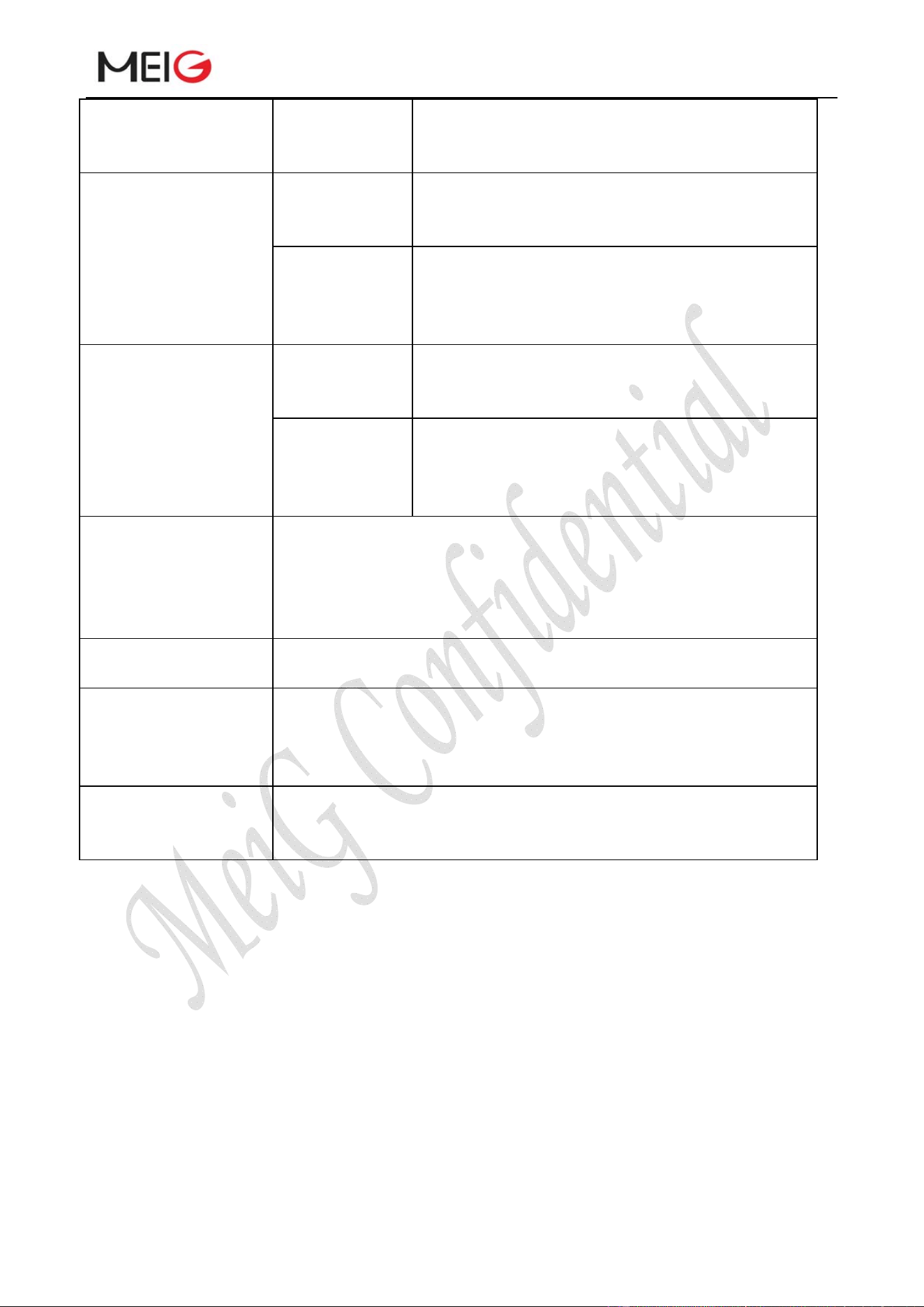
EDGE DATA In EDGE data sending and receiving, the power
consumption is decided by net setting (eg. Power
control level), data uplink and downlink rat and
related settings of EDGE. (For example, multi slot
Class level settings)
CDMA Mode CDMA IDLE The module is ready for CDMA voice and data
transfer. No data sending or receiving at this time.
CDMA DATA CDMA data transfer is ongoing.
EVDO Mode EVDO IDLE The module is ready for EVDO voice and data
transfer. No data sending or receiving at this time.
EVDO DATA EVDO data transfer is ongoing.
WCDMA Mode WCDMA IDLE The module system is in idle state and the module
has been registered to the WCDMA network, and it
is ready to send and receive services at this time
WCDMA
TALK
The module is in WCDMA voice service, the power
consumption is decided by net setting.
WCDMA
DATA
WCDMA data transfer is ongoing. The power
consumption is decided by net setting (eg. Power
control level), data uplink and downlink rate and
related settings of WCDMA.
HSPA Mode HSPA IDLE The module is ready for HSPA voice and data
transfer. No data sending or receiving at this time.
The power consumption is decided by net setting.
HSPA DATA HSPA data transfer is ongoing. The power
consumption is decided by net setting (eg. Power
control level), data uplink and downlink rate and
related settings of HSPA.
TD-SCDMA Mode TD-SCDMA
IDLE
The module system is in idle state and the module
has been registered to the TD-SCDMA network,
and it is ready to send and receive services at this
time.
TD-SCDMA
TALK
The module TD-SCDMA is in voice service, and
the power consumption is decided by network
settings
TD-SCDMA
DATA
TD-SCDMA data transfer is ongoing, the power
consumption is decided by net settings (eg. Power
control level), data uplink and downlink rate and
related settings of TD-SCDMA
TD-HSPA Mode TD-HSPA
IDLE
The module system is in idle state and the module
has been registered to the TD-HSPA network, and it
is ready to send and receive services at this time.
TD-HSPA TD-HSPA data transfer is ongoing, the power
MeiGProductManualofSLM750Module
SLM750ModuleHardwareDesign Page 30, total 84 pages
DATA consumption is decided by net settings(eg. Power
control level), data uplink and downlink rate and
related settings of TD-HSPA.
TD-LTE Mode TD-LTE IDLE The module is ready for TD-LTE data transfer. No
data sending or receiving at this time. The power
consumption is decided by net setting.
TD-LTE DATA TD-LTE data transfer is ongoing; the power
consumption is decided by net setting(eg. Power
control level), data uplink and downlink rate and
related settings of TD-LTE.
FDD LTE Mode FDD LTE IDLE The module is ready for FDD LTE data transfer. No
data sending or receiving at this time. The power
consumption is decided by net setting.
FDD LTE
DATA
FDD LTE data transfer is ongoing; the power
consumption is decided by net setting (eg. Power
control level), data uplink and downlink rate and
related settings of FDD LTE.
Minimum functionality
mode
AT+CFUN=0 command can set the module to enter into a minimum
functionality mode without removing the power supply of VBAT. At
this time RF is closed. Use AT+CFUN=1command the module
reopens sending and receiving service and registers network to the
normal function mode.
Flight mode W_DISABLE_N pin can set the module to enter into flight mode. In
this mode FR function will be invalid.
Sleep mode In this mode, the consumption of the module will be reduced to the
minimum level. During the mode, the module can still receive paging
message, SMS, voice call and TCP/UDP data from the network
normally.
Power down mode VBAT shuts down in the low power supply mode. In this mode, PMU
stops supplying power to baseband and RF; software is inactive and
the serial interface is not accessible.
3.5 Power Saving
3.5.1 Sleep Mode
In sleep mode SLM750 is able to reduce its current consumption to a minimum value. The
following part describes the sleep mode of SLM750.
3.5.1.1 USB Application (with USB remote waking-up function)
If host supports USB suspend/resume and remote waking-up function, the following
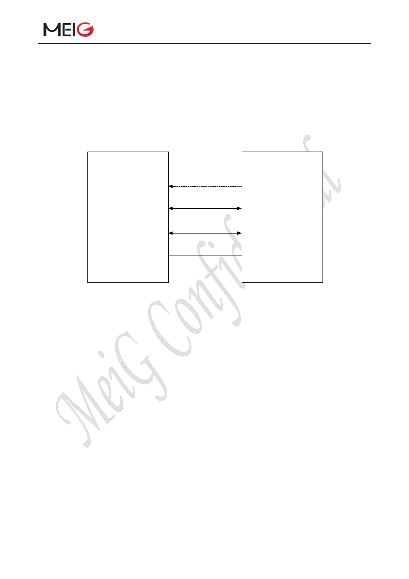
MeiGProductManualofSLM750Module
SLM750ModuleHardwareDesign Page 31, total 84 pages
preconditions can let the module enter into sleep mode.
Execute AT+SLEEPEN=1 command to enable sleep mode.
Keep WAKEUP_IN to high level.
Host USB interface connecting to the module enters into suspend state.
Sending data to SLM750 from USB will wake up the module.
Connections between the module and the host are as follows:
Module
USB_ VB US
USB_ DP
USB_ DM
GND
Host
VDD
USB_ DP
USB_ DM
GND
Figure 3 Sleep mode application with USB remote waking-up function
3.5.1.2 USB Application (without USB Suspend function)
If host does not support suspend function, you should disconnect VCC with external control
circuit to let the module enter into the sleep mode:
Execute command AT+SLEEPEN=1 to enable the sleep mode.
Disconnect USB_VDD.
Restoring the USB_VDD power supply can wake up the module.
3.5.1.3 Hardware I/O control sleep mode
The WAKEUP_IN (Pin1) pin is the pin that triggers sleep in the module. When the sleep
function of the module is enabled, the pin is pulled down (initially at a high level), and the module
triggers the sleep process after detecting the descent edge of the pin. In the case of full release of
sleep locks, the module will smoothly enter the sleep state.
Whether the sleep function of the module is enabled can be checked by at+ sleepen? via the
AT query, when the query returns a result of 0 indicating the current state of sleep function is
forbidden and the sleep function is enabled by 1. Similarly, you can use the AT query at + sleepen=1,

MeiGProductManualofSLM750Module
SLM750ModuleHardwareDesign Page 32, total 84 pages
or at + sleepen=0 to enable or disable sleep function of the module. When the module sleep function
is disabled, the module sleep related pin will be invalid, USB PHY will not enter the low power
(LPM) when the USB bus is suspended.
When the module is in a sleep state (WAKEUP_IN pin pulls down to trigger module sleep),
the pin should be pulled up, and at the same time, WAKEUP_IN will produce a rising edge, the
module will trigger a wake-up after detecting break in the rising edge, after that, the WAKEUP_IN
will remain high, and the module keeps awake.
The module control signal level supports 1.8 V logic level.
3.5.2 Flight Mode
When the module enters into flight mode, the RF function will not work, and all AT commands
correlative with RF function will be inaccessible. You can use the following ways to let the module
enter into flight mode:
3.5.2.1 Hardware I/O interface controls flight mode
The W_DISABLE_N pin (PIN4) of SLM750 gives the module a low level signal. The module
enters into flight mode and RF sending and receiving unit stops working. Pull up PIN4 and the
module will enter into normal mode.
Module control signal level supports 1.8V logical level.
3.5.2.2 AT command controls flight mode
Send AT+CFUN=4 command to let the module enter into flight mode, and RF sending and
receiving unit stops working at the time. Send AT+CFUN=1 command to let the module enter into
normal mode again.
3.6 Power Supply
3.6.1 Power supply pins
SLM750 has four VBAT pins to connect to external power and can be divided into two power
fields:
MeiGProductManualofSLM750Module
SLM750ModuleHardwareDesign Page 33, total 84 pages
Two VBAT_RF pins are used to supply RF power.
Two VBAT_BB pins are used to supply Baseband power.
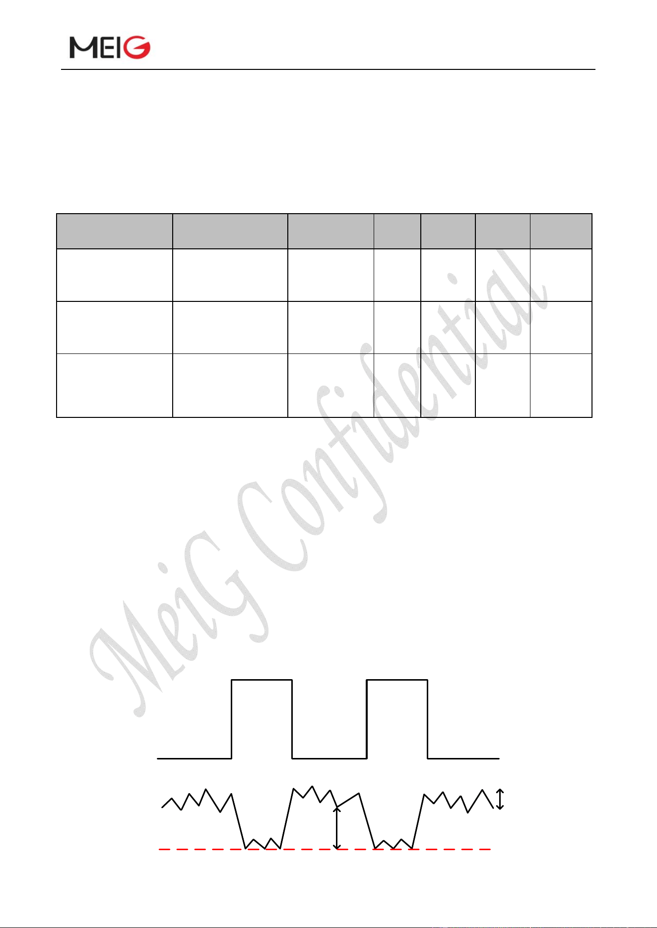
Below table shows the assignment of power and ground pins:
Table 7: Related power supply interfaces
Pin name Pin No. Description Min
value
Typical
value
Max
value
Unit
VBAT_BB 59,60 Power supply
for module
baseband
3.3 3.8 4.2 V
VBAT_RF 57,58 Power supply
for module
RF
3.3 3.8 4.2 V
GND
8,9,19,
22,36,46,48,50~54,
56,72,
85~112
Ground - 0 - V
3.6.2 Decrease voltage drop
The power supply range of SLM750 is from 3.3V to 4.2V. During data transmission or
conversation, instantaneous high-power emission will form a peak current up to 2A, which will lead
to a large ripple of VBAT. If instantaneous voltage drop leads to too low VBAT power supply
voltage, the module will shut down. Make sure there are sufficient power supply capabilities and
the input voltage will never drop below 3.3V to make the module work well.
The following figure shows the voltage drop during transmitting burst in 2G network. The
voltage drop will be less in 3G and 4G networks.
VBAT
Min.3.3V
Drop
Ripple
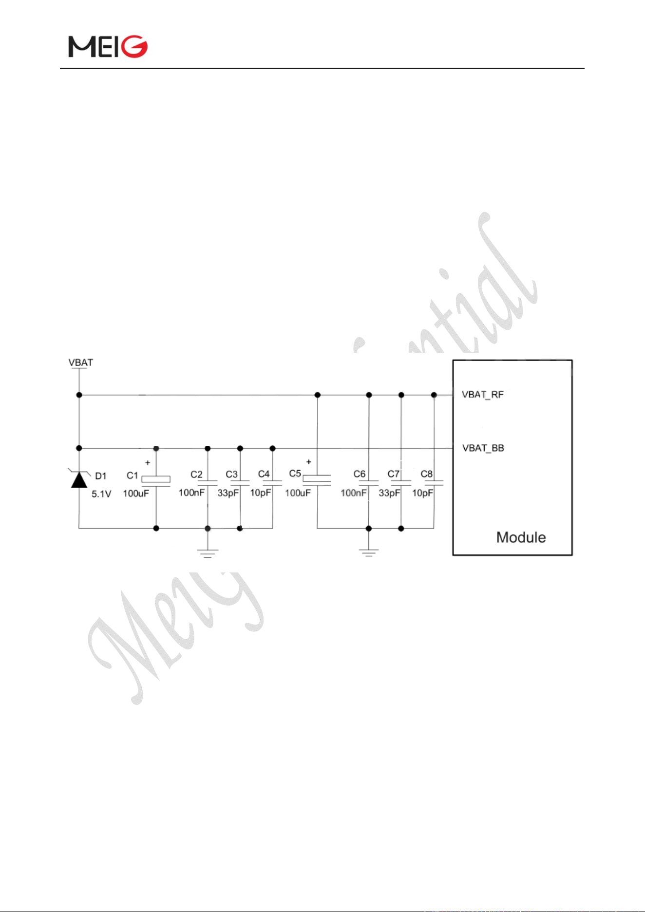
MeiGProductManualofSLM750Module
SLM750ModuleHardwareDesign Page 34, total 84 pages
Figure 4 Power requirements for burst transmission
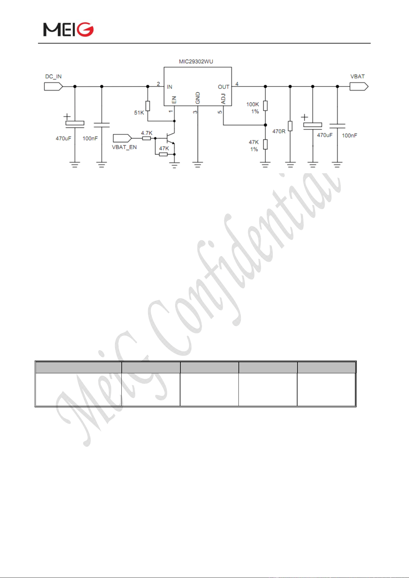
In order to reduce voltage drop, a low ESR 100uF filter capacitor is needed. The multilayer
ceramic capacitor (MLCC) has the best ESR, suggestion to add three ceramic capacitors (100nF,
33pF, 10pF) to VBAT_BB and VBAT_RF pins, and the capacitors should be placed close to the
VBAT pin. When external power supply makes connection to module, VBAT_BB and VBAT_RF
need to apply star line. VBAT_BB line width should not be less than 1 mm, and VBATRF line
width should not be less than 2 mm. In principle, the longer the VBAT line, the wider the line width.
In addition, in order to ensure the stability of the power supply, it is recommended to add a
Zener diode at the front end of the power supply with a power of 5.1V and a work and power of
0.5W or higher. The reference circuit is as follows:
Figure 5 Star structure of power supply
3.6.3 Reference design for power supply
The power design for the module is very important as the performance of the module largely
depends on the power supply. The power supply is capable of providing sufficient current up to 2A
at least. If the voltage drop between the input and output is not too high, it is recommended that you
use a LDO to supply power for the module. If there is a big voltage difference between the input
and the output, DCDC is preferred to be used as a power supply.
The following figure shows a reference design for +5V input power supply. The designed
output for the power supply is +3.3V (typical value 3.8V) and the maximum load current is 3A.
MeiGProductManualofSLM750Module
SLM750ModuleHardwareDesign Page 35, total 84 pages
Figure 6 DC power supply circuit
3.6.4 VDD_EXT voltage output
If SLM750 module turns on normally, there is a voltage output of 1.8V, current load 80mA in
PIN7. You can use the output voltage as external power supply, for example level reference, and
judge if the module is turned on by reading pin level status.
3.7 Turn On and Off
3.7.1 Turn on module using the PWRKEY
Table 7.1: Description of PWR_KEY pin
Pin name Pin number Function DC features Description
PWR_KEY 21 Turn on/off the
module
V
IH
max=2.1V
V
IH
min=1.3V
V
IL
max=0.5V
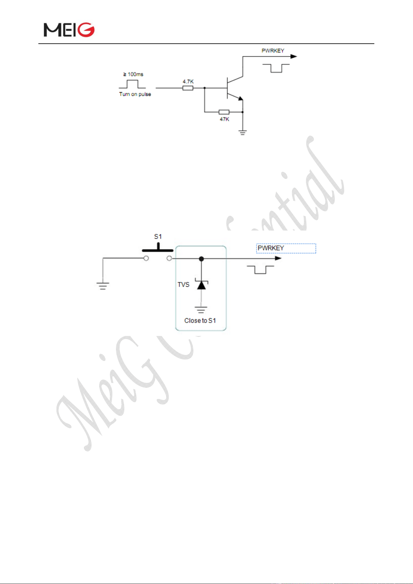
When SLM750 is in power down mode, it can be turned on to normal mode by driving the
PWRKEY pin to a low level for at least 100ms. It is suggested that you use an open set driver
circuit to control PWRKEY pin. After STATUS pin (require external pull-up) outputting a low level,
PWRKEY pin can be released. Reference circuit is illustrated in the following figure:
MeiGProductManualofSLM750Module
SLM750ModuleHardwareDesign Page 36, total 84 pages
Figure 7 Turn on the module using driving circuit
The other way to control the PWRKEY is using a button directly. A TVS component is
indispensable to be placed nearby the button for ESD protection. A reference circuit is shown in the
following figure:
Figure 8 Turn on the module using keystroke
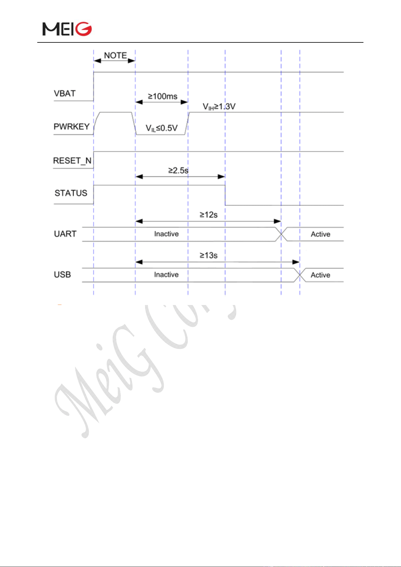
Turning on time is illustrated as follows:
MeiGProductManualofSLM750Module
SLM750ModuleHardwareDesign Page 37, total 84 pages
Figure 9 Timing of turning on module
Note:
1. Tnote > 30ms.
2. If the external pull up design of PWRKEY pin is added, it is recommended that the pull-up
level range is 1.3V~2.1V
3.7.2 Turn off module using the PWRKEY pin
Modules can be shut down in the following ways:
normal shutdown: shutdown through PWRKEY pin control module;
normal shutdown: shutdown through AT command
3.7.2.1 PWRKEY pin shutdown
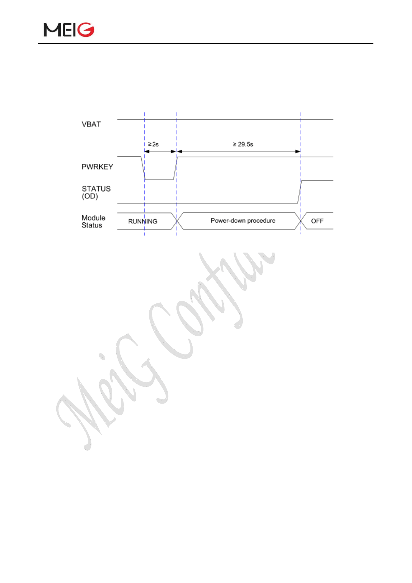
When the module is on, the PWRKEY pin is pulled down and released after holding at least 2s,
MeiGProductManualofSLM750Module
SLM750ModuleHardwareDesign Page 38, total 84 pages
then the module will perform the shutdown process. The shutdown sequence is shown in the
following figure:
Figure 10 Timing of turning off module
3.7.2.2 AT command shutdown
The AT + Poweroff command can be used to control the shutdown of module. This shutdown
process is equivalent to a pulled-down PWRKEY pin shutdown process.
NOTES: 1. When the module works properly, do not immediately cut off the module power to
avoid damage to the module internal Flash data. It is strongly recommended to turn off the module
by using the PWRKEY or AT command before disconnecting the power.
2. When using the AT command to shut down, make sure that the PWRKEY is always in a
high level state after the shutdown command execution, otherwise the module will automatically
boot again after shutdown.
3.8 Reset the Module
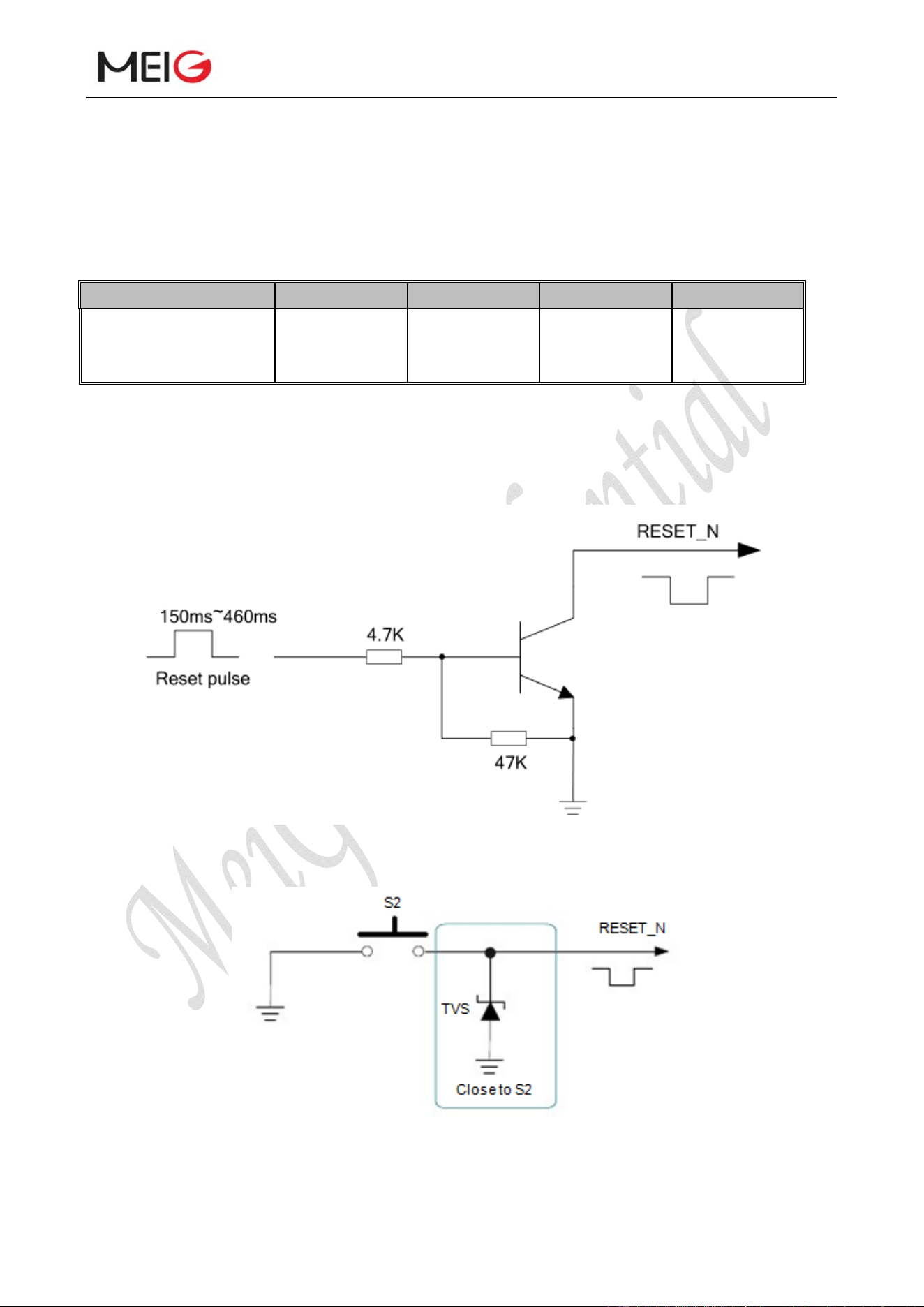
Hardware and AT command can be used to reset SLM750.
MeiGProductManualofSLM750Module
SLM750ModuleHardwareDesign Page 39, total 84 pages
3.8.1 Hardware reset
When the module is in operation, puling down 150~460ms of the RESET_N pin to reset
module. The RESET_N signal is sensitive to interference.
Table 8: RESET_N pin description
Pin name Pin number Function DC features Description
RESET_N 20 Reset module V
IH
max=2.1V
V
IH
min=1.3V
V
IL
max=0.5V
Reference circuit is as follows: you can use open set driver circuit or button to control
RESET_N pin.
Figure 11 Reference circuit of RESET_N by using driving circuit
Figure 12 Reference circuit of RESET_N by using button
The reset timing figure is as follows:
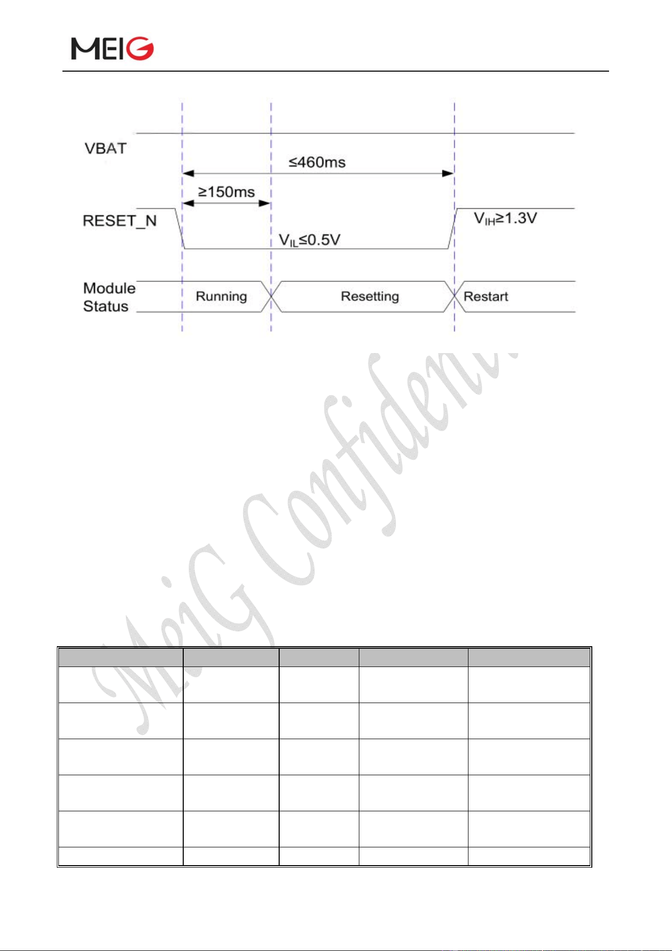
MeiGProductManualofSLM750Module
SLM750ModuleHardwareDesign Page 40, total 84 pages
Figure 13Reset timing of RESET_N
3.8.2 AT command reset
Enter AT+RESET command in SLM750VUART or USB AT interface to reset and restart
SLM750.
3.9 USIM/SIM Card Interface
USIM card interface meets ETSI and IMT-2000 SIM interface requirements. Both 1.8V and
3.0V USIM cards are supported by SLM750
Table 9: USIM/SIM card interface description
Pin name Pin number I/O Description Note
USIM_DATA 15 IO USIM card data
signal
USIM_CLK 16 DO USIM card clock
signal
USIM_RST 17 DO USIM card reset
signal
USIM_VDD 14 PO USIM card
power supply
Support 1.8V and
3.0V USIM card
USIM_PRESENCE 13 DI USIM card plug
detection
Require to pull up
to1.8V
GND 10 -
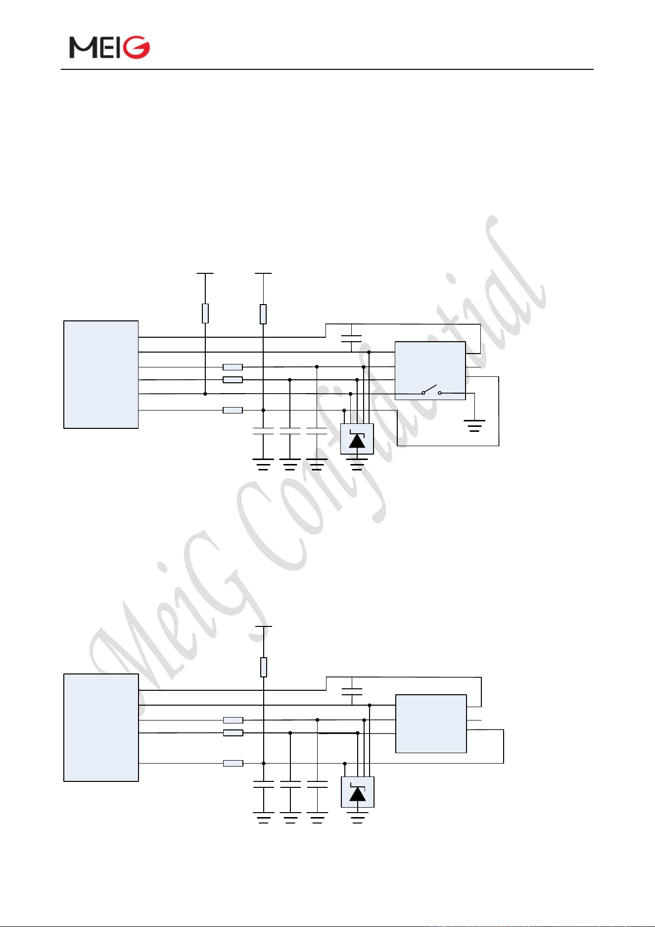
MeiGProductManualofSLM750Module
SLM750ModuleHardwareDesign Page 41, total 84 pages
SLM750 supports USIM card hot plugging and hot plugging function is turned off by default.
The following figure shows USIM_PRESENCE pin high level, no card, USIM_PRESENCE pin
ground after inserting card on SIM card connector.
SLM750 supports USIM hot plugging function through the USIM_PRESENCE pin, support
high-level detection, and the default hot-plugging function is turned off by default. The
USIM_PRESENCE pin level is in high voltage after the SIM card is inserted as shown in below
figure, The USIM_PRESENCE pin level is in low voltage when no card is detected.
Module
USIM_GND
USIM_VDD
USIM_RST
USIM_CLK
USIM_PRESENCE
USIM_DATA
VCC
RST
CLK
GND
VPP
IO
22R
22R
22R
GND
33PF 33PF 33PF
100nF
51K 15K
VDD_EXT USIM_VDD
USIM CARD CONNECTOR
Figure 14 Reference circuit for 8-pin USIM/SIM connector
If USIM card detection function is not required, keep USIM_PRESENCE pin pulling up to
1.8V. The following figure is a reference circuit for 6-pin USIM/SIM connector:
Module
USIM_GND
USIM_VDD
USIM_RST
USIM_CLK
USIM_DATA
VCC
RST
CLK
GND
VPP
IO
22R
22R
22R
33PF 33PF 33PF
100nF
15K
USIM_VDD
USIM CARD C ONNECTOR
Figure 15 Reference circuit for 6-pin USIM/SIM connector

MeiGProductManualofSLM750Module
SLM750ModuleHardwareDesign Page 42, total 84 pages
In order to enhance the reliability and availability of the USIM card in your application, please
follow the criteria below in the USIM circuit design:
USIM_DATA requires a pull-up resistor of 15kΩ to USIM_VCC; the pull-up resistor helps to
increase SIM card's anti-interference ability. When USIM card trace is too long or it is close to
the interference source, it is recommended that you add a pull-up resistor near the card.
In order to suppress stray EMI and enhance ESD protection, it is recommended to connect a
resistance of 22Ω on USIM_DATA, USIM_CLK and USIM_RST line.
In order to improve the antistatic ability and offer good ESD protection, it is recommended to
add TVS whose parasitic capacitance should be less than 15pF on USIM_VDD, USIM_DATA,
USIM_CLK and USIM_RST line.
In order to filter GSM900 interference, add a parallel 33pF resistance on USIM_VDD,
USIM_DATA, USIM_CLK and USIM_RST line.
Keep layout of USIM card as close as possible to the module. Assure the length of signal
wiring is less than 200mm.
Keep USIM card signal away from RF and VBAT power line.
To avoid cross-talk between USIM_CLK and USIM_DATA, keep them away from each other
and shield them with surrounded ground.
Complete hot plugging of USIM/SIM card by using the DETECT pin of hot plug card slot and
the 13pin of the module. The default setting does not support hot plug function. Contact us if
you need more information about the function.
Note: Hot plug of SIM Connectors is not supported. Hot plug to USIM and SIM card can
cause damages to USIM /SIM card or SLM750V USIM /SIM card interfaces.
3.10 USB Interface
SLM750 provides a USB interface which complies with USB 2.0 specification and supports
high-speed (480Mbps) and full-speed (12Mbps) modes. The USB interface is used for AT command
communication, data transmission, software debugging and version upgrade.
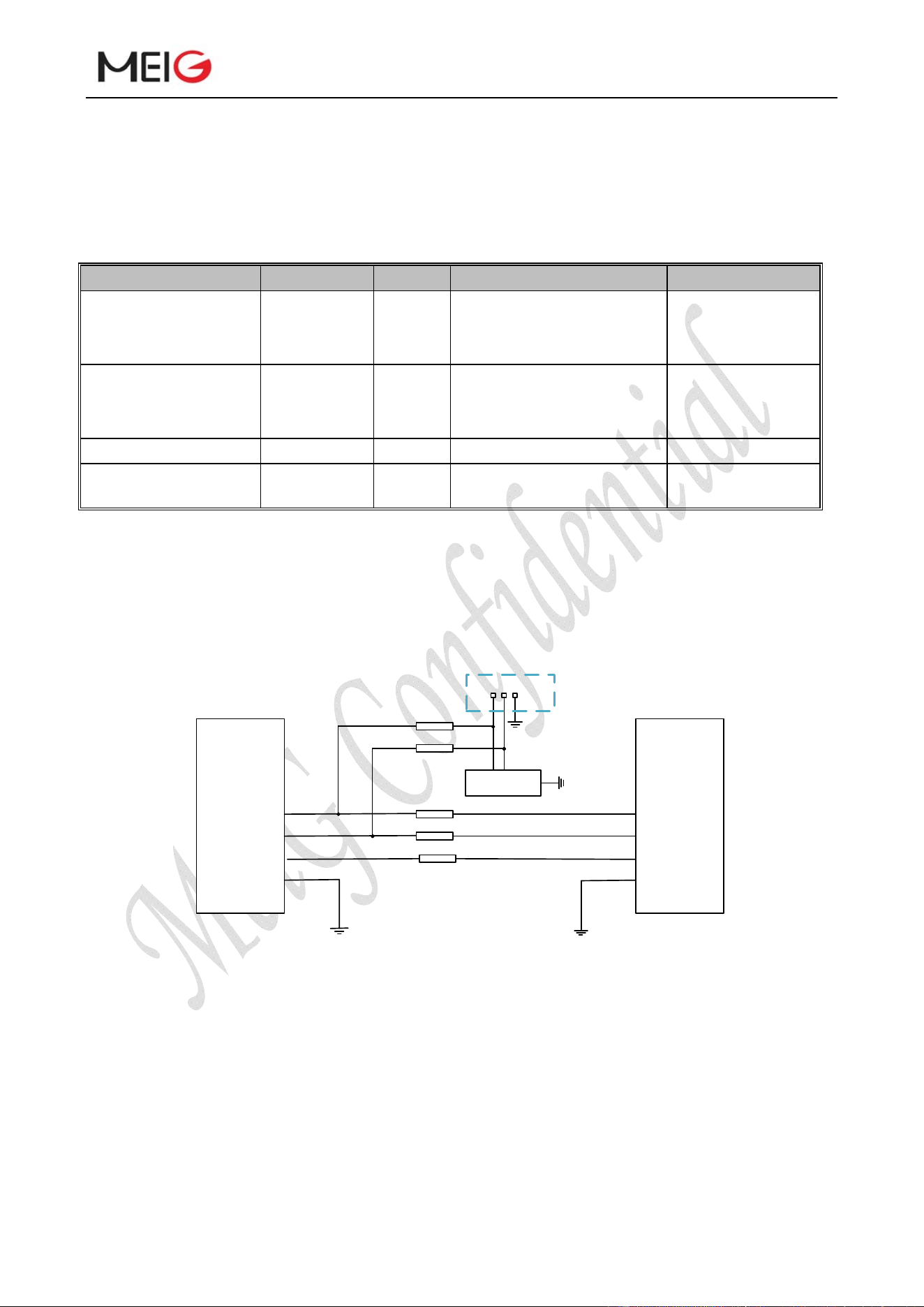
MeiGProductManualofSLM750Module
SLM750ModuleHardwareDesign Page 43, total 84 pages
3.10.1 USB pin description
SLM750 module provides a USB2.0 High-Speed interface.
Table 10: USB interface description
Name Pin name I/O Description Note
USB_DM 70 IO USB differential data
signal-
Require 90Ω
differential
impedance
USB_DP 69 IO USB differential data
signal+
Require 90Ω
differential
impedance
GND 72 - Ground
USB_VBUS
71 PI
USB power supply, used
for USB detection
Typical value
5.0V
3.10.2 USB reference circuit
USB interface application reference circuit of SLM750 is shown in the following figure.
USB_DM
ESD Array
Test Points
R2 0R
R1 0R
R4
R3
NM 0R
NM 0R
USB_DP
GND
USB_DM
USB_DP
GND
Module MCU
R5
0R
USB_VBUS
USB_VBUS
Figure 16 USB reference circuit
In order to meet the signal integrity requirements of the USB data line, the resistors R1/ R2/
R3/ R4 must be placed close to the module, and the resistors need to be placed close to each other.
The connection point branch must be as short as possible.
In the design of USB interface circuit, in order to ensure the performance of USB, the
following principles are recommended in circuit design:

MeiGProductManualofSLM750Module
SLM750ModuleHardwareDesign Page 44, total 84 pages
The module USB_VBUS is not used to power the module, but is used to detect the insertion
and pull-out of the USB.
In order to reduce the signal interference of USB high speed data transmission, connect R1 and
R2 between USB_DM and USB_DP interface circuit to improve the data transmission rate. It is
recommended that you use R1 and R2 of 0Ω.
In order to improve the antistatic performance of USB interface, it is recommended to add ESD
protection components on USB_DP and USB_DM interface circuit. It is recommended that you
use ESD components with junction capacitance less than 2pF.
In order to ensure that the USB is reliable, consider more about the protection of USB when
designing, such as the protection of USB on Layout requires impedance control of 90Ω for
USB_DP, USB_DM, tracing strictly according to differential requirements, and keeping away
from the interference signal as far as possible.
Do not trace the USB line in the crystal oscillator, oscillator, magnetic device and RF signal; it
is recommended to trace inner differential line and up and down around the package.
3.10.3 USB driver
SLM750 supports various operation systems, such as PC operation systems: Windows 10,
Windows 7/8,embedded operation system, Linux2.6 or higher, Android
2.3/4.0/4.2/4.4/5.0/5.1/6.0/7.0, which requires private USB driver support.
For different operating systems and different VID and PID, USB driver provides different
driver files. Contact supporting staff if you have specific requirements.
3.11 UART Interface
SLM750 provides two UART interfaces: main UART interface and debug UART interface.
The features of them are illustrated as below:
Main UART interface supports 9600, 19200, 38400, 57600, 115200, 230400, 460800,
921600bps and 30000000bps baud rate, the default is 115200bps. The interface can be used
for data transmission and AT command communication.
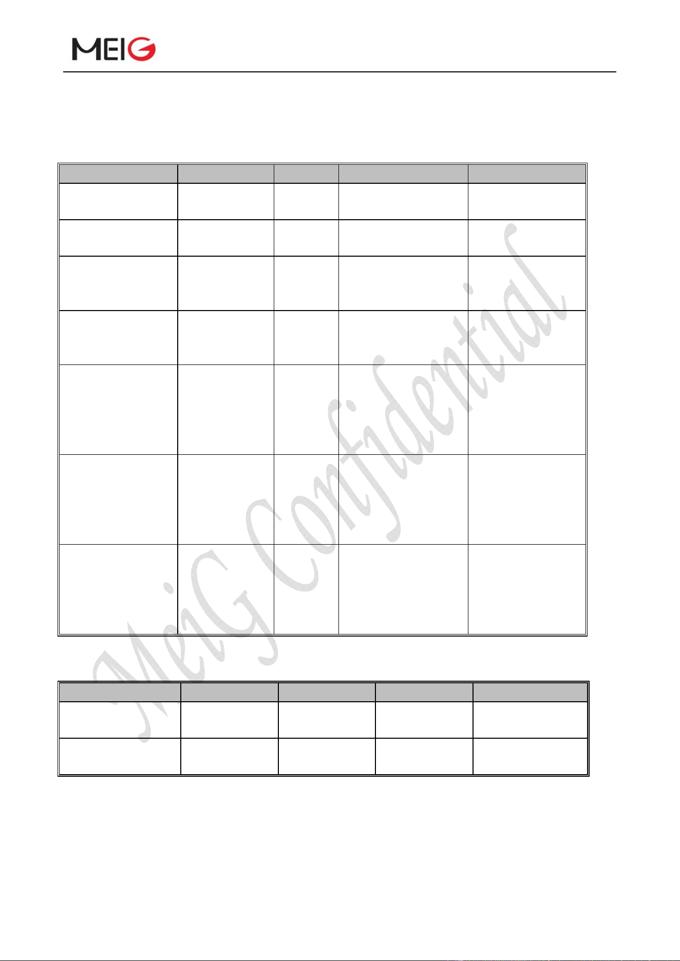
MeiGProductManualofSLM750Module
SLM750ModuleHardwareDesign Page 45, total 84 pages
Debug UART interface supports 115200bps baud rate. It can be used for Linux console, log
print.
Table 11: Main UART pin description
Pin name Pin number I/O Description Note
RXD 68 DI Receive data 1.8V power
domain
TXD 67 DO Transmit data 1.8V power
domain
CTS 64 DI Clear to send 1.8V power
domain. If unused,
keep it open
RTS 65 DO DTE requires to
transmit data
1.8V power
domain. If unused,
keep it open
RI 62 DO Ring indicator 1.8V power
domain. If unused,
keep it open. The
function is to be
development.
DCD 63 DO Output carrier detect 1.8V power
domain. If unused,
keep it open. The
function is to be
development.
DTR 66 DI DTE ready, sleep
mode control
1.8V power
domain. If unused,
keep it open. The
function is to be
development.
Table 12: Debug UART pin description
Pin name Pin number I/O Description Note
DBG_RXD 11 DI Receive data 1.8V power
supply domain
DBG_TXD 12 DO Transmit data 1.8V power
supply domain
Table 13: UART logical level
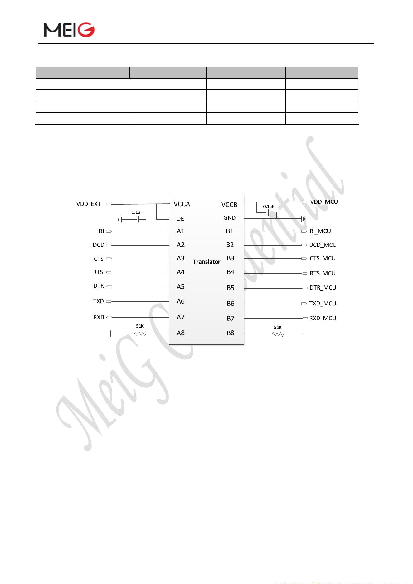
MeiGProductManualofSLM750Module
SLM750ModuleHardwareDesign Page 46, total 84 pages
Parameter Min Max Unit
V
IL
-0.3 0.6 V
V
IH
1.2 2.0 V
V
OL
0 0.45 V
V
OH
1.35 1.8 V
SLM750 provides 1.8V serial port. If your application serial port is 3.3V, you need to add level
converter. It is recommended that you use TXB0104PWR from TI Company. Reference design is
shown as follows:
Figure 17 Reference circuit of level conversion chip
3.12 PCM and I2C Interface
SLM750 provides one PCM interface which supports the following two modes:
Short frame mode: the module works as both master and slave
Long frame mode: the module works as master only
In short frame mode, the data is sampled on the falling edge of the PCM_CLK and transmitted
on the rising edge; the PCM_SYNC falling edge represents the more significant bit. PCM_CLK
supports 128, 256, 512, 1024 and 2048kHz speech codes.
In long frame mode, the data is sampled on the falling edge of the PCM_CLK and transmitted
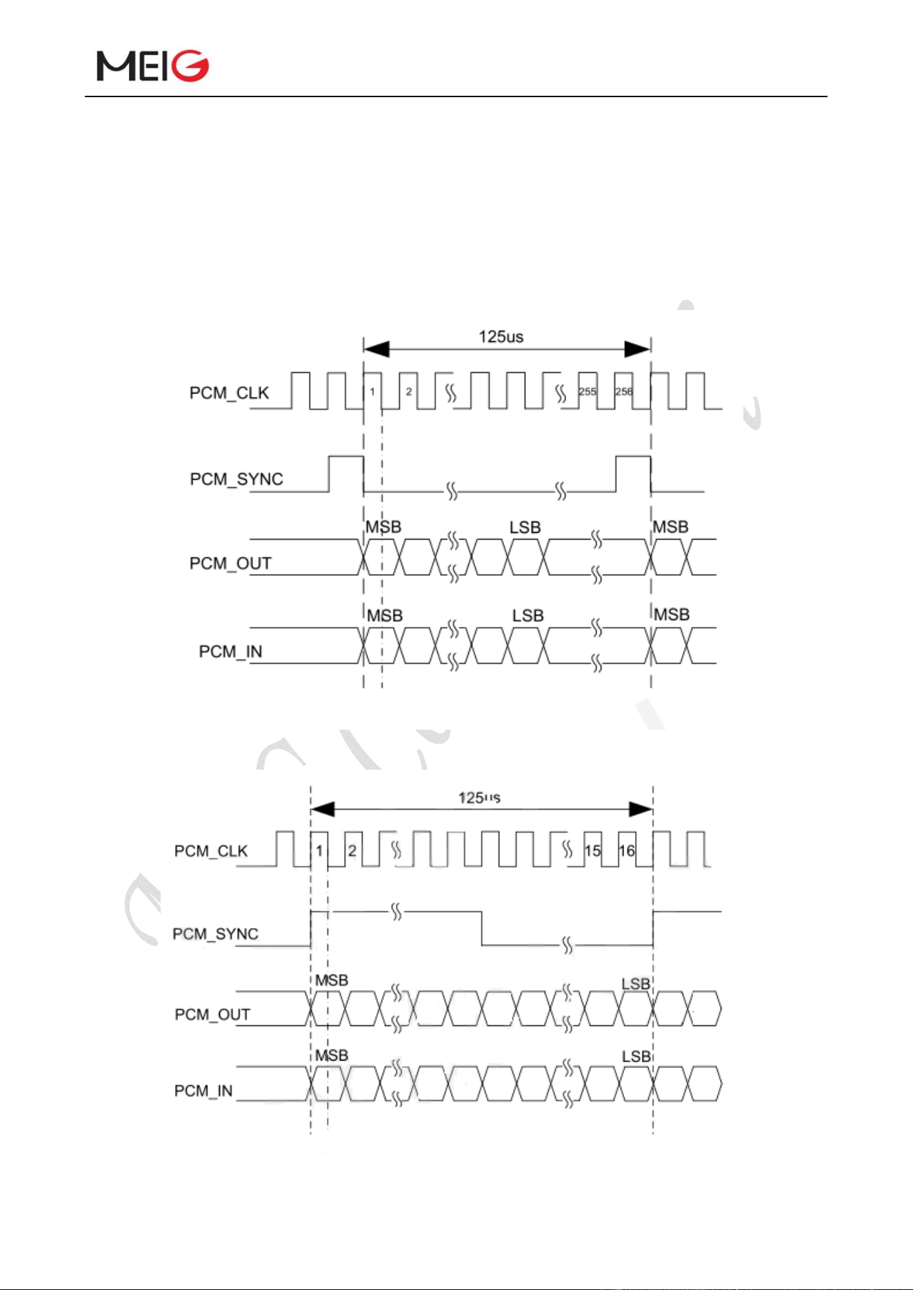
MeiGProductManualofSLM750Module
SLM750ModuleHardwareDesign Page 47, total 84 pages
on the rising edge; the PCM_SYNC rising edge represents the more significant bit. The mode only
supports 128 kHz PCM_CLK and 8kHz, 50% duty cycle PCM_SYNC.
SLM750 supports 8-bit A-law, u-law and 16-bit linear encoding formats. The following figures
show the timing relationship in short frame mode with PCM_SYNC=8 kHz and
PCM_CLK=2048kHz, as well as the timing relationship in long frame mode with PCM_SYNC=8
kHz and PCM_CLK=128kHz.
Figure 18 Timing in short frame mode
Figure 19 Timing in long frame mode
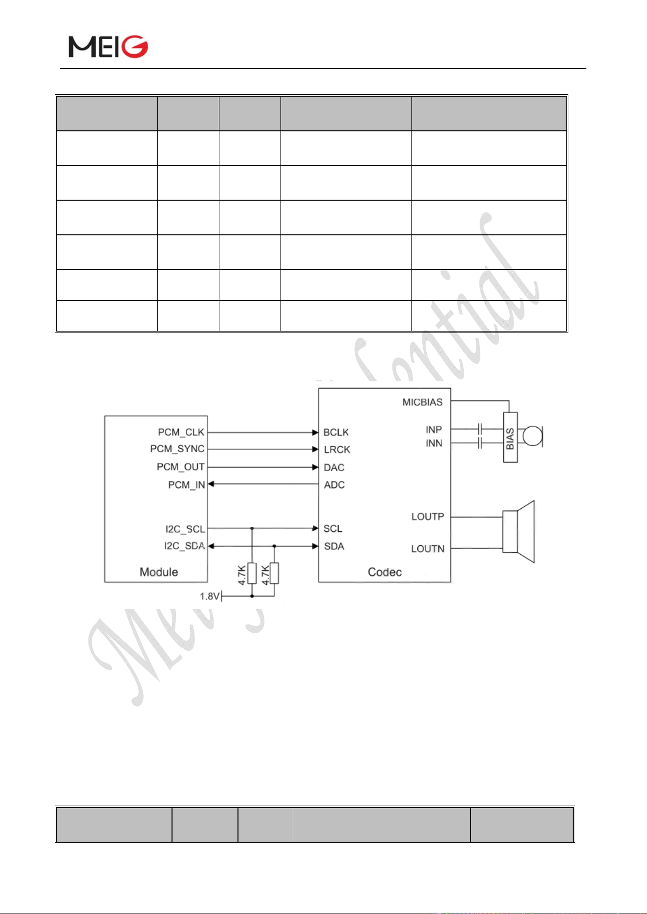
MeiGProductManualofSLM750Module
SLM750ModuleHardwareDesign Page 48, total 84 pages
Table 14: Pin description for PCM interface
Pin name Pin
number
I/O Description Note
PCM_CLK 27 IO PCM clock 1.8V power supply
domain
PCM_OUT 25 DO PCM data output 1.8V power supply
domain
PCM_IN 24 DI PCM data input 1.8V power supply
domain
PCM_SYNC 26 IO PCM data
synchronous signal
1.8V power supply
domain
I2C_SCL 41 OD I2C clock
Require 1.8V external
pulling-up
I2C_SDA 42 OD I2C data
Require 1.8V external
pulling-up
The following figure shows a reference design of PCM interface with an external codec IC.
Figure 20 Reference design for PCM circuit
3.13 Network Status Indication
The network indication pins can be used to drive a network status indicator LED. SLM750
provides two network indication pins: NET_MODE and NET_STATUS. The following tables
describe pin definition and logic level changes in different network status.
Table 15: Pin Definition of Network Indicator
Pin name Pin
number
I/O Description Note
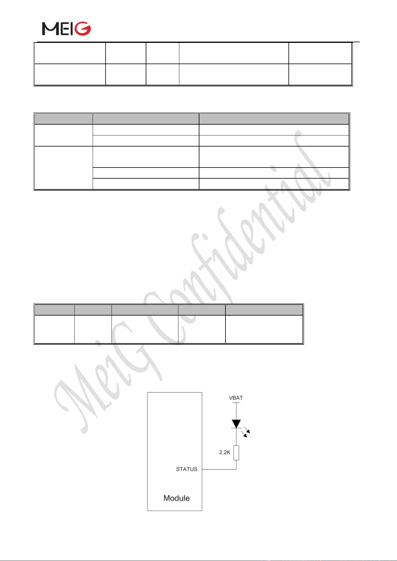
MeiGProductManualofSLM750Module
SLM750ModuleHardwareDesign Page 49, total 84 pages
NET_STATUS 6 DO Indicate the module network
activity status.
1.8V power
supply domain
NET_MODE 5 DO Indicate the module network
registration mode.
1.8V power
supply domain
Table 16: Working State of the Network Indicator
Mode Status Description
NET_MODE High level
Register LTE network status
Low level Others
NET_ STATUS Flicker (200ms OFF/1400ms
ON)
Data transfer status
High level Registration success
Low level Others
3.14 Status
The STATUS pin is an open drain output for indicating the module’s operation status. You can
connect it to a GPIO of DTE with a pull up resistor, or as the LED indication circuit shown below.
When the module is turned on normally, the STATUS will present high level.
Table 17: STATUS pin description
Pin name Pin no. Description I/O Note
STATUS 61
Indicate the
module operation
status
OD
Require external
pulling-up
The following figure shows different design circuits of STATUS, you can choose either one
according to your application demands.
MeiGProductManualofSLM750Module
SLM750ModuleHardwareDesign Page 50, total 84 pages
Figure 21 Reference circuit of STATUS
3.15 ADC Function
SLM750 provides two analogy- to-digital converters. Using AT+ADCREAD=1 to read the
voltage value of ADC0. Using AT+ADCREAD=6 read the voltage value of ADC1.
Table 18: ADC pin description
Pin name Pin no. Description
Voltage range Resolution
ADC0 45 Analogy to digital
converter interface 0
0.05 – 1.8V 15bits
ADC1 44 Analogy to digital
converter interface 1
0.05 – 1.8V 15bits
NOTES: 1. The ADC interface cannot directly connect to any input voltage when the module is
not powered by VBAT.
2. It is recommended that the ADC pin adopt the input of the voltage divider circuit.
3.16 SGMII Interface
SLM750 includes an integrated Ethernet MAC with an SGMII interface and two management
interfaces(MDIO), key features of the SGMII interface are shown below:
IEEE802.3 compliance
Full duplex at 1000Mbps
Half/full duplex for 10/100Mbps
Support VLAN tagging
Support IEEE1588 and Precision Time Protocol (PTP)
Can be used to connect to external Ethernet PHY like AR8033, or to an external switch
MDIO supports dual voltage 1.8V/2.85V
Pin definitions of SGMII interface are as bellow:
Table 19: Pin definition of SGMII interface
Pin name Pin no. I/O Description Comment
EPHY_RST_N 119 DO Ethernet PHY
reset
1.8V /2.85V power domain.
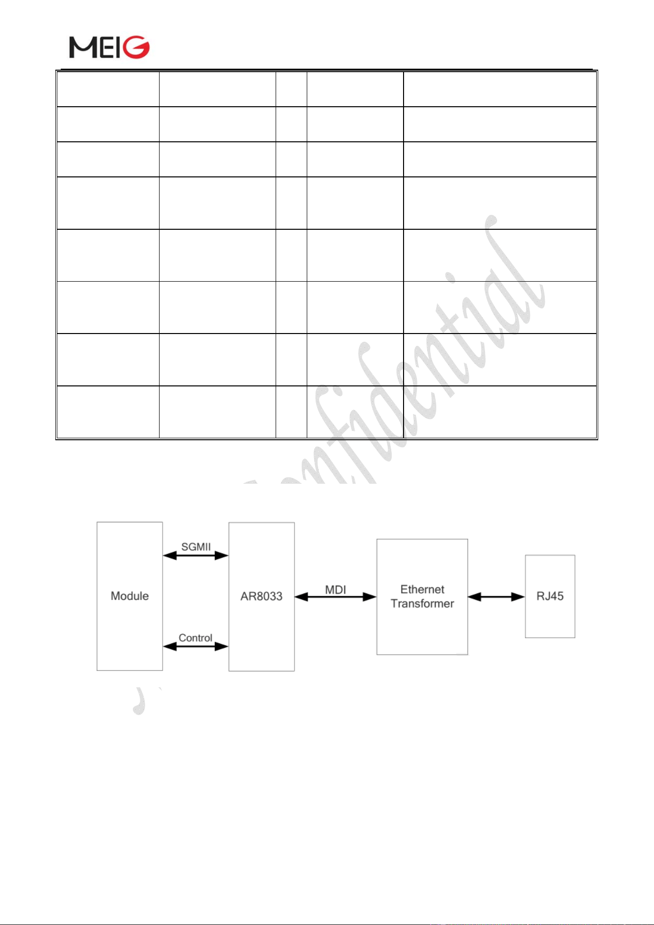
MeiGProductManualofSLM750Module
SLM750ModuleHardwareDesign Page 51, total 84 pages
EPHY_INT_N 120 DI Ethernet PHY
interruption
1.8V /2.85V power domain.
SGMII_MDATA 121 IO SGMII MDIO
data
1.8V/2.85V power domain.
SGMII_MCLK 122 DO SGMII MDIO
clock
USIM2_VDD 128 PO SGMII MDIO
power supply
1.8V/2.85V power domain,
require external pull-up level for
SGMII SDIO Pin
SGMII_TX_M 123 AO SGMII data
transmit
negative signals
Connect with a 0.1uF capacitor,
close to the PHY side.
SGMII_TX_P 124 AO SGMII data
transmit
positive signals
Connect with a 0.1uF capacitor,
close to the PHY side.
SGMII_RX_P 125 AI SGMII data
receive positive
signals
Connect with a 0.1uF capacitor,
close to the PHY side.
SGMII_RX_M 126 AI SGMII data
receive
negative signals
Connect with a 0.1uF capacitor,
close to the PHY side.
The following figure shows the simplified block diagram for Ethernet application.
Figure 22 Simplified Block Diagram for Ethernet Application
The following figure shows a reference design of SGMII interface with PHY AR8033
application.
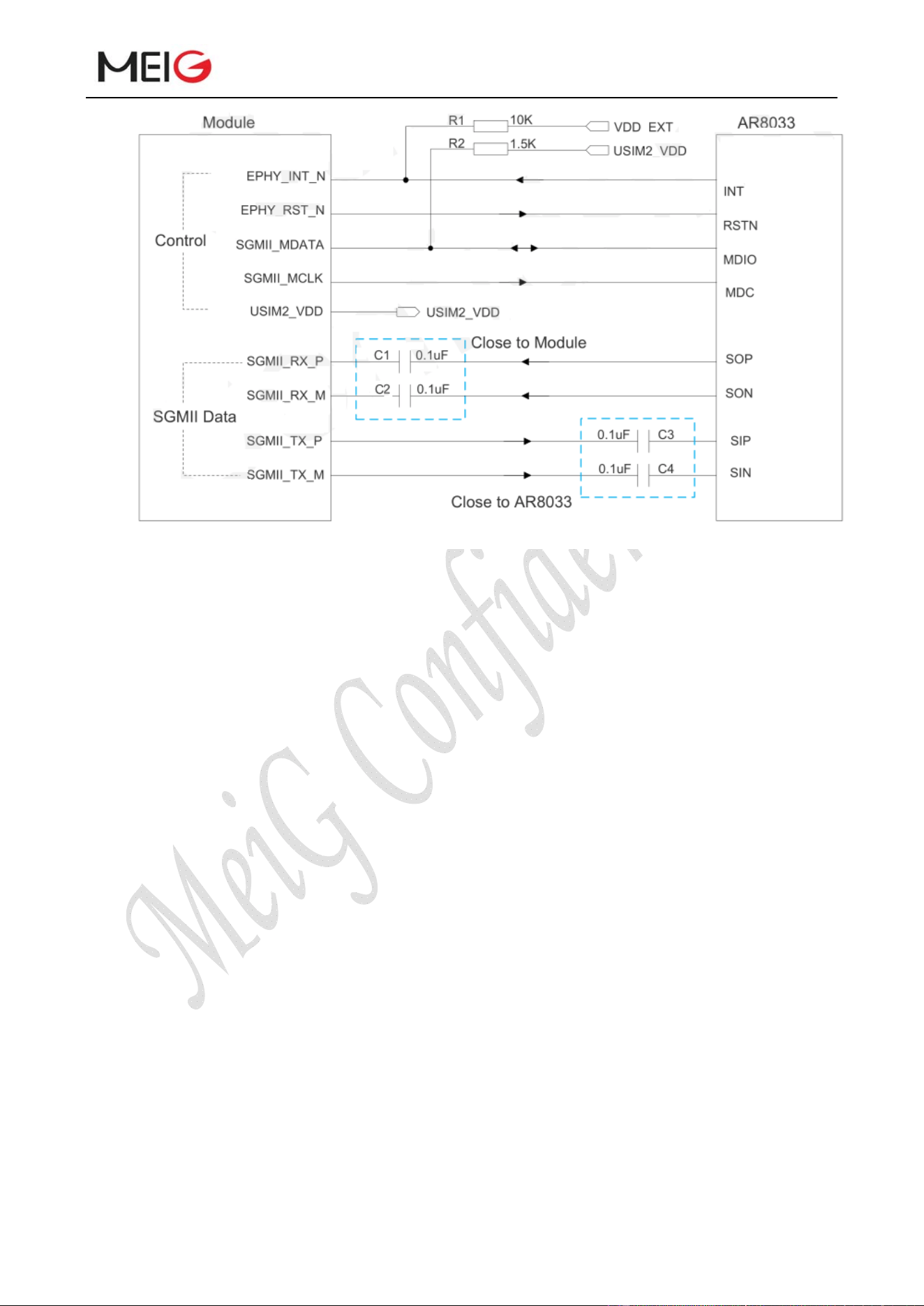
MeiGProductManualofSLM750Module
SLM750ModuleHardwareDesign Page 52, total 84 pages
Figure 23 Reference Circuit of SGMII Interface with PHY AR8033 Application
In order to enhance the reliability and availability in your application, please follow the criteria
below in the Ethernet PHY circuit design:
Keep SGMII data and control signals away from RF and VBAT trace.
Keep the maximum trace length less than 25.4cm and keep skew on the differential pairs less
than 0.7mm.
The differential impedance of SGMII data trace is 100 ohm±10%.
SGMII RX/TX line spacing is at least 3 times width, SGMII signal distance from other signal
lines is to maintain at least 3 times line width.
SGMII RX modules already have 0.1uf capacitors and do not need to be added externally
3.17 Wireless Connectivity Interfaces
SLM750 supports a low-power SDIO 3.0 interface for WLAN and a PCM interface for BT.
The following table shows the pin definition of wireless connectivity interfaces.
Table 20: Pin Definition of Wireless Connectivity Interfaces
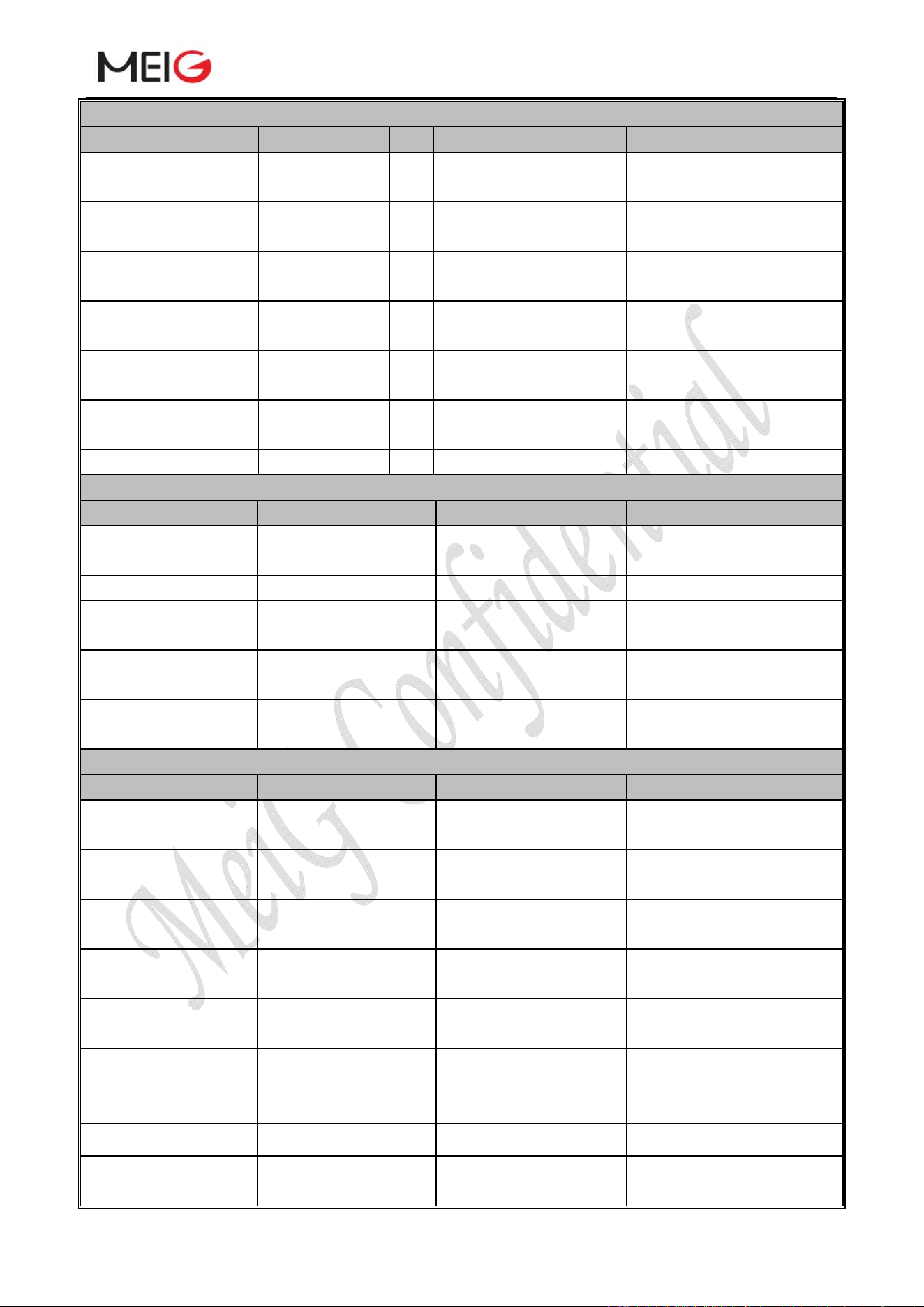
MeiGProductManualofSLM750Module
SLM750ModuleHardwareDesign Page 53, total 84 pages
WLAN part
Pin name Pin number I/O Description Note
SDC1_DATA3 129 IO WLAN SDIO signal
data line 3
1.8V power domain.
SDC1_DATA2 130 IO WLAN SDIO signal
data line 2
1.8V power domain.
SDC1_DATA1 131 IO WLAN SDIO signal
data line 1
1.8V power domain.
SDC1_DATA0 132 IO WLAN SDIO signal
data line 0
1.8V power domain.
SDC1_CLK 133 DO WLAN SDIO signal
clock
1.8V power domain.
SDC1_CMD 134 IO WLAN SDIO
instruction signal
1.8V power domain.
WLAN_EN 136 DO WLAN enables 1.8V power domain.
Coexistence and control part
Pin name Pin number I/O Description Note
PM_ENABLE 127 DO External 3.3V power
control
1.8V power domain.
WLAN_SLP_CLK 118 DO WLAN sleep clock Output 32kHz clock
WAKE_ON_WIREL
ESS*
135 DI WLAN wakes up the
module
1.8V power domain,
pending development
COEX_UART_RX 137 DI LTE/WLAN&BT
coexistence signal
1.8V power domain.
COEX_UART_TX 138 DO LTE/WLAN&BT
coexistence signal
1.8V power domain.
BT part
Pin name Pin number I/O Description Note
BT_EN 139 DO Bluetooth
enables.
1.8V power domain.
Active high level.
BT_RTS* 37 DO Request sending data 1.8V power domain,
suspend it when unused
BT_TXD* 38 DO Bluetooth
sends data
1.8V power domain.
BT_RXD* 39 DI Bluetooth receives
data
1.8V power domain.
BT_CTS* 40 DI Bluetooth sending
clearance
1.8V power domain.
PCM_IN 24 DI PCM data
input
1.8V power domain.
PCM_OUT 25 PCM data output 1.8V power domain.
PCM_CLK 27 IO PCM clock. 1.8V power domain.
PCM_SYNC 26 IO PCM data
synchronous
1.8V power domain.
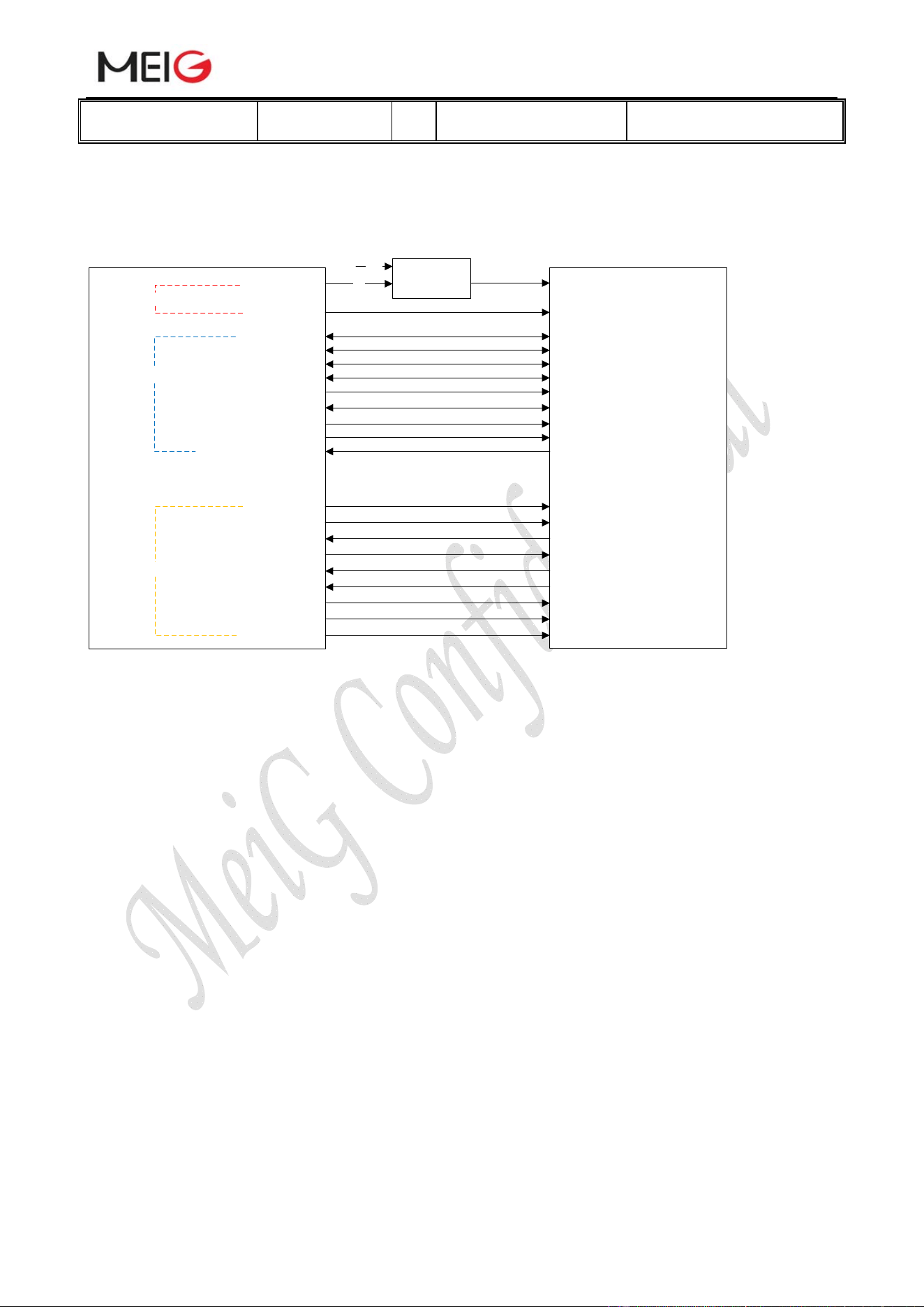
MeiGProductManualofSLM750Module
SLM750ModuleHardwareDesign Page 54, total 84 pages
signal.
The following figure shows a reference design of Wireless Connectivity interfaces with
SLM158 module.
Module SLM158Module
DCDC/LDO
EN
PM_EMBLE
VDD_EXT
SDC1_DATA3
SDC1_DATA1
SDC1_DATA0
SDC1_DATA2
SDC1_CLK
SDC1_CMD
WLAN_EN
WLAN_SLP_CLK
WAKE_ON_WIRELESS
BT_EN
BT_UART_RTS
BT_UART_CTS
BT_UART_TXD
BT_UART_RXD
PCM_IN
PCM_OUT
PCM_SYNC
VDD_3V3
VIO
VCC
PCM_CLK
SDC1_DATA3
SDC1_DATA1
SDC1_DATA0
SDC1_DATA2
SDC1_CLK
SDC1_CMD
WLAN_EN
WLAN_SLP_CLK
WAKE_ON_WIRELESS
BT_EN
BT_UART_CTS
BT_UART_RTS
BT_UART_RXD
BT_UART_TXD
PCM_OUT
PCM_IN
PCM_SYNC
PCM_CLK
POWER
WLAN
Bluetooh
Figure 24 Reference Circuit of Wireless Connectivity Interfaces with SLM158
Note:
1. SLM158 can only be used as slave equipment.
2. When SLM750 modules enable Bluetooth, PCM_SYNC and PCM_CLK are used only for
signal output.
3. The 24~27 pin is a multiplexed pin, which can be used for Codec voice or PCM connected
to SLM750V to realize Bluetooth voice communication.
4. *functionality is pending for development
3.17.1 WLAN Interface
SLM750 provides a low power SDIO 3.0 interface and control interface for WLAN design.
SDIO interface supports Single data rate mode, it maximum frequency is 50MHz.
As SDIO signals are very high-speed, in order to ensure the SDIO interface design corresponds
with the SDIO 3.0 specification, please comply with the following principles:
It is important to route the SDIO signal traces with total grounding. The impedance of SDIO
MeiGProductManualofSLM750Module
SLM750ModuleHardwareDesign Page 55, total 84 pages
signal trace is 50 ohm (±10%).
Protect other sensitive signals/circuits (RF, analog signals, etc.) from SDIO corruption and
protect SDIO signals from noisy signals (clocks, DCDCs, etc.).
It is recommended to keep matching length between CLK and DATA/CMD less than 1mm and
total routing length less than 50mm.
Keep termination resistors within 15~24 ohm on clock lines near the module and keep the route
distance from the module clock pins to termination resistors less than 5mm.
3.17.2 BT Interface
SLM750 supports UART and PCM interface for BT application. Further information about BT
interface will be added in future version of this document.
3.18 SD Card Interface
SLM750 provides a SD card interface which supports SD 3.0 protocol. The following tables
show the pin definition.
Table 21: Pin Definition of the SD Card Interface
Pin name Pin number I/O Description Note
SD_CMD 33 IO SD card SDIO
bus instruction
signal
SDIO signal level can be selected
according to the signal level
supported by SD card. Please
refer to SD3.0 protocol for
details. suspend it when no used
SD_CLK 32 DO SD card SDIO
bus clock
signal
SDIO signal level can be selected
according to the signal level
supported by SD card. Please
refer to SD3.0 protocol for
details. suspend it when no used
SD_DATA3 28 IO SD card SDIO
signal data line
3
SDIO signal level can be selected
according to the signal level
supported by SD card. Please
refer to SD3.0 protocol for
details. suspend it when no used
SD_DATA2 29 IO SD card SDIO
signal data line
2
SDIO signal level can be selected
according to the signal level
supported by SD card. Please
refer to SD3.0 protocol for
details. suspend it when no used
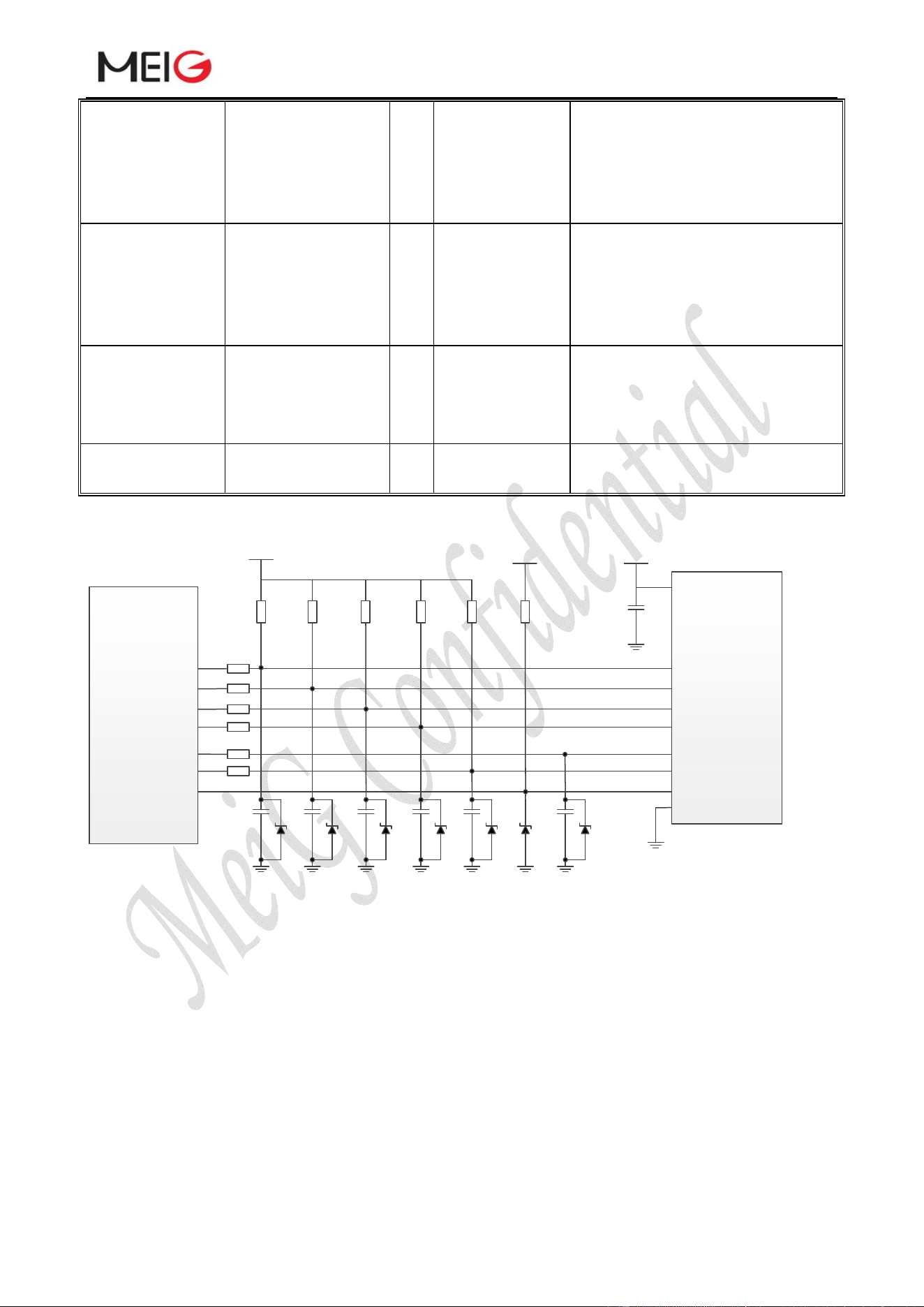
MeiGProductManualofSLM750Module
SLM750ModuleHardwareDesign Page 56, total 84 pages
SD_DATA1 30 IO SD card SDIO
signal data line
1
SDIO signal level can be selected
according to the signal level
supported by SD card. Please
refer to SD3.0 protocol for
details. suspend it when no used
SD_DATA0 130 IO SD card SDIO
signal data line
0
SDIO signal level can be selected
according to the signal level
supported by SD card. Please
refer to SD3.0 protocol for
details. suspend it when no used
VDD_SDIO 34 PO SD card SDIO
bus pulled up
power supply
The output 2.85V/1.8V is
configurable. Cannot be used for
SD card power supply, suspend it
when no used
SD_INS_DET 23 DI SD card insert
detection
1.8V power domain, suspend it
when unused
The following figure shows a reference design of SD card interface.
SD_DATA3
SD_DATA2
SD_DATA1
SD_DATA0
SD_CLK
SD_CMD
SD_INS_DET
R1 0R
R2 0R
R3 0R
R4 0R
R5 0R
R6 0R
C1
NM
D1
C2
NM
D2
C3
NM
D3
C4
NM
D4
C5
NM
D5
D7
C6
NM
D6
VDD
CD/DAT3
DAT2
DAT1
DAT0
CLK
CMD
DETECTIVE
VSS
VDD_3VVDD_EXT
VDD_3V
SD Card Connector
C7
100nF
R7
NM
R8
NM
R9
NM
R10
NM
R11
NM
R12
470K
Module
Figure 25 Reference Circuit of SD Card Application
In the circuit design of SD card interface, in order to ensure the good performance and
reliability of SD card, the following principles are recommended in circuit design:
The voltage range of SD card power supply VDD_3V is 2.7~3.6V and a sufficient current up to
0.8A should be provided. As the maximum output current of VDD_SDIO is 50mA which can
only be used for SDIO pull-up resistors, an externally power supply is needed for SD card.
To maximally limit the surge current caused by SD card insertion, the bypass capacitor (C7) of
SD card power source should not exceed 5uF.
To avoid jitter of bus, resistors R7~R11 are needed to pull up the SDIO to VDD_SDIO. Value
of these resistors is among 10~100kohm and the recommended value is 100kohm.
In order to improve signal quality, it is recommended to add 0 ohm resistors R1~R6 in series
MeiGProductManualofSLM750Module
SLM750ModuleHardwareDesign Page 57, total 84 pages
between the module and the SD card. The bypass capacitors C1~C6 are reserved with no
mounting by default. All resistors and bypass capacitors should be placed close to the module.
In order to offer good ESD protection, it is recommended to add TVS on SD card pins.
It is important to route the SDIO signal traces with total grounding. The impedance of SDIO
data trace is 50 ohm (±10%).
Keep SDIO signals far away from other sensitive circuits/signals such as RF circuits, analog
signals, etc., as well as noisy signals such as clock signals, DCDC signals, etc.
It is recommended to keep the trace length difference between CLK and DATA/CMD less than
1mm and the total routing length less than 50mm. The total trace length inside the module is
27mm, so the exterior total trace length should be less than 23mm.
Make sure the adjacent trace spacing is two times of the trace width and the bus capacitance is
less than 15pF.
3.19 USB_BOOT Interface
SLM750 supports USB_BOOT functionality. The customer can pull the USB_BOOT to
VDD_EXT (1.8 V) before the module is turned on, and the module will enter mandatory download
mode when boots. In this mode, the module can be upgraded through the USB interface.
Table 22: Pin Definition of USB_BOOT Interface
Pin name Pin number I/O Description Note
USB_BOOT 115 DI Emergency
download mode
control, high
level active
1.8V power supply domain, it is
recommended to reserve test
points; suspend when no used.
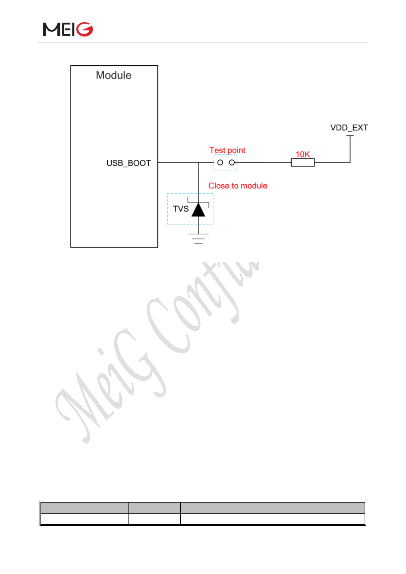
MeiGProductManualofSLM750Module
SLM750ModuleHardwareDesign Page 58, total 84 pages
The following figure shows reference Circuit of USB_ROOT Interface:
Figure 26 Circuit of USB_ROOT Interface
4 GNSS
4.1 General Description
SLM750 includes an integrated embedded GNSS solution that supports Gen8C-Lite of
Qualcomm (GPS, GLONASS, BeiDou).
SLM750 supports standard NMEA-01830183 protocol, and outputs NMEA sentences with
1Hz via USB interface by default.
4.2 GNSS Performance
The following table shows SLM750 GNSS performance.
Table 23: GNSS performance
Parameter Description Performance index
Positioning accuracy Horizon <2m(50%); <5m (90%)
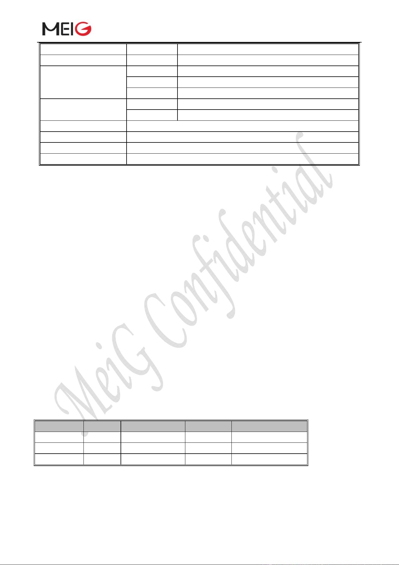
MeiGProductManualofSLM750Module
SLM750ModuleHardwareDesign Page 59, total 84 pages
4.3 Layout Guideline
You need to follow the layout guidelines in the below when designing:
Maximize the distance between the GNSS antenna, the main antenna and the diversity
antenna.
Noisy digital circuits such as the USIM card, USB interface, Camera module, Display
connector and SD card should be kept away from the antenna.
Use ground vias around the GNSS trace and sensitive analog signal traces to provide
isolation and protection.
Keep 50ohm characteristics impedance of the ANT_GNSS trace.
See Chapter 5 for GNSS reference design and antenna consideration.
5 Antenna Interface
Table 24: RF antenna pin definition
Pin name Pin no. Description I/O Note
ANT_MAIN
49
Main antenna
IO
50Ω impedance
ANT_DIV
35
Diversity antenna
AI
50Ω impedance
ANT_GNSS
47
GNSS antenna AI 50Ω impedance
5.1 Antenna Interface
SLM750 provides 3 antenna pins: ANT_MAIN, ANT_DIV, ANT_GNSS. Select connection
(open) Altitude <4m (50%); <8m (90%)
Speed accuracy Speed <0.2m/s
First positioning time
TTFF
Cold start 32s
Warm start 29s
Hot start 2s
Sensitivity Capturing -154dBm
Tracking -156dBm
Serial output baud rate 300bit/s~230400bit/s
GPS receiving 12 channel,GPS L1(1575.42MHz),C/A code
Data update rate 1Hz
Data format NMEA 0183

MeiGProductManualofSLM750Module
SLM750ModuleHardwareDesign Page 60, total 84 pages
diversity antenna to improve WCDMA/TDD-LTE/FDD-LTE receiving performance of the product.
It is recommended that you use a 50Ω impedance antenna that matches the RF connector of the
module.
Special note: In order to ensure the communication ability of all frequency bands,
connect both the main and the auxiliary antennas.
It is suggested that you chose RF adapter carefully on application end. It is necessary to select
the smallest possible loss of the RF adapter, and the recommended RF adapters are as follows:
GSM900/850<1.5dB
DCS1800/PCS1900<1.5dB
CDMA/EVDO<1dB
WCDMA<1.5dB
TD-SCDMA<1.5dB
TD-LTE<1.5dB
FDD LTE<1.5dB
5.2 RF Reference Circuit
ANT_MAIN and ANT_DIV antenna connection reference design circuit are shown as below.
In order to gain better RF performance, you need to reserve n type matching circuit without
mounting capacitor.
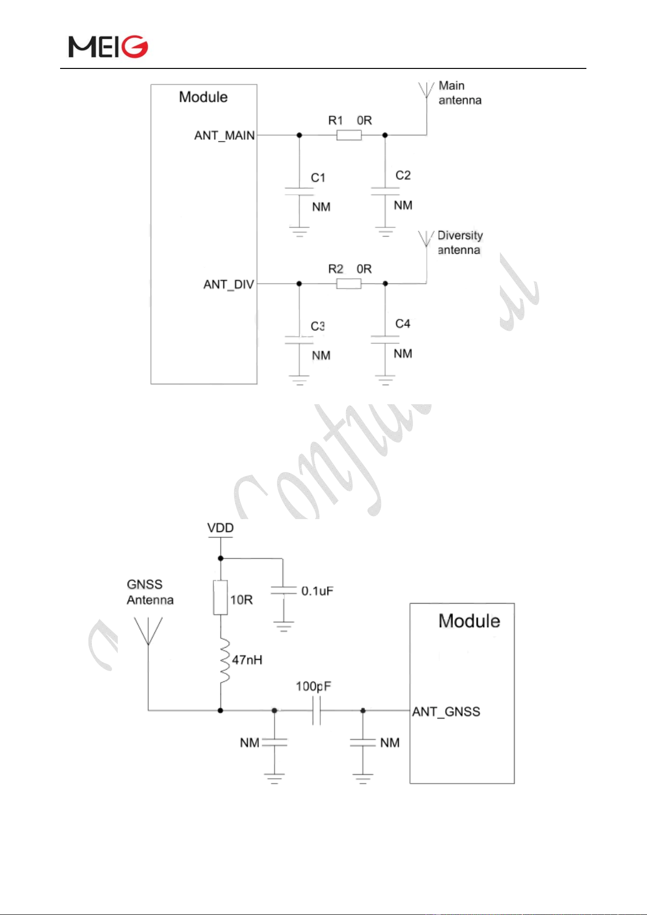
MeiGProductManualofSLM750Module
SLM750ModuleHardwareDesign Page 61, total 84 pages
Figure 27 RF reference circuit
GNSS antenna reference design is shown as below:
Figure 28 GNSS antenna reference circuit
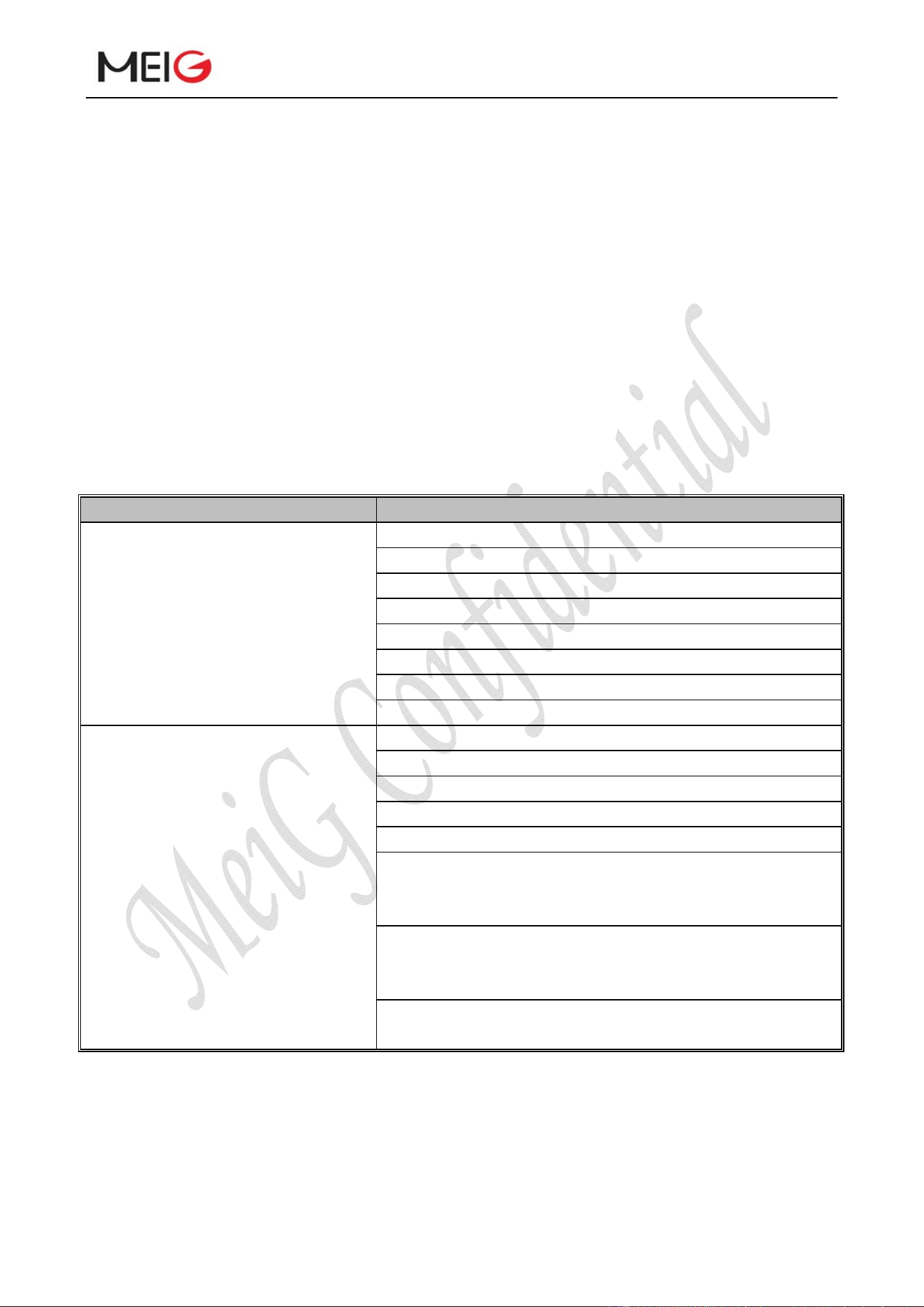
MeiGProductManualofSLM750Module
SLM750ModuleHardwareDesign Page 62, total 84 pages
Note:
1. You can choose external LDO power supply according to active antenna.
2. You can choose passive antenna design so you do not need to design VDD circuit.
5.3 Antenna Installation
5.3.1 Antenna requirements
The main antenna, diversity antenna and GNSS antenna requirements are as follows:
Table 25: Antenna requirements
Type Requirement
GNSS
Frequency range: 1561-1615MHz
Polarization: RHCP or linear
VSWR: < 2(Typ.)
Passive antenna gain: > 0 dBi
Active antenna noise coefficient: < 1.5 dB
Active antenna gain: < -2 dBi
Active antenna embedded LNA gain: 18.5dB(Typical value)
Active antenna total gain: > 18.5 dB(Typical value)
GSM/WCDMA
/TD-SCDMA/CDMA /TD-LTE/FDD
LTE
VSWR: < 2
Gain(dBi): 1
Maximum input power(W): 50
Input impedance(ohm): 50
Polarization type: vertical
Cable insertion loss: < 1.5dB
(GSM850/900,WCDMAB5/B8, CDMA BC0,
LTE B5/ B8/B12/B13/B17/B20/B26)
Cable insertion loss: < 1.5dB
(GSM1800/1900,WCDMA B1/B2/B4, TD-SCDMA B34/B39,
LTE B1/B2/B3/B4/B25/B39, CMDA BC1)
Cable insertion loss: < 2dB
(LTE B7/B38/B40/B41)
5.3.2 RF output power
RF output power of SLM750 is shown as below:
MeiGProductManualofSLM750Module
SLM750ModuleHardwareDesign Page 63, total 84 pages
Table 26: RF output power
Network mode Band Max Min
GSM 900(GMSK) 33dBm ± 2dB 5dBm ± 5dB
1800(GMSK) 30dBm ± 2dB 0dBm ± 5dB
900(8-PSK) 27dBm ± 3dB 5dBm ± 5dB
1800(8-PSK) 26dBm +3/-4dB 0dBm ± 5dB
CDMA BC0 23-30dBm ≤-50 dBm/1.23MHz
EVDO BC0 23-30dBm ≤-50 dBm/1.23MHz
WCDMA Band1 24dBm +1/-3dB -56dBm ± 9dB
Band8 24dBm +1/-3dB -56dBm ± 9dB
TD-SCDMA Band34 24dBm +1/-3dB ≤-40 dBm
Band39 24dBm +1/-3dB ≤-40 dBm
TD-LTE Band38 23dBm ± 2.7 dB ≤-40 dBm
Band39 23dBm ± 2.7 dB ≤-40 dBm
Band40 23dBm ± 2.7 dB ≤-40 dBm
Band41 23dBm ± 2.7 dB ≤-40 dBm
FDD LTE Band1 23dBm ± 2.7 dB ≤-40 dBm
Band3 23dBm ± 2.7 dB ≤-40 dBm
Band5 23dBm ± 2.7 dB ≤-40 dBm
Band8 23dBm ± 2.7 dB ≤-40 dBm
Band28 23dBm ± 2.7 dB ≤-40 dBm
5.3.3 RF receiving sensitivity
Table 27: RF receiving sensitivity
Network mode Band Main Diversity
GSM 900 -109dBm Not Supported
1800 -108dBm Not Supported
WCDMA Band1 -109dBm Not Supported
Band5 -110dBm Not Supported
Band8 -110dBm Not Supported
TD-SCDMA Band34 -109dBm Not Supported
Band39 -109dBm Not Supported
TD-LTE Band38 (10M) -98dBm -98dBm
Band39 (10M) -98dBm -98dBm
Band40 (10M) -98dBm -98dBm
Band41 (10M) -96.5dBm -97dBm
FDD LTE Band1 -98dBm -99dBm
Band3 -98dBm -98dBm
Band5 -99dBm -99dBm
Band8 -99dBm -99dBm
MeiGProductManualofSLM750Module
SLM750ModuleHardwareDesign Page 64, total 84 pages
5.3.4 Operating frequency
Table 28: Operating frequency
Network mode Band Receive Transmit
GSM 850 869~894MHz 824~849MHz
900 925~960MHz 880~915MHz
1800(DCS) 1805~1880MHz 1710~1785MHz
1900(PCS) 1930~1990MHz 1850~1910MHz
WCDMA Band1 2110~2170MHz 1920~1980MHz
Band8 926~960MHz 880~915MHz
TD-SCDMA Band34 2010~2025MHZ 2010~2025MHZ
Band39 1880~1920MHz 1880~1920MHz
TD-LTE Band38 2570~2620MHz 2570~2620MHz
Band39 1880~1920MHz 1880~1920MHz
Band40 2300~2400MHz 2300~2400MHz
Band41 2555~2655MHz 2550~2650MHz
FDD LTE Band1 2110~2170MHz 1920~1980MHz
Band3 1805~1880MHz 1710~1785MHz
Band5 869~894MHz 824~849MHz
Band28 925~960MHz 880~915MHz
CDMA BC0 758~803MHz 703~748MHz
EVDO BC0 869~894MHz 824~849MHz
5.3.5 Antenna requirements
Table 29: Antenna requirements
Network
Mode
Band VSWR Gain Effi. SAR TRP
(dBm)
TIS
(dBm)
Peak Avg.
GSM 850 <2.5: 1 >0dBi >-4dBi >40% <1.6
W/Kg
29 <-102
900 26 <-102
1800(DCS) <-102
1900(PCS) <-102
WCDMA Band1 19 <-102
Band8 19 <-104
CDMA BC0 19 <-104
EVDO BC0 19 <-104
TD-SCDMA Band34 19 <-104
Band39 19 <-104
TD-LTE Band38 19 <-94
MeiGProductManualofSLM750Module
SLM750ModuleHardwareDesign Page 65, total 84 pages
Band39 19 <-94
Band40 19
<-94
Band41 19
<-94
FDD LTE Band1 19
<-92
Band3 19
<-93
Band5 19
<-92
Band8 19
<-92
Band28 19
<-92
Table 30: Diversity antenna requirements
Mode Band VSWR Gain /Avg. Efficiency ρ Isolation
WCDMA Band1 <2.5: 1 >-7dBi >20% <0.5 <-8dB
Band8
TD-LTE Band38
Band39
Band40
Band41
FDD LTE Band1
Band3
Band5
Band8
Band28
6 Electrical characteristics
6.1 Limit voltage range
Limit voltage range refers to the maximum voltage range of the module’s power supply
voltage as well as the digital and analog input/output interfaces. Operate beyond the range may
cause damage to the product.
Limit voltage range of SLM750 are shown as below:
Table 31: Limit voltage range
Parameter Description Min Type Max Unit
VBAT SLM750V power supply 3.3 3.8 4.2 V
Average power supply current of
RMS
0 0.9 A
VBAT_BB maximum current 0 0.8 A
MeiGProductManualofSLM750Module
SLM750ModuleHardwareDesign Page 66, total 84 pages
VBAT_RF maximum current 0 1.8 A
Instantaneous voltage drop
(GSM 900 Maximum transmission
power level)
400 mV
USB_VBUS USB detection 3.0 5.0 5.25 V
GPIO Level power supply voltage of
digital IO
-0.3 1.8 2.0 V
Power supply voltage of shutdown
mode
-0.25 0.25 V
6.2 Temperature range
It is recommended that you use SLM750 at -30℃~+75℃ and take temperature control
measures when applications are in the harsh environment conditions. At the same time, a limited
operating temperature range of the module should be provided. Under this temperature conditions,
some of the indicators may exceed. It is suggested that you store the applications under certain
temperature conditions. Modules beyond this range may not work or are damaged.
Table 32: Temperature range
Parameter Min Type Max Unit
Operation temperature -30 +25 +75 ℃
Limited operation
temperature
-40~-30 75~+85 ℃
Storage temperature -45 +90 ℃
6.3 Electrical Characteristics of Interface Operation Status
VL: logical low level
VH: logical high level
Table 33: Logical level of normal digital IO signal
Signal VL VH Unit
Min Max Min Max
Digital input -0.3 0.3*Vpin_min 0.3*Vpin_max Vpin_max V
Digital output GND 0.2 Vpin_min-0.2 Vpin V
Note: Vpin_min=1.45V, Vpin_max=2.0V (Vpin is high level digital interface, Vpin=1.8V)
MeiGProductManualofSLM750Module
SLM750ModuleHardwareDesign Page 67, total 84 pages
Table 34: Electrical characteristics in power supply status
Parameter I/O Min Type Max Unit
VBAT I 3.3 3.8 4.2 V
USIM_VDD O 1.7/2.75 1.8/2.85 1.9/2.95 V
6.4 Module Power Consumption Range
The following table shows the consumption of SLM750 in various modes. Contact us if you
need more information about the band.
Table 35: Consumption
PARAMETER DESCRIPTION CONDITION VALUE UNIT
IVBAT
Shut Down
mode
Module shutdown leakage 12 uA
Sleep mode AT+CFUN=0 (USB
disconnected)
2.2 mA
GSM 900 DRX=2 (USB
disconnected)
GSM 900 DRX=9 (USB
disconnected)
2.1
2.25
mA
DCS1800 DRX=2 (USB
disconnected)
DCS1800 DRX=9 (USB
disconnected)
2.2
2.3
mA
GSM 850 DRX=2 (USB
disconnected)
GSM 850 DRX=9 (USB
disconnected)
2.3
2.35
mA
WCDMA Band 1
PF=128(USB disconnected)
WCDMA Band 5
PF=128(USB disconnected)
WCDMA Band 8
PF=128(USB disconnected)
2.2
2.01
2.06
mA
WCDMA Band 1 PF=51
(USB disconnected)
WCDMA Band 5
PF=512(USB disconnected)
WCDMA Band 8
PF=512(USB disconnected)
2.3
2.13
2.2
mA
MeiGProductManualofSLM750Module
SLM750ModuleHardwareDesign Page 68, total 84 pages
LTE-TDD Band 38
PF=128(USB disconnected)
LTE-TDD Band 39
PF=128(USB disconnected)
LTE-TDD Band 40
PF=128(USB disconnected)
LTE-TDD Band 41
PF=128(USB disconnected)
2.3
2.1
2.15
2.26
mA
LTE-TDD Band 38
PF=256(USB disconnected)
LTE-TDD Band 39
PF=256(USB disconnected)
LTE-TDD Band 40
PF=256(USB disconnected)
LTE-TDD Band 41
PF=256(USB disconnected)
2.1
2.12
2.2
2.34
mA
LTE-FDD Band 1
PF=128(USB disconnected)
LTE-FDD Band 3
PF=128(USB disconnected)
LTE-FDD Band 5
PF=128(USB disconnected)
LTE-FDD Band 8
PF=128(USB disconnected)
LTE-FDD Band 20
PF=128(USB disconnected)
2.02
2.1
2.16
2.1
2.2
mA
LTE-FDD Band 1
PF=256(USB disconnected)
LTE-FDD Band 3
PF=256(USB disconnected)
LTE-FDD Band 5
PF=256(USB disconnected)
LTE-FDD Band 8
PF=256(USB disconnected)
LTE-FDD Band 20
PF=256(USB disconnected)
1.98
2
2.13
2.25
2.06
mA
Idle mode GSM 900 DRX=5 (USB
disconnected)
GSM 900 DRX=5 (USB
connected)
19.2
32
mA
DCS1800 DRX=5 (USB
disconnected)
DCS1800 DRX=5 (USB
connected)
20
35.2
mA
MeiGProductManualofSLM750Module
SLM750ModuleHardwareDesign Page 69, total 84 pages
GSM 850 DRX=5 (USB
disconnected)
GSM 850 DRX=5 (USB
connected)
19.8
38.6
mA
WCDMA Band 1
PF=64(USB disconnected)
WCDMA Band 1
PF=64(USB connected)
19.2
39.2
mA
WCDMA Band 5 PF=
64(USB disconnected)
WCDMA Band 5 PF=
64(USB connected)
20.2
39.6
mA
WCDMA Band 8 PF=
64(USB disconnected)
WCDMA Band 8 PF=
64(USB connected)
18.6
38.7
mA
TD-SCDMA Band 34
PF=64(USB disconnected)
TD-SCDMA Band 34
PF=64(USB connected)
21
33.6
mA
TD-SCDMA Band 39
PF=64(USB disconnected)
TD-SCDMA Band 39
PF=64(USB connected)
25
36.8
mA
LTE-TDD Band 38
PF=64(USB disconnected)
LTE-TDD Band 38
PF=64(USB connected)
20.9
45.1
mA
LTE-TDD Band 39
PF=64(USB disconnected)
LTE-TDD Band 39
PF=64(USB connected)
21.3
43.6
mA
LTE-TDD Band 40
PF=64(USB disconnected)
LTE-TDD Band 40
PF=64(USB connected)
23
45.8
mA
LTE-TDD Band 41
PF=64(USB disconnected)
LTE-TDD Band 41
PF=64(USB connected)
20.5
43.2
mA
LTE-FDD Band 1
PF=64(USB disconnected)
LTE-FDD Band 1
PF=64(USB connected)
22.8
46.9
mA
MeiGProductManualofSLM750Module
SLM750ModuleHardwareDesign Page 70, total 84 pages
LTE-FDD Band 3
PF=64(USB disconnected)
LTE-FDD Band 3
PF=64(USB connected)
28
48.5
mA
LTE-FDD Band 5
PF=64(USB disconnected)
LTE-FDD Band 5
PF=64(USB connected)
27.6
49.2
mA
LTE-FDD Band 8
PF=64(USB disconnected)
LTE-FDD Band 8
PF=64(USB connected)
24.9
48.6
mA
LTE-FDD Band 20
PF=64(USB disconnected)
LTE-FDD Band 20
PF=64(USB connected)
22.7
49.8
mA
GPRS data
transfer
(GNSS
shut down)
GSM850
156.2 mA
GSM850
230 mA
GSM850
305.3 mA
GSM850
388.2 mA
EDGE data
transfer (GNSS
shut down)
GSM900
175.9 mA
GSM900
277.7 mA
GSM900
367.7 mA
GSM900
479.8 mA
DCS1800
151.8 mA
DCS1800 222.1 mA
MeiGProductManualofSLM750Module
SLM750ModuleHardwareDesign Page 71, total 84 pages
DCS1800
295.5 mA
DCS 1800
363.2 mA
GSM 850
186.3 mA
GSM 850
282.3 mA
GSM 850
381.1 mA
GSM 850
482.7 mA
WCDMA data
transfer
WCDMA Band 1
434.7 mA
WCDMA Band 1
426 mA
WCDMA Band 5
529.6 mA
WCDMA Band 5
512.9 mA
WCDMA Band 8
508.2 mA
WCDMA Band 8
495 mA
LTE data
transfer
FDD- LTE Band 1
497.2 mA
FDD- LTE Band 3
600.3 mA
FDD- LTE Band 5
585.8 mA
FDD- LTE Band 8
590.6 mA
FDD- LTE Band 20
600.3 mA
TDD- LTE Band 38
412.5 mA
TDD- LTE Band 39
394.8 mA
TDD- LTE Band 40
376.8 mA
TDD- LTE Band 41
392 mA
MeiGProductManualofSLM750Module
SLM750ModuleHardwareDesign Page 72, total 84 pages
GSM voice call GSM900 PCL=5 @32.21dBm 237.1 mA
DCS1800 PCL=0 @28.14dBm 200.7 mA
GSM850 PCL=5 @32.12dBm 243.9 mA
CDMA voice
call
BC0 @20.31dBm 556 mA
WCDMA voice
call
6.5 Environmental Reliability Requirements
Table 36: Environmental reliability requirements
Test item Test condition
Low temperature
storage test
-45℃, last for 24 hours in shutdown mode
High temperature
storage test
+90℃, last for 24 hours in shutdown mode
Temperature impact
test
In shutdown mode, last for 1 hour in -45℃ and +90℃. Temperature
conversion time is <3min, total 24 cycles.
High temperature high
humidity test
+85℃,95%RH,last for 48 hours in shutdown mode
Low temperature
operation test
-30℃,last for 24 hours in operation mode
High temperature
operation test
+75℃,last for 24 hours in operation mode
Vibration test Perform vibration tests as required in the following table:
Frequency Random vibration ASD(Acceleration
spectral density)
5~20Hz 0.96m
2
/s
3
20~500Hz 0.96m
2
/s
3
(20Hz),other -3dB/times
frequency range
Connector life test Board to board connector interface plugging 50 times; RF antenna
interface cable plugging 30 times
ESD test 1、The module tests the power PAD and the large area in the call
state, ESD meets:
1) Contact discharge shall pass ±4KV、±5KV test grade
2) Air discharge shall pass ±8KV、±10KV test grade
2、the module tests SIM card connector of EVB in shutdown mode,
ESD meets:
MeiGProductManualofSLM750Module
SLM750ModuleHardwareDesign Page 73, total 84 pages
1) Contact discharge shall pass ±4KV test grade
2) Air discharge shall pass ±8KV test grade
3、the module tests other interfaces, ESD meets:
1) Air discharge shall pass ±0.5KV test grade
2) Air discharge shall pass ±1KV test grade
6.6 ESD Characteristics
SLM750 is a consumer terminal product. Although we have considered possible problems of
ESD and took some protections, considering problems in the transport and secondary development,
we need to consider the protection of final product ESD, including the anti electrostatic packaging
processing. You can refer to the recommended circuit of interface design in the document when
using in applications.
The following table shows the discharge range of SLM750 ESD:
Table 37: ESD performance parameters (Temperature: 25℃, Humidity: 45%)
Tes t point Contact discharge Air discharge Unit
VBAT, GND ±5 ±10 KV
Antenna interfaces ±4 ±8 KV
Other interfaces ±0.5 ±1 KV
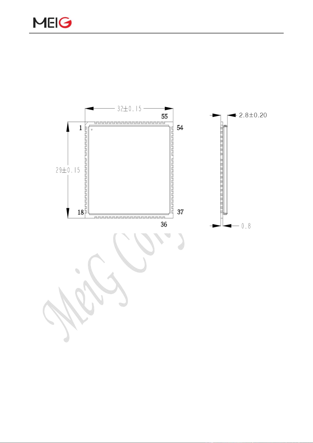
MeiGProductManualofSLM750Module
SLM750ModuleHardwareDesign Page 74, total 84 pages
7 Mechanical Dimensions
7.1 Mechanical Dimensions of the Module
Figure 29 Module top and side dimension (unit: mm)
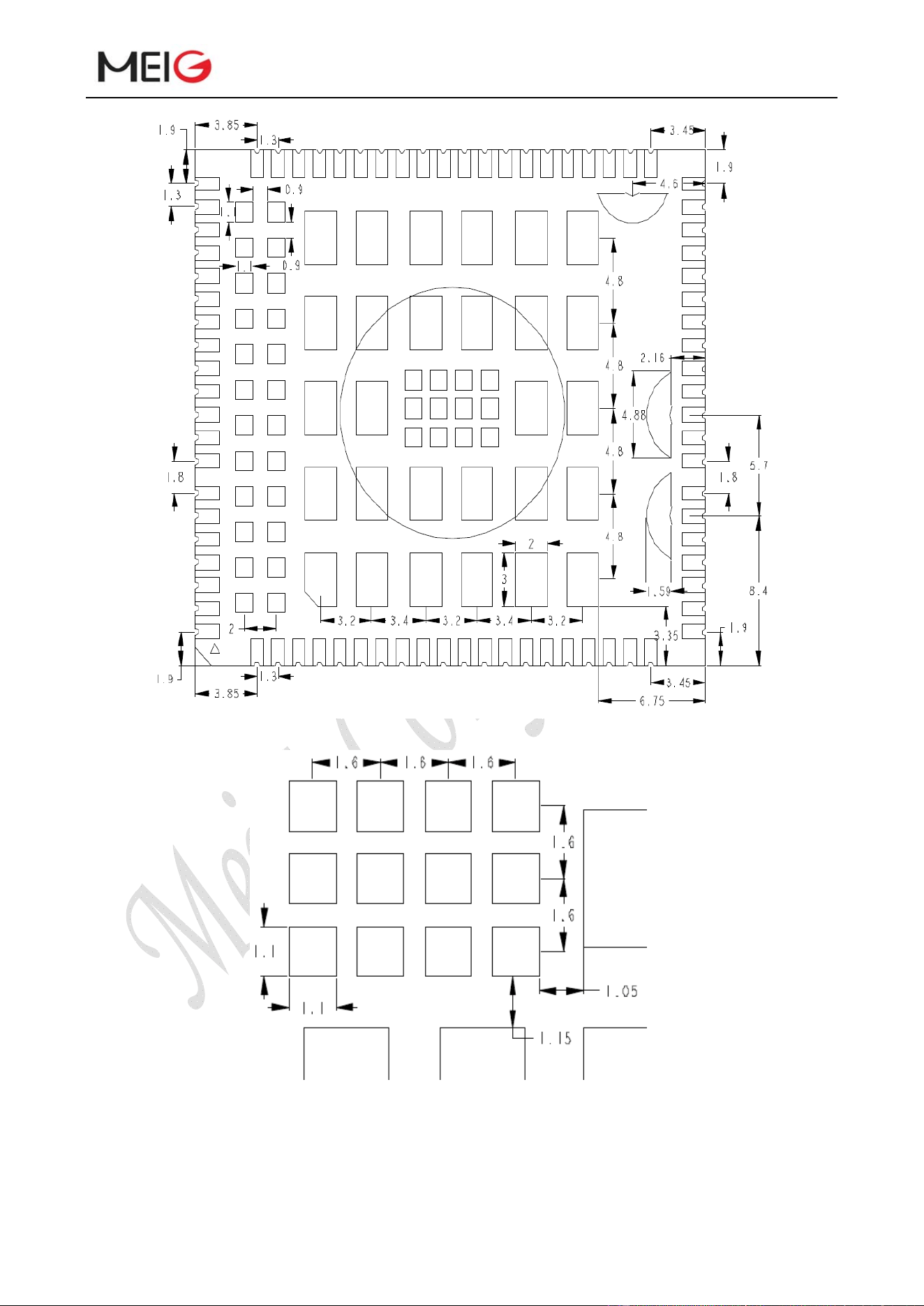
MeiGProductManualofSLM750Module
SLM750ModuleHardwareDesign Page 75, total 84 pages
Figure 30 Module bottom dimensions (unit: mm)
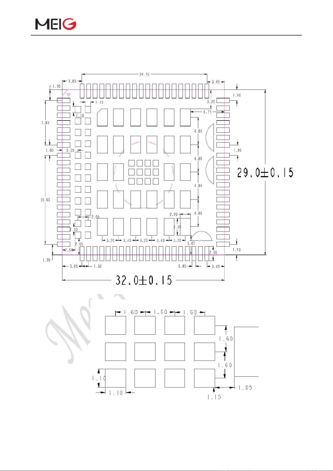
MeiGProductManualofSLM750Module
SLM750ModuleHardwareDesign Page 76, total 84 pages
7.2 Recommended Packaging
Figure 31 Top view of recommended packaging (unit: mm)
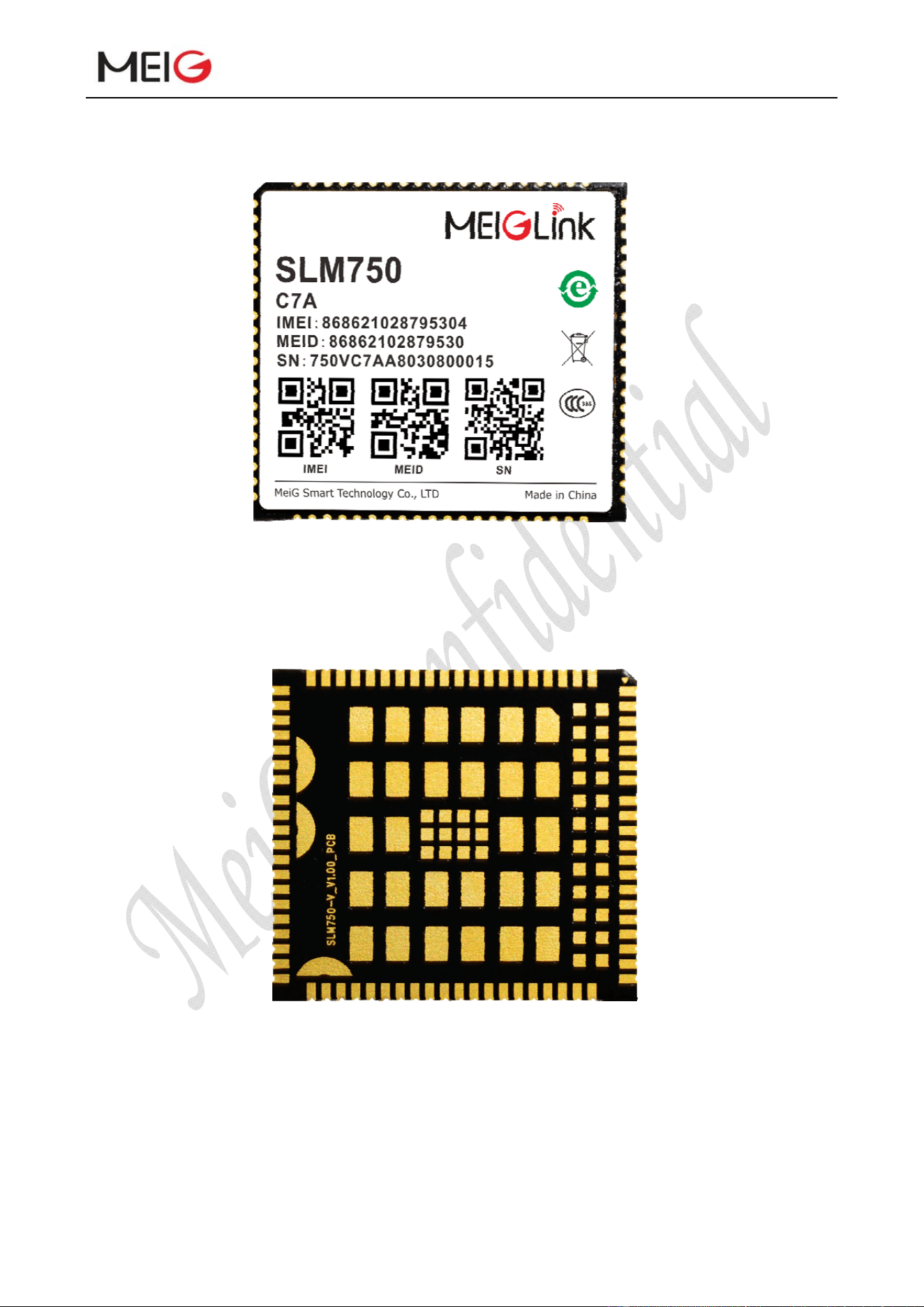
MeiGProductManualofSLM750Module
SLM750ModuleHardwareDesign Page 77, total 84 pages
7.3 Top View of the Module
Figure 32 Top view of the module
7.4 Bottom View of the Module
Figure 33 Bottom view of the module

MeiGProductManualofSLM750Module
SLM750ModuleHardwareDesign Page 78, total 84 pages
8 Storage and Manufacturing
8.1 Storage
SLM750 is stored in sealed vacuum bag. The restrictions of storage condition are shown as
below:
1. Shelf life in sealed bag is 12 months at <40℃/90%RH.
2. After this bag is open, devices that will be subjected to reflow soldering or other high
temperature processes must be:
Stored at <10%RH.
Mounted within 72 hours at factory conditions of ≤ 30℃/60%RH.
3. Devices require baking before mounting, if:
Humidity indicator card is >10% when ambient temperature is 23℃±5℃.
Mounting cannot be finished within 72 hours at factory conditions of ≤ 30℃/60% RH.
Stored at >10%RH.
4. If baking is required, devices may be baked for 48 hours at 125℃±5℃.
Note: As plastic packaging cannot stand the high temperatures, the package must be removed
from devices before baking.
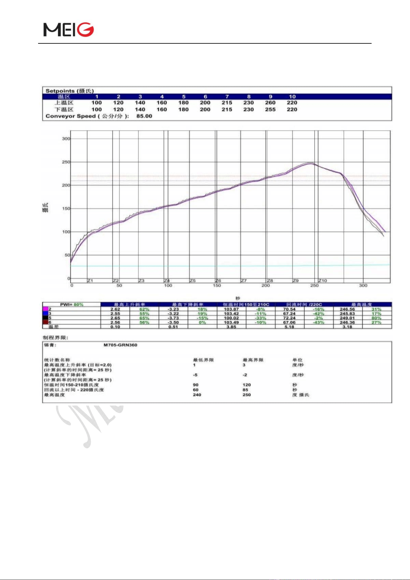
MeiGProductManualofSLM750Module
SLM750ModuleHardwareDesign Page 79, total 84 pages
8.2 Manufacturing and Welding
Figure 34 Reflow soldering temperature profile
8.3 Packing
SLM750 uses pallet packaging. Specifications are as follows:
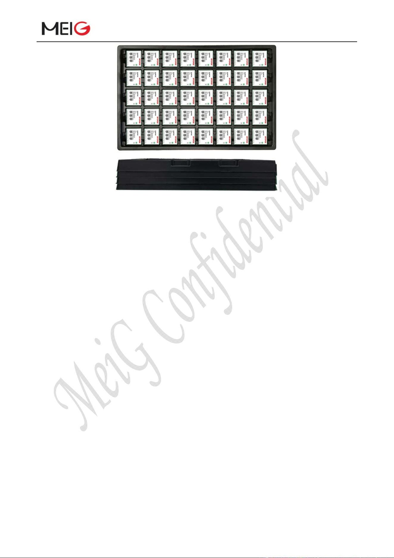
MeiGProductManualofSLM750Module
SLM750ModuleHardwareDesign Page 80, total 84 pages
Figure 35 Pallet packaging(Unit: mm)
MeiGProductManualofSLM750Module
SLM750ModuleHardwareDesign Page 81, total 84 pages
9 Appendix A References
9.1 Related Documents
SLM750 specifications;
SLM750 AT command set;
SLM750 EVB user manual;
SLM750 reference design circuit;
SLM750 application service process manual.
9.2 Terms and Abbreviations
Table 38: Terms and abbreviations
Abbreviations Descriptions
AMR Adaptive Multi-rate
BER Bit Error Rate
BTS Base Transceiver Station
PCI Peripheral Component Interconnect
CS Circuit Switched (CS) domain
CSD Circuit Switched Data
DCE Data communication equipment
DTE Data terminal equipment
DTR Data Terminal Ready
EDGE Enhanced Data rates for GSM Evolution
EFR Enhanced Full Rate
EGSM Enhanced GSM
EMC Electromagnetic Compatibility
ESD Electrostatic Discharge
FR Frame Relay
GMSK Gaussian Minimum Shift Keying
GPIO General Purpose Input Output
GPRS General Packet Radio Service
GSM Global Standard for Mobile Communications
HR Half Rate
HSDPA High Speed Downlink Packet Access
HSUPA High Speed Uplink Packet Access
HSPA HSPA High-Speed Packet Access
HSPA+ HSPA High-Speed Packet Access+
MeiGProductManualofSLM750Module
SLM750ModuleHardwareDesign Page 82, total 84 pages
IEC International Electro-technical Commission
IMEI International Mobile Equipment Identity
MEID Mobile Equipment Identifier
I/O Input/Output
ISO International Standards Organization
ITU International Telecommunications Union
bps bits per second
LED Light Emitting Diode
M2M Machine to machine
MO Mobile Originated
MT Mobile Terminated
NTC Negative Temperature Coefficient
PC Personal Computer
PCB Printed Circuit Board
PCS Personal Cellular System
PCM Pulse Code Modulation
PCS Personal Communication System
PDU Packet Data Unit
PPP Point-to-point protocol
PS Packet Switched
QPSK Quadrate Phase Shift Keying
SIM Subscriber Identity Module
TCP/IP Transmission Control Protocol/ Internet Protocol
UART Universal asynchronous receiver-transmitter
USIM Universal Subscriber Identity Module
UMTS Universal Mobile Telecommunications System
USB Universal Serial Bus
WCDMA Wideband Code Division Multiple Access
TD-SCDMA Time Division-Synchronous Code Division Multiple Access
TD-LTE Time Division Long Term Evolution
FDD LTE Frequency Division Duplexing Long Term Evolution
Vmax Maximum Voltage Value
Vnorm Normal Voltage Value
Vmin Minimum Voltage Value
V
IH
max Maximum Input High Level Voltage Value
V
IH
min Minimum Input High Level Voltage Value
V
IL
max Maximum Input Low Level Voltage Value
V
IL
min Minimum Input Low Level Voltage Value
V
OH
max Maximum Output High Level Voltage Value
V
OH
min Minimum Output High Level Voltage Value
V
OL
max Maximum Output Low Level Voltage Value
V
OL
min Minimum Output Low Level Voltage Value
MeiGProductManualofSLM750Module
SLM750ModuleHardwareDesign Page 83, total 84 pages
10 Appendix B GPRS Coding Scheme
Table 39: Description of coding schemes
Mode CS-1 CS-2 CS-3 CS-4
Coding speed 1/2 2/3 3/4 1
USF 3 3 3 3
Pre-coded USF 3 6 6 12
Radio Block excl.USF and BCS 181 268 312 428
BCS 40 16 16 16
Tail 4 4 4 -
Coded Bits 456 588 676 456
Punctured Bits 0 132 220 -
Data rate Kb/s 9.05 13.4 15.6 21.4
FCC Statement
FCC Label: The FCC ID is on the front of the device. It is easily visible.
The device FCC ID is 2APJ4-SLM750V.
A label with the following statements must be attached to the host end product:
This device contains FCC ID: 2APJ4-SLM750V.
The manual provides guidance to the host manufacturer will be included in the documentation that
will be provided to the OEM.
The module is limited to installation in mobile or fixed applications.
The separate approval is required for all other operating configurations, including portable
configurations and different antenna configurations.
The OEM integrators are responsible for ensuring that the end-user has no manual or instructions to
remove or install module.
Module grantee (the party responsible for the module grant) shall provide guidance to the host
manufacturer for ensuring compliance with the Part 15 Subpart B requirements.
The host manufacturer is responsible for additional testing to verify compliance as a composite
system. When testing the host device for compliance with the Part 15 Subpart B requirements, the
host manufacturer is required to show compliance with the Part 15 Subpart B while the transmitter
module(s) are installed and operating. The modules should be transmitting and the evaluation
should confirm that the module’s intentional emissions are compliant (i.e. fundamental and out of

MeiGProductManualofSLM750Module
SLM750ModuleHardwareDesign Page 84, total 84 pages
band emissions) with the Radio essential requirements. The host manufacturer must verify that there
are no additional unintentional emissions other than what is permitted in the Part 15 Subpart B or
emissions are complaint with the Radio aspects.
FCC RF Exposure Requirements
This device complies with FCC RF radiation exposure limits set forth for an uncontrolled
environment.
The antenna(s) used for this transmitter must not be co-located or operating in conjunction with any
other antenna or transmitter and must be installed to provide a separation distance of at least 20cm
from all persons.
FCC Regulations
This device complies with part 15 of the FCC Rules. Operation is subject to the following two
conditions: (1) This device may not cause harmful interference, and (2) this device must accept any
interference received, including interference that may cause undesired operation.
This device has been tested and found to comply with the limits for a Class B digital device,
pursuant to Part 15 of the FCC Rules.
These limits are designed to provide reasonable protection against harmful interference in a
residential installation. This equipment generates, uses and can radiate radio frequency energy and,
if not installed and used in accordance with the instructions, may cause harmful interference to
radio communications.
EU DECLARATION OF CONFORMITY
Hereby, MeiG Smart Technology Co., Ltd declares that the radio
equipment type SLM750 is in compliance with Directive 2014/53/EU.
The most recent and valid version of the DoC (Declaration of Conformity) can be
viewed at www.meigsmart.com/en/product-certification.

Requirement per KDB 996369 D03
The device complies with KDB 996369 D03 OEM Manual v01. Below are integration instructions
for host product manufacturers according to the KDB 996369 D03 OEM Manual v01.
List of Applicable FCC Rules
FCC CFR 47 Part 22H/ FCC CFR 47 Part 24E/ FCC CFR 47 Part 27C/ FCC CFR 47 Part 90R
Specific Operational Use Conditions
The module has GSM/WCDMA and LTE functions.
• Operation Frequency:
Bands Tx (MHz) Rx (MHz)
GSM850 824 ~ 849 869 ~ 894
GSM1900 1850 ~ 1910 1930 ~ 1990
WCDMA Band II 1850 ~ 1910 1930 ~ 1990
WCDMA Band IV 1710 ~ 1755 2110 ~ 2155
WCDMA Band V 824 ~ 849 869 ~ 894
LTE Band 2 1850 ~ 1910 1930 ~ 1990
LTE Band 4 1710 ~ 1755 2110 ~ 2155
LTE Band 5 824 ~ 849 869 ~ 894
LTE Band 12 699 ~ 716 729 ~ 746
LTE Band 13 777 ~ 787 746 ~ 756
LTE Band 14 788 ~ 798 758 ~ 768
LTE Band 25 1850 ~ 1915 1930 ~ 1995
LTE Band 41 2496 ~ 2690 2496 ~ 2690
LTE Band 66 1710 ~ 1780 2110 ~ 2180
LTE Band 71 663 ~ 698 617 ~ 652
• Modulation:
GSM/GPRS: GMSK, EGPRS: GMSK/ 8PSK; WCDMA: QPSK,16QAM; LTE: QPSK, 16QAM
• Type: External Antenna
• Gain:
GSM850: -0.8dBi; GSM1900: 0.8dBi
WCDMA Band II: -0.8dBi; WCDMA Band IV: -1.4dBi; WCDMA Band V: -0.8dBi
LTE Band 2: -0.8dBi; LTE Band 4: -1.4dBi; LTE Band 5: -0.8dBi; LTE Band 12: 1.3dBi
LTE Band 13: 1.7dBi; LTE Band 14: 1.7dBi; LTE Band 25: -0.8dBi; LTE Band 41: 2.4dBi
LTE Band 66: -1.4dBi; LTE Band 71: 0.3dBi
The module can be used for applications with maximum antenna gain. The host manufacturer
installing this module into their product must ensure that the final composite product complies
with the FCC requirements by a technical assessment or evaluation of the FCC rules, including the
transmitter operation. The host manufacturer must be aware not to provide information to the
end user regarding how to install or remove this RF module in the user’s manual of the end product
which integrates this module. The end user manual shall include all required regulatory
information/warning as shown in this manual.
Limited Module Procedures
Not applicable. The module is a single module and complies with the requirement of FCC Part
15.212.
Trace Antenna Designs
Not applicable. The module has its own antenna, and does not need a host’s printed board
microstrip trace antenna, etc.
RF Exposure Considerations
The module must be installed in the host equipment such that at least 20cm is maintained between
the antenna and users’ body; and if RF exposure statement or module layout is changed, then the
host product manufacturer required to take responsibility of the module through a change in FCC
ID or new application. The FCC ID of the module cannot be used on the final product. In these
circumstances, the host manufacturer will be responsible for re-evaluating the end product
(including the transmitter) and obtaining a separate FCC authorization.
Antennas
Antenna specifications are as follows:
• Type: External Antenna
• Gain:
GSM850: -0.8dBi; GSM1900: 0.8dBi
WCDMA Band II: -0.8dBi; WCDMA Band IV: -1.4dBi; WCDMA Band V: -0.8dBi
LTE Band 2: -0.8dBi; LTE Band 4: -1.4dBi; LTE Band 5: -0.8dBi; LTE Band 12: 1.3dBi
LTE Band 13: 1.7dBi; LTE Band 14: 1.7dBi; LTE Band 25: -0.8dBi; LTE Band 41: 2.4dBi
LTE Band 66: -1.4dBi; LTE Band 71: 0.3dBi
This device is intended only for host manufacturers under the following conditions:
• The transmitter module may not be co-located with any other transmitter or antenna.
• The module shall be only used with the external antenna(s) that has been originally tested and
certified with this module.
• The antenna must be either permanently attached or employ a ‘unique’ antenna coupler.
As long as the conditions above are met, further transmitter test will not be required. However,
the host manufacturer is still responsible for testing their end-product for any additional
compliance requirements required with this module installed (for example, digital device emissions,
PC peripheral requirements, etc.).
Label and Compliance Information
Host product manufacturers need to provide a physical or e-label stating “Contains FCC ID:
2APJ4-SLM750VAT” with their finished product.
Information on test modes and additional testing requirements
• Operation Frequency:
Bands Tx (MHz) Rx (MHz)
GSM850 824 ~ 849 869 ~ 894
GSM1900 1850 ~ 1910 1930 ~ 1990
WCDMA Band II 1850 ~ 1910 1930 ~ 1990
WCDMA Band IV 1710 ~ 1755 2110 ~ 2155
WCDMA Band V 824 ~ 849 869 ~ 894
LTE Band 2 1850 ~ 1910 1930 ~ 1990
LTE Band 4 1710 ~ 1755 2110 ~ 2155
LTE Band 5 824 ~ 849 869 ~ 894
LTE Band 12 699 ~ 716 729 ~ 746
LTE Band 13 777 ~ 787 746 ~ 756

LTE Band 14 788 ~ 798 758 ~ 768
LTE Band 25 1850 ~ 1915 1930 ~ 1995
LTE Band 41 2496 ~ 2690 2496 ~ 2690
LTE Band 66 1710 ~ 1780 2110 ~ 2180
LTE Band 71 663 ~ 698 617 ~ 652
• Modulation:
GSM/GPRS: GMSK, EGPRS: GMSK/ 8PSK; WCDMA: QPSK,16QAM; LTE: QPSK, 16QAM
• Type: External Antenna
• Gain:
GSM850: -0.8dBi; GSM1900: 0.8dBi
WCDMA Band II: -0.8dBi; WCDMA Band IV: -1.4dBi; WCDMA Band V: -0.8dBi
LTE Band 2: -0.8dBi; LTE Band 4: -1.4dBi; LTE Band 5: -0.8dBi; LTE Band 12: 1.3dBi
LTE Band 13: 1.7dBi; LTE Band 14: 1.7dBi; LTE Band 25: -0.8dBi; LTE Band 41: 2.4dBi
LTE Band 66: -1.4dBi; LTE Band 71: 0.3dBi
Host manufacturers must perform tests of radiated and conducted emission and spurious emission,
etc., according to the actual test modes for a stand-alone modular transmitter in a host, as well as
for multiple simultaneously transmitting modules or other transmitters in a host product. Only
when all the test results of test modes comply with FCC requirements, then the end product can
be sold legally.