– 1 –
CD-BK3200V
No. S9155CDK3200V
• In the interests of user-safety the set should be restored to its
original condition and only parts identical to those specified be
used.
SERVICE MANUAL
This document has been published to be used
for after sales service only.
The contents are subject to change without notice.
SHARP CORPORATION
NTSC/PAL
CONTENTS
Page
SAFETY PRECAUTION FOR SERVICE MANUAL ........................................................................................................... 2
VOLTAGE SELECTION ..................................................................................................................................................... 2
AC POWER SUPPLY CORD AND AC PLUG ADAPTOR ................................................................................................. 3
SPECIFICATIONS ............................................................................................................................................................. 3
NAMES OF PARTS ........................................................................................................................................................... 4
OPERATION MANUAL ...................................................................................................................................................... 6
DISASSEMBLY .................................................................................................................................................................. 9
REMOVING AND REINSTALLING THE MAIN PARTS ................................................................................................... 12
ADJUSTMENT ................................................................................................................................................................. 13
CD CHANGER MECHANISM MAIN BASE PARTS ASSEMBLING/ADJUSTING PROCEDURE................................... 16
BLOCK DIAGRAM ........................................................................................................................................................... 25
SCHEMATIC DIAGRAM / WIRING SIDE OF P.W.BOARD ............................................................................................. 28
VOLTAGE ........................................................................................................................................................................ 50
NOTES ON SCHEMATIC DIAGRAM .............................................................................................................................. 51
TYPES OF TRANSISTOR AND LED............................................................................................................................... 51
WAVEFORMS OF CD CIRCUIT ...................................................................................................................................... 52
TROUBLESHOOTING ..................................................................................................................................................... 53
FUNCTION TABLE OF IC................................................................................................................................................ 57
FL DISPLAY ..................................................................................................................................................................... 68
REPLACEMENT PARTS LIST/EXPLODED VIEW
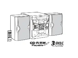
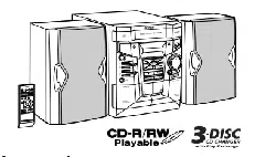
VIDEO CD MINI SYSTEM
MODEL CD-BK3200V
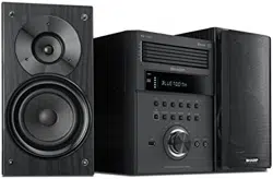
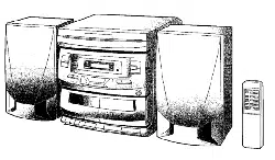
CD-BK3200V Video CD Mini System consisting of
CD-BK3200V (main unit) and CP-BK3200 (speaker system).

CD-BK3200V
– 2 –
SAFETY PRECAUTION FOR SERVICE MANUAL
WARNINGS
THE AEL (ACCESSIBLE EMISSION LEVEL) OF THE LASER POWER OUTPUT IS LESS THAN CLASS 1 BUT THE LASER
COMPONENT IS CAPABLE OF EMITTING RADIATION EXCEEDING THE LIMIT FOR CLASS 1. THEREFORE IT IS
IMPORTANT THAT THE FOLLOWING PRECAUTIONS ARE OBSERVED DURING SERVICING TO PROTECT YOUR EYES
AGAINST EXPOSURE TO THE LASER BEAM.
1-WHEN THE CABINET IS REMOVED, THE POWER IS TURNED ON WITHOUT A COMPACT DISC IN POSITION AND THE
PICKUP IS ON THE OUTER EDGE THE LASER WILL LIGHT FOR SEVERAL SECONDS TO DETECT A DISC. DO NOT
LOOK INTO THE PICKUP LENS.
2-THE LASER POWER OUTPUT OF THE PICKUP UNIT AND REPLACEMENT SERVICE PARTS ARE ALL FACTORY
PRESET BEFORE SHIPMENT.
DO NOT ATTEMPT TO READJUST THE LASER PICKUP UNIT DURING REPLACEMENT OR SERVICING.
3-UNDER NO CIRCUMSTANCES STARE INTO THE PICKUP LENS AT ANY TIME.
4-CAUTION-USE OF CONTROLS OR ADJUSTMENTS, OR PERFORMANCE OF PROCEDURES OTHER THAN THOSE
SPECIFIED HEREIN MAY RESULT IN HAZARDOUS RADIATION EXPOSURE.
VOLTAGE SELECTION
Before operating the unit on mains, check the preset voltage. If the voltage is different from your local voltage, adjust the voltage
as follows.
Turn the selector with a screwdriver until the appropriate voltage number appears in the window (110 V, 127 V, 220 V or 230 V-240 V AC).
Laser Diode Properties
Material: GaAIAs
Wavelength: 780 nm
Emission Duration: continuous
Laser Output: max. 0.6 mW
.
CAUTION-INVISIBLE LASER RADIATION WHEN OPEN. DO NOT STARE INTO BEAM
OR VIEW DIRECTLY WITH OPTICAL INSTRUMENTS.
VARNING-OSYNLIG LASERSTRALNING NAR DENNA DEL AR OPPNAD. STIRRA EJ
IN I STRALEN OCH BETRAKTA EJ STRALEN MED OPTISKA INSTRUMENT.
ADVERSEL-USYNLIG LASERSTRALING VED ABNING. SE IKKE IND I
STRALEN-HELLER IKKE MED OPTISKE INSTRUMENTER.
VARO! AVATTAESSA OLET ALTTIINA NAKYMATON LASERSATEILYLLE. ALA
TUIJOTA SATEESEEN ALAKA KATSO SITA OPTISEN LAITTEEN LAPI.
VARNING-OSYNLIG LASERSTRALNING NAR DENNA DEL AR OPPNAD. STIRRA EJ
IN I STRALEN OCH BETRAKTA EJ STRALEN GENOM OPTISKT INSTRUMENT.
ADVERSEL-USYNLIG LASERSTRALING NAR DEKSEL APNES. STIRR IKKE INN I
STRALEN ELLER SE DIREKTE MED OPTISKE INSTRUMENTER.
– 3 –
CD-BK3200V
General
Amplifier
Video CD
CD player
Tuner
Cassette deck
Power source
AC 110/127/220/230 - 240 V, 50/60 Hz
Power consumption
175 W
Dimensions
Width: 260 mm (10-1/4")
Height: 338 mm (13-5/16")
Depth: 375 mm (14-13/16")
Weight
9.1 kg (20.1 lbs.)
Output power
MPO: 334 W (167 W + 167 W) (10 % T.H.D.)
Main speaker (woofer and tweeter): 134 W (67 W + 67 W)
Subwoofer: 200 W (100 W + 100 W)
RMS: 200 W (100 W + 100 W) (10 % T.H.D.)
Main speaker (woofer and tweeter): 80 W (40 W + 40 W)
Subwoofer: 120 W (60 W + 60 W)
RMS: 184 W (92 W + 92 W) (0.9 % T.H.D.)
Main speaker (woofer and tweeter): 74 W (37 W + 37 W)
Subwoofer: 110 W (55 W + 55 W)
Output terminals
Speakers: 6 ohms
Headphones: 16 - 50 ohms (recommended: 32 ohms)
Video out: 1 Vp-p (75 ohms)
Input terminals
Video/Auxiliary (audio signal): 500 mV/47 kohms
Microphone: 1 mV/600 ohms
Video output format
PAL/NTSC
Type
6-disc multi-play compact disc player
Signal readout
Non-contact, 3-beam semiconductor laser pickup
D/A converter
1-bit D/A converter
Frequency response
20- 20,000 Hz
Dynamic range
90 dB (1 kHz)
Frequency range
FM: 88 - 108 MHz
AM: 531 - 1,602 kHz
Frequency response
50 - 14,000 Hz (Normal tape)
Signal/noise ratio
55 dB (TAPE 1, playback)
50 dB (TAPE 2, recording/playback)
Wow and flutter
0.3 % (WRMS)
Type
3-way type speaker system
5 cm (2") Tweeter
13 cm (5-1/4") Woofer
13 cm (5-1/4") Subwoofer
Maximum input power
(Total)
200 W
Rated input power
(Total)
100 W
Impedance
6 ohms
Dimensions
Width: 280 mm (11")
Height: 330 mm (13")
Depth: 272 mm (10-11/16")
Weight
4.8 kg (10.6 lbs.)/each
Specifications for this model are subject to change without
prior notice.
SPECIFICATIONS
CD-BK3200V
CP-BK3200
FOR A COMPLETE DESCRIPTION OF THE OPERATION OF THIS UNIT, PLEASE REFER
TO THE OPERATION MANUAL.
AC POWER SUPPLY CORD AND AC PLUG ADAPTOR
QACCA0003AW00
QACCB0011AW00
QACCE0008AW00
QACCJ0007AW00
QPLGA0003AWZZ
QPLGA0004AWZZ
CD-BK3200V
– 4 –
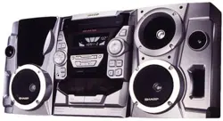
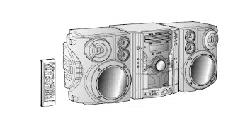
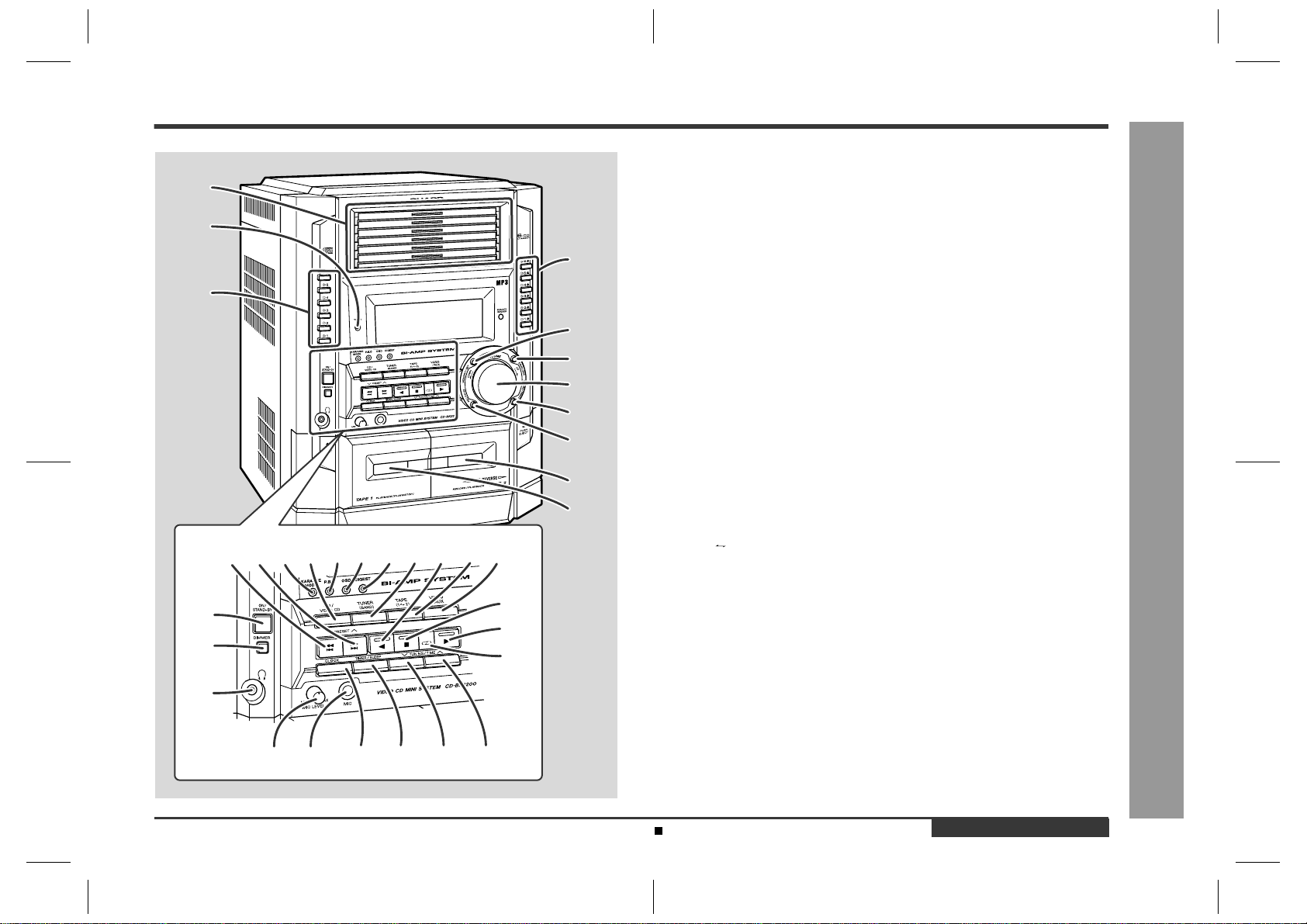
NAMES OF PARTS
CD-BK3200V
Front panel
1. Disc Trays
2. Timer Set Indicator
3. Disc Direct Play Buttons
4. Disc Eject Buttons
5. Memory/Set Button
6. Equalizer Mode Select Button
7. Volume Control
8. Extra Bass/Demo Mode Button
9. Tape 2 Record Pause Button
10. Tape 2 Cassette Compartment
11. Tape 1 Cassette Compartment
12. Video CD Skip or Previous, CD/MP3 Disc Track Down or Fast
Reverse, Tape 2 Fast Wind, Tuner Preset Down Button
13. Video CD Skip or Next, CD/MP3 Disc Track Up or Fast Forward,
Tape 2 Fast Wind, Tuner Preset Up Button
14. Karaoke Mode Button
15. Video CD/CD/MP3 Disc Button
16. Video CD Playback Control Button
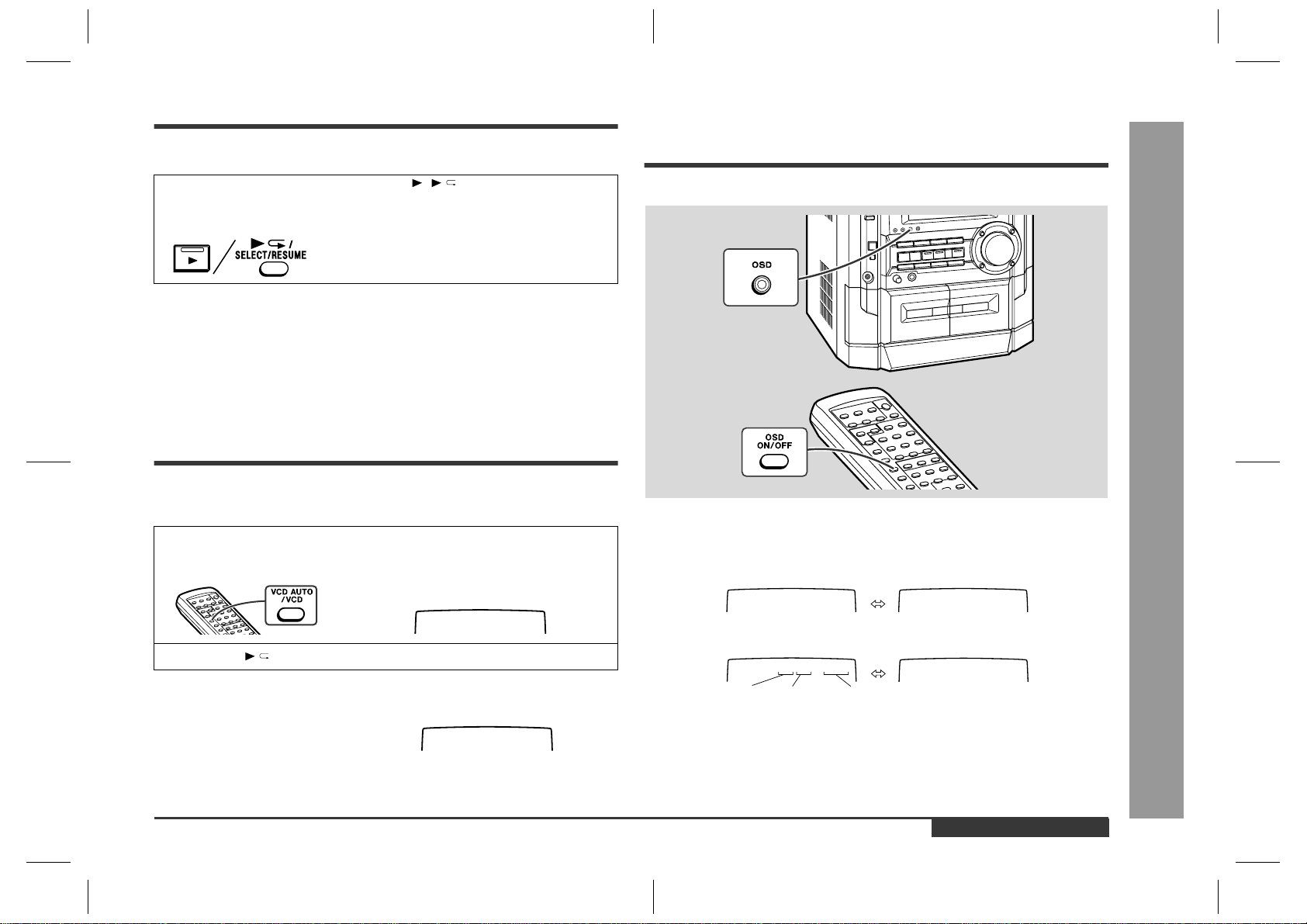
17. Video CD On Screen Display On/Off Button
18. Video CD Digest/Time Search Button
19. Tuner (Band) Button
20. Tape 2 Reverse Play Button (with Indicator)
21. Tape (1 2) Button
22. Video/Auxiliary Button
23. On/Stand-by Button
24. Dimmer Button
25. Headphone Socket
26. Video CD Stop or Return,
CD/MP3 Disc/Tape Stop Button (with Indicator)
27. Video CD Play or Repeat or Select or Resume,
CD/MP3 Disc Play or Repeat, Tape 1 Play,
Tape 2 Forward Play Button (with Indicator)
28. Tape 2 Reverse Mode Select Button
29. Microphone Level Control
30. Microphone Socket
31. Clock Button
32. Timer/Sleep Button
33. Tuning and Time Down Button
34. Tuning and Time Up Button
26
27
28
12
3433323129 30
13 14 151617 1819 20 21
22
23
24
25
1
2
3
4
5
6
7
8
9
10
11
Display
1. Disc Music Schedule Indicators
2. Disc Indicators
3. FM Stereo Mode Indicator
4. FM Stereo Receiving Indicator
5. Memory Indicator
6. Disc Random Play Indicator
7. Tape 2 Record Indicator
8. Extra Bass Indicator
9. Timer Recording Indicator
10. Timer Play Indicator
11. Sleep Indicator
12. Spectrum Analyser/Volume Level Indicator
13. Disc Play Indicator
14. Disc Pause Indicator
15. Tape Reverse Mode Indicator
16. Tape 2 Reverse Play Indicator
17. Tape 1 Play or Tape 2 Forward Play Indicator
18. Disc Repeat Play Indicator
19. Karaoke Mode Indicator
20. MP3 Disc Indicator
5
6
8
432
9
10
11
12
7
1
19
20
181716
13 14 15
– 5 –
CD-BK3200V
CD-BK3200V
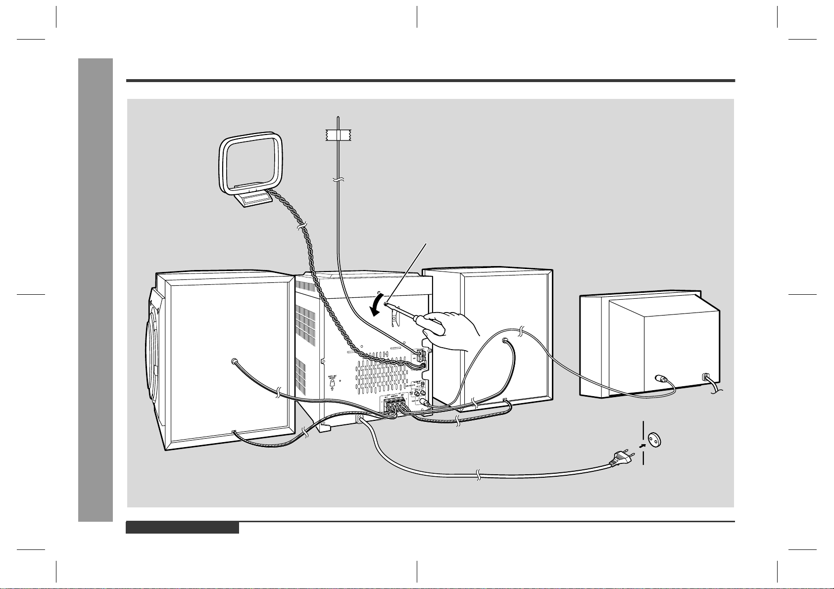
Rear panel
1.Transport screw
2. FM 75 Ohms Aerial Terminal
3. FM Aerial Earth Terminal
4. AM Loop Aerial Socket
5. Span Selector Switch
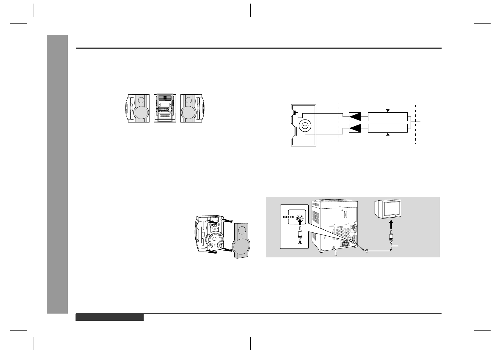
6. Video/Auxiliary (Audio Signal) Input Sockets
7. Video Output Socket
8. Speaker Terminals
9. AC Power Lead
10. AC Voltage Selector
10
4
5
3
2
1
8
6
9
7
Remo
t
te control
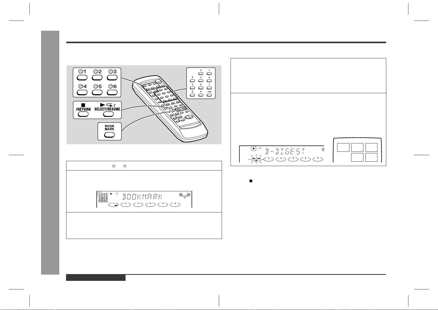
1. Remote Control Transmitter
2. Disc Direct Play Buttons
3. Echo Level Up and Down Buttons
4. Karaoke Mode Button
5. Video CD Auto/On Button
6. Video CD Playback Control Auto/Off Button
7. Video CD On Screen Display On/Off Button
8. Disc Clear Button
9. Video CD Digest/Time Search Button
10. Video CD Skip or Previous,
CD/MP3 Disc Track Down or Fast Reverse,
Tape 2 Fast Wind, Tuner Preset Down Button
11. Video CD Bookmark Button
12. Tape 2 Reverse Play Button
13. PAL/NTSC Select Button
14. Video CD/CD/MP3 Disc Button
15. Tape (1
2) Button
16. On/Stand-by Button
17. MP3 Disc Display Button
18. Disc Direct Search Buttons
19. Disc Random Button
20. Disc Memory Button
21. Video CD Skip or Next, CD/MP3 Disc Track Up or Fast Forward,
Tape 2 Fast Wind, Tuner Preset Up Button
22. Disc Pause Button
23. Video CD Play or Repeat or Select or Resume,
CD/MP3 Disc Play or Repeat, Tape 1 Play,
Tape 2 Forward Play Button
24. Video CD Stop or Return, CD/MP3 Disc/Tape Stop Button
25. Extra Bass Button
26. Equalizer Mode Select Button
27. Volume Up and Down Buttons
28. Tape 2 Record Pause Button
29. Tuner (Band) Button
30. Video/Auxiliary Button
Buttons with" " mark in the illustration can be operated on the remote control
only.
Other buttons can be operated both on the main unit and the remote control.
1
2
18
19
20
22
21
23
27
3
7
4
5
6
8
9
11
10
13
12
28
17
16
25
24
26
29
15
30
14
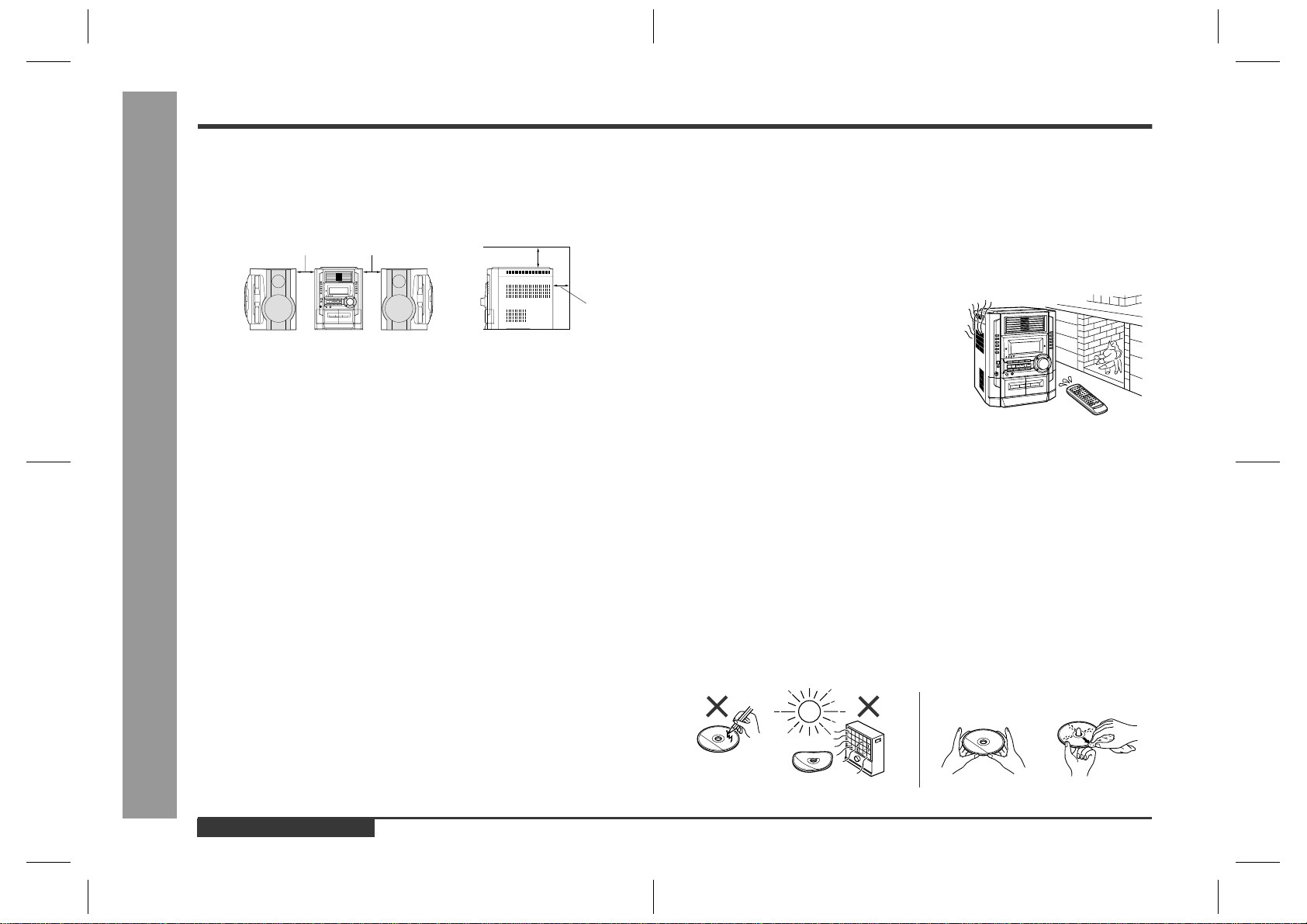
Transport screw
This product has a transport screw.
Be sure to drive it when transpoting the unit.
Before tuning the power on, be sure to remove the transport screw
on the back of the unit using a flat-blade screwdriver a coin.
CD-BK3200V
– 6 –
OPERATION MANUAL
CP-BK3200
1.Subwoofer
2.Bass Reflex Duct
3.Tweeter
4.Woofer
5.Speaker Wire for SUBWOOFER Terminals
6.Speaker Wire for MAIN Terminal
3
4
2
1
5
6
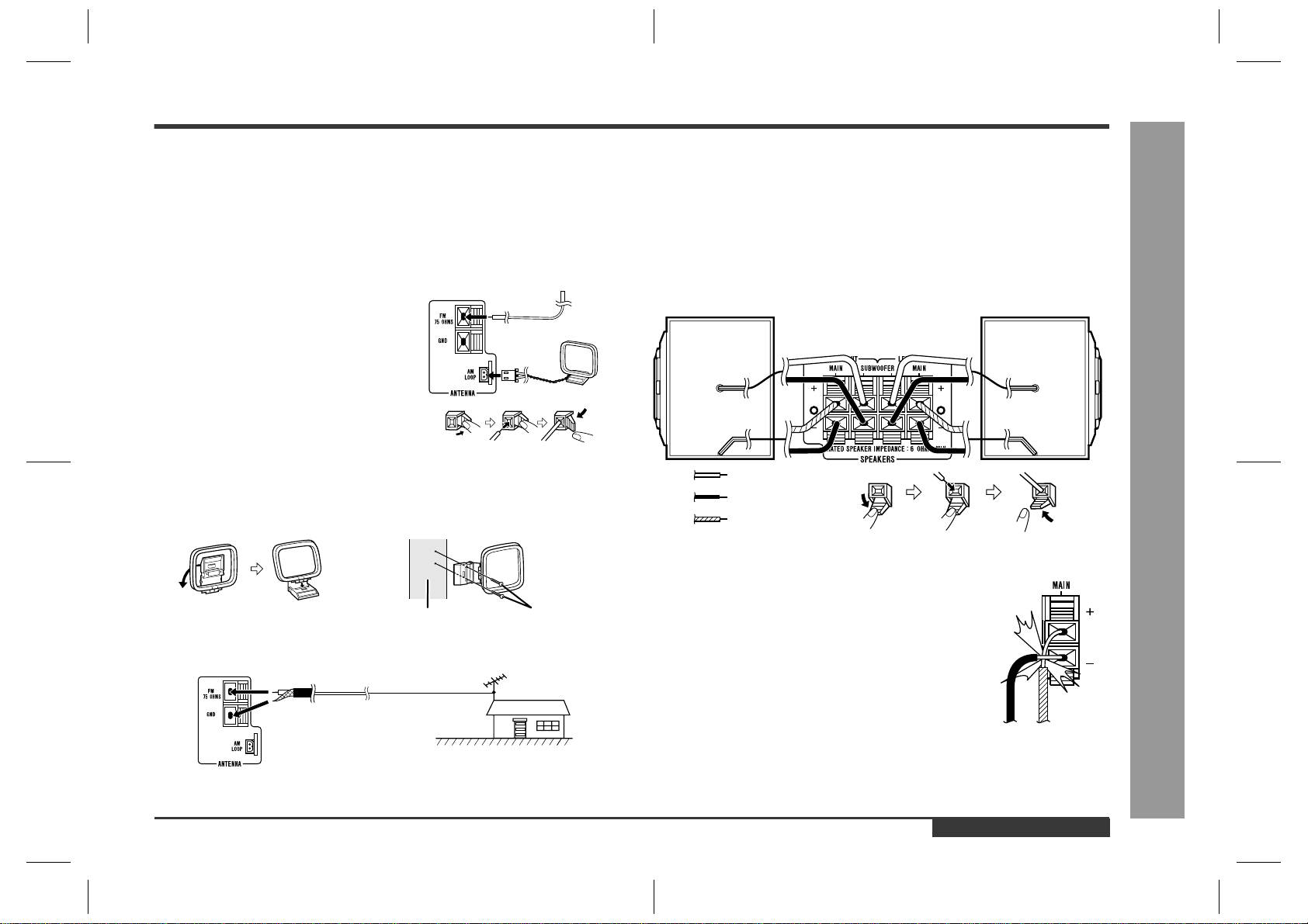
System Connections
Setting the AC voltage selector
Check the setting of the AC voltage selector located on the rear panel before plug-
ging the unit into a wall socket. If necessary, adjust the selector to correspond to the
AC power voltage used in your area.
Turn the selector with a screwdriver until the appropriate voltage num-
ber appears in the window (110 V, 127 V, 220 V or 230 V - 240 V AC).
Connecting the AC power lead
After making all connections, plug the unit. If you plug the unit first,
the unit will enter the demonstration mode.
Note:
Unplug the AC power lead from the wall socket if the unit will not be in use for a pro-
longed period of time.
AC Plug Adaptor
In areas (or countries) where a wall socket as shown in illustration is used, connect
the unit using the AC plug adaptor supplied with the unit, as illustrated. The AC plug
adaptor is not included in areas where the wall socket and AC power plug can be
directly connected (see illustration ).
Setting the FM/AM span selector
The International Telecommunication Union (ITU) has established that member coun-
tries should maintain either a 100 kHz or a 50 kHz interval between broadcasting fre-
quencies of FM stations and 10 kHz or 9 kHz for AM station. The illustration shows
the 50/9 kHz zones (regions 1 and 3), and the 100/10 kHz zone (region 2).
Before using the unit, set the SPAN SELECTOR switch (on the rear panel) to the
interval (span) of your area.
To change the tuning zone:
Caution:
This operation will erase all data stored in memory including clock, timer settings,
tuner preset, and CD programme.
1 Press the ON/STAND-BY button to enter the stand-by mode.
2 Set the SPAN SELECTOR switch (on the rear panel) as follows.
For 50 kHz FM interval (9 kHz in AM) 50/9
For 100 kHz FM interval (10 kHz in AM) 100/10
3 Whilst pressing down the MEMORY/SET button and the X-BASS/DEMO button,
press the ON/STAND-BY button until "CLEAR AL" appears.
1
2

– 7 –
CD-BK3200V
Setting the Clock
In this example, the clock is set for the 24-hour (0:00) display.
Note:
The "CLOCK" or time will flash at the push of the CLOCK button when the AC power
supply is restored after a power failure or unplugging the unit.
Readjust the clock as follows.
To readjust the clock:
Perform "Setting the Clock" from the beginning. If the time display is flashing, step 3
(for selecting the 24-hour or 12-hour display) will be skipped.
To change the 24-hour or 12-hour display:
1
Press the ON/STAND-BY button to turn the power on.
2
Press the CLOCK button and within 5 seconds, press the MEMO-
RY/SET button.
3
Press the TUNING/TIME ( or ) button to select 24-hour or 12-
hour display and then press the MEMORY/SET button.
"0:00" The 24-hour display will appear.
(0:00 - 23:59)
"AM 12:00" The 12-hour display will appear.
(AM 12:00 - PM 11:59)
"AM 0:00" The 12-hour display will appear.
(AM 0:00 - PM 11:59)
Note that this can only be set when the unit is first installed or it has been reset.
4
Press the TUNING/TIME ( or ) button to adjust the hour and then
press the MEMORY/SET button.
Press the TUNING/TIME ( or ) button once to advance the time by 1 hour.
Hold it down to advance continuously.
When the 12-hour display is selected, "AM" will change automatically to "PM".
5
Press the TUNING/TIME ( or ) button to adjust the minutes and
then press the MEMORY/SET button.
Press the TUNING/TIME ( or ) button once to advance the time by 1
minute. Hold it down to change the time in 5-minute intervals.
The hour will not advance even if minutes advance from "59" to "00".
The clock begins counting from "0" seconds. (Seconds are not displayed.)
The time display will disappear after a few seconds.
To confirm the time display:
Press the CLOCK button.
The time display will appear for about 5 seconds.
1 Clear all the programmed contents.
2 Perform "Setting the Clock" from the beginning.
Remote Control
Test of the remote control
Face the remote control directly to the remote sensor on the unit.
The remote control can be used within the range shown below:
Press the ON/STAND-BY button. Does the power turn on? Now, you can enjoy the
music.
0.2 m - 6 m
(8" - 20')
Remote sensor
CD-BK3200V
– 8 –
Troubleshooting Chart
Many potential problems can be resolved by the owner without calling a service tech-
nician.
If something is wrong with this product, check the following before calling your autho-
rised SHARP dealer or service centre.
General
Video CD
CD player
Tuner
Cassette deck
Karaoke
Remote control
Symptom Possible cause
The clock is not on time. Did a power failure occur? Reset the
clock.
When a button is pressed, the unit
does not respond.
Set this unit to the power stand-by mode
and then turn it back on.
If the unit still malfunctions, reset it.
No sound is heard. Is the volume level set to "0"?
Are the headphones connected?
Are the speaker wires disconnected?
Is the karaoke mode set to "L-CH", "R-CH"
or "V-CANCEL"?
Symptom Possible cause
The picture is not displayed during
playback.
Is the TV unplugged?
Is the unit connected improperly?
Is the input selector on the TV set to other
than "VCR"?
Is the unit being played without selecting
video CD?
The picture quality is poor, or it is
distorted.
Is the disc very dirty?
Symptom Possible cause
Playback does not start. Is the disc loaded upside down?
Playback stops in the middle or is
not performed properly.
Does the disc satisfy the standards?
Is the disc distorted or scratched?
Playback sounds are skipped, or
stopped in the middle of a track.
Is the unit located near excessive vibra-
tions?
Is the disc very dirty?
Has condensation formed inside the unit?
Symptom Possible cause
Radio makes unusual noise con-
secutively.
Is the unit placed near the TV or comput-
er?
Is the FM aerial or AM loop aerial placed
properly? Move the AC power lead away
from the aerial if located near.
Symptom Possible cause
Cannot record. Is the erase-prevention tab removed?
Cannot record tracks with proper
sound quality.
Is it a normal tape? (You cannot record on
a metal or CrO tape.)
Cannot erase completely.
Sound skipping. Is there any slack?
Is the tape stretched?
Cannot hear treble. Are the capstans, pinch rollers, or heads
dirty?
Sound fluctuation.
Cannot remove the tape. If a power failure occurs during playback,
the heads remain engaged with the tape.
Do not open the compartment forcibly.
Wait until electricity resumes.
Symptom Possible cause
The vocal part of a multiplexed
disc is not heard.
Is the karaoke mode set to "L-CH", "R-CH"
or "V-CANCEL"?
Symptom Possible cause
The remote control does not oper-
ate.
Is the AC power lead of the unit plugged
in?
Is the battery polarity respected?
Are the batteries dead?
Is the distance or angle incorrect?
Does the remote control sensor receive
stronglight?
If trouble occurs
When this product is subjected to strong external interference (mechanical shock,
excessive static electricity, abnormal supply voltage due to lightning, etc.) or if it is
operated incorrectly, it may malfunction.
If such a problem occurs, do the following:
1 Set the unit to the stand-by mode and turn the power on again.
2 If the unit is not restored in the previous operation, unplug and plug in the unit,
and then turn the power on.
Note:
If neither operation above restores the unit, clear all the memory by resetting it.
Clearing all the memory (reset)
1 Press the ON/STAND-BY button to enter the power stand-by mode.
2 Whilst pressing down the MEMORY/SET button and the X-BASS/DEMO button,
press the ON/STAND-BY button until "CLEAR AL" appears.
Caution:
This operation will erase all data stored in memory including clock, timer settings,
tuner preset, and CD programme.
Before transporting the unit
On the back of this unit is equipped with a transport screw in order to prevent damage
during transportation.
1 Press the ON/STAND-BY button to turn the
power on.
2 Remove all discs from the unit, close the
disc tray.
"NO DISC" is displayed.
3 Press the ON/STAND-BY button to enter the
stand-by mode.
"GOOD-BYE" is displayed.
4 When "GOOD-BYE" disappears, unplug the
AC power lead from the wall socket.
5 Insert the transport screw into the back of
the unit and tighten it with a flat-blade screw-
driver or a coin.
ions.
Troubleshooting Chart
– 9 –
CD-BK3200V
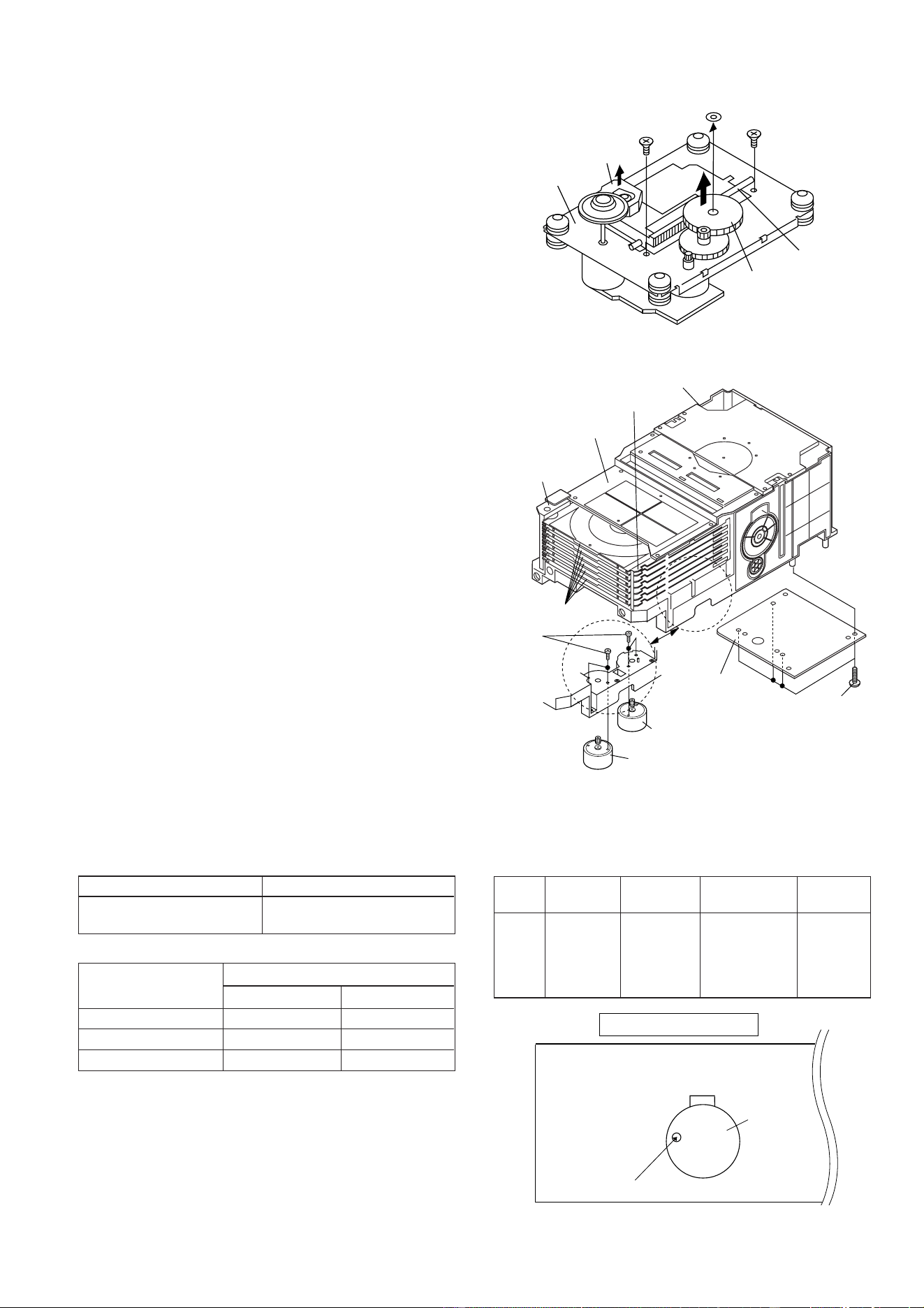
1 Top Cabinet 1. Screw ..................... (A1) x5 9-1
2 Side Panel 1. Screw .................... (B1) x10 9-1
(Left/Right) 2. Hook ....................... (B2) x2
3 Rear Panel with 1. Screw ..................... (C1) x2 9-2
Fan Motor 2. Screw ..................... (C2) x9
3. Screw ..................... (C3) x2
4. Socket .................... (C4) x1
4 CD Changer Unit 1. Socket .................... (D1) x4 9-2
2. Hook ....................... (D2) x2
5 Main PWB 1. Screw ..................... (E1) x1 9-2
2. Socket .................... (E2) x3 9-3
3. Flat Cable .............. (E3) x1
6 Power Amp. PWB 1. Screw ..................... (F1) x6 10-1
2. Socket .................... (F2) x4
9-3,10-1
3. Flat Wire................. (F3) x1 10-1
4. PWB Holder ........... (F4) x2
7 Front Panel 1. Screw ..................... (G1) x2 10-1
2. Hook ....................... (G2) x2
8 Eject Switch PWB 1. Screw ..................... (H1) x2 10-2
2. Socket .................... (H2) x1
9 Play Switch PWB 1. Screw ..................... (J1) x2 10-2
10 Display PWB 1. Knob ....................... (K1) x1 10-2
2. Screw ..................... (K2) x9
3. Flat Cable .............. (K3) x1
4. Hook ....................... (K4) x1
11 MIC PWB 1. Screw ..................... (L1) x1 10-2
2. Tip .......................... (L2) x1
12
Headphones PWB
1. Screw ..................... (M1) x1 10-2
2. PWB Washer ......... (M2) x1
13 Tape Mechanism 1. Open the cassette holder. 10-2
2. Screw ..................... (N1) x6
DISASSEMBLY
Caution on Disassembly
Follow the below-mentioned notes when disassembling
the unit and reassembling it, to keep it safe and ensure
excellent performance:
1. Take cassette tape and compact disc out of the unit.
2. Be sure to remove the power supply plug from the wall
outlet before starting to disassemble the unit.
3. Take off nylon bands or wire holders where they need to
be removed when disassembling the unit. After servicing
the unit, be sure to rearrange the leads where they were
before disassembling.
4. Take sufficient care on static electricity of integrated
circuits and other circuits when servicing.
Figure 9-2
Figure 9-3
STEP
REMOVAL
PROCEDURE
FIGURE
Figure 9-1
CD-BK3200V
CD-BK3200V
(B1) x 4
ø3 x 10mm
(B1) x 2
ø3 x 12mm
Rear
Panel
(B1) x 2
ø3 x 12mm
(B2) x 2
Side Panel
(Right)
Side Panel
(Left)
(A1) x 2
ø3 x 16mm
(A1) x 2
ø3 x 16mm
(B1) x 1
ø3 x 12mm
Top Cabinet
(B1) x 1
ø3 x 12mm
(A1) x 1
ø3 x 10mm
Main PWB
Main PWB
Power Amp.
PWB
Power B
PWB
(E3) x 1
Power A PWB
(F2) x 1
(F2) x 1
(E2) x 1
(E2) x 1
(E2) x 1
(E2) x 1
Tape
Mechanism
Mic
PWB
(D1) x 2
Video
CD PWB
Pull
(D2) x 1
(D2) x 1
CD Changer Unit
(D1) x 1
Video
CD PWB
(E1) x 1
ø3 x 10mm
Lug Wire
(C3) x 2
ø3 x 10mm
Main PWB
(C2) x 9
ø3 x 10mm
Power Amp.
PWB
(C4) x 1
(C1) x 2
ø3 x 10mm
Rear
Panel
(D1) x 1
Video
CD PWB
CD-BK3200V
– 10 –
Figure 10-1
Figure 10-2
Figure 10-3
1 Top Cabinet 1. Screw ................. (A1) x5 9-1
2 Side Panel 1. Screw ................(B1) x10 9-1
(Left/Right) 2. Hook .................. (B2) x2
3 Rear Panel with 1. Screw ................. (C1) x2 9-2
Fan Motor 2. Screw ................. (C2) x9
3. Screw ................. (C3) x2
4. Socket ................ (C4) x1
4 CD Changer Unit 1. Socket ................ (D1) x4 9-2
2. Hook ................... (D2) x2
5 Video CD PWB 1. Screw ................. (P1) x4 10-3
(Note) 2. Screw ................. (P2) x4
3. Socket ................ (P3) x4
4. Flat Wire ............. (P4) x2
6 CD Mechanism 1. Screw ................. (Q1) x4 10-3
STEP REMOVAL
PROCEDURE
FIGURE
CD-BK3200V (CD CHANGER MECHANISM UNIT)
Note:
After removing the connector for the optical pickup from the
connector, wrap the conductive aluminium foil around the
front end of connector remove to protect the optical pickup
from electrostatic damage.
Power Amp.
PWB
(F1) x 2
ø3 x 8mm
(F1) x 2
ø3 x 10mm
(F2)x1
(F2) x 1
Front Panel
(F4) x 1
(F1) x 1
ø3 x 10mm
(G1) x 2
ø3 x 8mm
Push
(F4) x 1
Push
(F1) x 1
ø3 x 10mm
Pull
(G2) x 1
Pull
(G2) x 1
Headphones
PWB
(F3) x 1
Push
Push
(K3) x 1
(K1) x 1
Display PWB
Play Switch
PWB
Open
Cassette
Holder
(H2) x 1
(N1) x 6
ø3 x 10mm
Tape
Mechanism
(H1) x 2
ø3 x 10mm
(J1) x 2
ø3 x 10mm
Eject Switch
PWB
Lug Wire
Headphones
PWB
Mic
PWB
(M1) x 1
ø3 x 10mm
(L1) x 1
ø3 x 10mm
(L2) x 1
(M2) x 1
(K2) x 9
ø3 x 10mm
(K4) x 1
(P2) x 4
ø3 x 10mm
(P1) x 4
ø3 x 14mm
(P4) x 1
(P3) x 1
(P3) x 1
(P4) x 1
(P3) x 2
Video CD
PWB
(Q1) x 4
ø2.6 x 10mm
CD Changer
Mechanism
Unit
CD Changer
Bracket
CD Mechanism
– 11 –
CD-BK3200V
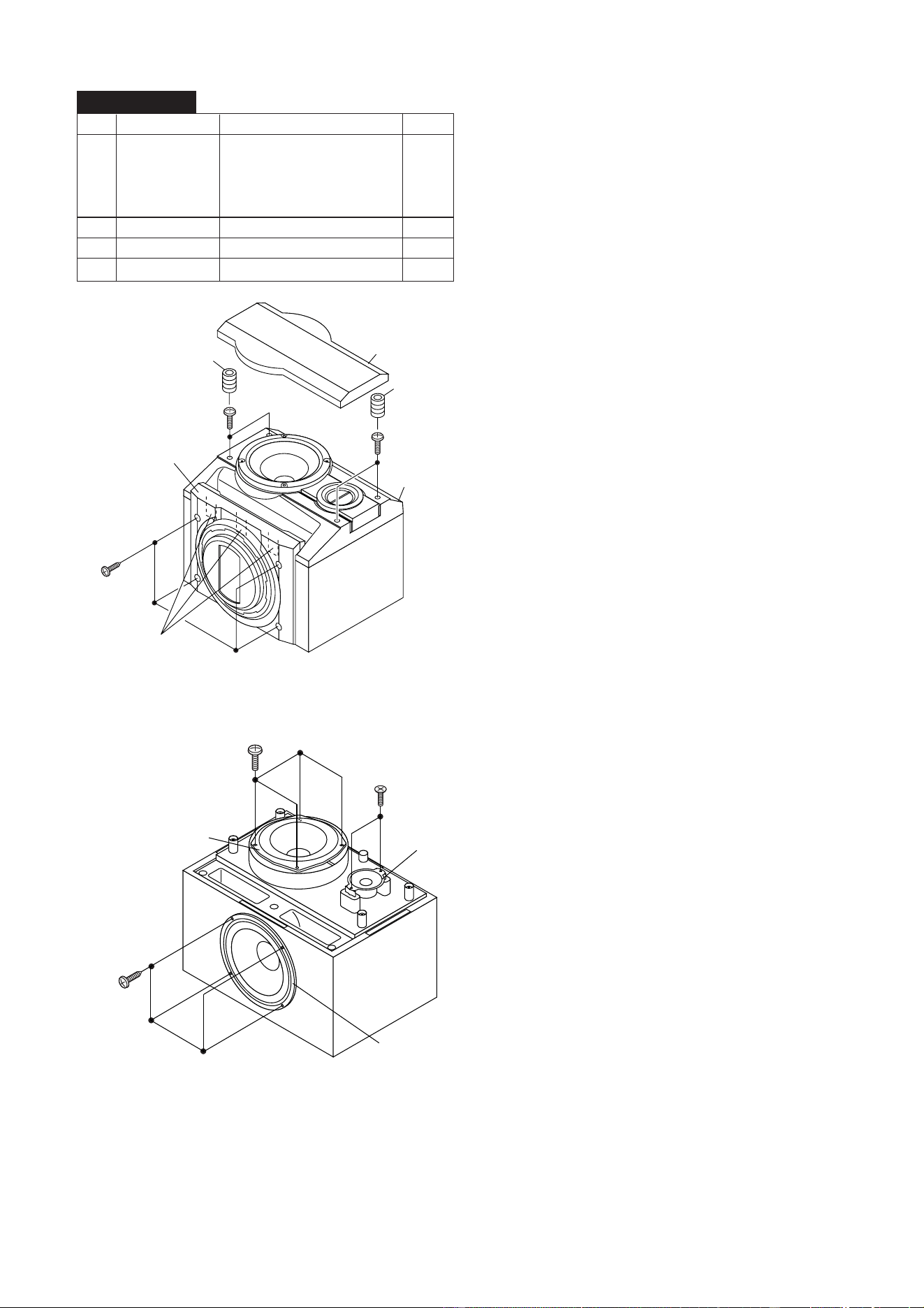
CP-BK3200
1 Side Panel/ 1. Screw ..................... (A1) x4 11-1
Front Panel 2. Hook ....................... (A2) x3
3. Net.......................... (A3) x1
4. Catching Holder ..... (A4) x4
5. Screw ..................... (A5) x4
2 Subwoofer 1. Screw ..................... (B1) x4 11-2
3 Woofer 1. Screw ..................... (C1) x4 11-2
4 Tweeter 1. Screw ..................... (D1) x2 11-2
STEP
REMOVAL PROCEDURE
FIGURE
Figure 11-1
(A1) x 4
ø4 x 20mm
(A5) x 2
ø4 x 20mm
(A4) x 2
(A4) x 2
Fromt Panel
Side Panel
(A3) x 1
(A5) x 2
ø4 x 20mm
(A2) x 3
(C1) x 4
ø4 x 16mm
(B1) x 4
ø4 x 16mm
(D1) x 2
ø3 x 10mm
Tweeter
Woofer
Subwoofer
Figure 11-2
CD-BK3200V
– 12 –
REMOVING AND REINSTALLING THE MAIN PARTS
TAPE MECHANISM SECTION
Perform steps 1 to 4 and 7, 13 of the disassembly method to
remove the tape mechanism. (See page 9.)
How to remove the record/playback and erase
heads (TAPE 2) (See Fig. 12-1)
1. When you remove the screws (A1) x 2 pcs., the recording/
playback head and three-dimensional head of the erasing
head can be removed.
How to remove the playback head (TAPE 1)
(See Fig. 12-2)
1. When you remove the screws (B1) x 2 pcs., the playback
head.
How to remove the pinch roller (TAPE 1/2)
(See Fig. 12-3)
1. Carefully bend the pinch roller pawl in the direction of the
arrow <A>, and remove the pinch roller (C1) x 1 pc., in the
direction of the arrow <B>.
Note:
When installing the pinch roller, pay attention to the spring
mounting position.
How to remove the belt (TAPE 2) (See Fig. 12-4)
1. Remove the main belt (D1) x 1 pc., from the motor side.
2. Remove the FF/REW belt (D2) x 1 pc.
How to remove the belt (TAPE 1) (See Fig. 12-4)
1. Remove the main belt (E1) x 1 pc., from the motor side.
2. Remove the FF/REW belt (E2) x 1 pc.
How to remove the motor (See Fig. 12-5)
1. Remove the screws (F1) x 2 pcs., to remove the motor.
Figure 12-1
Figure 12-2
Figure 12-3
Figure 12-4Figure 12-5
(A1) x 2
Ø2 x 6mm
TAPE 2
Record/Playback
Head
Erase Head
Clutch Ass'y
(B1) x 1
Ø2 x 9mm
(B1) x 1
Ø2 x 5mm
TAPE 1
Playback
Head
Clutch Ass'y
Pinch Roller
(C1) x 1
<A>
Pull
<B>
Pull
Pinch
Roller
Pawl
TAPE 2
TAPE 1
Main Belt
(E1) x 1
TAPE 2
Main Belt
(D1) x 1
TAPE 1
FF/REW
Belt
(D2) x 1
FF/REW
Belt
(E2) x 1
Tape
Motor
Tape
Motor
Main Belt
(D1) x 1
Main Belt
(E1) x 1
FF/REW
Roller
FF/REW
Roller
Flywheel
Ass'y
Flywheel
Ass'y
(F1) x 2
Ø2.6 x 5mm
Tape
Motor
Clutch Ass'y
– 13 –
CD-BK3200V
Figure 13-2
Figure 13-1
ADJUSTMENT
MECHANISM SECTION
• Driving Force Check
Torque Meter Specified Value
Play: TW-2111 Tape 1: Over 80 g
Tape 2: Over 80 g
• Torque Check
Torque Meter
Tape 2
Play: TW-2111 30 to 80 g.cm 30 to 80 g.cm
Fast forward: TW-2231 — 70 to 180 g.cm
Rewind: TW-2231 — 70 to 180 g.cm
Specified Value
Tape 1
Specified
Value
Adjusting
Point
Instrument
Connection
Test Tape
Normal MTT-111 Variable 3,000 ± 30 Hz Speaker
speed Resistor in Terminal
motor. (Load
resistance:
6 ohms)
• Tape Speed
Figure 13-3
TAPE MECHANISM
Tape
Motor
Variable Resistor in motor
(A1) x 1
ø2.6 x 6mm
CD
Mechanism
Stop Washer
(A3) x 1
Gear
(A4) x 1
Shaft
(A2) x 1
Pickup
(A1) x 1
ø2.6 x 6mm
Main Cam Motor
Tray Motor
Video
CD PWB
(1)Front Top Plate
(2)Changer Box,
Left
(2)Changer Box,
Right
(3)Disc Tray,1~6
CD Changer Mechanism
(B1) x 4
ø3 x 10mm
(B2) x 4
ø2.6 x 4mm
CD MECHANISM SECTION
Perform steps 1 to 6 of the disassembly method to remove the
CD mechanism. (See page 10.)
Note:
After removing the connector for the optical pickup from the
connector, wrap the conductive aluminium foil around the
front end of connector remove to protect the optical pickup
from electrostatic damage.
How to Remove the pickup (See Fig. 13-1)
1. Remove the screws (A1)x 2 pcs., to remove shaft (A2)x 1
pc.
2. Remove stop washer (A3)x 1 pc., to remove gear (A4)x 1 pc.
3. Remove the pickup.
How to Remove the tray motor/main cam motor
(See Fig. 13-2)
1. Remove the screws (B1)x 4 pcs., to remove the CD Servo
PWB.
2. Remove the (1) front top plate, (2) changer box, left/right
and (3) disc trays 1~6. After that, disassemble as shown in
the figure.
3. Remove the screws (B2)x 4 pcs.
4. Remove the tray motor and main cam motor.
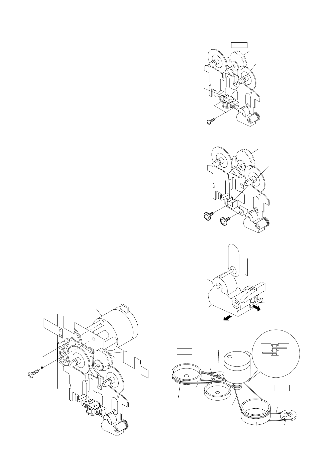
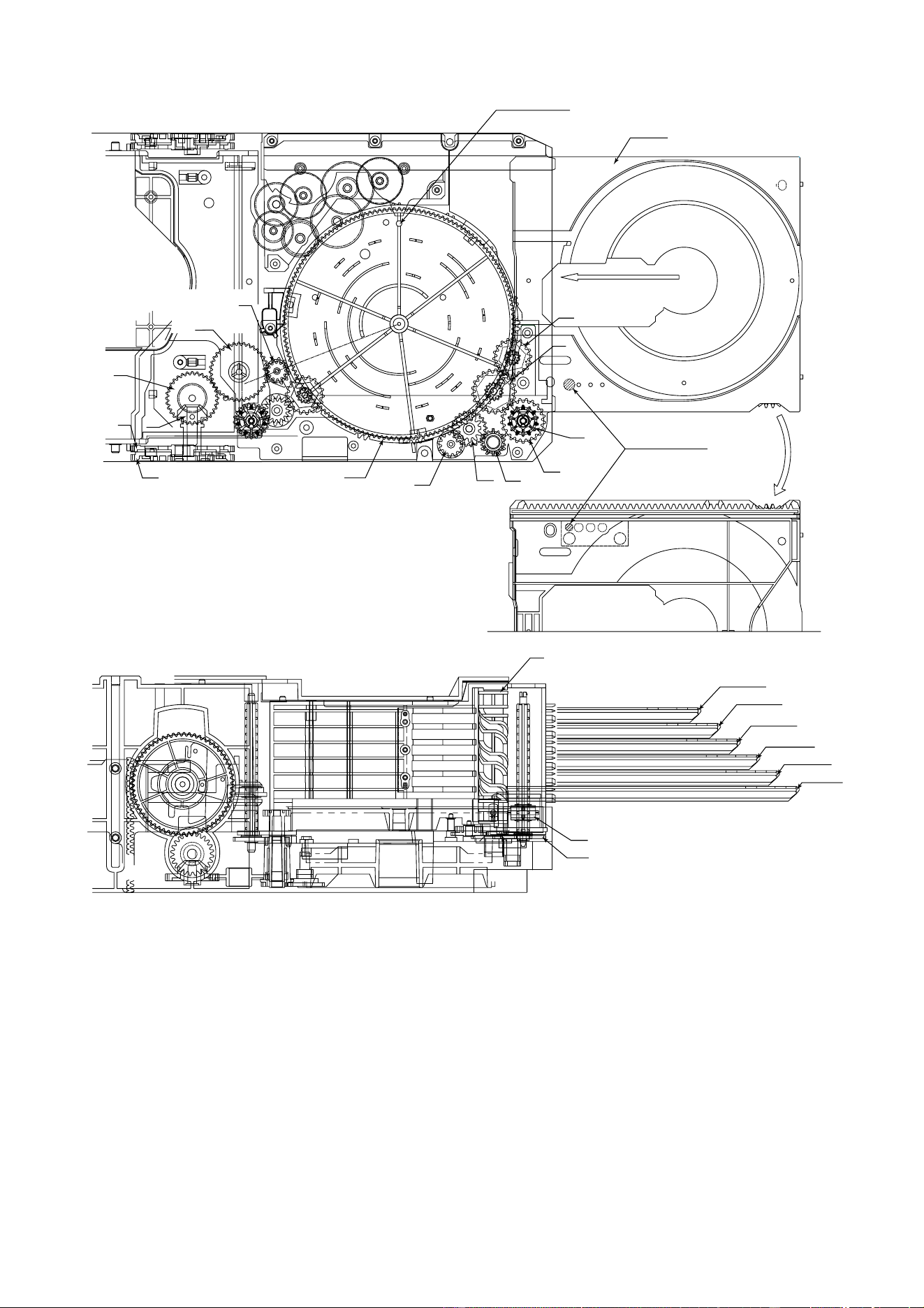
CD CHANGER MECHANISM SECTION
Perform steps 1 to 4 of the disassembly method to remove the
CD changer mechanism. (See page 10.)
Note:
The parts of (1), (2) and (3) correspond to the drawing Nos.
117, 102, 103 and 108 to 113 of the CD change mechanism
disassembly drawing.
Remove the screws of 117, 102 and 103, and the parts of (1),
(2) and (3) will be ready for removal and the screws of the tray
motor and main cam motor will be visible.
CD-BK3200V
– 14 –
CD SECTION
Figure 14-2
CD ERROR CODE DESCRIPTION
Error State Code
[Pickup Mechanism Error]
ER-CD00 Pickup mechanism error
ER-CD01 Pu-in SW detection NG
[CD Changer Mechanism Error]
ER-CD10 Changer error
ER-CD11 Initial error
ER-CD20 Tray error
Items adjusted automatically
(1) Offset adjustment (The offset voltage between the head
amplifier output and the VREF reference voltage is
compensated inside the IC.)
* Focus offset adjustment
* Tracking offset adjustment
(2) Tracking balance adjustment (waveform drawing
Fig.14-2 EFBL)
(3) Gain adjustment (The gain is compensated inside the IC
so that the loop gain at the gain crossover frequency will
be 0 dB.)
* Focus gain adjustment
* Tracking gain adjustment
• Adjustment
Since this CD system incorporates the following automatic
adjustment functions, readjustment is not needed when
replacing the pickup. Therefore, different PWBs and pickups
can be combined freely.
Each time a disc is changed, these adjustments are
performed automatically. Therefore, playback of each disc
can be performed under optimum conditions.
T
T
EFBL
FDO
TE
Stopped
CH1=500mV
DC 10:1
CH2=200mV
DC 10:1
CH3=1V
DC 10:1
500ms/div
(500ms/div)
NORM:20kS/s
1
2
3
=Record Length=
Smoothing : ON CH1 : 0.000V
CH2 : 0.000V
Main : 100K
Zoom : 2k
Mode : SINGLE
Type : EDGE CH1
Delay : 0.0ns
Hold off : 0.2µs
CH3 : 0.00V
CH4 : 0.00V
BW : FULL
=Trigger==Filter= =Offset=
CH2
v/DIV
200mV
1999/04/05 20:26:47
Test Stage
Frequency Frequency
Display
Setting/
Adjusting
Parts
Instrument
Connection
• AM IF/RF
Signal generator: 400 Hz, 30%, AM modulated
*1. Input: Antenna Output: TP302
*2. Input: Antenna Output: TP301
TUNER SECTION
fL: Low-range frequency
fH: High-range frequency
AM IF 450 kHz 1,602 kHz T351 *1
AM Band — 531 kHz (fL): T306 *2
Coverage 1.1 ± 0.1 V
AM Tracking 990 kHz 990 kHz (fL): T303 *1
*1. Input: Antenna Output: TP301
*2. Input: Antenna Output: Speaker terminal
• FM RF
Signal generator: 1 kHz, 40 kHz dev., FM modulated
FM Band — 88.00 MHz T301(fL): *1
Coverage
1.3 V ± 50 mV
FM RF 98.00 MHz 98.00 MHz L312 *2
(10-30 dB)
Test Stage
Instrument
Connection
Frequency Frequency
Display
Setting/
Adjusting
Point
IC301
AM IF
FM IF
FM RF
T303
T306
T302
L312
AM
TRACKING fL
AM BAND
COVERAGE fL
T301
T351
FM BAND
COVERAGE fL
MAIN PWB
CNP301
AM LOOP
ANTENNA
SO302
FM ANTENNA
TERMINAL
TP302
R357
R316
TP301
Figure 14-1 ADJUSTMENT POINTS
– 15 –
CD-BK3200V
TEST MODE
During POWER OFF mode, push below each 2 keys and [POWER] key. Then go to each Test Mode.
KEY TEST MODE CONTENTS
[CD] [X-BASS] + [POWER] TEST 1 CD Test mode
[TAPE] [X-BASS] + [POWER] TEST 2 Tape test mode
[TUNER] [X-BASS] + [POWER] TEST 3 Tuner preset memory clear
[VIDEO/AUX] [X-BASS] + [POWER] TEST 4 Tuner preset for production
[MEMORY/SET] [X-BASS] + [POWER] TEST 5 All clear (reset)
[EQUALIZER] [X-BASS] + [POWER] TEST 6 Audio test
[ ] [DIMMER] + [POWER] TEST 7 Key and display test
[TUN UP] [DIMMER] + [POWER] TEST 8 RDS Test1
[TUN DOWN] [DIMMER] + [POWER] TEST 9 RDS Test2
[ ] [CD] + [POWER] TEST 10 CD Changer test
[ ] [CD] + [POWER] TEST 11 Production initialize for changer
[EQUALIZER] [TUN UP] + [POWER] TEST 12 Graphic equalizer test
CD TEST MODE
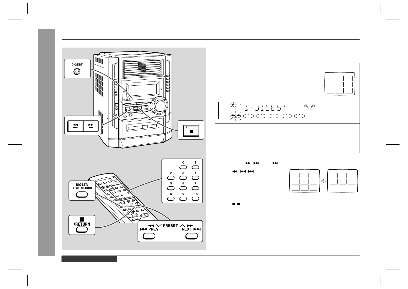
· Setting the test mode
Any one of test mode can be set by pressing several keys as follows.
<X-BASS> + <CD> + <POWER> TEST: CD operation test
Enter test 1 mode key.
C D T E S T
OPEN/CLOSE operation is using manual.
Do TOC IL. Do normal play.
When these following key is input into PLAY key,
track number can be appoint directly.
<<PLAY>> key input.
<<MEMORY>> key input.
Laser ON.
<<MEMORY>> key input.
Tracking OFF play at that specific point.
<<MEMORY>> key input.
<< 1>> key: Track 1
<< 2>> key: Track 3
<< 3>> key: Track 7
<<
4>> key: Track 11
<< 5>> key: Track 13
<< 6>> key: Track 15
Tracking ON play from that specific point.
<<MEMORY>> key input
a) Display "FOF_XXXX"
b) Display "TOF_XXXX"
c) Display "TBA_XXXX"
d) Display "TGA_XXXX"
e) Display "FGA_XXXX"
f) Display "RFL_XXXX"
<<
>>, << >> buttons make pick's slide possible.
<<STOP>> key input.
STOP
<<MEMORY>> key input.
a) Display "FOF_XXXX"
b) Display "TOF_XXXX"
c) Display "TBA_XXXX"
d) Display "TGA_XXXX"
e) Display "FGA_XXXX"
f) Display "RFL_XXXX"
Display every auto setting result for every 2 sec.
<<STOP>> key input.
STOP
VOL –– Last memory
BAL –– CENTER
P.GEQ –– FLAT
X-BASS –– OFF
Sliding the PICKUP with
<<
>>, << >> button
must only be in STOP mode.
Display each step for 2 sec. XX: HEX VALUE
a) "FOF_XXXX" Focus off set
b) "TOF_XXXX" Tracking off set
c) "TBA_XXXX" Tracking balance
d) "TGA_XXXX" Tracking gain
e) "FGA_XXXX" Focus gain
f ) "RFL_XXXX" RF level shift
To cancel : Power OFF
CD-BK3200V
– 16 –
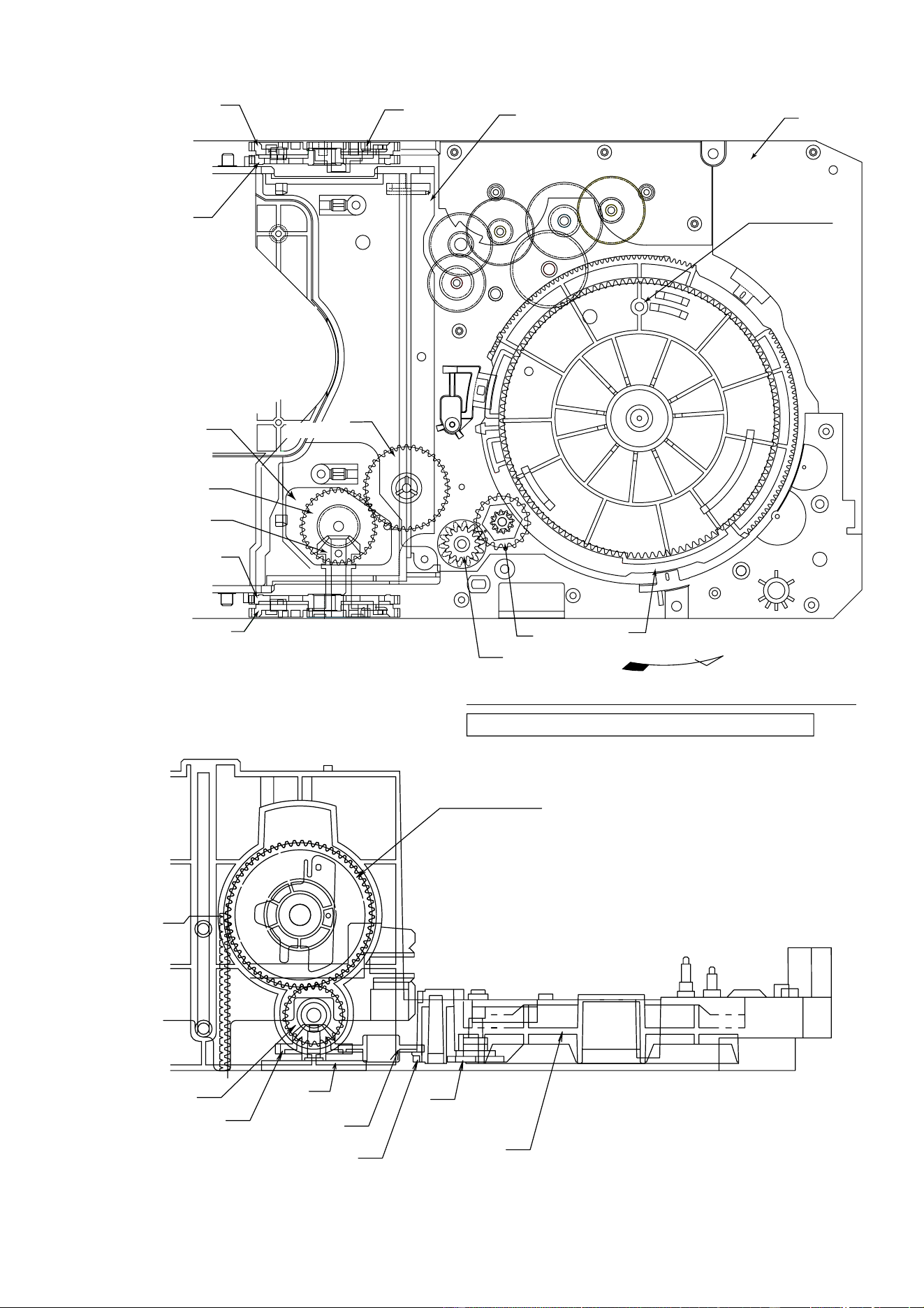
1. Motor assembly (x 2) mounting (screw x 4) 01/29 Fig.17
2. MT idle gear mounting (screw x 1) 25 Fig.17
3. MT system gear assembly 23/24/26/27 Fig.17
4. STB/tray drive system gear and others assembling/ 37/38/45/46 (53)/47/48 Fig.17
mounting (screw x 3)
5. Tray big gear assembly 31 Fig.17 Gear positioning
6. T.M SW PWB mounting (screw x 3) Fig.18
7. STB holder assembling 03 Fig.17
8. STB drive gear L/R assembly mounting (screw x 2) 11 (10)/12 (10) Fig.17
9. Tray joint gear R/tray drive gear R assembling 34/36 Fig.18 Gear positioning
10. Tray gear A/B assembling 32/33 Fig.18 Gear positioning
11. Lift gear B/C assembling 43/44 Fig.19 Gear positioning
12. MT idler gear F assembling, mode big gear 28/42 Fig.19
mounting (screw x 1)
13. Change box R mounting (screw x 4) 04 Fig.19
14. Lift gear A assembling 42 Fig.19 Gear positioning
15. Change box L assembly mounting (screw x 4) 02/30/35 Fig.20
16. Lift cam assembling (shaft inserting) 44 Fig.20 Gear positioning
17. STB holder height adjusting Fig.21 Check/adjustment
18. Top plate F/disc OB LEV. Mounting (screw x 6) 80 Fig.21
19. Trays 1 - 6 assembling 91/92/93/94/95/96 Fig.22
20. Top plate R mounting (screw x 6) ––
Applied Part No.
Work Content
Assembly Fig. No.
Remarks
CD CHANGER MECHANISM MAIN BASE PARTS ASSEMBLING/ADJUSTING
PROCEDURE
01 (101) MAIN BASE
02 (102) CHANGE BOX L
03 (147) STB HOLDER
04 (103) CHANGE BOX R
10 (119) STB DRIVE GEAR A
11 (120) STB DRIVE GEAR L
12 (122) STB DRIVE GEAR R
20 (149) STABILIZER FH
23 (141) MT IDLER GEAR A
24 (138) MT IDLER GEAR B
25 (137) MT IDLER GEAR C
26 (140) MT IDLER GEAR D
27 (139) MT IDLER GEAR E
28 (131) MT IDLER GEAR F
29 (MOB1,2) MOTOR GEAR
30 (143) TRAY DRIVE GEAR F
31 (134) TRAY BIG GEAR
32 (135) TRAY GEAR A
33 (136) TRAY GEAR B
34 (124) TRAY DRIVE GEAR R
35 (144) TRAY JOINT GEAR F
36 (125) TRAY JOINT GEAR R
37 (142) TRAY GEAR C
38 (130) TRAY IDLER GEAR
Part Name
No.
40 (115) LIFT CAM
41 (126) MODE BIG GEAR
42 (127) LIFT GEAR A
43 (128) LIFT GEAR B
44 (129) LIFT GEAR C
45 (132) STB GEAR A
46 (104) STB GEAR B
47 (133-1) STB GEAR C
48 (133-3) STB GEAR D
50 (145) LIFT LEVER
51 (106) TRAY LOCK LEVER
52 (118) DISC OB LEVER
53 (105) STB GEAR ANG.
80 (117) TOP PLATE F
81 (114) TOP PLATE R
91 (108) TRAY 1
92 (109) TRAY 2
93 (110) TRAY 3
94 (111) TRAY 4
95 (112) TRAY 5
96 (113) TRAY 6
Part Name
No.
CD CHANGER MECHANISM PARTS LIST
The number of ( ) is the number of the parts guide.
– 17 –
CD-BK3200V
Figure 17
03
STB HOLDER
48
STB GEAR D
12
STB DRIVE GEAR R
(ASSY)
10
STB DRIVE GEAR A
29
29
23
23
24
25
26
27
01
MAIN BASE
Mark position
After assembling TRAY BIG GEAR, turn it in the arrow direction.
TRAY BIG GEAR ASSEMBLING POSITION
31
TRAY BIG GEAR
37
TRAY GEAR C
38
TRAY IDLER GEAR
47
STB GEAR C
46
STB GEAR B
10
STB DRIVE GEAR A
11
STB DRIVE GEAR L
(ASSY)
53
STB GEAR ANG.
45
STB GEAR A
11(/12) (10)
STB DRIVE GEAR L(/R)
(ASS'Y)
46
STB GEAR B
37
TRAY GEAR C
47
STB GEAR C
31
TRAY BIG GEAR
38
TRAY IDLER GEAR
45
STB GEAR A
53
STB GEAR ANG.
L
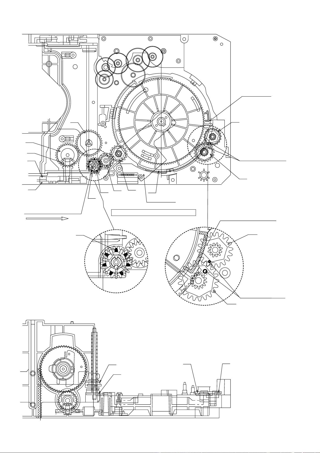
CD-BK3200V
– 18 –
31
M T SW PWB
33
TRAY
GEAR B
32
TRAY GEAR A
33
TRAY GEAR B
37
32
TRAY GEAR A
38
34
TRAY DRIVE GEAR R
36
TRAY JOINT GEAR R
47
46
34
TRAY DRIVE GEAR R
36
TRAY JOINT GEAR R
10
29
29
23
23
24
25
26
27
Mark position
11
45
TRAY BIG GEAR SET POSITION
33
32
Direct the recess part
(trapezoidal side) of the axis
35 in this direction.
* This position becomes the
reference (stock) position
of the tray.
These holes must align.
It must not rotate in contact
with the peripheral (hatched)
part of 31.
These holes must align.
After assembling 32,
assemble 33.
*1: To position the axis part of 36, engage it with 38.
*2: When it is aligned as described in *1, the hatched part
(low gear-height part of gear) will be positioned in this position.
Note: After positioning the tray big gear in the set position, engage these gears.
*1
*2
Scale: 2 magnifications
Scale: 2 magnifications
LL
< Importance >
< Importance >
Figure 18
– 19 –
CD-BK3200V
43
LIFT GEAR B
41
MODE BIG GEAR
04
CHANGE BOX R
47
46
28
MT IDLER GEAR F
10
Mark position
(Assemble the mode big gear in this position.)
11
45
42
LIFT GEAR A
37
38
44
LIFT GEAR C
34
36
(A)
(C)
(B)
44
LIFT GEAR C
43
LIFT GEAR B
42
LIFT GEAR A
41
MODE BIG GEAR
Note:
To assemble the mode
big gear, incline it,
bring it into contact with
the circumference and
put the center hole into
position since the
hatched part of the main
base is overlapped with
the circumference.
Direct the short tooth
toward the center.
MODE BIG GEAR
LIFT GEAR A/B/C
ASSEMBLING POSITION
Scale: 2 magnifications
Scale: 2 magnifications
<Assembling method of lift gear>
After setting up the mode big gear in the
shown position, engage it with the STB gear A
(gear on the lower side) at the position (A),
and assemble them, turning it in the arrow direction
into the position (B). (The short tooth directs toward the
center of the mode big gear.)
Check the gap (C) after assembly.
If no gap is found, repeat the above procedure.
L
C1
>ABS<
GAP (0.3-1.5 mm)
33
32
< Importance >
< Importance >
Figure 19
CD-BK3200V
– 20 –
Mark position
37°
33
32
30
TRAY DRIVE GEAR F
35
TRAY JOINT GEAR F
02
CHANGE BOX L
< Importance >
Direct the recess part
(trapezoidal side) of the
axis 35 in this direction.
*2
*1: To position the axis part
of 35, engage it with 33.
*2: When it is aligned as
described in *1, the hatched part
(low gear-height part of gear)
will be positioned as shown.
Since this gear engagement is not
visually checked, verify that it does
not float when the gear box L is installed.
30
TRAY DRIVE GEAR F
35
TRAY JOINT GEAR F
*1
43
41
40
LIFT
CAM
Scale: 2 magnifications
44
11
TRAY JOINT GEAR F
(CHANGE BOX L ASS'Y) ASSEMBLING POSITION
LIFT CAM
Assembling procedure
1. Turn the mode big gear approx. 37 degrees in the arrow direction.
2. Assemble the change box L ass'y.
Note: At this time, the tray joint gear F must be located in the position shown in figure.
Moreover, the gear must be engaged securely.
3. After assembly, return the mode big gear to the initial position.
4. Assemble the lift cam.
Note: At this time, the lift cam (No.40) must be located in the position shown in figure 20.
47
46
10
45
42
LIFT GEAR A
28
L
40
LIFT CAM
Scale: 2 magnifications
During assembly, make the
O part visible in this direction.
Note: Among 4 ribs on the
circumference, one rib alone
is provided with O.
< Importance >
30
TRAY DRIVE GEAR F
35
TRAY JOINT GEAR F
Figure 20
– 21 –
CD-BK3200V
Figure 21
Adjusting procedure
1. Turn the mode big gear approx. 37 degrees in the arrow direction.
2. Viewing from the front side of the mechanism, verify that the guide ribs
(CHANGE BOX L/R and STB HOLDER)of tray are as tall as each other.
3. If they are not, bend the lever for adjustment. (Refer to the details.)
Note: Also apply the same adjustment on the R side.
STB HOLDER HEIGHT ADJUSTING METHOD
47
46
10
11
45
42
LIFT GEAR A
43
41
32
35
40
44
33
30
Mark position
80
TOP PLATE F
37°
(121)
OS LEVER
Bend this portion to adjust the STB HOLDER
When high
(Narrow the gap.)
When low
(Broaden the gap.)
Adjustment procedure
1. Rotate the MODE BIG GEAR by 37° in the arrowed direction.
2. Check that the guide ribs (CHANGE BOX L/R and STB HOLDER) on the arrowed
TRAY are at the same height when looked from the front.
3. If they are not, bend the OS LEVER to adjust them. (Refer to the detail drawing.)
Note: Adjust the R portion in the same procedure.
02(102) CHANGE BOX L RIB
03(147) STB HOLDER RIB
03(147) STB HOLDER RIB
04(103) CHANGE BOX R RIB
CD-BK3200V
– 22 –
Measure to be taken when a disc cannot be removed due to a mechanism trouble
First, remove the mechanism unit section from the set, and check for the state of the disc.
(Remove the top plate R if necessary.)
<State of the disc>
(1) When the disc is in the normal PLAY (chucking) position → Try to eject the disc by turning the mode big gear/tray big gear
manually.
* At this time, be sure to adjust the tray's position (height).
(2) When the disc is in the normal STOCK position → Try to eject the disc by turning the tray big gear manually.
* At this time, be sure to adjust the tray's position (height).
(3) When the disc is not in the normal position → The tray or disc is not in the normal position.
(The tray or disc may catch somewhere.)
↓
Remove the TOP PLATE F/DISC OB lever.
Unlock the tray lock lever and pull out the tray which is not caught.
Move the caught tray or disc and remove the disc.
In case of (1) and (2), the mechanism is normal (defective circuit parts, etc.). However, it may stop somewhere.
This is the reason why you should try to turn the tray big gear first.
In case of (3), either of the big gears does not turn.
Figure 22
L
91~96
TRAY1~TRAY6
Mark position
Be sure to assemble the tray into this position.
32
Insert it along the guide of
the change box.
Rear
side
33
30
35
TRAY No.1~6
Rear surface: Stamped.
Note: During insertion,
Do not accidentally rearrange
tray numbers.
43
41
40
44
47
46
10
11
Tray installing method: (After adjusting the height of the STB holder)
1. Turn the mode big gear to the mark position to lower the STB holder to
the bottom area.
2. From the front side, install the tray. (Securely insert it to the lock position.)
TRAY 6
TRAY 5
TRAY 4
TRAY 3
TRAY 2
TRAY 1
40
30
35
42
LIFT GEAR A
45

– 23 –
CD-BK3200V
Track 2 Video output terminal
Chroma Peak Level
105 ± 15 IRE
VIDEO CD SECTION
TEST DISC Model No.TVD-581A (NTSC/PAL)
• Checking of video output signal
Checking of color bar
Disc Adjusting Point
Instrument
Connection
Figure 23-1 CHECKING OF VIDEO OUTPUT SIGNAL
Figure 23-2
UNIT
Video Output Terminal
Video Input Terminal
TV
Color bar signal
waveform
100 100
88.5
75
70
75
41.5
33.5
5
0
-13.5
-25 -25
100 IRE
(0.714 V)
(1 V)
(0.286 V)
140 IRE
Horizontal
sync signal
40 IRE
40 IRE
Color Burst
20
-20
-40
Blue
Red
Green
Magenta
Cyan
Yellow
Gray
(59.94 Hz)
IH
Figure 23-3
TV monitor
Blue
Red
Green
Magenta
Cyan
Yellow
Gray
Set the phase of color
Phase check
Track 2 VIDEO OUT burst signal (B) to
±10°
180° -360° line.
Disc Checking Setting
Checking
Item
Checking of vector scope waveform
( Check that the setting is within the illustrated range.)
Figure 23-4
90
80
70
60
50
40
30
20
10
360
350
340
330
320
310
300
290
280
270
260
250
240
230
220
210
200
190
180
170
160
150
140
130
120
110
100
103.4
167.1
240.8
283.4
347.1
60.8
-1
123 +180
+0
33
MG
R
BL
CY
G
YE
Vector scope waveform of color bar signal
Figure 23-5
TV monitor
Blue
Red
Green
Magenta
Cyan
Yellow
Gray
CD-BK3200V
– 24 –
Figure 24-1
Track 3 VIDEO OUT 150 line.
Output level
±10 IRE
Disc Checking Setting
Checking
Item
Checking the black-and-white level
Figure 24-2
IRE
100
80
60
40
20
-20
-40
100%
12.5%
0%
NTSC
Waveform on 140 LINE
(This burst level
is 40 IRE)
140 IRE
TV monitor

– 25 –
CD-BK3200V
Figure 25 BLOCK DIAGRAM (1/3)
IC6
BA4558F
OPE AMP.
7
6
5
3 2 1
CNP3
CNP10
CNP6
CNP5
CNP4
90
89 8680
79787366
6462 57 56 51 4341
3733
3126 25
23
6
1
100
95 94 93 87 82
8050474544434132 30
CNP7
CNP8
75
7271 70 69 68 67 66655251
333226252423
40
35
29
28
24
23
22
21
18
14
8
302311
9
1
20
2
5
6
10
16
19
40
35
21
39
36
34
31
26
22
62
55
79
68
66
65
64
1
31
81
13
4
12
28
51
32
30
17
15
22
24
13
2
1
12
25
23
21
16
15
27
26
4
5
6
7
42
1
2
17
25
37
36
39
41
38
93
48
99
95
47
45
46
98
92
8
81
63
72
75
91
77
100
5
16
32
53
59
60
17
18
19
20
21
22
7
8
4
3
2
1
8
4
46
53
47
41
31
30
40
19
3
15
16
14
7
49
44
36
18
5
73
50
AOR–
AOR+
AOL+
AOL–
F
E
F
E
AOL+
AOL–
AOR–
AOR+
VGND
NSW1
PICKUP
IN
NM2
SLED
NM3
SPINDLE
VDAC
TO MAIN
SECTION
VDAC
CAMA_E_B_A
CAMA_A_B
CAMA_C_D
CAMA_B_T_A
CAMA_B_C
CAM SWITCH
TRAY SWITCH
SWB104
MODE 1
SWB105
MODE 2
SWB106
MODE 3
SWB107
MODE 4
SWB108
MODE 5
SWB109
TRAY 1
SWB110
TRAY 2
SWB101
DISC DETECT 1
SWB102
DISC DETECT 2
SWB103
D
ISC DETECT 3
MOB2
TRAY
MOTOR
MOB1
MAIN CAM
MOTOR
D
C
M
M
CAMA_B_C
CAMA_B_T_A
TM+
D
C
TRAY. M+
TRAY. M–
TM–
XL2
16.934MHz
OE_
CE_
LOEt
LROMCEt
LSC1t
DSC_C
ARCLK
AJN
ARFS
ARFS
ARCLK
AJN
ODD
NO.
ODD
NO.
NO.
EVEN
CNP1
ICM3
ES3889F
VCD
COMPANION
ICM2
ES3880F
VIDEO CD
DECODER
ICM4
IX0408AW
EEPROM
CAM.M+
CAM.M–
CAM.M–
CAM.M+
FO–
FO+
TR+
TR–
SL–
SL+
SP–
SP+
SPDO
SLDO
FD
TO
TE
HFL
TE-
FE
FE-
RFEV
LDD
PD
TIN2
TIN1
FIN2
FIN1
ICM1
1625635T
DRAM
LCHO
LVSS
RVSS
RCHO
CONT4
CONT3
CONT2
CONT5
SLDO
SPDO
FDO
TDO
TE
FE
RFEV
HFL
XVDD
RVDD
LVDD
VDD
ADAVDD
VVDD
VDD
XIN
XOUT
DEF
RES
WRQ
INT
DO
DI
CL
CE
CONT6
IC3
M63001FP
FOCUS/TRACKING
SPIN/SLED DRIVER
IC2
LC78636E
SERVO SIGNAL
CONTROL
A
B
B
A
TRACKING COIL
FOCUS COIL
+5V
Q10
CAMA_C_D
M
M
TO DISPLAY
SECTION
TO MAIN
SECTION
CD RES
CAMA_A_B
CAMA_E_B_A
WRG
DRF
CE
DO
DI
CLK
+B4 10V
+B6 5V
CD-GND
L-CH
A_GND
R-CH
+5V
+3.3V
+3.3V
VOLTAGE
CONSTANT
Q4
IC1
LA7235M
SERVO AMP.
DRIVER
LASER
+3.3V
Q3
PICKUP UNIT
+5V
8765
4123
4321
8765
4123
4321
8
765
4123
4321
1
2
3
4
1
2
3
4
5
3
2
1
4
6
7
8
9
10
11
12
1
2
1
2
6
5
4
3
1
2
6
5
4
3
1
2
6
5
4
3
1
2
6
5
4
3
Q9
IC1
IC3
CD-BK3200V
– 26 –
Figure 26 BLOCK DIAGRAM (2/3)
VT
+B6
Q603
Q604
VEE
VDD
STB
IC
7
D16
3
FL DI
S
DRI
R
L
R
L
JK601
VIDEO/AUX IN
CNS601
Q103~
Q106
+B6
IC
7
IX0413
A
IC703
BA3835F
5 BAND
PASS FILTER
Q121
Q122
REC/PLAY
CLK
CE
DI
+B4
L
R
MUTING
P.B.
REC
AC BIAS
L
L
R
L
R
R
R
L
TAPE
TUNER
CD
FROM CD SECTION
CNP8
ERASE
HEAD
SWITCHING
SWITCHING
SWITCHING
BIAS
Q110
Q111
Q109
Q126
SWITCHING
SWITCHING
Q124
BIAS
OSC
Q128
L104
Q107
Q108
REC/P.B.
HEAD
TAPE 2
P.B. HEAD
TAPE 1
L-CH
R-CH
L-CH
R-CH
IC601
LC75341
AUDIO PROCESSOR
H/N
P.B
+B4
R
LPB
REC
R
L
L NF
R NF
ALC
REC
T1/T2
T1/T2
NOR/
HIGH
REF
R REC
L REC
POP REDUCE
R NF
L NF
SWITCHING
L(T2)
R(T2)
R(T1)
L(T1)
IC101
AN7345K
PLAYBACK AND RECORD
/PLAYBACK AMP.
3
2923
22
14
13
9
84
2
83 8
2
17
12
11
10
91314
21
22
3
4
2 4
2
1
81817
3
11
16
3
15
10
9
7
23
14
12
13
1
2
1
2
1
2
20
19
7
18
10
8
17
13
21
4
5
2
24
23
6
9
16
14
12
15
1
~
~
SYSTEM
MUTE
SO302
FM ANTENNA
TERMINAL
FM
ANTENNA
B.P.F
BF301
FM IF
FM IF
T302
843
1
5 7
IC301
TA7358AP
FM FRONT END
9
6
+B
FM
+B4
CONSTANT
VOLTAGE
FM
Q360
AM BAND
COVERAGE
AM TRACKING
T303
T306
OSC
BUFF
FM
OSC
Q302
FM RF
FM
OSC
L312
T301
IC303
LA1832S
FM IF DET./
FM MPX./
AM IF
CF303
STEREO
AM RF IN
AM OSC IN
98517
2
1
13
4
1821 121623 7
FM/AM
OUT
R
L
FM/AM
MPXIN
MO/ST
VCO
FM
DET
FM+B
GND
AM IF
AM MIX
450 kHz
CF352
AM IF
T351
X351
456 kHz
CF351
14
15
+B4
+B4
X352
4.5 MHz
5
1
34 6
20
22 111615
CLK
DO
DI
CE
IC302
LC72131
PLL(TUNER)
MO/ST
FM/AM
OSC
910 21
7
17
AM LOOP
ANTENNA
+B4
L
R
8
7
5
6
2
3
1
+B4
QK1
VRK1
MIC
VOLUME
JK671
VIDEO OUT
FROM
VIDEO CD
SECTION
CNP10
JK1
MIC
MIC IN
LATCH
CLK
DATA
LOUT
ROUT
L IN
R IN
VCC
9
12
13
23
32
31
35
36
42
41
40
ICK1
M65856SP
MIC AMP.
ICK2
KIA4558P
OPE AMP.
+B4
– 27 –
CD-BK3200V
Figure 27 BLOCK DIAGRAM (3/3)
67 65
D804~D807
+B5
+B3
+B5
SW701-SW724
SW727-SW738
+B5
+B3
+B6
+B5
+B5
–20dB ATT
TO CD
SECTION
TO TAPE
MECHANISM ASS'Y
TO TAPE
MECHANISM
ASS'Y
Q909
VLOAD
FL LATCH
KARAOKE LATCH
MIC SW
JOG 1
JOG 0
DRF
–20dB ATT
LCK 0
SPRLY
T_BIAS
T_T1/T2
REC/PLAY
RESOUT
RESET
VDDO
Q701
Q702
Q703
24
VDD
VEE
V
DD
STB
CLK
DIN
IC702
D16315GB
FL DISPLAY
DRIVER
SP DET
TUN_SM/
SPAN
X2
X1
T2 RUN
T1 RUN
KEY0-KEY2
REMOCON
VDD1
AVDD
–VF
VF2
VF1
Q801
+B6
+5 V
Q852
+B4
+B3
+B1
–B1
+B2
–B2
+B6
JOG
VOLUME
JOG701
L
R
RX701
REMOTE
SENSOR
IC701
IX0413AW(2/2)
D803
D802
RY902
RY901
JK670
HEADPHONES
M901
FAN MOTOR
M902
FAN MOTOR
M
Q910
Q707
Q901
Q902
Q903
Q904
Q905
Q906
Q907
Q908
Q851
Q850
IC901
STK40270N
POWER AMP.
A+10 V
M12 V
F805
T2A L 250V
F804
T2A L 250V
F803
T5A L 250V
F801
T4A L 250V
F800
T4A L 250V
L-OUT
R-OUT
F802
T5A L 250V
CLK
MAIN
E
C/PLAY
SUBWOOFER
R-OUT
L-OUT
~
CE_O
DI
DO
XL701
4.194304 MHz
–Vcc
+Vcc
IC902
STK40270N
POWER AMP.
BIAS
T1/T2
KEY
T.F.
IC701
IX0413AW
SYSTEM
MICROCOMPUTER
(1/2)
FL701
FL DISPLAY
6
10
100
99
98
96
95
81
27
79
656361535243423325
10
79865
43
42
34
3331
30
2923
987
80
78
70
~
~
39
37
66 64 63 62 60 58
43
42
41
28
26 1318
8
10
731
11 12
1
2
3
31
29
30
25
84 2
83 82
34
132
15
1
9
8
13
–Vcc
+Vcc
6
10
15
1
9
8
13
16 17 20 21
56 53 52 51
4
2
18
3 569
10
15
M
~~~~~~
~
~
~~
~
~~~
+B5
P_IN
Q990
Q991
Q705
Q706
L
R
T801
MAIN POWER
TRANSFORMER
230-240 V
220 V
127 V
110 V
+B5
UNSW 5 V
AC POWER
SUPPLY CORD
AC 110/127/220/230-240 V
50/60 Hz
K801
K802
VOLTAGE
REGULATOR
VOLTAGE
REGULATOR
VOLTAGE
REGULATOR
FAN MOTOR
DRIVER
SP RELAY
ON-OFF
Q704
MOTOR
DRIVER
SOLENOID
DRIVER
M
RESET
SW601
SPAN
SELECTOR
+B4
+B4
+B6
LED709
LED710
LED711
LED714~
LED718
LED725
DI
CLK
SW801
VOLTAGE
SELECTOR
IC705
BU2092F
INPUT/OUTPUT
EXPANDER
SO901
SPEAKER
TERMINAL
CD-BK3200V
– 28 –
Figure 28 SCHEMATIC DIAGRAM (1/12)
A
B
C
D
E
F
G
H
1
23456
• NOTES ON SCHEMATIC DIAGRAM can be found on page 51.
13
1
1
2
3
4
5
6
7
2
3
4
5
7
6
2
8
7
6
5
4
3
1
8
7
6
5
4
3
2
1
6
2
3
1
4
5
6
5
4
3
2
1
4
2
5
8
2
1
3
4
42
41
40
39
38
37
36
35
34
33
32
31
30
29
28
27
26
25
24
23
22
21
20
19
18
17
16
15
14
13
12
11
10
9
8
7
6
5
4
3
2
1
30
29
28
27
26
25
24
23
22
21
20
19
18
17
16
15
14
13
12
11
10
9
8
7
6
5
4
3
2
1
PAL/NTSC
FIN2
FIN1
TIN1
TDO
FDO
TDO
FDO
TIN1
TIN2
REF1
FIN2
FIN1
EFBL
EFBL
LDON
SLDO
TP1
TP4
TP3
TP2
TM+
TM–
M
M
+
+
–
–
GND
TRAY M–
TRAY M+
LOADING M–/CAM M–
LOADING M+/CAM M+
Vref
Vcc
AGON
M
+
–
GND(D)
PUIN
SP+
SP–
SL+
SL–
LDD
VCC3
TEST0
TEST
HFL
TE
TE–
FE
FE–
B
P
A
D
AD
A
PH(R
F
J
E
S
RFEV
BH
PH
RF
RF–
RFSW
VCC
GND
VREF
TES1
TR–
TR+
FO+
FO–
GND
PD
VR
LD
C
VCC2(SPN)
VCC4
ACTUATOR
FO+
FO–
TR–
TR+
F
B
E
A
LD_M+/CAM M+
LD_M–/CAM M–
SP–
SP+
SPO SPDO
MUTE
Vref
STANDBY
VCC1
SL–
SL+
GND
TR+
TR–
FO–
FO+
FO
FD
TO
LD
VR
PD
GND
FO–
FO+
TR+
TR–
–
+
M
2
1
3
4
6
2
3
1
4
5
6
5
4
3
2
1
2
8
7
6
5
4
3
1
8
7
6
5
4
3
2
1
1
7
6
5
3
4
2
1
2
3
4
5
7
6
REF
ODRV
AGCON
ODRV
REF
REF
REF
REF
REF
REF
REF
REF
REF
REF
REF
REF
REF
REF
AGCON
ODRV
APC
LPF
DH
PH
LPF
LPF
PH/BH
+
–
+
–
+
–
+
–
+
–
+
–
+
–
+
–
+
–
+
–
+
–
+
–
+
–
+
–
+
–
TO MPEG
SECTION
P31 12-C
VIDEO CD PWB-C (1/2)
PICKUP UNIT
CD MOTOR
PWB-G
11
+B
+B
+B
+B
IC3
M63001FP
R52 56K
R51 68K
R53 56K
R54 68K
R55
56K
R56
56K
R50
47
CNP1
CNS1A
CNS1B
CNS2A
CNS2B
CNS3A
CNS3B
TIN2
C88
1000/6.3
C7
0.022
C8
0.1
R25
10K
C6
100/10
C55 0.01
C54
47/10
Q3
KTA1504 GR
LASER
DRIVER
R47
3
C53
0.001
C51
47/6.3
C11
47/6.3
C14 0.33
R42
56K
R4
10K
R3 47K
C18
6P
(CH)
C12 0.022
R5
39K
IC1
LA9235M
SERVO AMP.
R7
6.8K
C13
0.01
R6
27K
C21
0.1
C24 2.2/50
R79 1.5M
R80
1M
C22
100P
(CH)
C26
0.047
R10
27K
R8
330
C20 0.1
R12
680
C23
0.047
C25
0.022
C42
68P
(CH)
R15
10K
C17
0.0047
C
0.
R
1
6
8
R11
12K
R
1
1.2
C
0.
0
R44
1K
C82
0.022
(H,E)
C28
47/10
C27
0
R37
1.5K
CNP4
C91
0.047
C90
470/16
C47 100/10
C50
100/10
C49
100/10
R48
6.8K
C46
0.022
C19
0.022
C52
0.01
CNP2
CNP3
CNP3A
L
SE
R
C
MOB1
MAIN CAM
MOTOR
MOB2
TRAY
MOTOR
NM2
SLED
MOTOR
NM1
SPINDLE
MOTOR
NSW1
PICKUP IN
– 29 –
CD-BK3200V
Figure 29 SCHEMATIC DIAGRAM (2/12)
7
8 9 10 11 12
• The numbers 1 to 13 are waveform numbers shown in page 52.
+5V
2
1
6
9
7
8
3
10
12
11
DOUT
CNS704
CNS601
64
63
62
61
60
59
58
57
56
55
54
53
52
51
50
49
48
47
46
45
44
43
42
41
24
23
22
21
20
19
18
17
16
15
14
13
12
11
10
9
8
7
6
5
4
3
2
1
R67
1K
25 26 27 28 29 30 31 32 33 34 35 36 37 38 39 40
80 79 78 77 76 75 74 73 72 71 70 69 68 67 66 65
A-GND
A10V
L-CH
R-CH
TRAY_B_C
CAMA_B_T_A
CAMA_E_B_A
CAMA_C_D
CAMA_A_B
RES
RES
CE
DRF
DI
CL
DO
WRQ
FDO
TDO
SPDO
SLDO
EFBL
TP3
TP2
TP5
M_5V
CAMA_A
CAMA_B
CAMA_C
CAMA_D
CAMA_E
CAMB_A
CAMB_B
TRAY_C
TRAY_B
TRAY_A
M_5V
ASLRCK
ASDACK
ASDFIN
16M
D-GND
A10V
TO MP3
SECTION
P31 12-B
FG(D_Vref)
TO MPEG
SECTION
P30 1-E
C2F
+5V
DGND
AGND
L-CH
R-CH
CONT6
GND(D)
PCKIST
TEST
VDD
PCK
SLDO
SPDO
FDO
TDO
TBLO
BHREF
PHREF
ADAVSS
ADAVDD
VREF
TE
FE
PH(RFENV)
BH
JITTC
JITTV
EFMIN
SLCO
SLCIST
HFL
FR
VVDD
VVSS
PD02
PD01
MUTEL
MUTER
LVDD
LCHO
XVDD
LVSS
RVSS
RCHO
RVDD
XIN
XOUT
XVSS
LRSY
DATACK
DATA
SFSY
SBSY
PW
SBCK
CE
CL
DI
DO
WRQ
RES
DEF
VDD5V
VSS
V/P
FSEQ
DEFECT
EFMO
7
8
1
1
8
6
2
4
5
3
4
3
2
1
1
4
12
11
10
4
5
6
7
8
1
2
3
9
6
5
4
3
2
1
CONT5
EFLG
FSX
CONT4
CONT3
CONT2
CONT1
LASER
EMPH
SERIAL
OUT
EXTERNAL
AUDIO IN
DIGITAL
FILTER
1BIT
DAC
LPF
INTERPOLATION
MUTE
ATTENUATION
DEEMPHASIS
AUDIO
OUT
ERROR
CORRECT
FRAME SYNC
DEFECT,PROTECT
EFM DECODE
CLV
CONTROL
CLOCK
GENERATOR
GENERAL
SUBCODE
DECODE
CRC
COMMAND
INTERFACE
GENERAL
SW
SERVO
PROCESSEROR
AUTO
ADJUST
–
+
D/A
S/H
JITER
DEFECT
CONTROL
A/D
SW
SLICE
LEVEL
CONTROL
PLL
VCEC
LRCK
DATAD
BLCK
TO MPEG SECTION
P30 1-E
1
3
2
4
5
6
7
8
9
FROM
MAIN PWB
P32 1-A
TO MP3
SECTION
P30 1-E
FROM
DISPLAY PWB
P35 12-D
10
TRAY_B_C
CAMB_B-T_A
CAMA_E-B_A
CAMA_C_D
CAMA_A_B
RES
WRQ
DRF
DO
DI
CL
CE
1
1
1
1
1
1
1
1
1
1
3
3
3
3
3
3
3
3
3
3
2
2
2
2
2
2
2
+B
+B
+B
+B
+B
TRAY SWICTH
PWB-E
CAM SWICTH
PWB-F
IC2
LC78636E
R80
1M
C26
0.047
R12
680
7
K
C81
0.022
R13
680
R11
12K
R14
1.2K
C29
0.022
R44
1K
2
8
10
C27 0.1
R151A
3.3
ZD61
Z02W3.9Z
Q4
KTC3203 Y
R150A 1K
R116A
1.5K
R112A
330
C83
0.047
C30
0.022
L61
0.82µH
C64
47/6.3
R38
270
R39
470
R35
1K
R58
68
R40 1.2K
R45 1.2K
R98 1.2K
R99 1.2K
C31 100/10
C86
10P(CH)
C85
8P(CH)
R113A
2.2K
Q9
KTC3875 GR
R117A
330
C84
0.047
Q10
KTC3875 GR
CE1
1/50
R114A
22K
R118A
2.2K
R20 220
XL2
16.934MHz
C34 0.022
C44
0.022
C45
100/10
R78 1K
R77 1K
R76 1K
R75 100
R72 1K
R71 1K
R73 1K
C87
1000/6.3
R136A
8.2K
R134A 8.2K
R133A 15K
R132A 8.2K
R131A 8.2K
R130A 15K
Q11
KRC107 S
Q12
KRC107 S
R146A
1K
R145A
1K
R144A
1K
R143A
1K
R142A
1K
R141A
1K
Q17
KRC107 S
Q16
KRC107 S
R148A
1K
CNP5
R135A 15K
Q15
KRC107 S
Q14
KRC107 S
Q13
KRC107 S
R140A
1K
CNP6
R139A 15K
R138A 8.2K
R137A 15K
Q20
KRC107 S
Q19
KRC107 S
Q18
KRC107 S
R149A
1K
R147A
1K
R97
3.9K
CNP8
C
91
.047
C
90
7
0/16
C78
C77
C76
C75
C73
100P
(CH)
C71 100P(CH)
C75~C78
100P(CH)
C72 0.01
C80 0.1
R94 10K
IC2
LC78636E
SERVO SIGNAL
CONTROL
SWB104
MODE 1
SWB110
TRAY 2
SWB109
TRAY 1
SWB108
MODE 5
SWB107
MODE 4
SWB106
MODE 3
SWB105
MODE 2
SWB103
DISC DETECT 3
SWB102
DISC DETECT 2
SWB101
DISC DETECT 1
CNP7
FW2
FW3
IC3
M63001FP
FOCUS/TRACKING/
SPIN/SLED DRIVER
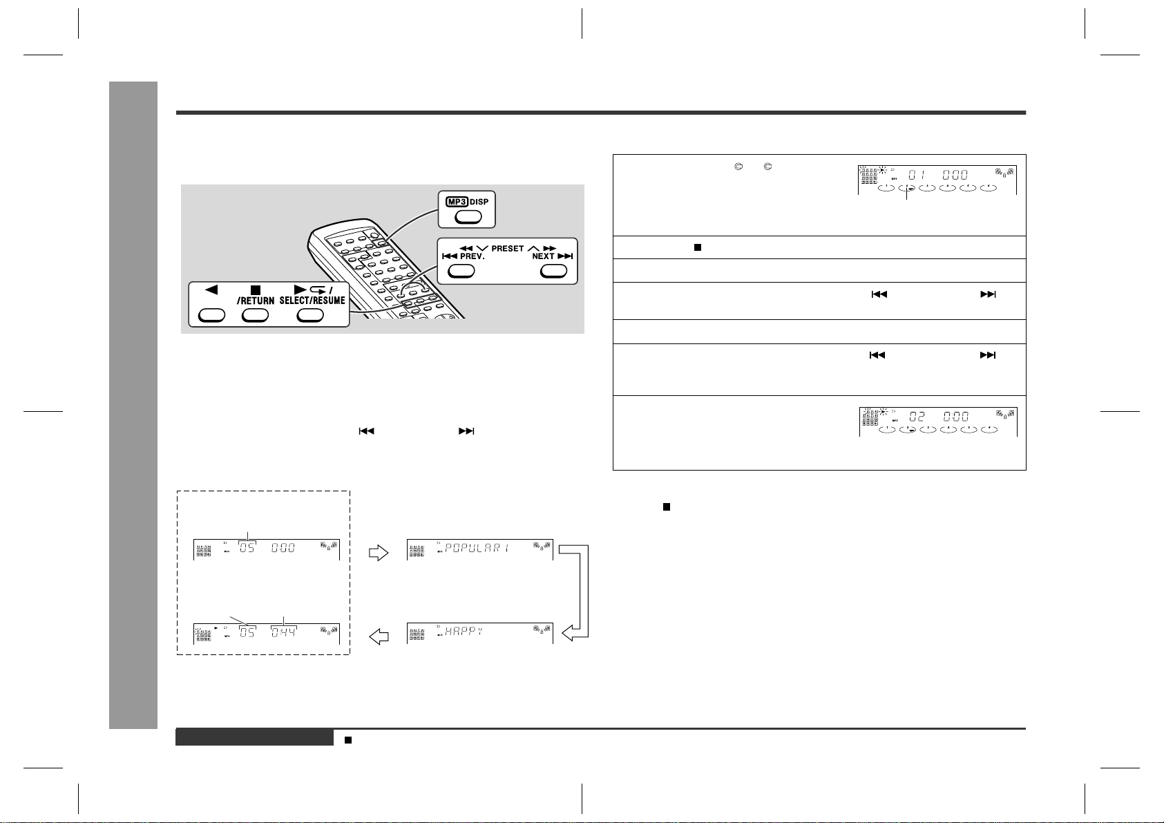
CD-BK3200V
– 30 –
A
B
C
D
E
F
G
H
1
23456
• NOTES ON SCHEMATIC DIAGRAM can be found on page 51.
Figure 30 SCHEMATIC DIAGRAM (3/12)
ACLK
AUDO
AUBCK
AULRCK
+5V
RES
DATAD
LRCK
BLCK
ARCLK
ARFS
AJN
D-GND
TO CD SERVO
P29 11-B
LA14
LA15
LA16
LA17
LA13
LA12
171819
2021222332 31 30 29 28 27 26 25 24
LA9
LA13
LA14
LD6
LA17
LD7
LA8
LA10
LA11
LD5
LD4
LD3
PJM
VCC
A17
A14
A13
A8
A9
A11
OE_
A10
CE_
D7
D6
D5
D4
D3
123456789
10 11 12 16151413
LA3
LA2
LA16
LA15
LA12
LD0
LA7
LA6
LA1
LD2
LD1
LA5
LA4
LA0
GND
D2
D1
D0
A0
A1
A2
A3
A4
A5
A6
A7
A12
A15
A16
VPP
80 79 78 77 76 75 74 73 72 71 70 69 68 67 66 65 64 63 62 61 60 59 58 57 56 55 54 53 52 51
LA2
LA3
LA4
LA5
LA6
LA7
LA8
LA9
LA10
LA11
LA0
LA1
LD2
LD1
LD0
LD7
LD6
LD5
LD4
LD3
LROMCE#
GND
LA11
LA10
LA9
LA8
LA7
LA6
LA5
LA4
LA3
LA2
LA1
LA0
LCS0#
LCS1#
LOE#
LWR#
LD7
LD6
LD5
LD4
LD3
LD2
LD1
LD0
AUX7
AUX5
AUX6
VCC3
100
99
100
99
98
97
96
95
94
93
92
91
90
89
88
87
86
85
84
83
82
81
82
81
123456789
10 11 12 13 14 15 16 19
20 23 26 27
1817
21 22 24 25 28 29 30
DWE#
RAS#
GND
CAS#
TDMFS
TDMDR
TDMCLK
ARFS
ARCLK
AJN
DOE#
ATFG/SEL_PLL1
ATCLK
AOUT/SEL_PLL0
ACLK
LA17
LA16
LA15
LA14
LA13
LA12
VCC
DBUS15
DBUS14
DBUS13
DBUS12
DBUS11
DBUS10
DBUS9
DBUS8
DBUS7
DBUS6
DBUS5
DBUS4
DBUS3
DBUS2
DBUS1
DBUS0
MA8
MA7
MA6
MA5
MA4
MA3
MA2
MA1
MA0
VCC3
50
49
RFSET#
YUV0
GND
AUX4
AUX3
AUX2
AUX1
AUX0
PCLA
PCLA2X
CPUCLK
HSYNC
VSYNC
YUV7
YUV6
YUV5
YUV4
YUV3
YUV2
YUV1
VCC3
GND
29
30
50
49
48
47
46
45
44
43
42
41
40
39
38
37
36
35
34
33
32
31
DBUS14
DBUS13
DBUS1
DA4
DBUS4
DBUS2
DBUS0
DBUS5
DBUS8
DA3
DA5
DA8
DA0
DBUS6
DBUS3
DA7
DA6
DBUS12
DA1
DBUS7
DBUS11
DBUS9
DBUS15
DA2
DBUS10
1
23456789
10 11 12 13 14 15 16 20191817
40 39 38 37 36 35 34 33 32 31 30
29 28 27 26 25 24 23 22 21
DBUS7
DA3
DA4
DA2
DA5
DBUS2
DBUS1
DBUS0
DBUS5
DBUS4
DA6
DBUS10
DA8
DA7
DA0
DBUS3
DBUS8
DBUS9
DBUS15
DBUS14
DBUS6
DA1
DBUS11
DBUS12
DBUS13
CAS2_
OE_
VSS
D15
D14
D13
D12
VSS
D11
D10
D9
D8
CAS_
A8
A7
A6
A5
A4
VSS VCC
A3
A2
A1
A0
RAS_
WE_
VCC
D7
D6
D5
D4
D3
D2
D1
D0
VCC
VIDEO CD PWB-C (2/2)
+B+B
+B
+B
+B
+B
+B
+
B
9
2
3
1
10
4
2
1
3
VIDEO OUT SIGNAL
CM40
0.01
ZD1
4.3A
CM31 0.022
QM3
KRC104 S
RM41
8.2K
RM32 10
RM33 33
CM30
0.1
CM28
0.022
CM36
100/10
CM38
10/16
RM30 33
QM2
KTC3203 Y
CM39
0.1
RM31 33
RM42 33
CM27
10/16
RM47
1K
RM36
330
RM34
10K
QM4
KTA1271 Y
CM37
0.1
CM35
0.022
CM34
10/16
CM32 100/10
CM29
0.022
RM35
100
CM33
0.022
CM26
0.022
RM45
4.7K
C
M
0
.
RM44 33
RM43 33
ICM4
IX0408AW
EEPROM
ICM2
ES3880F
VIDEO CD DECODER
ICM1
1625635T
DRAM
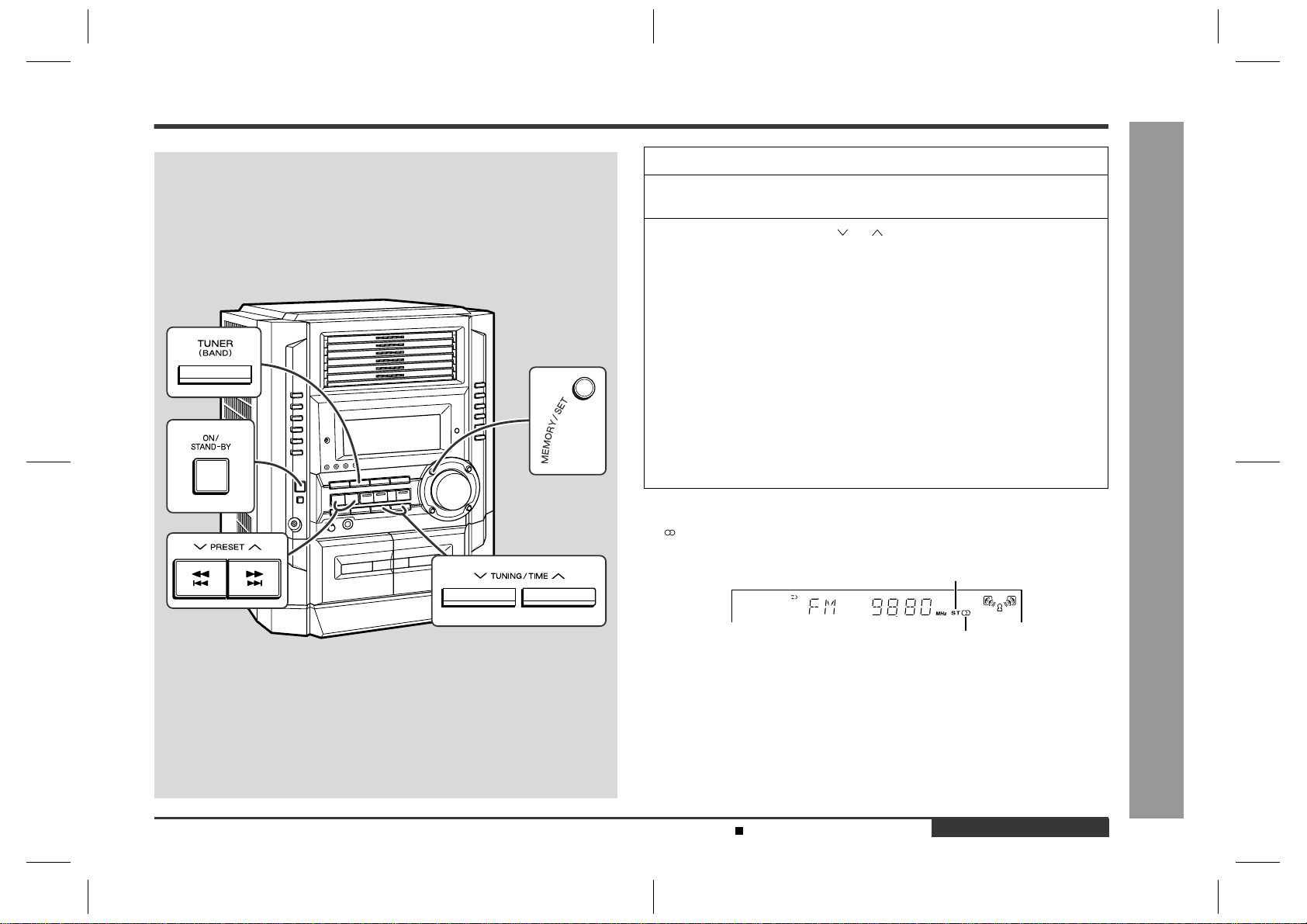
– 31 –
CD-BK3200V
Figure 31 SCHEMATIC DIAGRAM (4/12)
7
8 9 10 11 12
ACLK
AULRCK
AUDO
AUBCK
ARFS
123456789
10 11 12 13 14 15 16 19
20 23 26 27
1817
21 22 24 25 28 29 30
LD1
LD2
LD3
LD4
LD5
LD6
LD7
NC
NC
YUV2
YUV1
YUV0
DSC_D1
DSC_D2
DSC_D3
DSC_D4
YUV3
GND
VDD
YUV4
YUV5
YUV6
YUV7
VSYNC#
DSC_D5
DSC_D6
HSYNC#
DSC_D7
PCK2
PCK
MIC2
AUX14
AUX13
RSCK_SER_IN
AUX12
AUX11
AUX10
RSD/SPLL0
VCC
GND
GND
GND
GND
100
99
98
97
96
95
94
93
92
91
90
89
88
87
86
85
84
83
82
81
81
50
39
38
37
36
35
34
33
32
31
GND
RSTOUT#
RWS/SPLL1
TSCK
TSO
AUX09
TWS/SPLLOUT
AUX08
MCLK
VCC
MUTE
AUX07
RST#
DCLK/EXT-CLK
AUX02
DSC_5
AUX01
DSC_D0
AUX00
DSC_C
VCC
VDD
GND
GND
XIN
VDD
GND
XOUT
AUX03
AUX04
AUX05
AUX06
VDD
PLLCAP
VDAC
VGND
VGND
YDAC
VVDD
VVDD
CDAC
VGND
VGND
COMP
RSET
VCM
VREF
AGND
MIC1
AOL+
AOL–
AOR–
AOR+
AVDD
VREFP
VREFM
AGND
AUX15
49
48
47
46
45
44
43
42
41
40
80 79 78 77 76 75 74 73 72 71 70 69 68 67 66 65 64 63 62 61 60 59 58 57 56 55 54 53 52 51
50
LD0
ARCLK
AJN
7
6
5
3
2
1
8
4
+
–
+
A10V
AGND
R-CH
L-CH
TO CD SECTION
P29 11-C
MPEG POWER
DSA_STB
DSA_DATA
DSA_ACK
HSS_DO
HSS_DI
HSS_STB
HSS_ACK
8
7
6
5
4
3
2
1
2
1
PAL/NTSC
VGND
VDAC
–
+B
+B
+B
+B
+B
+B
+B
+B +B
7
6
5
8
11
TO
CD SECTION
P28 2-E
FROM
DISPLAY PWB
P35 12-B
FROM
MAIN PWB
P33 12-H
CNS705
CNS602
RM83
10K
RM84
10K
CM2
10/16
RM71
3.3K
RM78
4.7K
RM82
10K
RM77
4.7K
QM1
2SC3265 Y
CM1
1000/6.3
RM70
220
RM69
6.8K
RM75
220
RM72
220
RM74
220
CM7
100/16
RM73
2.2K
RM76
56
CM5 100/10
RM81
1K
DM1
1SS133
RM21
22K
CE2
10/16
CNP9
CM43
10/16
CM44
10/16
CM42
10/16
CM41
10/16
CNP10
RM6 33
RM2 33
RM8 33
RM5 33
RM1 33
RM7 33
RM3 33
RM4 33
RM49
4.7K
RM27
4.7K
RM9
150
RM60
10K
CM45
100/10
CM55
22P
RM51
10K
RM65 1K
RM66 1K
RM68
100K
CM53
10/16
CM52
10/16
RM67
100K
CM54
22P
CM50
33P
RM63
22K
RM64
22K
CM51
33P
RM59
10K
RM58 10K
CM49
33P
CM46
33P
RM50
10
RM54
100K
RM55
8.2K
CM48
100/10
CM47
0.1
RM61
10K
RM62
10K
RM53
100K
RM57 100K
RM52
10K
RM56
100K
RM23
4.7K
LM3
3.3µH
XL1
27MHz
RM38
33
RM15
4.7
RM11
150
CM22
10P
CM19
0.1
CM13
0.001
CM14
0.1
CM15
22P
CM17
0.1
CM21
100/10
CM20
0.1
RM16
4.7K
CM18
0.1
RM14
100K
CM12
27P
CM11
27P
CM9
0.1
RM12
150
RM13
150
CM16
0.1
CM8
0.1
RM10
220
CM6
0.1
CM25
0.1
CM24
47/10
CM23
0.1
ICM3
ES3889F
VCD COMPANION
IC6
BA4558F
OPE AMP.
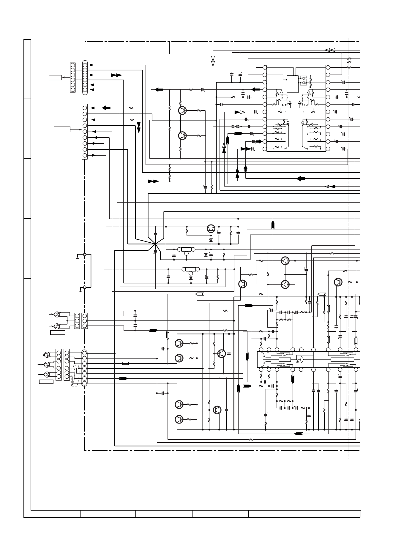
CD-BK3200V
– 32 –
Figure 32 SCHEMATIC DIAGRAM (5/12)
A
B
C
D
E
F
G
H
1
23456
• NOTES ON SCHEMATIC DIAGRAM can be found on page 51.
+5.6V
0V
0V
0.7V
0V
3.4V
3.4V
0V
0V
9.3V
8.6V
9.3V
9V
+B(18V)
0V
0V
0V
0.7V
0.7V
0V
0V
0V
0.7V
0V
0V
0V
0.7V
0V
0V
0V
1
2
3
4
5
6
31
3
1
24
23
22
21
20
19
18
17
16
15
14
13
12
11
10
9
8
7
6
5
4
3
2
1
2
24 23 22 21 20
19
4 1 2 3 5 6 8 9
18 17 16
7
2
M_+12V
A_+5.6V
+10V(A)
GND
9V
+B(+18V)
GND(FAN MOT)
A_+10V
M_GND
GND
M_GND
A_GND
L
M_+12V
A_GND
R-CH
L-CH
CHASSIS
MECHA
BASE
L
R
R
+5.6V(M)
M_GND
L-CH
A_GND
R-CH
T1_R
T1_L
A_GND
M_GND
ERASE
T2_R2
T2_R1
T2_L1
T2_L2
ERASE
HEAD
TAPE 2
RECORD/
PLAYBACK
HEAD
TAPE 1
PLAYBACK
HEAD
R-CH
L-CH
R-CH
L-CH
6
5
1
2
4
3
7
8
9
1
2
3
4
5
6
7
6
1
5
2
4
3
3
4
2
5
1
6
6
3
1
4
3
1
2
5
2
3
1
2
CD
TUNER
DECK
AUX
DI
CE
VSS
LOUT
LBASS
LTRE
LIN
L4
L3
L2
L1
CLK
VDD
VREF
ROUT
RBASS
RTRE
RIN
RSEL0
R4
R3
R2
R1
CCB
INTERFACE
+
–
+
–
+
–
+
–
+
–
+
–
+
–
+
–
LSEL0
–
+
–
+
Hich=T1
+ +
–
–
Hich=CHROME
56K
112K
56K 112K
TO
VIDEO
CD PWB
P29 11-B
FROM
AMP. PWB
P36 1-E
2
3
1
1
3
2
+B
+B
+B
+B
+B
+B
+B
+B
+B
+B
+B
+B
+B
+B
+B
+B
+B
+B
+B
MAIN PWB-A (1/2)
CNP8
CNP906
IC101
IC601
R618
3.9K
R617
3.9K
C606
100/16
C604
0.022
Q604
KTC3199 GR
Q603
KTC3199 GR
R614
680
R613
680
R611
100K
R612
100K
CNP806
BI601
R610 330
R609
330
C629
1/50
C627
1/50
C625
1/50
C623
1/50
C621
10/50
C617
22/50
R619
22K
R615
2.2K
R616
2.2K
C611
0.0027
(ML)
R605
3.9K
C607
0.1(ML)
C609
0.1(ML)
R607
10K
C613
2.2/50
C619
1/50
R64
2
R64
3
R641
C630
1/50
C628
1/50
C626
1/50
C624
1/50
R60
6
3.9
K
C614
2.2/5
0
C608
0.1(ML)
C610
0.1(ML)
C6
0.002
7
C602
22/50
C620
1/50
C62
2
10/5
0
R112 15K
Q110
KRC104 M
R114
10K
Q122
KTC3199 GR
R154
10K
R155 150
Q109
KTA1266 GR
Q111
KRC104 M
C153 100/16
R113
10K
R115
4.7K
R156
220K
R132
33K
C124
0.0022
R124
2.7K
R126
5.6K
C122
47/25
C120
560P
R174
1K
R134 68K
R136 3.9K
C132 270P
C136
0.022
R140 1.5K
C134
22/50
R142
100
C140
0.0033
C142
47/25
R138
6.8K
R120
56
R173
1K
R171
1K
R169
1K
C111
330P
C113
330P
R117
1K
R119
56
C115
47/25
R172
1K
C114
330P
R170
1K
C112
330P
R118
1K
R122
100K
C118
0.033
C116
47/25
C117
0.033
R121
100K
Q106
2SC1845 F
R106
3.3K
R103
2.2K
R105
3.3K
R104
2.2K
Q104
2SC1845 F
Q105
2SC1845 F
Q103
2SC1845 F
R101
1K
Q108
KTC3199 GR
C108 560P
R110 4.7K
C101
560P
R108
47K
C105
180P
C106
180P
R102
1K
C102
560P
R111
15K
R107 47K
C107
560P
R109
4.7K
Q107
KTC3199 GR
R141
100
C127
0.022
C123 0.0022
R131
33K
R135 3.9K
C121
47/25
C119
560P
R125
5.6K
R123
2.7K
C128
3.3/50
R137
6.8K
C139
0.0033
C135 0.022
C133
22/50
C131
270P
C
4
7
R139 1.5K
D801
DS1SS133
D802A
DS1N404S
C861
4700/16
DZ801
DZ2.4BSB
C851
22/50
R852
22K
C855
0.047
(ML)
Q851
KIA7810 AP
Q850
KTC2026 Y
C850
2200/35
C858
0.047
(ML)
R853
22K
C852
0.047(ML)
C860
47/25
Q852
KIA7805 AP
R856
560
C857
47/25
R854
10K
BI102
CNP101
CNS601
IC601
LC75341
AUDIO PROCESSOR
VOLTAGE
REGULATOR
VOLTAGE
REGULATOR
Q109~Q111
SWITCHING
Q103~Q108
SWITCHING
LUG901
CNS102
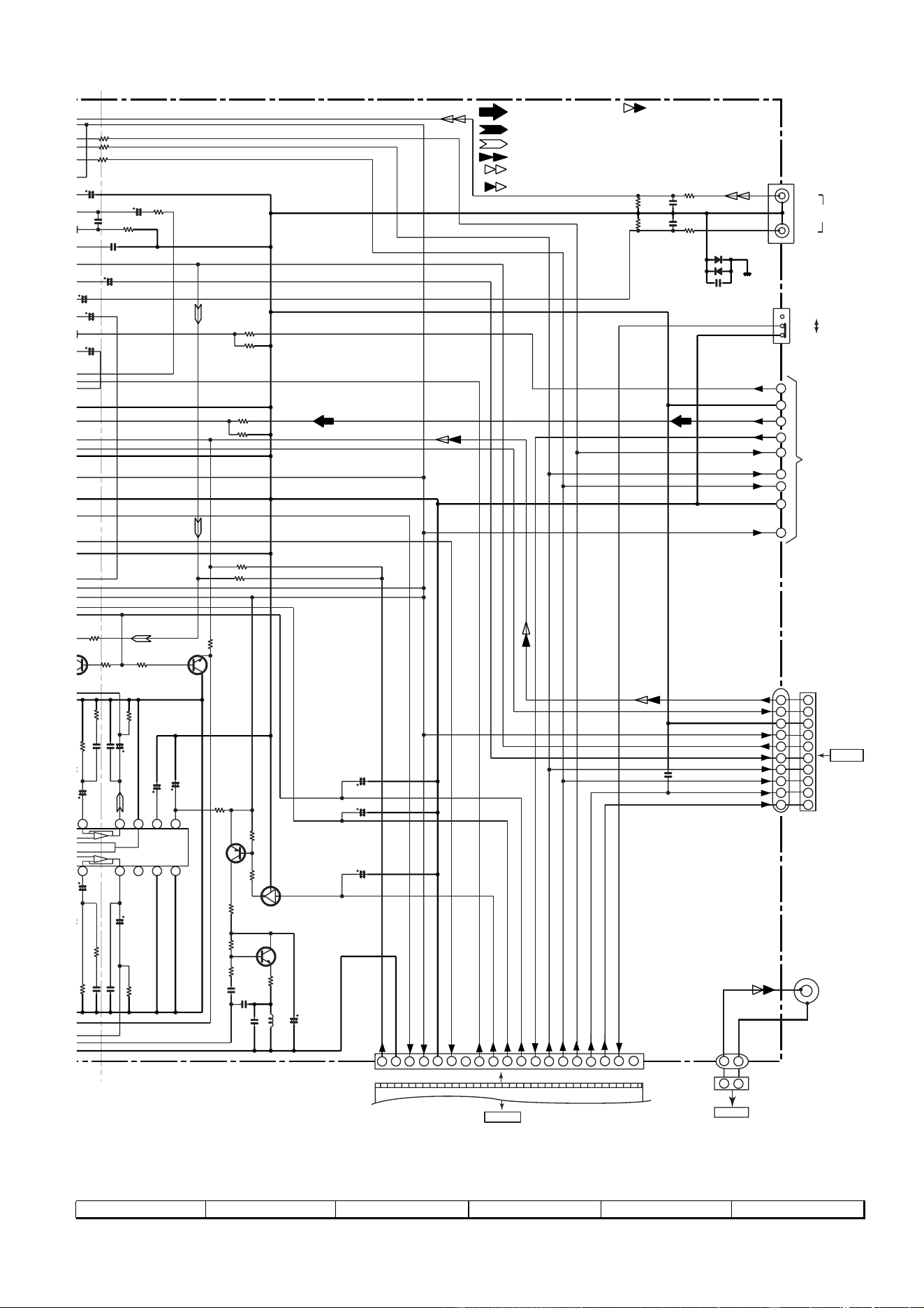
– 33 –
CD-BK3200V
Figure 33 SCHEMATIC DIAGRAM (6/12)
7
8 9 10 11 12
0V
0V
0V
11.6V
0V
0V
0V
11.7V
11.6V
0.7V
0.7V
0V
CD SIGNAL
VIDEO IN SIGNAL
VIDEO OUT SIGNAL
MIC SIGNAL
RECORD SIGNAL
PLAYBACK SIGNAL
FM SIGNAL
1 19
FFC702
1
2
3
4
5
6
7
8
9
CNP702
CNPK1
8 9
10 11
17 16 15 14 13
12
GND A
TUN_L
GND
A_+10V
CE
CLK
DO
DI
TUN_R
REC_L
REC_R
SPAN
KOK_LATCH
S_MUTE
TUN_SM/SPAN
MIC IN
CE
CLK
DI
DO
REC/PLAY
T-T1 T2
T_BIAS
–20dB ATT
+5V
A_+10V
D_GND
M_+12V
M_GND
AIN
KOK IN(R)
KOK OUT(R)
KOK IN(L)
KOK OUT(L)
–20dBATT
KOK LATCH
MIC IN
CLK
DI
KOK IN(R)
KOK OUT(R)
A_+10V
A_GND
KOK IN(L)
KOK OUT(L)
CHASSIS
R
TO TUNER SECTION
P38 1-G
VIDEO IN
R-CH
L-CH
1
2
3
4
5
6
7
8
9
10
1
2
3
4
5
6
7
8
9
10
5
14
3
7
8
9
10
11
12
13
19
18
1714 15 16
Vcc
ALC
GND
ALC
RIPPLE
Nor/CrO2
+
+
–
–
=CHROME
56K
56K
2
6
TO
DISPLAY PWB
P34 1-F
10 kHz/100 kHz
9 kHz/50 kHz
FROM
MIC PWB
P39 12-C
+B
+B
+B
+B
+B
+B
+B
+B
+B
+B
+B
+B
+B
+B
+B
B
+B
+B
+
B
+B
2
1
2
1
CNP10
TO VIDEO CD
PWB
P31 12-C
SWITCHING
BIAS
BIAS OSC
R625 15K
R626
15K
R623 6.8K
R624
6.8K
R642 1K
R643 1K
R641 1K
C
630
1/50
C
628
1/50
C626
1/50
C624
1/50
R606
3.9K
C614
2.2/50
R608
10K
6
08
(ML)
C610
0
.1(ML)
C612
0.0027(ML)
C602
22/50
C
620
1/50
C622
10/50
R638
180K
R637 180K
Q121
KTC3199 GR
R153
10K
Q122
KTC3199 GR
R154
10K
5
0
R156
220K
R157
220K
C136
0.022
C146 220/10
C145 22/50
R140
1
.
5K
C134
22/50
R142
100
C140
0.0033
C142
47/25
R146 10K
R141
100
C139
0.0033
C135 0.022
C133
22/50
C141
47/25
R139
1
.
5K
R145
10K
C157
1/50
C155
22/50
C156
47/25
C154
0.047(ML)
C150
0.0082
(PP)
C151
0.039(ML)
R160
82(1/2W)
Q128
KTC3203 Y
C152
47/25
R164
4.7K
Q124
2SA1015 GR
R162
47K
R158
220
R166
22K
R168
4.7
L104
330µH
Q126
KRC104 M
R167
47K
C654 100P
C634
0.001
SW601
D602
DS1SS133
C631
390P
JK601
VIDEO
/AUX
IN
R631
6.8K
D601
DS1SS133
R634
33K
C632
390P
R633
33K
R632
6.8K
CNP602
BI602
JK671
VIDEO OUT
CNS602
CNSK1
BIK1
SW601
SPAN
SELECTOR
IC101
AN7345K
PLAYBACK AND RECORD/
PLAYBACK AMP.
Q121,Q122
MUTING
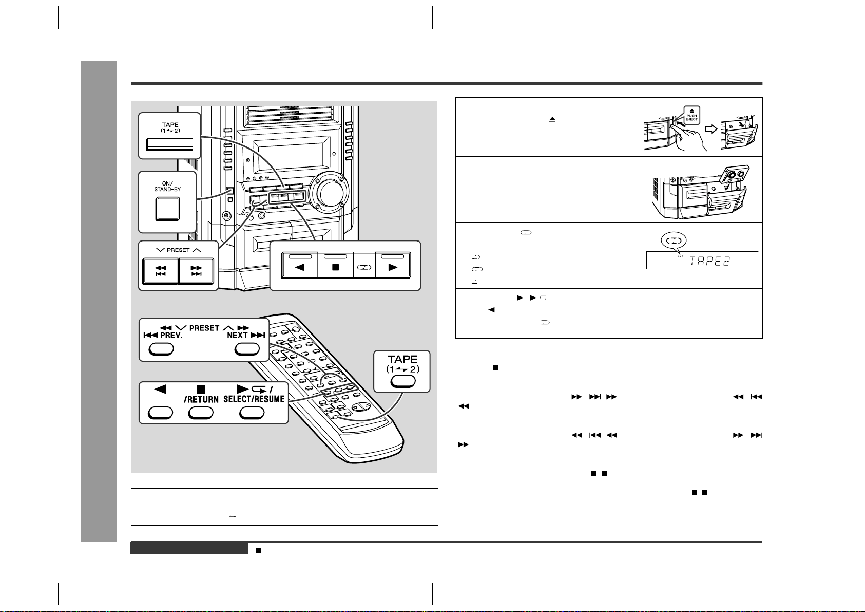
CD-BK3200V
– 34 –
A
B
C
D
E
F
G
H
1
23456
• NOTES ON SCHEMATIC DIAGRAM can be found on page 51.
Figure 34 SCHEMATIC DIAGRAM (7/12)
+B
+B
+B
+B
+B
+B+B
+B
+B
+B
+B
+B
+B
+B
+B
+B +B
+B
+B
65 64 63 61 60 59 58 57 56 55 54 53 52 51 50 49 48 47 46 45 44 43 42 41 40 39 38 37 36 35 34 33 32 31 30 29 28 27 26 25 2
4
1
19
18
17
16
15
14
13
12
11
10
9
8
7
6
5
4
3
2
1
100
99
98
97
96
95
94
93
92
91
90
89
88
87
86
85
84
83
82
82
81
81
50
49
48
32
31
44
43
42
41
40
39
38
37
36
35
34
34
22
22
21
20
19
18
17
16
15
14
13
12
12
23 24 25 26 27 28 29 30 31 32 33
11
10
987654321
80 79 78 77 76 75 7 4737271706968676665646
3
16 17 1
8
213456789
10 11 12 13 14 15
MICIN
KLATCH
CEO
CLK
DI
DO
REC/PLAY
T_T1/T2
T_BIAS
–20DBATT
P13
P12
P11
P10
P1
P2
P3
P4
P6
P8
SPRLY
SP_DET
ANI1
ANI2
ANI3
ANI4
ANI5
P9
P7
P5
MICIN
G4
G5
G6
G9
G10
G11
G12
G13
G14
G15
G16
P22
P23
P24
P25
P26
P27
P28
P29
P30
P31
P32
P33
P34
P35
P36
P37
P38
P39
P40
P41
P41
P40
P39
P38
P37
P36
P35
P34
P33
P32
P31
P30
P29
P28
P27
P26
P25
P24
P23
P22
G16
G15
G14
G13
G12
G11
G10
G9
P1
P2
P3
P4
P5
P6
P7
P8
P9
P10
P14
P15
P16
P17
P18
P19
P20
P21
G1
G2
G3
G7
G8
KLATCH
BACK_UP
SO
+VF2
VF1
–VF
P_IN
UN_SW 5V
/SPEANA SEL C
/SPEANA SEL B
M_GND
KEY2
KEY1
RES
VPP
SI
D-GND
VDD
BG1
BG2
BG3
BG4
BG5
BG6
BG7
BG8
BS1
BS2
BS3
BS4
BS5
BS6
BS7
BS8
BS9
BS10
BS11
BS12
BS13
BS14
BS15
BS16
BS17
BS18
BS19
BS20
DISPLAY PWB-B1
AIN
SPN/TUN_SM
GND
AOUT
TEST
SEL
C
B
A
VCC
AIN
CIN
DIFOUT
RREF
VREFC
BIASC
STB
CLK
DIN
DOUT
OSC
VEE
VDD
VDD
VSS VSS
D_GND
A_+10V
+5V
M_+12V
100
FIP0
FIP1
FIP2
FIP3
FIP4
FIP5
FIP6
FIP7
FIP8
FIP9
FIP10
FIP11
FIP12
FIP13
FIP14
FIP15
FIP16
FIP17
FIP18/SPEANA SEL A
FIP19
VLOAD
VDD2
FIP20
FIP21
FIP22
FIP23
FIP24
FIP25
FIP26
FIP27
FIP28
DIST IN
MPEG_POW
KARAOKE LATCH
FL LATCH
MIC SW
JOG 1
JOG 0
DSA_STB
DSA_DATA
AC3_SCK/D
S
TIMER LE
D
DO
VDD1
X2
X1
VSS1
AVSS
TUN_SM/SPN
T2RUN
T1RUN
KEY2
KEY1
KEY0
ANI5
ANI4
ANI3
ANI2
ANI1
AVDD
SPEANA
A OUT
9
8
7
6
5
4
3
2
1
9
8
7
6
5
4
3
2
1
6
54321
16
19
2
1
3
4
5
6
7
8
9
10
11
12
13
14
15
17
18
TO MAIN PWB
P33 10-H
TO POWER PWB
P36 1-F
CNP905
CNP602
RS701
1K
RS702
1K
C727
0.0015
R703
82K
R702
47K
R701
47K
C702
47/25
C701
0.022
IC702
D16315GB
FL DISPLAY
DRIVER
FL701
FL DISPLAY
C703
47/50
C705 47/25
R708
1K
R709 1K
R710 1K
R707 33
R704
100K
R705
100K
R706
100K
Q703
KTC3199 GR
Q702
KTC3199 GR
Q701
KTC3199 GR
R761 10K
R762 10K
R766 10K
R792 10K
R798 10K
C706
0.022
R727 1K
C714
220/10
C713
0.022
R717 10K
R716 10K
XL701
C712
15P
C711 18P
R719 1K
R724 1K
R725 1K
R726 1K
R728 1K
R729 1K
R723 1K
R722 1K
R721 1K
R720 1K
R712
47K
R713
10K
R714
10K
R715
10K
D711
DS1SS133
D713
DS1SS133
D712
DS1SS133
C709
0.1
C708 0.1
C707
0.1
C710
0.1
IC703
BA3835F
5 BAND PASS
FILTER
R711
100K
CNP702
D717
DS 1SS133
D716
DS1SS133
BI701
IC701
IX0413AW
SYSTEM MICROCO
M
D708
DS1SS133
R775 1K
R745
10K
D701
DS1SS133
D703
DS1SS133
D705
DS1SS133
R776
10K
C704
0.022
R777
10K
R770 100
R771 100
R772 1K
R773 1K
R774 1K
R718 1K
CNS905
FFC702
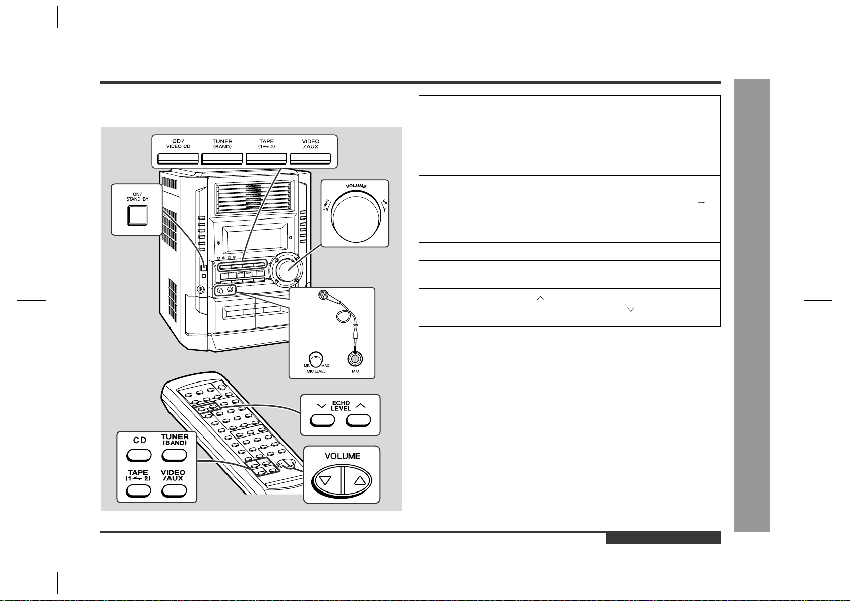
– 35 –
CD-BK3200V
7
8 9 10 11 12
Figure 35 SCHEMATIC DIAGRAM (8/12)
+10V
+B
+B
+B
+B
+B
+B
+B
+B
+B
+B
+B
+B
29 28 27 26 25 24 23 22 21 20
19 18 17 16 15 14 13 12 11 10
98765 321
2
1
3
M
9
10
8
7
6
5
4
3
2
1
1
10
10
1
+
-
TAPE MECHANISM PWB-H
TAPE
MOTOR
PLAY
F. PLAY
CASSETTE
SOLENOID
SOLENOID
PH
FFC701
FFC701
EJECT
SWITCH
PWB-B2
18
17
16
15
14
13
12
11
10
9
8
7
6
5
4
3
2
1
50
49
5
0
4
9
48
4
8
47
46
45
44
43
42
41
40
39
38
37
36
35
34
33
32
32
31
31
67 66 65 64 61 60 59 58 57 56 55 54 53 52 5163 62
16 17 18 19 20 21 22 23 24 25 26 27 28 29 3014 15
123
PIN8
PIN7
PIN5
PIN3
PIN4
PIN1
PIN2
PIN6
PIN8
PIN5
PIN4
PIN3
PIN2
PIN1
PIN7
PIN6
P65
DISC6
DISC5
DISC4
DISC3
DISC2
DISC1
P25
P26
P27
P25
P26
P65
P27
P66
P67
P47
ANI4
ANI5
ANI1
ANI3
ANI2
DISC6
DISC5
DISC4
DISC3
DISC2
DISC1
P47
DI
CLK
DO
CEO
SP_DET
MICIN
P5
P6
P7
P8
P9
P10
P11
P12
P13
P14
P15
P16
P17
P18
P19
P20
P21
G1
G2
G3
G4
G5
G6
G7
G8
P67
P66
T_BIAS
T_T1/T2
REC/PLAY
SPRLY
KLATCH
–20DBATT
MPEG_POWER
DSA_STB
DSA_DATA
DSA_ACK
ESS_DO
ESS_DI
ESS_STB
ESS_ACK
SO
SCK
GND
KEY0
PLAY
STOP
RES
VPP
SI
VDD
FPA
GND
T1RUN
FPB
SOL_A
SOL_B
T_MOTOR
T2RUN
PLAY_SW_B
Q10
VDD
OE
Q11
Q9
Q8
Q7
Q6
Q5
Q4
Q3
Q2
Q1
Q0
LCK0
CLOCK
DATA
VSS
KEY0
KEY1
KEY2
CAM_A SW_A/CAM_A SW_B
CAM_A SW_C/CAM_A SW_D
CAM_A SW_E/CAM_B SW_A
CAM_B SW_B/TRAY SW_A
TRAY SW_B/TRAY SW_C
CD DO
CD DI
CD CLK
CD CE
WRQ
DRF
RESOUT
KARAOKE LATCH
FL LATCH
MIC SW
JOG 1
JOG 0
SP DET
SMUTE
–20dBATT
LCK 1
LCK 0
AC RLY
H ONLY
SPRLY
CE_2
CE_1
T_BIAS
T_T1/T2
REC/PLAY
DSA_STB
DSA_DATA
AC3_SCK/DSA_ACK
AC3_SO/RDS READY/ESS_DO
AC3_SI/RDS RDCL/ESS_DI
AC3_SS_/RDS RDDA/ESS_STB
AC3_RST/RDS RST/ESS_ACK
RESOUT
RESET
VDD0
VSS0
FPB
FPA
PLAY SW B
PLAY SW A
T_MOTOR
T_SOL_B
T_SOL_A
TIMER LED
DO
DI
CLK
CE_0
P_IN
DRF/DVD BUS 5
WRQ/DVD BUS 4
CD CE/DVD BUS 3
CD CLK/DVD BUS 2/SCK
CD DI/DVD BUS 1/SI
CD DO/DVD BUS 0/SO
REMOCON
IC(VPP)
VDD1
X2
X1
VSS1
AVSS
1
3
8
5
6
7
4
2
1
3
8
5
6
7
4
2
2
1
2
11
2
765432
10
9
8
7
6
5
4
3
2
1
9
8
7
12
10
2
1
11
6
5
4
33
4
5
6
11
12
7
8
1
2
9
10
1
2
3
4
5
6
8
9
7
1
2
3
4
5
6
8
9
7
TO
VIDEO CD PWB
P29 11-D
TO VIDEO CD PWB
P31 12-B
SOLENOID DRIVER
SOLENOID DRIVER
MOTOR DRIVER
CNP9
CNP7
PLAY SWITCH PWB-B3
R769 1K
D714
DS1SS133
C
714
20/10
C713
0.022
R737 1K
R738 1K
R739 1K
R740
1K
XL701
4.194304 MHz
C712
15P
C711 18P
R735 1K
R734 1K
R733 1K
R731 1K
R730 1K
R732 100
R779 10K
R780 10K
R781 10K
RD35
33K
RD34
15K
SW737
REC
PAUSE
SW738
X-BASS/
DEMO
SW736
TUNING
DOWN
RD25
680
RD30
2.7K
RD29
2.2K
RD32
5.6K
RD26
820
RD28
1.5K
RD27
1K
RD31
3.9K
RD33
10K
SW735
TUNING
UP
SW729
REVERES
PLAY
SW730
STOP
SW728
FAST
FORWARD
SW733
CLOCK
SW734
TIMER/
SLEEP
SW731
REVERSE
MODE
SW732
PLAY
SW727
FAST
REWIND
D715
DS1SS133
C725
47/25
C724
0.022
RX701
REMOTE
SENSOR
R785
100
C723
0.022
D718
DS1SS133
R784
100K
R783
47K
R782 10K
Q707
KRC102 M
RESET
C722
3.3/50
LED714
LED714~LED718
SLR325MC
LED716
LED718
LED717
LED715
LED725 SLR325MC
RD06
2.7K
RD09
10K
RD10
15K
SW706
DISC 1
PLAY
SW707
DISC 2
PLAY
SW708
DISC 3
PLAY
SW709
DISC 4
PLAY
SW710
DISC 5
PLAY
SW711
DISC 6
PLAY
RD08
5.6K
RD07
3.9K
RD11
33K
RD12
100K
RD22
15K
SW721
DISC 1
EJECT
RD20
5.6K
RD21
10K
SW704
O.S.D.
SW703
P.B.C.
SW702
KARAOKE
BI703A
CNP704
RD04
1.5K
RD03
1K
RD05
2.2K
RD02
820
RD01
680
BI703B
BI702
CNS702
SW701
ON/
STAND-BY
RD14
820
RD17
2.2K
RD15
1K
SW720
EQUALIZER
SW719
MEMORY
SET
SW717
TUNER
(BAND)
RD19
3.9K
SW715
CD
SW716
TAPE
SW718
VIDEO/
AUX
RD16
1.5K
SW714
DIMMER
RD13
680
RD18
2.7K
CNP703
C
701
413AW
C
ROCOMPUTER
R754 1K
R753 1K
R752 1K
R751 1K
R749
1K
C728
470P
C721
0.022
RS725
68K
RS706
1.5K
RS709
1.5K
RS710
1.5K
LED711
4204UYT1
LED710
4204UYT1
LED709
4204UYT1
RS724 560
RS716 560
RS715 560
RS713 560
RS717 560
RS714 560
R788
10K
R791 10K
R790 10K
R789 10K
R746 1K
R797
10K
R795
10K
LED701
4204SRT1
C715
0.022
R750 1K
R741 1K
R742 1.8K
R743 2.2K
Q705
KTA1273 Y
Q706
KTA1273 Y
Q704
KTA1273 Y
R744 2.2K
R799 2.2K
R747 1K
R748 1K
R787
10K
R786
10K
IC705
BU2092F
INPUT/OUTPUT EXPANDER
BI705
BI704
CNP701
RS703 10K
5
R736 1K
7
6
K
R777
10K
R793
10K
R794
10K
R770 100
C726
47/50
R760
47K
R763 1K
R765 1K
R767
1K
R771 100
JOG701
JOG
VOLUME
C716
0.001
C717
0.001
R758
1K
R759 1K
R772 1K
R773 1K
R774
1K
CNS705
CNS704
SW705
DIGEST
SW722
DISC 2
EJECT
SW723
DISC 3
EJECT
SW724
DISC 4
EJECT
SW712
DISC 5
EJECT
SW713
DISC 6
EJECT
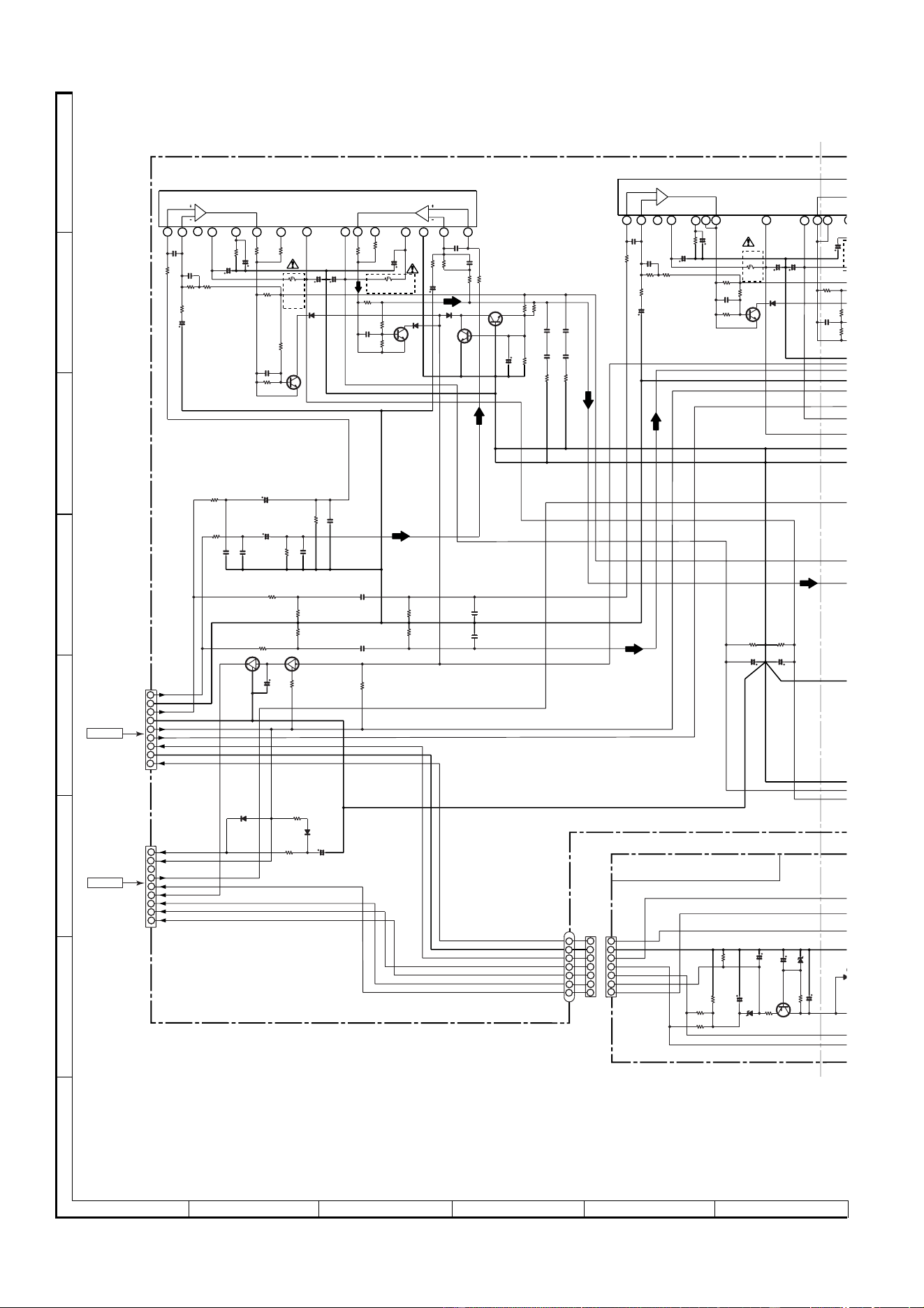
CD-BK3200V
– 36 –
A
B
C
D
E
F
G
H
1
23456
• NOTES ON SCHEMATIC DIAGRAM can be found on page 51.
Figure 36 SCHEMATIC DIAGRAM (9/12)
CNS905
CNS806
+5V(BACK_UP)
SP RLY
SP DET
+5V(UN_SW)
–VF
VF1
VF2
P_IN
9
1
2
3
4
5
6
7
8
GND
+B(+9V)
+B(+18V)
GND
+5.6V
L-CH
A_GND
R-CH
M_12V
9
8
7
6
5
4
3
2
1
–Vcc
+Vcc
Front_L
Ch2
Front_R
Ch1
Ch1
Out
Out
Ch2
15141312
11
10
9 8
7
6
5 4
3
2
1
–Vcc
+Vcc
Ch 2
Out
Out
Ch 1
Ch1
1
1110
9
8 7
6
5
4
3
2
1
L OUT
R OUT
P_IN(SYS REST)
+B(+18V)
+B(+9V)
GND
VF2
VF1
–VF
P_IN(SYS REST)
+B(+18V)
+B(+9V)
GND
VF1
VF2
–VF
4
6
5
4
3
2
1
6
5
4
3
2
1
1
2
3
5
6
7
7
7
L
R
POWER A PWB-D2
1
1
2
2
3
3
FROM
MAIN PWB
P32 1-B
FROM
DISPLAY PWB
P34 1-G
+B
+B
+B
+B
+B
+B
+B
+B
+B
+B
+B
+B
+B +B
R971
68K
C961
0.1(ML)
R997
27K
R998
27K
R970
68K
C960
0.1(ML)
C955
0.082
(ML)
C954
0.082
(ML)
R957
18K
C959
0.22/50
C958
0.22/50
C811
47/50
R806
10K
R808
150
R809
2.2K
D820
DS1SS133
D819
DS1SS133
CNP906
CNP901
BI901
R829
47
R830
47
C809
220/50
R801
2.2K
Q801
KTA1274 Y
ZD801
DZ30BSC
C810
47/50
R802
10
ZD802
DZ6.2BSA
C812
100/35
R804
47K
R803
12K
D81
8
DS1N4
0
CNP905
IC901
STK40270N
POWER AMP.
C991
0.22/50
C990
0.22/50
C917
0.1
(ML)
C916
0.1
(ML)
Q991
KRA107 M
R828
100
C825
3.3/50
Q990
KRC107 M
R805
22K
R819
22K
C814
2200/63
C813
2200/63
R996
0.22
(2W)
R910
100(1/4)Fusible
C904
100/50
R994
0.22
(2W)
R993
0.22
(2W)
R995
0.22(2W)
C943
0.001
C944
0.001
C942
0.015(ML)
C941
0.015(ML)
R974
68K
R975
68K
R973
68K
R972
68K
D905
DS1SS133
R924
100
(1/4)
Fusible
C922
100/50
R956
18K
C923
100/50
R
1
R935
10K
C925
0.022
R933
0.1(1W)
C921
10/50
C920
10/50
Q906
KTC3199 GR
R938
1K
R936
10K
C924
0.022
R934
0.1(1W)
R932
1K
R928
56K
C928
15P
C930
1/50
R930
820
C926
0.0015
R976
1K
R926
22K
C909
15P
R909
1K
R903
56K
R907 560
C911
10/50
D903
DS1SS133
R917
1K
D901
DS1SS133
Q904
KTC3199 GR
C914
47/50
R920
56K
R919
56K
R921
56K
R922
4.7
R923
4.7
C918
0.1
(ML)
C919
0.1
(ML)
Q901
KTC3199 GR
R913
1K
R915
6.8K
C905
0.022
R911
0.1(1W)
D902
DS1SS133
C902
10/50
C901
10/50
Q902
KTC3199 GR
R914
1K
R916
6.8K
C912
0.022
R912
0.1(1W)
R901
100
(1/4)
Fusible
R908
1K
R904
56K
C910
15P
C908
10/50
R906
560
C906
0.0015
R918
1K
C903
100/50
C907
0.0015
Q903
KTC3199 GR
R902
22K
–
+
CNS901
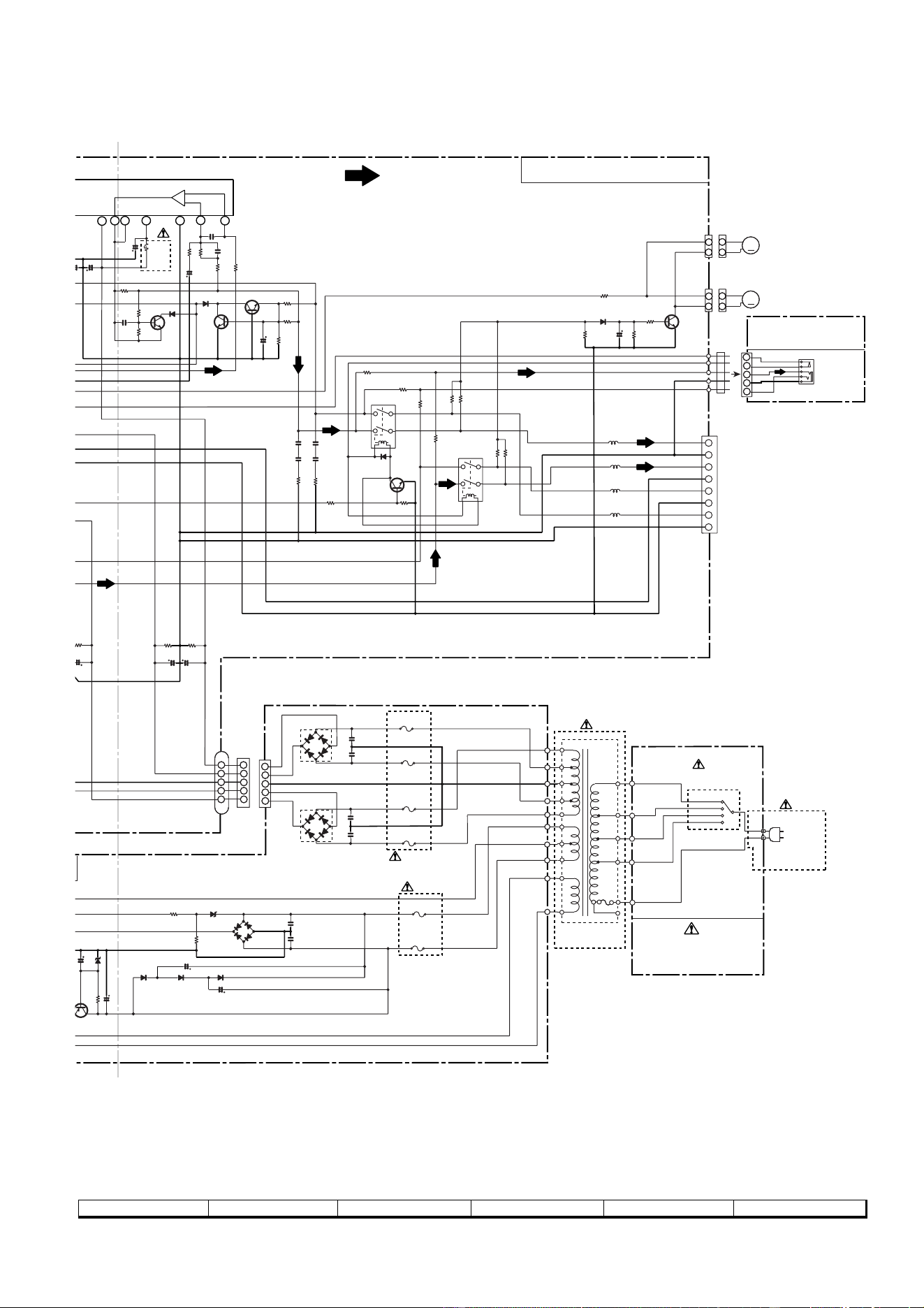
– 37 –
CD-BK3200V
7
8 9 10 11 12
Figure 37 SCHEMATIC DIAGRAM (10/12)
230-240 V
220 V
127 V
110 V
FM SIGNAL
HEADPHONES
PWB-B4
–Vcc
Ch 2
Out
Ch2
151413
12
1110
9
+B
T.F.
1
2
3
4
5
1
2
3
4
5
1
2
3
4
5
SP_R-CH_GND (LOW)
SP_R-CH (LOW)
SP_L-CH_GND (LOW)
SP_L-CH (LOW)
SP_L-CH_GND (HI)
SP_R-CH (HI)
SP_R-CH_GND (HI)
SP_L-CH (HI)
4
2
3
1
5
2
1
2
1
2
1
2
1
+
–
+
–
+
–
+
–
M
M
POWER AMP PWB-D1
POWER B
PWB-D3
AC POWER
SUPPLY CORD
AC 110/127/220/
230-240 V,50/60 Hz
L
R
+
+
–
–
+B
+B
FAN MOTOR
DRIVER
SP RELAY
ON–OFF
R966
22K
R967
22K
SW801
VOLTAGE
SELECTOR
CNP907
IC902
STK40270N
POWER AMP.
R955
4.7(1/2W)
L904
L905
RY902
BI902
C803
0.047(ML)
C804
0.047(ML)
D803
TS6B04GM
F803
T5A L 250V
F802
T5A L 250V
C832
0.047(ML)
C833
0.047(ML)
D802
TS6B04GM
CNP902
F800
T4A L 250V
F801
T4A L 250V
F805
T2A L 250V
D809
DS1N404S
D808
DS1N404S
C808
100/50
C809
220/50
R801
2.2K
Q801
T
A1274 Y
ZD801
DZ30BSC
47/50
C807
100/50
D818
DS1N404S
F804
T2A L 250V
D804
DS1N404S
D806
DS1NS404S
C806
0.047(ML)
D807
DS1N404S
D805
DS1N404S
C805
0.047(ML)
R826
220K
R827
47K
ZD806
DZ11BSB
R944
270(1/2W)
FW901
C939
0.1(ML)
C940
0.1(ML)
R
805
2
2K
C801
2200/50
C802
2200/50
C
813
0
0/63
R979
1K
CNP904
R945
270(1/2W)
L902
L903
D909
DS1SS133
Q910
KTC3203 Y
R952
15K
C938
10/50
R953
68K
R954
1K
SO901
SPEAKER
TERMINAL
Q909
KTC3199 GR
R980
10K
R951
2.2K
R950
2.2K
R949
2.2K
R948
2.2K
RY901
D907
DS1SS133
R946
270
(1/2W)
R947
270
(1/2W)
R942
4.7
C936
0.1(ML)
C935
0.1(ML)
R943
4.7
DS1SS133
R940
56K
R941
56K
R939
56K
Q907
KTC3199 GR
C929
15P
R931
1K
R927
56K
R929
820
C931
1/50
D906
DS1SS133
R977
1K
D904
DS1SS133
Q908
KTC3199 GR
C932
47/50
C923
100/50
Q905
KTC3199 GR
R925
100
(1/4)
Fusible
R937
1K
R935
10K
C925
0.022
R933
0.1(1W)
C921
10/50
2
0
5
0
C927
0.0015
CNS907
T801
POWER
TRANSFORMER
CNS904
–
+
CNS902
JK670
HEADPHONES
M901
FAN MOTOR
M902
FAN MOTOR
K801
K802
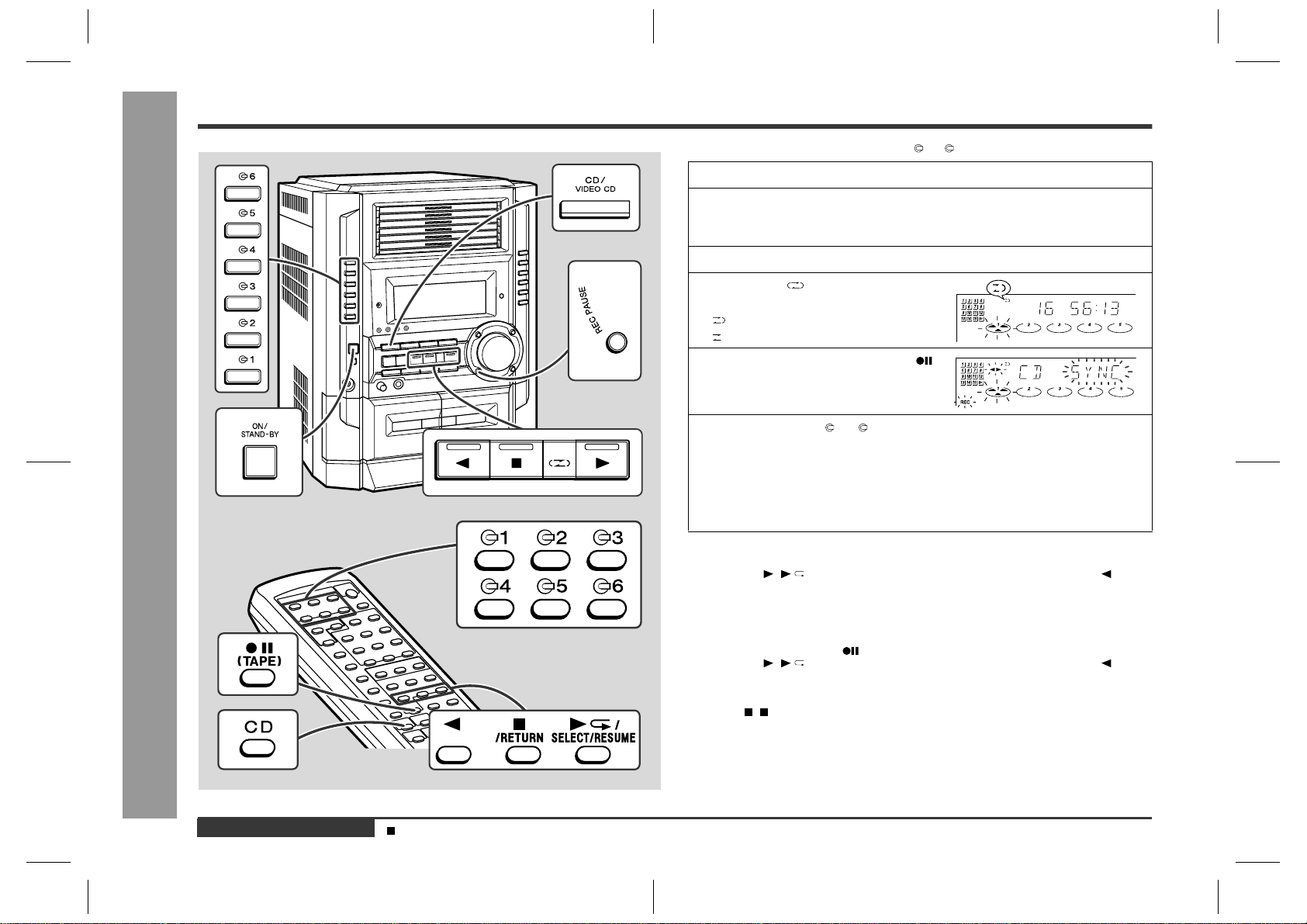
CD-BK3200V
– 38 –
Figure 38 SCHEMATIC DIAGRAM (11/12)
A
B
C
D
E
F
G
H
1
23456
• NOTES ON SCHEMATIC DIAGRAM can be found on page 51.
TP301
IC302
D_GND
CLK
DO
CE
DI
TUN_R
A_GND
A_10 V
TUN_L
AM ANT.
IC303
2
1
1
3
2
3
FM SIGNAL
AM SIGNAL
MAIN PWB-A (2/2)
CHASSIS
GND
CHASSIS
GND
CONSTANT
VOLTAGE
C372
1/50
R356
1K
C374 0.015
R357
470K
C368
1/50
X351
456 kHz
C369
27P(UJ)
C367
1/50
R350
2.7K
C366 0.001
C363 0.022
C364 2.2/50
C365 0.022
C362 3.3/50
C361 0.022
R365
10K
R358
3.9K
C342
0.022
R351 5.6K
R336 10K
R323
68K
C334
22P(CH)
C335
560P
C323
0.022
C331
0.047
C332
0.022
VD301
KDV147B
C373
0.015
C371
1/50
ZD351
DZ5.1BSB
C396
100/10
C395 0.022
R392 270
R391
270
Q360
KTA1266 GR
R383
5.6K
R385
5.6K
C391
47/25
R384
5.6K
R359
1.8K
C388
0.001
R386
22K
R376
1K
R395
47K
R360
4.7K
C386
330P
R377
47K
L351
100µH
C385
0.01
C387
0.022
C380
10/50
C392
0.001
R379
2.2K
R380
1.5K
C393
1/50
C394
47/25
R381
10K
R393
1K
CF351
C354 0.022
C353 0.022
CF352
T351
AM IF
R352
1K
C356
0.001
C357
2.2/50
R355
3.3K
C370
1/50
R388
3.9K
C398
100/10
C399
0.022
R387
5.6K
L352
100µH
C358
1/50
C352 10/50
C350 0.022
C351 0.022
C397
0.022
R382
150
C381
12P(CH)
X352
4.5 MHz
C382
15P(CH)
R375
470
C384
0.001
R378 1K
R372 1K
R374 1K
R373 1K
R316
4.7K
CF303
C318
100P
C313
22P(CH)
R309
10K
C324
3.9P(UJ)
VD303
SVC211C
C312
0.022
C306
0.022
C307
10/50
C311
18P
R302
10
IC301
TA7358AP
FM FRONT END
C305
4.7P
(CH)
C310 15P(CH)
BF301
B.P.F.
C303
10P(CH)
C304
0.01
CNP301
SO302
FM ANTENNA
TERMINAL
L312
D305 DS1SS133
C308
4.7P(UJ)
R311
100K
C309
0.001
VD302
SKDV147B
R313
33K
R314
22
C317
0.001
C316
0.022
C315
0.0047
C314
0.0047
R327
33
R325
47K
R322
680
Q302
KTC3194 Y
OSC BUFF
R353
270
C355
22P
T303
AM TRACKING fL
AM BAND
COVERAGE fL
T306
AM OSC.
FM RF
T301
FM OSC.
T302
FM IF
IC302
LC72131
PLL(TUNER)
IC303
LA1832S
FM IF DET./FM MPX./AM IF
C330
15P
D302
DS1SS133
D301
DS1SS133
C338
0.001
C320
0.001
CONT
IF
FM/AM
FM/AM
AM LOOP
ANTENNA
SD
MO/ST
ST IND
MO/ST
VSS
AOUT
AIN
PD
VDD
FM IN
AM IN
DO
CL
DI
CE
X IN
X OUT
IF IN
REG
AM IF IN
GND
SD
STEREO
FM DET
VCC
IF OUT
PHASE
(FM/AM)
PHASE
L-CH OUT
R-CH OUT
MPX IN
MPX VCO
FM/AM OUT
VSM
AM LOW CUT
AM RF IN
AM OSC IN
FM AFC
AM OSC OUT
AM MIX OUT
FM IF IN
9
8
7
6
5
4
3
2
1
24
23
22
21
20
19
18
17
16
15
14
13
12
11
10
1
1
2
3
4
5
6
7
8
9
2
3
4
5
6
7
8
9
3
2
2
2
1
1
1
TP302
22
21
20
19
18
17
16
15
14
13
12
11
10
TO MAIN SECTION
P33 12-C
1
2
3
4
5
6
7
8
9
+B
+B
+B
+B
+B
+B
+B
+B
+B
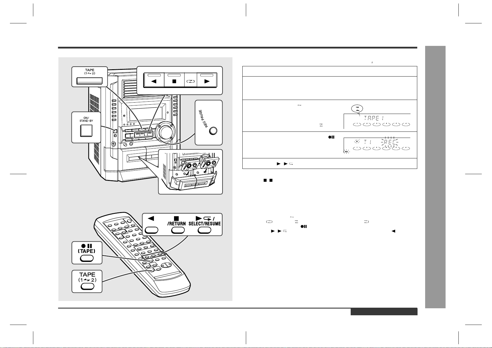
– 39 –
CD-BK3200V
Figure 39 SCHEMATIC DIAGRAM (12/12)
1
2
3
4
5
6
7
8
9
10
MICSW
DATA
CLOCK
LATCH
PS2
PS1
VCF IL
L OUT
R OUT
SOURCEOUT
KEYCONIN
R IN
L IN
VOL IN
LPF2OUT
LPF2IN2
LPF2IN1
DAINTOUT
DAINTIN
DACONT
VCC
GND
MCLKCONT
VACL
MIC1 IN
ALC1
ALC2
MIC1NF IN
MIC2NF IN
MIC1 OUT
MIC2 OUT
MIC1VOL IN
MIC2VOL IN
MICOUT
LPF1 IN1
LPF2 IN2
LPF1 OUT
AD INTIN
ADCONT
REF
AD INTOUT
MIC2 IN
MIC SIGNAL
42
41
40
39
38
37
36
35
34
33
32
31
30
29
28
27
26
25
24
23
22
12
11
10
9
8
7
6
5
4
3
2
1
21
20
19
18
17
16
15
14
13
8
7
6
5
4
3
2
1
MIC IN
DI
CLK
KOK LATCH
KOK IN(R)
KOK OUT(R)
A_+10V
A_GND
KOK IN(L)
KOK OUT(L)
CHASSIS
GND
ICK2
KIA4558P
MIC PWB-J
TO
MAIN PWB
P33 12-E
CNSK1
+B
+B
+B
RK40
1k
RK37
390
RK39
1k
CK41
100/16
CK10 0.1
CK11 0.1
CK7 0.47/50
CK44
47/25
CK72
100/16
RK42 10K
VRK1
20K(B)
MIC
VOLUME
CK53
47/25
RK48
10K
RK50
10K
CK47
220P
RK43
18K
CK48 220P
RK46
18K
CK45
2.2/50
CK46
2.2/50
RK49
10K
RK41 10K
CK51
1/50
CK52
1/50
RK47
8.2K
RK45
6.8K
RK44
6.8K
CK49
100P
CK50
100P
CK42
0.022
RK38
100
RK14
100
RK15
100
RK36
390
CK19
0.022
RK8 5.6K
CK23 0.001
CK1 0.01
RK11 1K
RK10 1K
RK9 1K
CK43
47/25
ZDK1
MTZJ5.6B
RK12
100
RK13
1.2K
QK1
KTC3203 Y
ICK1
M65856SP
MIC AMP.
RK2 56K
RK3
56K
RK4 10K
RK7
1K
JK1
MIC
CK9 2.2/50
CK8 4.7/50
CK13
0.0047
CK17
220/10
CK18
100/16
CK16 0.22
CK15 0.068
CK25 2.2/50
CK26 2.2/50
CK12
2.2/50
CK14 0.001
CK21 0.068
CK24 2.2/50
CK33 47P
CK30 2.2/50
CK29 2.2/50
CK31 0.15
CK35 47P
CK34 47P
CK22 0.0047
CK20 0.22
DK1
DS1SS133
PINK1
DK2
DS1SS133
RK1
10K
IC903
KIA4558P
OPE AMP.
CNPK1
Figure 39 WIRING SIDE OF P.W.BOARD (1/11)
7
8 9 10 11 12
MIC PWB-J
PINK1
CNSK1
FROM
MAIN PWB
P41 8-A
JK1
MIC
VRK1
MIC VOLUME
5
6
7
8
4
3
2
1
RK48
CK44
CK72
RK47
RK42
ZDK1
RK43
RK41
RK13
RK38
CK47
RK12
CK43
RK44
QK1
CK52
CK42
CK49
CK45
RK49
RK14
RK15
RK36
CNPK1
10
9
8
7
6
5
4
3
2
1
RK39
CK7
RK40
RK4
RK1
CK1
CK31
CK41
CK33
CK34
RK2
RK3
CK35
CK30
RK11
RK10
CK29
1
5
10
15
20
22
25 30 35 40
42
21
CK26
CK25
CK24
RK9
RK37
CK18
CK23
CK22
CK21
CK20
CK19
CK13
CK12
CK17
ICK1
CK16
CK15
CK14
RK8
RK7
CK10
CK9
CK11
CK8
CK51
CK53
CK50
RK45
ICK2
CK46
DK2
CK48
RK50
RK46
DK1
E C B
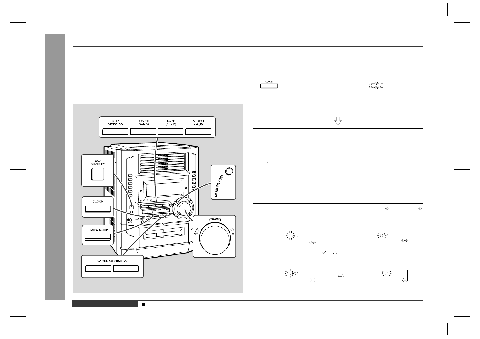
CD-BK3200V
– 40 –
Figure 40 WIRING SIDE OF P.W.BOARD (2/11)
A
B
C
D
E
F
G
H
1
23456
R619
R614
C388
R378
R373
R372
R374
123456789
10 11
1213141516171819202122
123456789
10 11
12
13141516171819202122
R388
R376
R359
C395
R360
C387
R379
C386
C392
TP301
TP301
TP302
R377
R385
R395
R393
C385
C318
R380
R383
C324
R327
R302
C311
C351
C310
C356
C313
C350
C312
C354
R353
R355
C353
R352
C355
C399
C309
C308
R311
C366
R351
R313
R365
C316
C369
C334
R350
C361
R356
R323
C342
C363
C332
C335
R618
R613
R617
R607
R611
R606
R605
C604
R637
R638
1
2
R626
R625
C637
R623
R624
C631
R633
R631
C632
R632
R634
C338
C330
R336
C323
R316
C317
C314
C303
C304
C315
C305
1
2
3
4
5
6
7
8
9
R325
R322
C306
R381
C397
C301
C381
C382
C384
C634
VD302
VD303
VD301
SW601
SPAN
SELECTOR
100 kHz/10 kHz
50 kHz/9 kHz
BK
WH
1
2
SO302
FM
ANTENNA
TERMINAL
JK601
VIDEO/AUX
IN
R-CH
L-CH
AM LOOP
ANTENNA
FM
75 OHMS
GND
1
2
TO VIDEO CD PWB
P47 11-A
JK671
VIDEO OUT
2324
TO POWER AMP. PWB
P45 12-D
MAIN PWB-A
1
2
3
TO
VIDEO CD PWB
P47 10-A
123456
RD
WH
BL
WH
BL
WH
CNS601
CNP8
C
N
CNP906
123456789
C625
C621
C617
C613
R612
R609
R610
R608
C372
C374
C373
C358
ZD351
L352
C654
X352
IC302
C396
R387
R386
R384
L351
C391
C380
R391
R392
R375
C393
Q360
R382
T301
Q302
T351
CF352
C398
C370
C352
CF351
T302
R309
C357
CF303
IC303
D305
X351
C371
C367
C362
R358
C368
R357
C365
C364
T306
R641
R643
R642
Q604
R615
R616
Q603
C602
C614
C606
C611
C620
C607
C610
C608
C622
C609
C612
C624
IC601
C626
C629
C623
C628
C630
C619
C627
D604
D603
R601
D602
D601
C331
T303
D302
BF301
D301
CNP301
L312
2 1
R314
IC301
C307
C320
C394
BI602
1
2
3
4
5
6
7
8
9
10
11
14
12
13
15
16
17
18
19
20
21
22
23
24
B C E
B C E
B C E
B
C
E
1 2 3
3
2
1
CNS602
CNP10