CD-E700H
No. S2313CDE700H/
CONTENTS
Page
SAFETY PRECAUTION FOR SERVICE MANUAL ........................................................................................................... 2
SPECIFICATIONS ............................................................................................................................................................. 3
NAMES OF PARTS ........................................................................................................................................................... 4
DISASSEMBLY .................................................................................................................................................................. 6
REMOVING AND REINSTALLING THE MAIN PARTS ..................................................................................................... 9
ADJUSTMENT ................................................................................................................................................................. 10
NOTES ON SCHEMATIC DIAGRAM .............................................................................................................................. 14
TYPES OF TRANSISTOR AND LED............................................................................................................................... 14
BLOCK DIAGRAM ........................................................................................................................................................... 15
SCHEMATIC DIAGRAM / WIRING SIDE OF P.W.BOARD ............................................................................................. 18
VOLTAGE ........................................................................................................................................................................ 35
WAVEFORMS OF CD CIRCUIT ...................................................................................................................................... 36
TROUBLESHOOTING ..................................................................................................................................................... 37
FUNCTION TABLE OF IC................................................................................................................................................ 41
REPLACEMENT PARTS LIST/EXPLODED VIEW
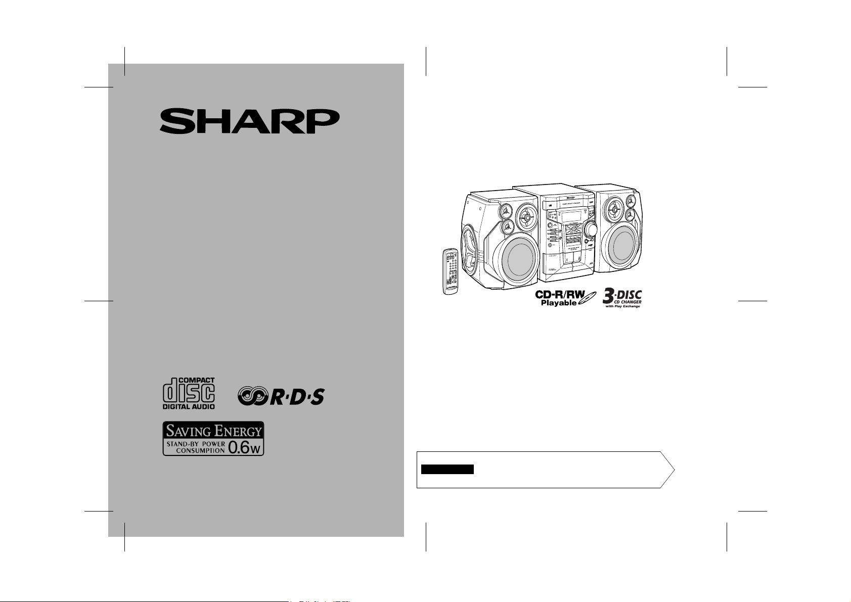
SERVICE MANUAL
This document has been published to be used
for after sales service only.
The contents are subject to change without notice.
SHARP CORPORATION
• In the interests of user-safety the set should be restored to its
original condition and only parts identical to those specified be
used.
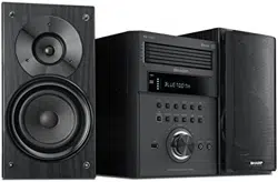
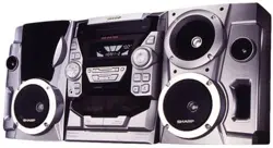
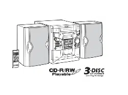
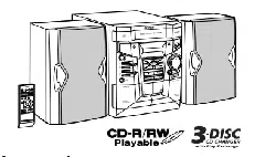
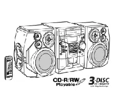
MINI COMPONENT SYSTEM
MODEL CD-E700H
CD-E700H Mini Component System consisting of CD-E700H
(main unit) and CP-E700H (speaker system).

CD-E700H
– 2 –
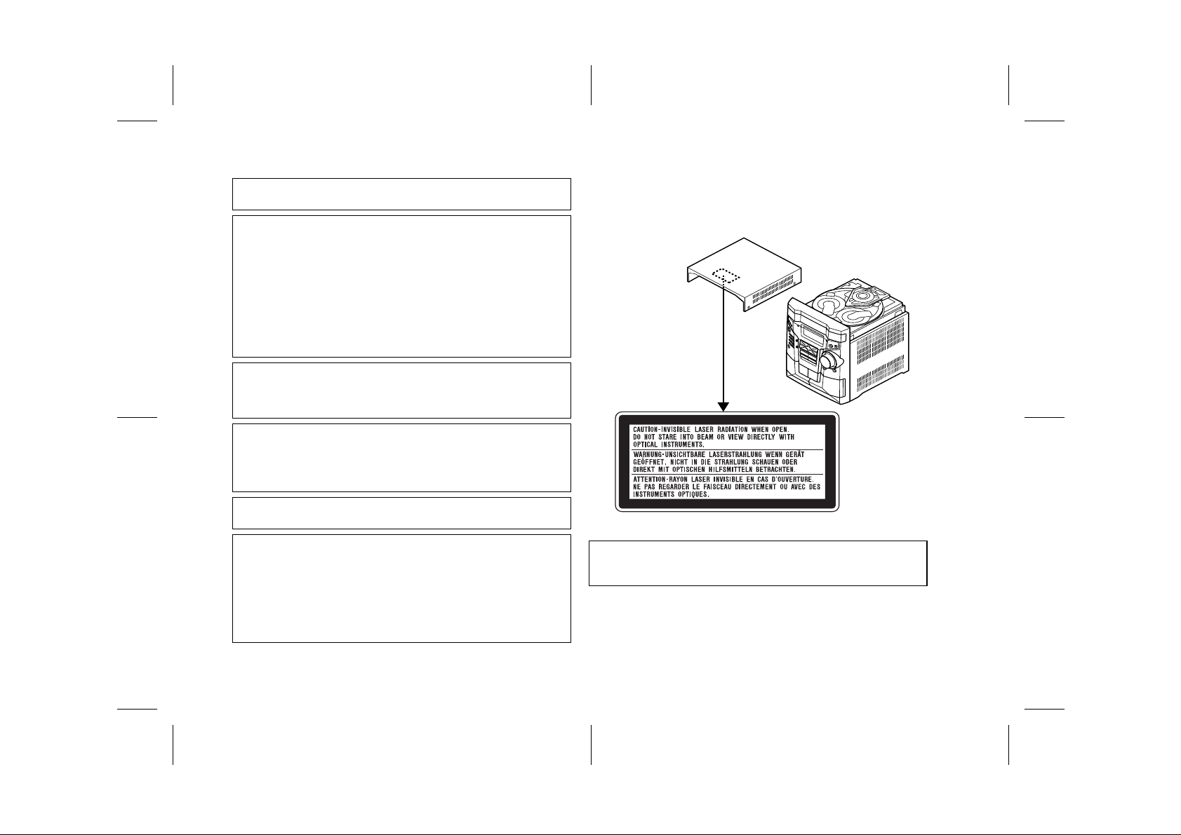
SAFETY PRECAUTION FOR SERVICE MANUAL
Precaution to be taken when replacing and servicing the Laser Pickup.
The AEL (Accessible Emission Level) of Laser Power Output for this model is specified to be lower than Class 1 Requirements.
However, the following precautions must be observed during servicing to protect your eyes against exposure to the Laser beam.
(1) When the cabinet has been removed, the power is turned on without a compact disc, and the Pickup is on a position outer than
the lead-in position, the Laser will light for several seconds to detect a disc. Do not look into the Pickup Lens.
(2) The Laser Power Output of the Pickup inside the unit and replacement service parts have already been adjusted prior to shipping.
(3) No adjustment to the Laser Power should be attempted when replacing or servicing the Pickup.
(4) Under no circumstances look directly into the Pickup Lens at any time.
(5) CAUTION - Use of controls or adjustments, or performance of procedures other than those specified herein may result in
hazardous radiation exposure.
Laser Diode Properties
Material: GaAIAs
Wavelength: 780 nm
Emission Duration: continuous
Laser Output: max. 0.6 mW
VAROITUS! LAITTEEN KÄYTTÄMINEN MUULLA KUIN TÄSSÄ
KÄYTTÖOHJEESSA MAINITULLA TAVALLA SAATTAA
ALTISTAA KÄYTTÄJÄN TURVALLISUUSLUOKAN 1
YLITTÄVÄLLE NÄKYMÄTTÖMÄLLE LASERSÄTEILYLLE.
VARNING - OM APPARATEN ANVÄNDS PÅ ANNAT SÄTT ÄN
I DENNA BRUKSANVISNING SPECIFICERAS. KAN
ANVÄNDAREN UTSÄTTAS FÖR OSYNLIG LASER-
STRÅLNING, SOM ÖVERSKRIDER GRÄNSEN FÖR
LASERKLASS 1.
ADVERSEL-SYNLIG OG USYNLIG LASERSTRÅLING VED ÅBNING.
SE IKKE IND I STRÅLEN-HELLER IKKE MED OPTISKE INSTRUMENTER.
VARO! AVATTAESSA OLET ALTTIINA NÄKYVÄLLE JA NÄKYMÄTTÖMÄLLE
LASERSÄTEILYLLE ÄLÄ TUIJOTA SÄTEESEEN ÄLÄKÄ KATSO SITÄ
OPTISEN LAITTEEN LÄPI.
VARNING-SYNLIG OCH OSYNLIG LASERSTRÅLNING NÄR DENNA
DEL ÄR ÖPPNAD. STIRRA EJ IN I STRÅLEN OCH BETRAKTA EJ
STRÅLEN GENOM OPTISKT INSTRUMENT.
– 3 –
CD-E700H
SPECIFICATIONS
CD-E700H
Specifications for this model are subject to change without
prior notice.
FOR A COMPLETE DESCRIPTION OF THE OPERATION OF THIS UNIT, PLEASE REFER
TO THE OPERATION MANUAL.
CP-E700H
General
Amplifier
Power source AC 230 V, 50 Hz
Power
consumption
Power on: 110 W
Power stand-by: 0.6 W (*)
Dimensions Width: 270 mm (10-5/8")
Height: 330 mm (13")
Depth: 355 mm (13-15/16")
Weight 7.8 kg (17.2 lbs.)
( * )This power consumption value is obtained when the demonstra-
tion mode is cancelled in the power stand-by mode.
Output power PMPO: 940 W
MPO: 470 W (235 W + 235 W) (DIN 45 324)
RMS: 250 W (125 W + 125 W) (DIN 45 324)
RMS: 200 W (100 W + 100 W) (DIN 45 500)
Output terminals Speakers: 6 ohms
Headphones: 16 - 50 ohms (recommended:
32 ohms)
Input terminals Video/Auxiliary (audio signal): 500 mV/47 k
ohms
CD player
Tuner
Cassette deck
Type 3-disc multi-play compact disc player
Signal readout Non-contact, 3-beam semiconductor laser
pickup
D/A converter 1-bit D/A converter
Frequency
response
20 - 20,000 Hz
Dynamic range 90 dB (1 kHz)
Frequency range FM: 87.5 - 108 MHz
AM: 522 - 1,620 kHz
Frequency
response
50 - 14,000 Hz (normal tape)
Signal/noise ratio 55 dB (TAPE 1, playback)
50 dB (TAPE 2, recording/playback)
Wow and flutter 0.35 % (DIN 45 511)
Type 3-way 4-speaker system with passive radia-
tor
Super tweeter 2
5 cm (2") tweeter
16 cm (6-1/2") woofer
16 cm (6-1/2") passive radiator
Maximum input
power
250 W
Rated input power 125 W
Impedance 6 ohms
Dimensions Width: 277 mm (10-7/8")
Height: 330 mm (13")
Depth: 273 mm (10-3/4")
Weight 4.5 kg (9.9 lbs.)/each
CD-E700H
– 4 –
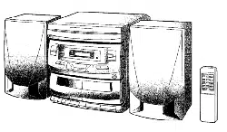
NAMES OF PARTS
CD-E700H
Front panel
1. Disc Tray
2. Timer Set Indicator
3. RDS Display Mode Select Button
4. RDS ASPM (Auto Station Programme Memory) Button
5. RDS Programme Type/
Traffic Information Search Button
6. Memory/Set Button
7. On/Stand-by Button
8. Clock Button
9. Timer/Sleep Button
10. Tuning and Time Up Button
11. Tuning and Time Down Button
12. Headphone Socket
13. Tape 2 Record Pause Button
14. Tape 1 Cassette Compartment
15. Equaliser Mode Select Button
16. Extra Bass/Demo Mode Button
17. Volume Control
18. Disc Tray Open/Close Button
19. Disc Skip Button
20. Tape 2 Cassette Compartment
21. CD Button
22. Tape (1 2) Button
23. CD or Tape Stop Button
24. CD Track Down or Fast Reverse, Tape 2 Rewind,
Tuner Preset Down Button
25. Tuner (Band) Button
26. Video/Auxiliary Button
27. CD Play or Repeat, Tape Play Button
28. CD Track Up or Fast Forward, Tape 2 Fast Forward,
Tuner Preset Up Button
6
7
8
2
1
9
11
12
13
14
10
15
19
17
18
20
16
25
26
27
28
21
22
23
24
3
4
5
Display
1. CD Pause Indicator
2. Extra Bass Indicator
3. Disc Number Indicators
4. Tape 2 Record Indicator
5. FM Stereo Mode Indicator
6. FM Stereo Receiving Indicator
7. Timer Play Indicator
8. Sleep Indicator
9. Timer Recording Indicator
10. CD Play Indicator
11. CD Repeat Play Indicator
12. RDS Indicator
13. Dynamic PTY Indicator
14. Tape Play Indicator
15. Traffic Programme Indicator
16. Traffic Announcement Indicator
17. Memory Indicator
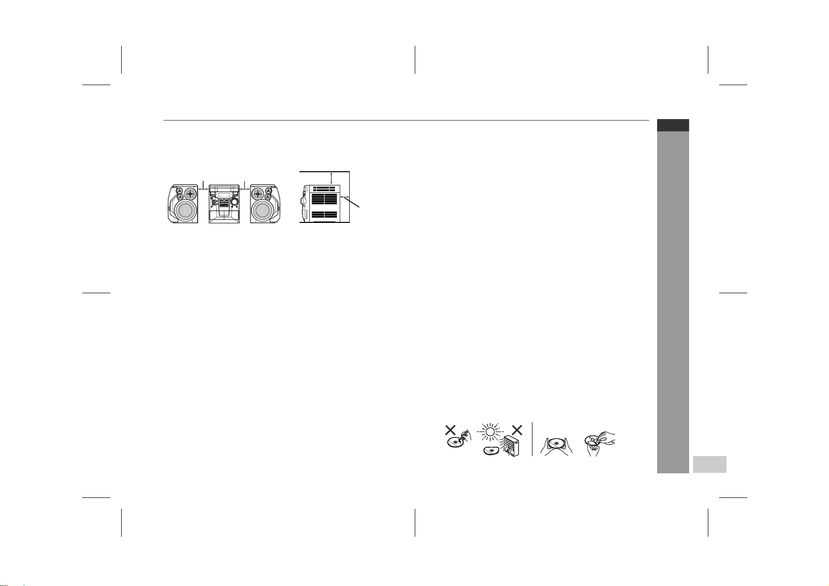
Rear panel
1. Cooling Fan
2. AC Power Lead
3. FM 75 Ohms Aerial Socket
4. AM Loop Aerial Socket
5. Video/Auxiliary (Audio Signal) Input Sockets
6. Speaker Terminals
Note:
This product is equipped with a cooling fan inside, which begins to
run at a specified volume level for better heat radiation.
2
1
5
6
4
3
14 17
23456791 8
12
10
11
13
15 16
– 5 –
CD-E700H
Remote control
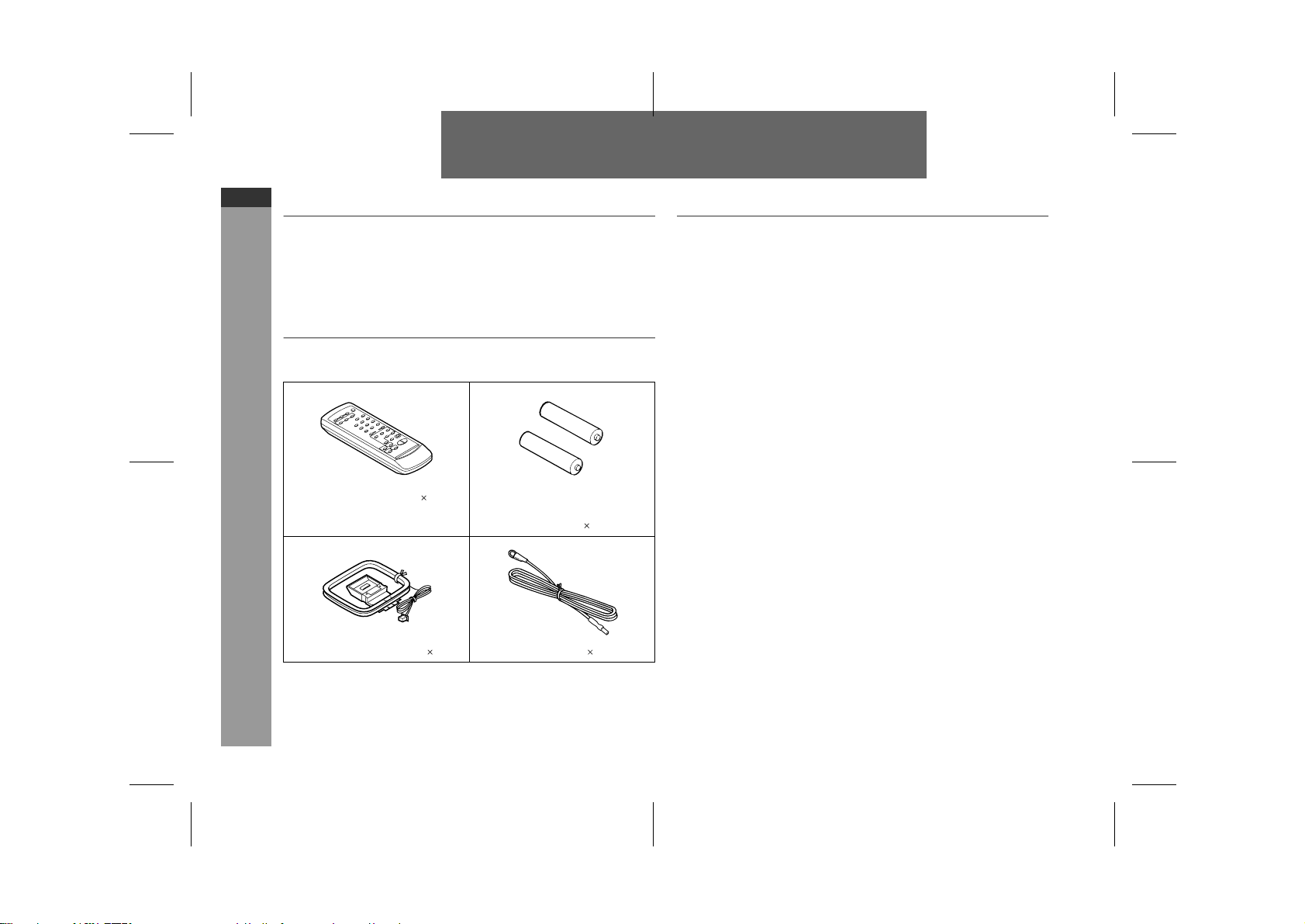
1. Remote Control Transmitter
2. Disc Number Select Buttons
3. Programme Clear Button
4. CD Memory Button
5. CD Track Down or Fast Reverse,
Tape 2 Rewind Button
6. CD Pause Button
7. CD or Tape Stop Button
8. Tape 2 Record Pause Button
9. CD Button
10. Tape (1 2) Button
11. On/Stand-by Button
12. CD Random Button
13. Direct Search Buttons
14. Tuner Preset Up and Down Buttons
15. CD Track Up or Fast Forward,
Tape 2 Fast Forward Button
16. CD Play or Repeat, Tape Play Button
17. Extra Bass Button
18. Equaliser Mode Select Button
19. Volume Up and Down Buttons
20. Tuner (Band) Button
21. Video/Auxiliary Button
Buttons with " " mark in the illustration or highlighted in bold on the
right can be operated on the remote control only.
1
2
4
5
6
7
8
9
10
14
11
3
12
13
17
18
19
20
21
15
16
1. Super Tweeters
2. Woofer
3. Tweeter
4. Passive Radiator
5. Speaker Wire
1
4
3
5
2
CD-E700H
CP-E700H
CD-E700H
– 6 –
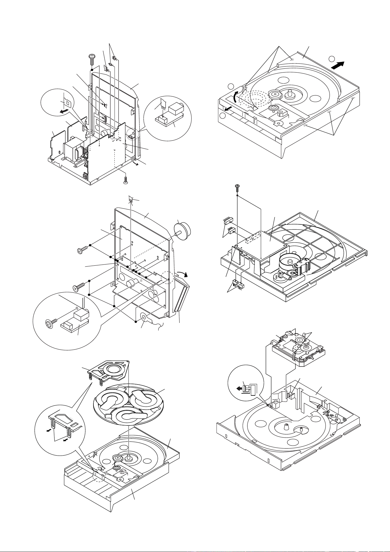
1 Top Cabinet 1. Screw ...................... (A1) x4 6-1
2 Side Panel 1. Screw ...................... (B1) x8 6-1
(Left/Right)
3 CD Tray Cover/ 1. Turn on the power supply, .. 6-2
CD Player Unit open the disc tray, take out
the CD tray cover, and close.
(Note 1)
2. Screw ...................... (C1) x1
3. Hook ........................ (C2) x3
4. Hook ........................ (C3) x2
5. Socket ..................... (C4) x2
4 Rear Panel with 1. Screw ...................... (D1) x8 6-2
Fan Motor 2. Socket ..................... (D2) x1
5 Main PWB 1. Screw ...................... (E1) x4
6-2, 7-1
2. Socket ..................... (E2) x3 7-1
3. Flat Cable ............... (E3) x1
4. Flat Wire.................. (E4) x1
6 Front Panel 1. Screw .......................(F1) x1 7-1
2. Hook .........................(F2) x2
3. Flat Wire...................(F3) x1
7 Display PWB 1. Knob ........................ (G1) x1 7-2
2. Screw .................... (G2) x10
3. Flat Cable ............... (G3) x1
8 Tape Mechanism 1. Open the cassette holder. .. 7-2
2. Screw...................... (H1) x5
9
Headphones PWB
1. Screw ....................... (J1) x1 7-2
10 Turntable 1. Hook ........................ (K1) x2 7-3
2. Cover ...................... (K2) x1
11 Loading Tray 1.
Turn fully the lock lever in the
6-3
arrow direction
.
2.
Push the loading tray backward
7-4
to engage the claw with the
groove and remove it in the
direction of the arrow
...
(L1) x6
12 CD Servo PWB 1. Screw ...................... (M1) x2 7-5
(Note 2) 2. Hook ........................ (M2) x1
3. Socket ..................... (M3) x4
13 CD Mechanism 1. Hook ........................ (N1) x2 7-6
2. Hook ........................ (N2) x2
DISASSEMBLY
Caution on Disassembly
Follow the below-mentioned notes when disassembling
the unit and reassembling it, to keep it safe and ensure
excellent performance:
1. Take cassette tape and compact disc out of the unit.
2. Be sure to remove the power supply plug from the wall
outlet before starting to disassemble the unit.
3. Take off nylon bands or wire holders where they need to
be removed when disassembling the unit. After servicing
the unit, be sure to rearrange the leads where they were
before disassembling.
4. Take sufficient care on static electricity of integrated
circuits and other circuits when servicing.
Figure 6-2
STEP
REMOVAL PROCEDURE FIGURE
Figure 6-1
Note 1: How to open the changer manually. (Fig. 6-3)
1. In this state, turn fully the lock lever in the arrow direction through
the hole on the loading tray bottom.
2. After that, push forward the Loading tray.
Note 2:
1. After removing the connector for the optical pickup from the
connector, wrap the conductive aluminium foil around the front end
of the connector so as to protect the optical pickup from electro-
static damage.
Note 3:
1. Be careful not to break the claw of the CD mechanism.
2. When fining back the cam gear assembly, let it lock by front
movement.
(B1)x2
ø3x10mm
(A1)x2
ø3x12mm
(A1)x2
ø3x12mm
(B1)x2
ø3x10mm
(B1)x4
ø3x10mm
Rear
Panel
Side Panel
(Right)
Side Panel
(Left)
Top Cabinet
Front
Panel
(C3)x1
CD Player
Unit
CD Tray Cover
(C2)x3
1
1
2
2
(E1)x1
ø3x10mm
(C1)x1
ø3x10mm
(E1)x1
ø3x10mm
(D1)x1
ø3x10mm
Lug Wire
Main PWB
Rear
Panel
Fan
Motor
Pull
(C3)x1
(C4)x2
CD Servo
PWB
Main
PWB
(D2)x1
(D1)x7
ø3x10mm
Figure 6-3
Lock Lever
CD Player Unit
(Bottom View)
CD-E700H
CD-E700H
– 7 –
CD-E700H
Figure 7-1
Figure 7-2
Figure 7-3
Figure 7-4
Figure 7-5
Figure 7-6
(F1)x1
ø3x10mm
Headphones
PWB
(E4)x1
Front
Panel
(E1)x2
ø3x6mm
(F2)x1
(F2)x1
(E2)x1
(F3)x1
(E3)x1
(E2)x2
Main PWB
Transformer
PWB
Power PWB
(G3)x1
Display PWB
Open
Cassette
Holder
Tape
Mechanism
(H1)x5
ø3x10mm
Lug Wire
Front Panel
Headphones
PWB
(J1)x1
ø3x10mm
(G2)x10
ø3x10mm
(G1)x1
CD Player Unit
Loading
Tray
(K2)x1
(K1)x2
Turntable
(L1)x3
3
(L1)x3
Loading Tray
1
2
Loading
Tray
(M1)x2
ø3x10mm
(M3)x2
CD Servo
PWB
(M2)x1
(M3)x2
CD
Mechanism
(N2)x2
(N1)x1
(N1)x1
Loading Tray
CD-E700H
– 8 –
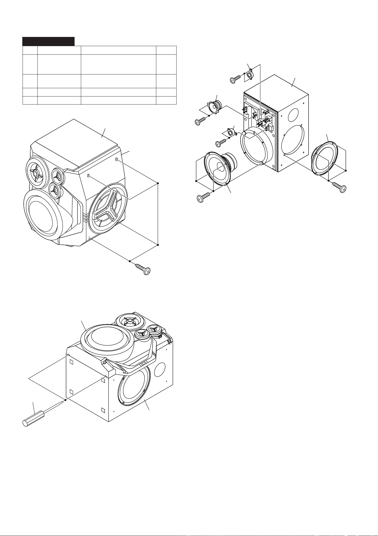
Figure 8-1
Figure 8-3
1 Passive Radiator 1. Screw ...................... (A1) x4 8-1
2. Side Panel .............. (A2) x1
3. Screw ...................... (A3) x4 8-3
2 Woofer 1. Front Panel ............. (B1) x1 8-2
2. Screw ...................... (B2) x4 8-3
3 Tweeter 1. Screw ...................... (C1) x2 8-3
4 Super Tweeter 1. Screw ...................... (D1) x4 8-3
STEP
REMOVAL PROCEDURE FIGURE
(A3)x4
ø4x16mm
(B2)x4
ø4x16mm
(D1)x2
ø3x12mm
(C1)x2
ø3x12mm
(D1)x2
ø3x12mm
Speaker Box
Woofer
Tweeter
Super Tweeter
Super Tweeter
Passive
Radiator
(A1)x4
ø4x40mm
Speaker Box
(A2)x1
Screwdriver
Driver should
be pried away
from Speaker Box.
(B1)x1
Speaker Box
Figure 8-2
CP-E700H
– 9 –
CD-E700H
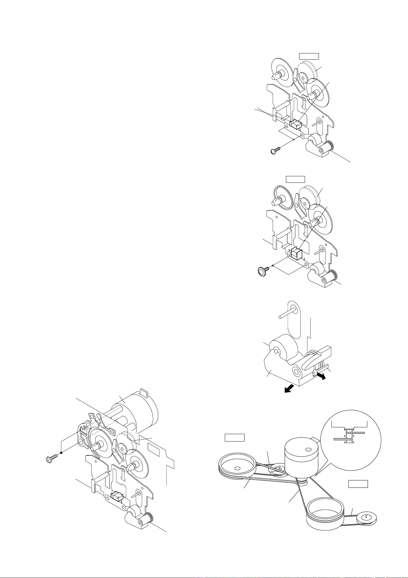
REMOVING AND REINSTALLING THE MAIN PARTS
TAPE MECHANISM SECTION
Perform steps 1 to 6 and 8 of the disassembly method to
remove the tape mechanism.
How to remove the record/playback and erase
heads (TAPE 2) (See Fig. 9-1)
1. When you remove the screws (A1) x 2 pcs., the recording/
playback head and three-dimensional head of the erasing
head can be removed.
How to remove the playback head (TAPE 1)
(See Fig. 9-2)
1. When you remove the screws (B1) x 2 pcs., the playback
head can be removed.
How to remove the pinch roller (TAPE 1/2)
(See Fig. 9-3)
1. Carefully bend the pinch roller pawl in the direction of the
arrow <A>, and remove the pinch roller (C1) x 1 pc., in the
direction of the arrow <B>.
Note:
When installing the pinch roller, pay attention to the spring
mounting position.
How to remove the belt (TAPE 2)
(See Fig. 9-4)
1. Remove the main belt (D1) x 1 pc., from the tape motor side.
2. Remove the FF/REW belt (D2) x 1 pc.
How to remove the belt (TAPE 1)
(See Fig. 9-4)
1. Remove the main belt (E1) x 1 pc., from the tape motor side.
2. Remove the FF/REW belt (E2) x 1 pc.
How to remove the motor (See Fig. 9-5)
1. Remove the screws (F1) x 2 pcs., to remove the tape motor.
Figure 9-1
Figure 9-2
Figure 9-3
Figure 9-4Figure 9-5
(A1)x2
Ø2x6mm
TAPE 2
Record/Playback
Head
Erase Head
Clutch Ass'y
(B1)x2
Ø2x9mm
TAPE 1
Playback
Head
Clutch Ass'y
Pinch Roller
(C1)x1
<A>
<B>
Pinch
Roller
Pawl
Pull
TAPE 2
TAPE 1
Main Belt
(E1)x1
TAPE 2
Main Belt
(D1)x1
TAPE 1
Main Belt
(D1)x1
Main Belt
(E1)x1
FF/REW
Belt
(D2)x1
FF/REW
Belt
(E2)x1
Tape
Motor
Tape
Motor
(F1)x2
Ø2.6x5mm
Tape
Motor
Clutch Ass'y

CD-E700H
– 10 –
How to remove the pickup unit (See Fig. 10-2)
1. Remove the stop washer (B1) x 1 pc., to remove the gear
(B2) x 1 pc.
2. Remove the screws (B3) x 2 pcs., to remove the shaft
(B4) x 1 pc.
3. Remove the pickup.
Note
After removing the connector for the optical pickup from the
connector wrap the conductive aluminium foil around the front
end of connector so as to protect the optical pickup from
electrostatic damage.
Figure 10-2
CD MECHANISM SECTION
Perform steps 1, 2, 3, 10, 11, 12 and 13 of the disassembly
method to remove the CD mechanism.
How to remove the loading motor
(See Fig. 10-1)
1. Bend the hooks (A1) x 5 pcs., to remove the loading motor.
Figure 10-1
ADJUSTMENT
MECHANISM SECTION
••
••
• Driving Force Check
Torque Meter Specified Value
Play: TW-2111 Tape 1: Over 80 g
Tape 2: Over 80 g
••
••
• Torque Check
Torque Meter
Tape 2
Play: TW-2111 30 to 80 g.cm 30 to 80 g.cm
Fast forward: TW-2231 — 70 to 180 g.cm
Rewind: TW-2231 — 70 to 180 g.cm
Specified Value
Tape 1
Specified
Value
Adjusting
Point
Instrument
Connection
Test Tape
Normal MTT-111 Variable 3,000 ± 30 Hz Speaker
speed Resistor in Terminal
motor. (Load
resistance:
6 ohms)
••
••
• Tape Speed
Figure 10-3
(B3)x2
ø2.6x6mm
Shaft
(B4)x1
Stop Washer
(B1)x1
Gear
(B2)x1
CD Mechanism
Pickup
Unit
TAPE MECHANISM
Tape
Motor
Variable Resistor in motor
(A1)x5
Loading
Motor PWB
Loading
Motor
Loading
Tray
– 11 –
CD-E700H
Figure 11-2
CD ERROR CODE DESCRIPTION
Error Explanation
01
When Pickup set inner position, inner switch
cannot detect 'ON' level for 10 secs.
When tray moves to Open/Close, Open/Close switch
10*
cannot detect 'ON' level for 7 secs.
When disc table rotate to target position.
Clamp switch cannot detect 'ON' level for 7 secs.
When disc table set to Disc1 position for 1 st time,
11* "CLAMP SW", "DISC NO SW" and "OPEN/CLOSE"
cannot detect 'ON' level for 14 secs.
31
When it changes to CD function, DSP cannot read
initial data.
T
T
EFBL
FDO
TE
Stopped
CH1=500 mV
DC 10:1
CH2=200 mV
DC 10:1
CH3=1 V
DC 10:1
500 ms/div
(500 ms/div)
NORM:20 kS/s
1
2
3
=Record Length=
Smoothing : ON CH1 : 0.000 V
CH2 : 0.000 V
Main : 100K
Zoom : 2k
Mode : SINGLE
Type : EDGE CH1
Delay : 0.0 ns
Hold off : 0.2 µs
CH3 : 0.00 V
CH4 : 0.00 V
BW : FULL
=Trigger==Filter= =Offset=
CH2
v/DIV
200 mV
1999/04/05 20:26:47
CD SECTIONTUNER SECTION
fL: Low-range frequency
fH: High-range frequency
Items adjusted automatically
(1) Offset adjustment (The offset voltage between the head
amplifier output and the VREF reference voltage is
compensated inside the IC.)
* Focus offset adjustment
* Tracking offset adjustment
(2) Tracking balance adjustment (waveform drawing
Fig.11-2 EFBL)
(3) Gain adjustment (The gain is compensated inside the IC
so that the loop gain at the gain crossover frequency will
be 0 dB.)
* Focus gain adjustment
* Tracking gain adjustment
• Adjustment
Since this CD system incorporates the following automatic
adjustment functions, readjustment is not needed when
replacing the pickup. Therefore, different PWBs and pickups
can be combined freely.
Each time a disc is changed, these adjustments are
performed automatically. Therefore, playback of each disc
can be performed under optimum conditions.
* 'CHECKING'
If Error is detected, 'CHECKING' will be display instead of 'ER-
CD**' display. 'ER-CD**' display will only be display when
error had been detected for the 5 th times.
Figure 11-1 ADJUSTMENT POINTS
Test Stage
Frequency Frequency
Display
Setting/
Adjusting
Parts
Instrument
Connection
••
••
•
AM IF/RF
Signal generator: 400 Hz, 30%, AM modulated
*1. Input: Antenna Output: TP302
*2. Input: Antenna Output: TP301
AM IF 450 kHz 1,620 kHz T351 *1
AM Band — 522 kHz (fL): T306 *2
Coverage 1.1 ± 0.1 V
AM Tracking 990 kHz 990 kHz (fL): T303 *1
SO301
FM ANTENNA
TERMINAL
AM IF
TP301
TP302
R357
R381
T303
T306
L354
FE301
T351
CNP302
AM LOOP
ANTENNA
AM BAND
COVERAGE fL
AM TRACKING
fL
MAIN PWB
1
• FM IF
Notes:
1: Description of the "FM IF Adjustment" is not carried on this
Manual. It is because the IF coil in the FM front end section
has been best adjusted in the factory so that its further
adjustment is not needed at the field. When replacing the
FM front end assembly, no adjustment is needed either.
2: The parts in the FM front end section are prepared in a
complete unit, so you can't obtain each part individually.
CD-E700H
– 12 –
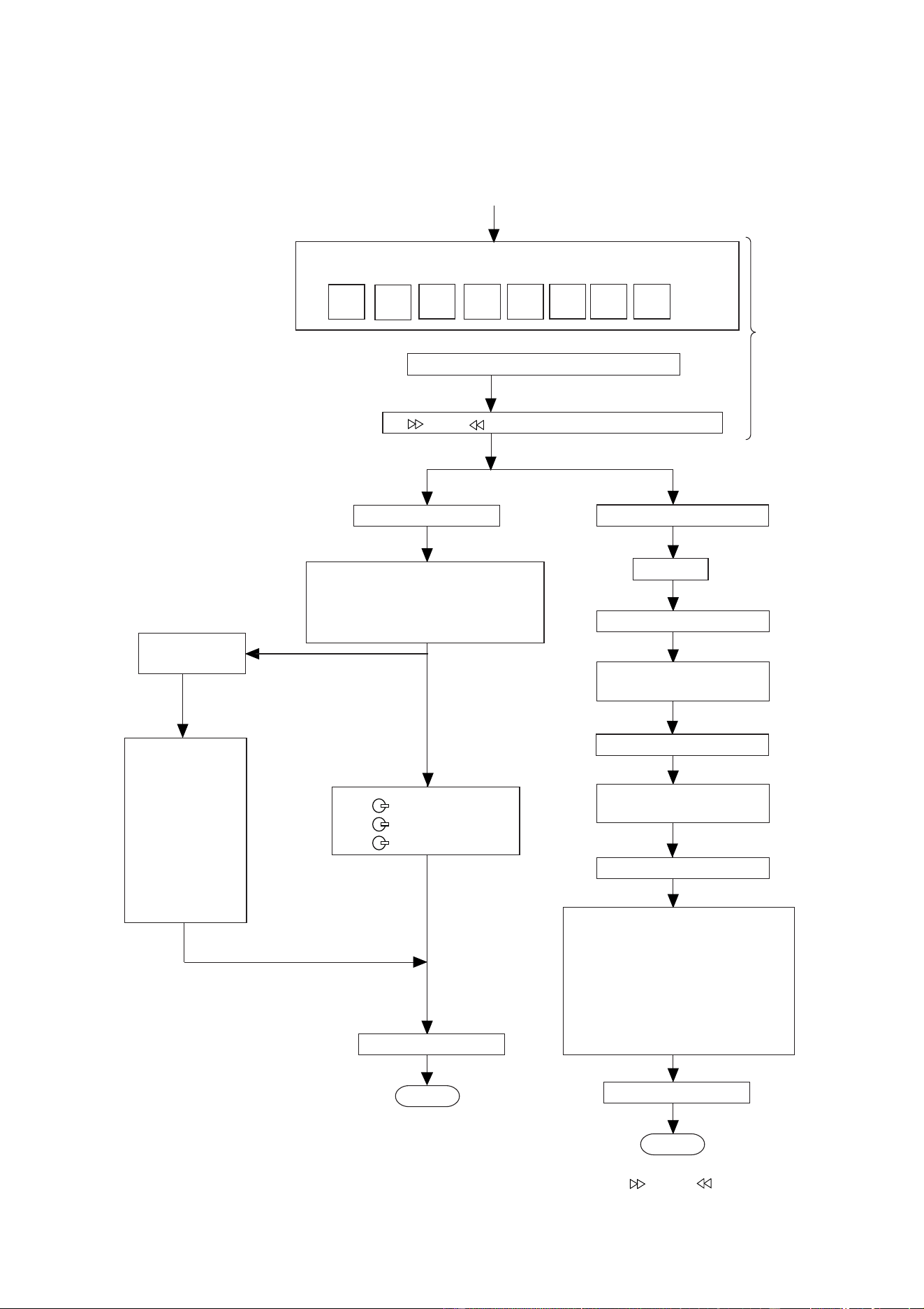
TEST MODE
• Setting the test mode
Any one of test mode can be set by pressing several keys as follows.
<X-BASS> + <CD> + <POWER> TEST: CD operation test.
Function: -CD test mode.
-Enter test mode.
C D T E S T
OPEN/CLOSE operation is using manual.
<< >>, << >> buttons make pick's slide possible.
Do TOC IL. Do normal play.
When these following key is input
into PLAY key, track number can
be appoint directly.
<<PLAY>> key input.
<<MEMORY>> key input.
<< 1 >> key: Track 4
<<
2>> key: Track 9
<<
3>> key: Track 15
<<STOP>> key input.
STOP
Laser ON.
<<MEMORY>> key input.
Tracking OFF play at that
specific point.
<<MEMORY>> key input.
Tracking ON play from
that specific point.
<<STOP>> key input.
STOP
IL isn't done
VOL — Last memory
BAL — CENTER
P.GEQ — FLAT
X-BASS — OFF
To cancel : Power OFF
Sliding the PICKUP with
<<
>>, << >> button
must only be in STOP mode.
<<MEMORY>>
key input.
Adjustment result
automatically will
display as below.
for each 2 sec :
a) "FOFF_XX"
b) "TOFF_XX"
c) "TBAL_XX"
d) "TGAN_XX"
f) "FGAN_XX"
g) "RFLS_XX"
explanation:
a) Focus off set = "FOFF_XX"
b) Tracking off set = "TOFF_XX"
c) Tracking balance = "TBAL_XX"
d) Tracking Gain = "TGAN_XX"
f) Focus Gain = "FGAN_XX"
g) RF level shift = "RFLS_XX"
Adjustment result automatically will
display as below for each 2 sec :
a) "FOFF_XX"
b) "TOFF_XX"
c) "TBAL_XX"
d) "TGAN_XX"
f) "FGAN_XX"
g) "RFLS_XX"
<<MEMORY>> key input.

– 13 –
CD-E700H
Standard Specification of Stereo System Error Message Display Contents
Error Contents DISPLAY Notes
CD Pickup Mechanism Error. 'ER-CD**' 01: PU-IN SW Detection NG.
CD Changer Mechanism Error. 'ER-CD**' 10: Changer Error.
(*) 11: Initial Error.
CD DSP Communication Error 'ER-CD**' 31: DSP COMMUNICATION ERROR
Focus Not Match. 'NO DISC'
TUN PLL Unlock. FM 87.5 MHz PLL Unlock.
(*) CHECKING:
If CD changer mechanism error is detected, 'CHECKING' will be display instead of 'ER-CD**' display 'ER-CD**' will only be display
when CD changer mechanism error had been detected for the 5 th times.
Speaker abnormal detection and +B PROTECTION display
In case speaker abnormal detection or +B PROTECTION had occured, it can be check by pressing 'POWER', 'VIDEO' and 'X-
BASS' key twice. Display will show "S** B**". S is referring to speaker abnormal detection and B is referring to +B PROTECTION.
** is in hex valve.
+B PROTECTION is condition when irregular process occur on power supply line.
BEFORE TRANSPORTING THE UNIT
The following process need to be taken after set tapering/parts replacement.
1. Press the Power On Button to enter Power Stand-by mode.
2. While pressing down the
button and the X-Bass/Demo button, press the Power button until "CLEAR AL" appears
3. While pressing down the
button and the X-Bass/Demo button , press the Power button until "WAIT"
"FINISHED" appears.
4. Unplug the AC cord and the unit is ready for transporting.
CD-E700H
– 14 –
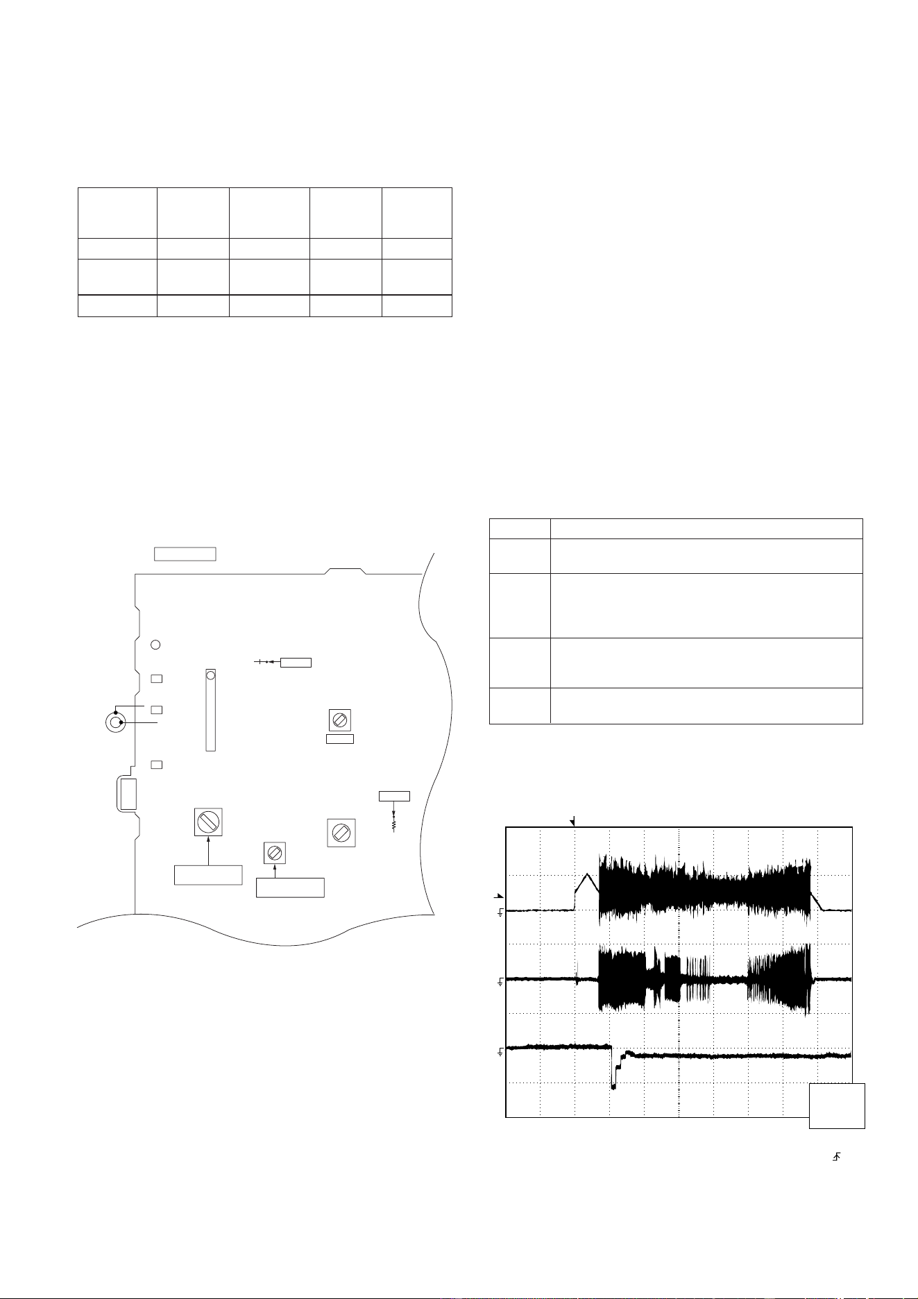
• The indicated voltage in each section is the one measured
by Digital Multimeter between such a section and the chas-
sis with no signal given.
1. In the tuner section,
indicates AM
indicates FM stereo
2. In the main section, a tape is being played back.
3. In the deck section, a tape is being played back.
( ) indicates the record state.
4. In the power section, a tape is being played back.
5. In the CD section, the CD is stopped.
• Parts marked with “ 1 ” ( ) are important for
maintaining the safety of the set. Be sure to replace these
parts with specified ones for maintaining the safety and
performance of the set.
NOTES ON SCHEMATIC DIAGRAM
• Resistor:
To differentiate the units of resistors, such symbol as K and
M are used: the symbol K means 1000 ohm and the symbol
M means 1000 kohm and the resistor without any symbol is
ohm-type resistor. Besides, the one with “Fusible” is a fuse
type.
• Capacitor:
To indicate the unit of capacitor, a symbol P is used: this
symbol P means pico-farad and the unit of the capacitor
without such a symbol is microfarad. As to electrolytic
capacitor, the expression “capacitance/withstand voltage”
is used.
(CH), (TH), (RH), (UJ): Temperature compensation
(ML): Mylar type
(P.P.): Polypropylene type
• Schematic diagram and Wiring Side of P.W.Board for this
model are subject to change for improvement without prior
notice.
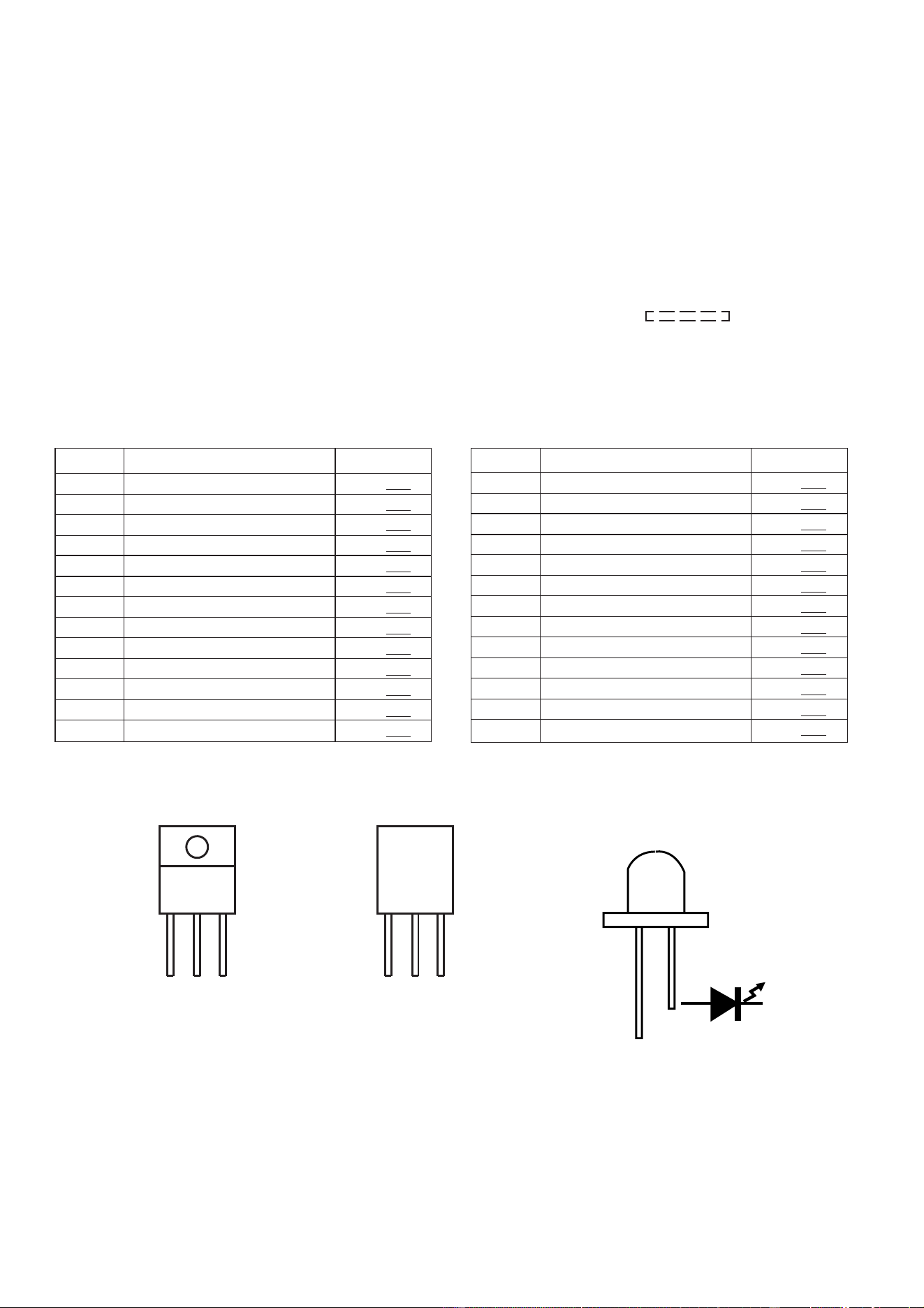
REF. NO DESCRIPTION POSITION
SW710
DISPLAY MODE
ON—OFF
SW711
CD
ON—OFF
SW712 TUNER ON—OFF
SW713 VIDEO/AUX ON—OFF
SW714 TAPE ON—OFF
SW715 STOP ON—OFF
SW716 PLAY ON—OFF
SW717 FAST FORWARD ON—OFF
SW718 FAST REWIND ON—OFF
SW721 X-BASS/DEMO ON—OFF
SW722 EQUALIZER ON—OFF
SW723 OPEN/CLOSE ON—OFF
SW724 DISC SKIP ON—OFF
SW1 OPEN/CLOSE ON—OFF
SW2 CLAMP ON—OFF
SW3 DISC NUMBER ON—OFF
SW4 PICKUP IN ON—OFF
SW701 ON/STAND-BY ON—OFF
SW702 MEMORY SET ON—OFF
SW703 REC/PAUSE ON—OFF
SW704 TUNING DOWN ON—OFF
SW705 TUNING UP ON—OFF
SW706
TIMER/SLEEP
ON—OFF
SW707
CLOCK
ON—OFF
SW708
PTY TI SEARCH
ON—OFF
SW709
ASPM
ON—OFF
TYPES OF TRANSISTOR AND LED
REF. NO
DESCRIPTION
POSITION
(1) (2) (3)
(S) (G) (D)
E C B B C E
FRONT
VIEW
FRONT
VIEW
KRA107 M
KRC102 M
KRC104 M
KTA1266 GR
KTA1273 Y
KTA1274 Y
304VT2E1
A503BC2E
KTC2026
FRONT
VIEW
KTA1271 Y
KTC3199 GR
KTC3200 GR
KTC3203 Y
2SC380 O
– 15 –
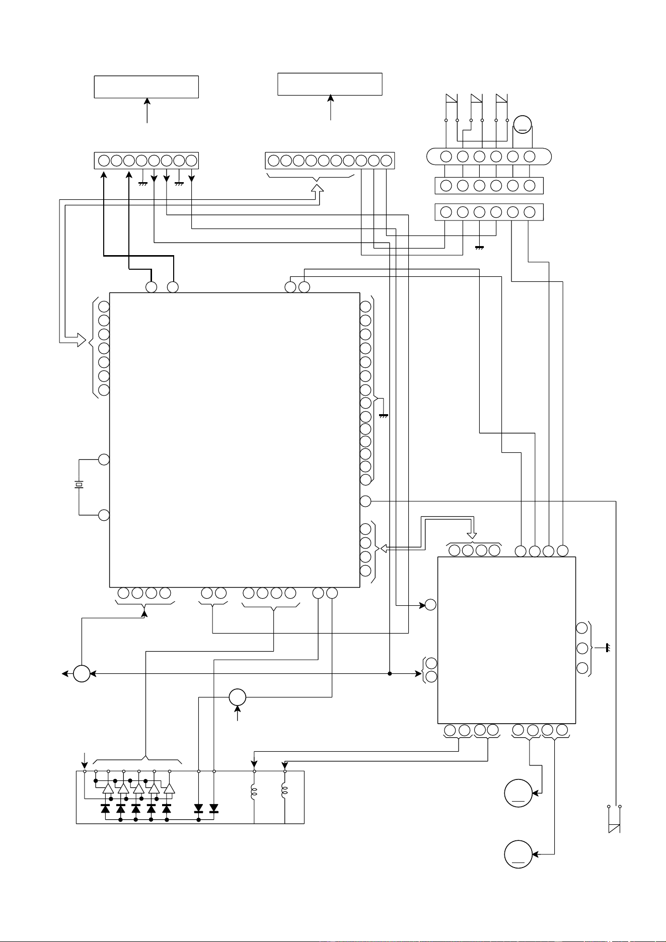
CD-E700H
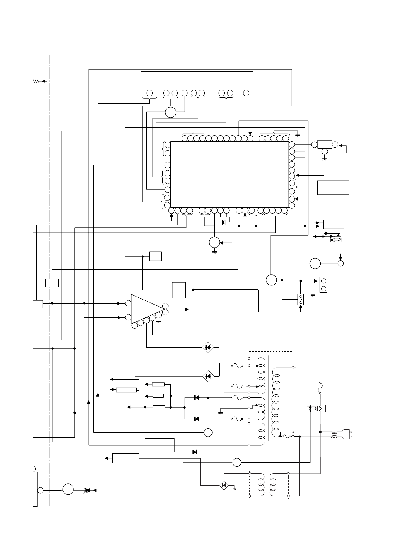
Figure 15 BLOCK DIAGRAM (1/3)
IC
80 79 77
71 70
47 46
45 42
41 18 10 9 8 7 5
CNP4
19
28
37
40
26
23
22
21
20
50
51
55
75
69
57
56
49
48
67
66
65
64
63
62
61
CONT 5
DRIVER
SPIN/SLED
FOCUS/TRACKING/
LA6574H
IC2
SPO
SLDO
FD
TO
VCC2
IC1
LC78646E
CD SERVO
LCHO
RCHO
CONT3
CONT2
SLDO
SPDO
FD0
TD0
LDD
LDS
TIN2
TIN1
FIN2
FIN1
RVDD
LVDD
XVDD
ADAVDD
VVDD
RFVDD
XIN
XOUT
DRF
VRES
VWRQ
DO
DI
CL
CE
TO DISPLAY SECTION
TO MAIN SECTION
BI4
CNP5
CNP6
SW3
DISC
NUMBER
SW2
CLAMP
SW1
OPEN/CLOSE
M3
T/T UP DOWN
LOADING MOTOR
D_GND
PICKUP UNIT
IN
PICKUP
SW4
MOTOR
SPINDLE
M1
MOTOR
SLED
M2
COIL
TRACKING
FOCUS COIL
16.9344 MHz
XL1
+6.5V
+5V
Q4
DRIVER
LASER
+3.3V
CONSTANT
VOLTAGE
+3.3V
+3.3V
Q1
+5V
R-CH
AGND
L-CH
D5V
WRQ
DRF
CE
DO
CL
DI
CLAMP SW
A5V
O/C,
CD RES
DISC NO
CNS4
+
–
+7V
(+B6)
(+B6)
(+B7)
29
12
22
1
15 13 1 7 24
28 27
3 2
30
26
9
10 11
8 7 6 5 4
8 7 1 2 3 4 5 6
10 3 1 9 8 7 6 52 4
2 3 1 4 6 5
2 3 1 4 6 5
2 3 1 4 6 5
6
43
M
M
M
44
DGND
CD-E700H
– 16 –
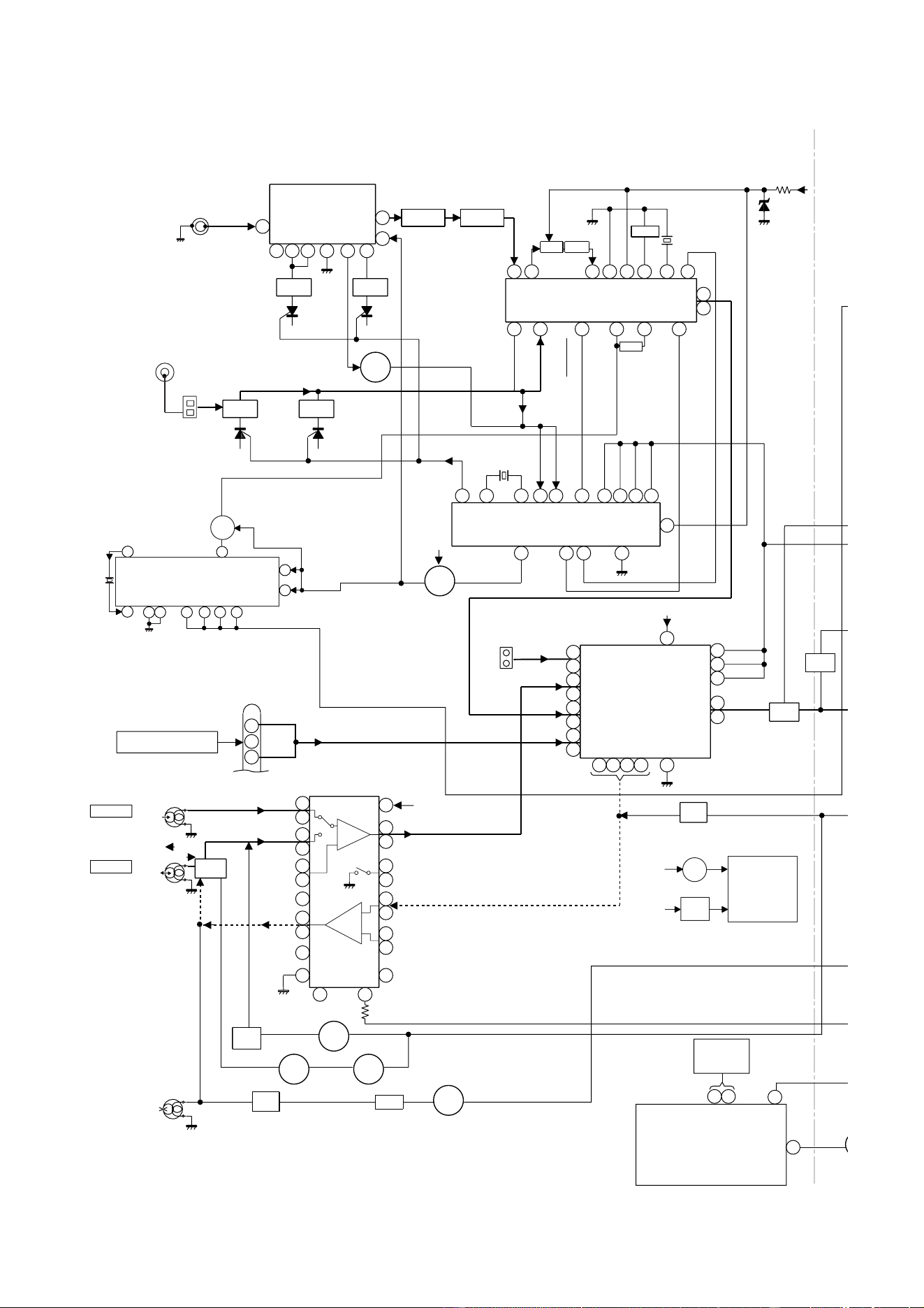
Figure 16 BLOCK DIAGRAM (2/3)
SO301
FM ANTENNA
TERMINAL
AM LOOP
ANTENNA
CNP302
IC101
AN7345K
PLAYBACK AND
RECORD
/PLAYBACK AMP.
R
L
R
L
JK690
VIDEO AUX IN
FM
+B
+B4
CLK
+B4
AM IF
OSC BUFF
FM IF
OSC
FM
BI601
ATT
–20dB
Q106
Q103-
Q108
Q107
Q602
Q601
X351
456 kHz
10.7 MHz
450 kHz
REC/PLAY
CLK
CE
DI
DO
DI
CE
MO/ST
SWITCHING
+B4
FM/AM
IC302
LC72131
PLL
(TUNER)
OU
FM/AM
L354
L
R
BIAS
T1
/
MUTING
SYSTEM
MUTE
P.B.
REC
AC BIAS
L
L
R
R
R
L
TAPE
TUNER
CD
P.B.
CNP5
FROM CD SECTION
HEAD
ERASE
SWITCHING
SWITCHING
SWITCHING
BIAS
Q113
Q114
Q112
Q110
SWITCHING
Q109
OSC.
BIAS
Q111
L103
Q105
Q106
REC./P.B. HEAD
TAPE 2
P.B. HEAD
TAPE 1
R-CH
L-CH
AUDIO PROCESSOR
LC75341
IC601
+B4
R
L
REC.
R
L
L NF
R NF
ALC
R REC.
REF
L REC.
POP REDUCE
R NF
L NF
SWITCHING
L(T2)
R(T2)
R(T1)
L(T1)
R
L
FM/AM
MPXIN
LOW PASS
FILTER
STEREO
AM RF IN
AM OSC. IN
FM
Q360
VT
OSC.
X352
4.5 MHz
COVERAGE
AM BAND
AM TRACKING
T303 T306
Q302
MO/ST VCO
DET
FMFM+BGND AM IF
CF351
FM/AM IF MPX.
IC303
LA1832S
FM IF DET./
FM MPX./AM IF
AM MIX
CF352
T351
RF
FM
OSC
FM
L312
T301
CF303T302
IC301
TA7358AP
FM FRONT END
4
22
3
24
2
1
81817
3
9
10
18
11
16
3
15
10
9
7
23
14
12
13
1
2
20
19
7
18
10
63
47
8
1 7
13
21
4
5
2
24
23
6
9
16
14
12
15
1
513
8432
1
21
7
985
17
6
21
21
20
22
11
17
15
9
6
57
13
14
12
15
16
23
4
7
H/N
P.B.
REC
T1/T2
T1/T2
HIGH
NOR/
416
21
R-CH
L-CH
Q706
Q707
Q708
TAPE
MECHANISM
ASS'Y
JOG701
JOG
VOLUME
MOTOR
DRIVER
SOLENOID
DRIVER
+B3
+B3
ICT21
LC72723
RDS DECORDER
16
15
14
13
8
9
10
2
3
11
7
MPX IN
VDDA
X OUT
X IN
QT21
XT21
4.332 MHz
RST
RDDA
RDCL
RD-ID/
READY
VSSD
TEST
VDDD
IC701
IX0553AW
SYSTEM
MICROCOMPUTER
(2/2)
D
Q
4950
Q604
Q603
– 17 –
CD-E700H
Figure 17 BLOCK DIAGRAM (3/3)
RL841
PT841
SUB POWER
TRANSFORMER
D842~
D845
IC854
AN78L05
+5.6V
+B5
+B PROTECT
+B7
+B2
D801
VL+
VL–
PT801
MAIN POWER
TRANSFORMER
F805
T2A L 250V
+B6
D803
D855
M12
IC851,IC852,IC853:
VOLTAGE
REGULATOR
IC855
+B3
KTC2026
Q905
KIA7812AP
KIA7810AP
D905
–VF
VF1
VF2
Q801
Q841
+5V
KIA7805AP
IC852
+B4
+B7
+B1
–B1
–B2
+B6
+B3
+B5
+B4
Q705
R
L
T
B
+B5
+B5
RX701
SENSOR
REMOTE
D804
D802
RL914
JK701
HEADPHONES
M901
FAN MOTOR
FAN MOTOR
DRIVER
SP RELAY
ON-OFF
SO901
SPEAKER
TERMINAL
M
Q906
Q709
Q904
Q901
Q903
Q902
D906
Q
602
Q
601
IC853
IC851
POWER AMP.
STK41242
IC901
A+10V
LD+7V
T2A L 250V
F803
T2A L 250V
F804
T4A L 250V
F801
T4A L 250V
F802
VH+
VH–
L-OUT
R-OUT
CLK
4.194304 MHz
RESET
MAIN
E
C/PLAY
VLOAD
RESET
GROUND
+B5
+B5
+B5
VDD
VDD
VDD
SP. DET.
-
CE
DI
DO
XL700
-
B
IAS
T1/T2
SYSTEM
MUTE
AVDD
SW721-SW724
SW701-SW718
KEY
SECTION
TO CD
T.F.
IC701
IX0553AW
SYSTEM
MICROCOMPUTER
(1/2)
FL DISPLAY
FL701
4514 19131125
79
91
86
92
85
70
38
37
34
35
63
31
33
29
41
87
6
1
11
7
8
2
5
14
18
93
1
245
3
2
1
100
55
11 1210 15 16 1 7 20 21 22 23 24
62 46 40
39
63
7
4127
61 48 4749505152535960 132530
---
ISM
Y
VOLTAGE REGULATOR
AC POWER
SUPPLY CORD
AC 230 V, 50 Hz
L841
LINE
FILTER
VOLTAGE REGULATOR
RELAY
DRIVER
LED703
LED704
LED
DRIVER
+B5
Q710
Q604
Q603
CD-E700H
– 18 –
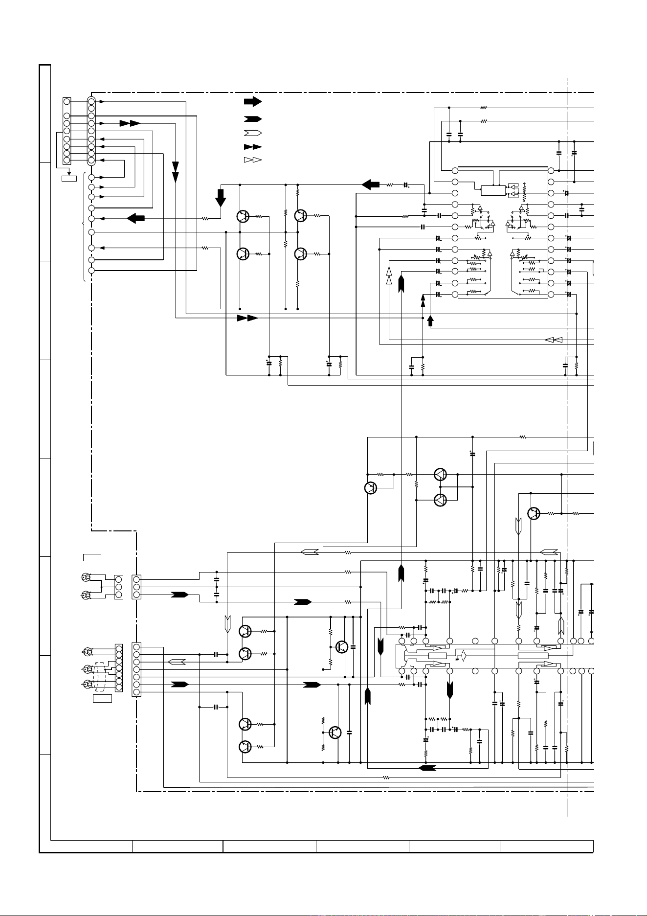
Figure 18 SCHEMATIC DIAGRAM (1/10)
A
B
C
D
E
F
G
H
1
23456
• NOTES ON SCHEMATIC DIAGRAM can be found on page 14.
0.7V
0V
0V
0V
0.7V
0V
0V
0V
0V
0V
0V
0V
3.4V
3.4V
0V
0V
9.3V
8.6V
9.3V
0V
0.7V
0.7
V
0V
0V
0V
0.7V
0.7V
24
23
22
21
20
19
18
17
16
15
14
13
12
11
10
9
8
7
6
5
4
3
2
1
17 16 15 14 13
89
10 11 12
1819
20
56 7
23 22 21
23 4
24
1
REC_R
+B
T2_R2
L
R
A_GND
L
L
R
R
TO POWER SECTION
P22 1-F
CD_+B
CD_GND
L-CH
A_GND
R-CH
CNP5
TO
CD SERVO
PWB
P27 12-D
T1_R
T1_L
A_GND
M_GND
ERASE
T2_R1
T2_L1
T2_L2
ERASE HEAD
RECORD/
PLAYBACK HEAD
TAPE 2
TAPE 1
PLAYBACK HEAD
R-CHL-CH
R-CH
L-CH
3
6
3
2
1
4
3
2
6
1
5
7
8
D_GND
LD+7V
LD+7V
A_5V
D+5V
CD_GND
L-CH
A_GND
R-CH
CD_A_GND
CD_D_GND
4
5
7
3
1
2
6
9
10
11
12
13
14
15
16
17
18
8
7
5
2
4
1
5
1
2
6
3
4
7
3
1
2
–
+
–
+
–
+
–
+
–
+
–
+
–
+
–
+
CCB
INTERFACE
AUX
DECK
TUNER
CD
112K
56K
112K
56K
Hich=CHROME
–
–
+
+
Hich=T1
+
–
+
–
Nor/CrO2
RIPPLE
ALC
ALC
Vcc
LSEL0
R1
R2
R3
R4
RSEL0
RIN
RTRE
RBASS
ROUT
VREF
VDD
CLK
L1
L2
L3
L4
LIN
LTRE
LBASS
LOUT
VSS
CE
DI
1
1
2
23
3
+B
+B
+B
IC101
AN7345K
FM SIGNAL
PLAYBACK SIGNAL
RECORD SIGNAL
CD SIGNAL
VIDEO SIGNAL
SWITCHING
SWITCHING
MUTING
M
U
SWITCHING
SWITCHING
SWITCHING
SWITCHING
SWITCHING
BI601
CNS601
R619
330
R618
330
Q603
KTC3199 GR
R617
2.2K
R616
2.2K
R615
3.3K
R614
3.3K
Q604
KTC3199 GR
Q601
KTC3199 GR
R613
390
R611
2.2K
R610
2.2K
Q602
KTC3199 GR
R612
390
R605
10K
C609
1/50
R607
3.9K
C607
0.15
C605
0.12
C611
0.0022
C613 1/50
C615 4.7/50
C617 1/50
C619 1/50
C621
1/50
IC601
LC75341
AUDIO PROCESSOR
C651
220P
C652
220P
R602
1K
R601
1K
C653
220P
C601
220/16
C603
22/50
C608
0.15
C606
0.12
C624
1/50
C622 1/50
C620 1/50
C618 1/50
C616 4.7/50
C614 1/50
C626
0.0022
R608
1.2K
C625
0.0022
R609
1.2K
R620
22K
C640
22/50
R621
22K
C639
1/50
CNP101
CNP102
Q103
KTC3200 GR
Q101
KTC3200 GR
R105
3.3K
R103
2.2K
C105
560P
Q105
KTC3199 GR
R109
4.7K
R107
47K
R108
47K
R110
4.7K
C106 560P
Q106
KTC3199 GR
R112
15K
R101
1K
R102
1K
R114
1K
C110
330P
C108
330P
R120
3.9K
R118
100K
C114
0.033
R124
5.6K
C118
47/25
C116
560P
C112
47/25
R122
12K
C120
0.0022
R116
56
C150
47/50
R150
68K
R126
4.7K
Q113
KRC104 M
Q114
KRC104 M
R146
10K
R147
10K
R148
4.7K
Q112
KTA1266 GR
C141
100/16
R149
150
R136
220K
R138
10K
R139
10K
Q108
KTC3199 GR
Q1
KTC31
IC101
AN7345K
PLAYBACK
AND
RECORD/
PLAYBACK
AMP.
C128
0.022
C124 270P
C132
47/25
C130
0.0033
R132
100
R130 1.5K
R134
10K
C133 22/50
C134 220/10
R128
5.6K
C126
22/50
C107
330P
R113
1K
C109
330P
C125
22/50
C131
47/25
C121
0.022
R129
5.6K
C143
3.3/50
R131 1.5K
R127
4.7K
R133
100
C127 0.022
C129 0.0033
C123
270P
R135
10K
R119
3.9K
R117
100K
R123
5.6K
C113
0.033
C115
560P
C117
47/25
R115
56
C111
47/25
R121
12K
C119
0.0022
R111
15K
Q104
KTC3200 GR
Q102
KTC3200 GR
R104
2.2K
R106
3.3K
C104
180P
C101
560P
C102
560P
C103
180P
C623
1/50
Q603, Q604: SYSTEM MUTE
– 19 –
CD-E700H
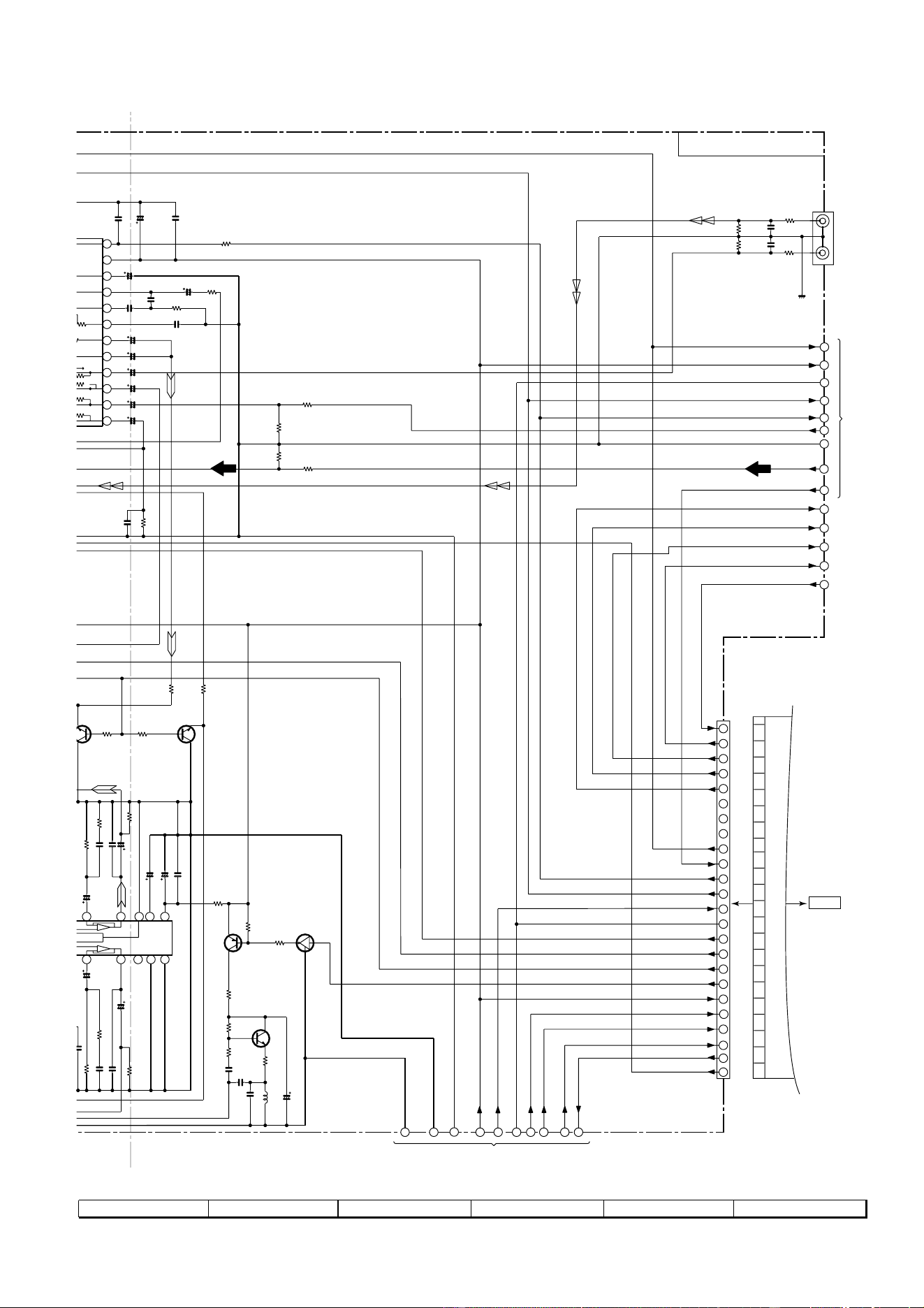
Figure 19 SCHEMATIC DIAGRAM (2/10)
7
8 9 10 11 12
0.7V
0.7V
0V
0V
0V
0V
0V
11.6V
11.6V
0V
0V
19 20 21 22 23 24 25 26 27 28
1
2
3
4
5
6
7
8
9
29
30
31
32
33
24
23
22
21
20
19
18
17
16
15
14
13
17 16 15 14 13
89
10 11 12
A+10V
+B_PROTECT
M_+13V
SP_RLY
SW_5V
SP_DET
TAPE_A_GND
AGND
REC_R
A+10V+B
+B
+B
+B
+B
+B
+B
+B
+B
+B
REC_L
(AUDIO PRO)
D_GND
M_GND
SW_5V
S_MUTE
M_+13V
TO MAIN PWB
P21 9-G
+B_PROTECT
–20dB
SP_DET
D_GND
SP_RLY
REC/PLAY
T_T1/T2
T_BIAS
CLK
DI
CE
FFC701
CNP701A
TO
DISPLAY PWB
P24 1-F
DO
11
16
15
14
13
12
10
9
8
7
20
24
24
23
22
21
19
18
17
6
5
4
3
2
1
1
A+10V
DGND
DI
CLK
AGND
TUN_L
RDS-READY
RDS-READY
RDS-RDCL
RDS-RDCL
RDS-RDDA
RDS-RDDA
RDS-RST
RDS-RST
TUN_SM
TUN_SM
DO
TUN_R
CE
CHASSIS
R-CH
L-CH
MAIN PWB-A1(1/3)
TO POWER SECTION
P22 1-F
56K
56K
C
HROME
–
–
+
+
Nor/CrO2
RIPPLE
ALC
ALC
Vcc
R1
R2
R3
R4
RSEL0
RIN
RTRE
RBASS
ROUT
VREF
VDD
CLK
1
23
MUTING
MUTING
SWITCHING
BIAS
BIAS OSC.
O
R
C653
220P
C601
220/16
C602
0.022
R603
1K
C603
22/50
C608
0.15
C610
1/50
R604
10K
C612
0.0022
R606
3.9K
C606
0.12
C624
1/50
C622 1/50
C620 1/50
C618 1/50
C616 4.7/50
C614 1/50
R642
10K
R643
22K
R641
10K
R644
22K
C626
0.0022
R608
1.2K
R137
220K
R136
220K
R138
10K
R139
10K
Q108
KTC3199 GR
Q107
KTC3199 GR
C128
0.022
C132
47/25
C130
0.0033
R132
100
R130 1.5K
R134
10K
C133 22/50
C134 220/10
C135 0.022
C126
22/50
C125
22/50
C131
47/25
R131 1.5K
R133
100
C127 0.022
C129 0.0033
R135
10K
C138
0.0082
C137
0.047
(ML)
C140
47/25
Q111
KTC3203 Y
R142
82 (1/2W)
C139
0.039(ML)
R143
47K
L103
330 µH
R144
22K
R145
4.7
Q110
KRC104 M
R141
4.7K
R140
47K
Q109
KTA1266 GR
R158
220
CNP701B
R690
6.8K
C690
390P
R691
6.8K
C691
390P
R693
33K
R692
33K
JK690
VIDEO/AUX IN
CD-E700H
– 20 –
A
B
C
D
E
F
G
H
1
23456
• NOTES ON SCHEMATIC DIAGRAM can be found on page 14.
Figure 20 SCHEMATIC DIAGRAM (3/10)
+B
+B
+B
+B
FM IF
FM SIGNAL
AM SIGNAL
AM BAND
COVERAGE fL
T306
AM OSC.
T303
AM ANTENNA
AM TRACKING
T351
AM IF
47P
0.001
270
330P
47K
68K
2.7K
0.001
15P
0.022
470
0.022
0.022
150
SVC348S
3.3/50
0.022
6.8K
330
33
0.01
1K
DS1SS133
DS1SS133
0.001
2.2/50
100/10
1/50
1K
15
2.2µH
0.022
15P
0.047
0.022
6
43
2
1
0.022
4.7K
0.022
0.022
10K
1K
1K
100/16
2SC380 O
OSC.BUFFER
0.022
2.2/50
1K
22K
0.001
10K
0.001
0.022
1K
1K
1.5K
1/50
0.022
2.2K
10/50
0.01
100µH
560P
22P
47K
4.7K
1/50
0.022
0.022
3.9K
0.022
5.6K
10K
12P
33
680
0.022
0.022
10/50
47/25
8
7
6
5
43 2 1
1234567891011
1213141516171819202122
123
4
5
6
7
8
91
0
161718192021222324
4.5 MHz
TP301
TP302
CONT
IF
FM/AM
FM/AM
(UJ)
(SL)
(CH)
SD
TP
(CH)
(CH)
ST IND
MO/ST
FM FRONTEND
F OUT
IF OUT
VCC
VT
GND
GND
GND
ANT
VSS
AOUT
AIN
PD
VDD
FM IN
AM IN
DO
CL
DI
CE
X IN
X OUT
IF IN
REG
AM IF IN
GND
SD
STEREO
FM DET
VCC
IF OUT
MPX IN
MPX VCO
FM/AM OUT
VSM
AM LOW CUT
AM RF IN
AM OSC IN
FM AFC
AM OSC OUT
AM MIX OUT
FM IF IN
2
1
1
3
2
SO301
FM
ANTENNA
TERMINAL
AM LOOP
ANTENNA
1
2
C302
C338
C323
D302
D301
CNP302
L341
BALUN
R323
VD301
C335
C334
C330
C332
R336
CF302
R345
C346
C321
C345
R344
C347
CF301
R347
R346
R399
C348
Q301
R348
R349
L342
R369
C341
FE301
R378
R372
R374
R373
C383
C382
X352
C397
R382
R381
C392
R380
C393
C380
C381
C394
C386
C387
R379
C385
L351
R377
R395
R376
R360
R386
IC302
LC72131
PLL(TUNER)
C398
R393
C351
C350
C352
CF352
R353
C399
R352
C354
CF351
C357
C389
C362
C361
R365
C342
R358
R351
C366
C363
C364
C365
R357
X351
456 kHz
L354
LOW PASS FILTER
C368
R356
R350
C367
C369
C331
C353
1
1
2
3
2
3
– 21 –
CD-E700H
Figure 21 SCHEMATIC DIAGRAM (4/10)
7
8 9 10 11 12
29303132338
6
3729541
+B
+B
+B
+B
+B
MAIN PWB-A1 (2/3)
0.022
390
1K
0.001
DZ5.1BSB
0.001
47/25
10K
1K
1K
1K
1K
2.2µH
47/25
0.022
LC72723
9
10
11
12
13
14
15
16
8
7
6
5
4
3
2
1
0.022
2.2µH
47/25
47/25
0.022
560P
56K
56K
10K
0.022
KTC3199 GR
4.332 MHz
22P
390
6.8K
10K
270
0
P
47K
5.6K
47/25
5.6K
470K
0.015
0.022
1/50
2.2/50
0.001
100/10
1/50
1K
22P
270
5.6K
KTA1266 GR
SWITCHING
270
0.022
100/10
DZ5.1BSB
0.015
27P
1.8K
3.3K
K
1K
1/50
5.6K
22K
3.9K
100µH
1/50
1/50
47K
4.7K
0
.
022
7
8
91011 12
1314151617
22P
TUN_R
TUN_L
TUN_SM
RDS_RST
RDS_RDDA
RDS_RDCL
RDS_READY
AGND
DGND
A+10V
DO
CLK
DI
CE
(CH)
(UJ)
XOUT
TEST
CIN
FLOUT
VSSA
VDDA
MPXIN
XIN
READY
RDS-ID/
RDCL
RDDA
RST
MODE
VDDD
VSSd
VREF
TP302
TP
MO/ST
STEREO
FM DET
VCC
IF OUT
PHASE
(FM/AM)
PHASE
L-CH OUT
R-CH OUT
MPX IN
MPX VCO
(CH)
86
R395
76
R360
TO MAIN PWB
P19 12-C
R386
C388
C384
R384
C391
R383
R385
Q360
R359
R392
R391
C395
C396
ZD351
L352
C398
R387
R388
R393
R353
C399
C354
CF351
C356
C358
C357
R355
C370
R357
X351
456 kHz
C373
L354
P
ASS FILTER
C368
R356
C374
C371
C372
C369
IC303
LA1832S
FM IF DET./FM MPX./AM IF
R370
CT22
RT23
ZDT21
CT21
RT21
RT30
RT29
RT28
RT27
LT21
CT24
LT22
RT22
CT30
CT27
CT32
CT31
CT28
CT26
QT21
ICT21
XT21
RT32
RT31
CT23
RT26
CT29
RT24
RT25
CT25
C355
ICT21
LC72723
RDS DECORDER
CD-E700H
– 22 –
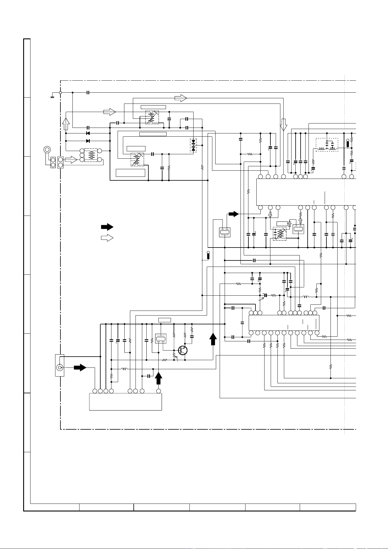
Figure 22 SCHEMATIC DIAGRAM (5/10)
A
B
C
D
E
F
G
H
1
23456
• NOTES ON SCHEMATIC DIAGRAM can be found on page 14.
13V
-B
-B
-B
-B
-B
-B
-B
-B
-B -B
+B
+B
+
B
+B
+B
+B
+B
+B
+B
+B
+B
+B
+B
-B
R912
100(1/4W)
Fusible
1
KTC3199 GR
DS1SS133
100/50
100/50
1.8K
1.5K
0.01
0.1(ML)
0.22
10
0.22
10
DS1SS133
0.1
DS1SS133
DS1SS133
0.1
3
1
10K
0.1
0.1
10/50
22K
220
DZ8.2BSB
22/50
DS1SS133
DS1SS133
3
1
3
1
47K
47K
3300/71
1N4004S
12BSB
33K
DS1SS133
47/50
56K
56K
0.1
39K
39K
DS1SS133
1N4004S
STK41242
KTC3199 GR
4700/35
DS1SS133
KTC3199 GR
56K
3.3P(CH)
1K
56K
3300/71
4700/35
12BSB
0.1/50
100/100
1.5K
1.5K
22/50
560
100P
560
1.5K
0.001
0.001
56K
100/100
1K
22/50
56K
0.01
KTC3199 GR
0.1
1.8K
0.22
1K
100/100
0.1/50
1K
0.1/50
56K
0.22
100P
3.3P(CH)
100/100
22K
0.1
22K
0.1
321456710 9 813 12 1116 15 1418 17
3300/35
2
2
2
D+5V
LD+7V
A+10V
M_+13V +B
+B
+B
+B
+B
+B
+B_PROTECT
A_5V
SW_5V
TAPE_A_GND
CD_A_GND
CD_D_GND
D_GND
M_GND
A_GND(AUDIO PRO)
CD_GND
(3W)
(3W)
(ML)
(1/2W)
(1/2W)
(ML)
(ML)
(ML)
(ML)
(ML)
CHASSIS
(1/2W)
L
R
AC_RLY
VF1
P_IN
–VF
VL+
V
H
V
H
(ML)
(ML)
VH+
VH– VL–
VL+
(3W)
SP_DET
POWER AMP.
(3W)
TO MAIN PWB P18 1-B, P19 10-H
1
4
3
2
5
6
VF2
VL–
1
3
2
4
5
6
7
8
9
10
3
2
4
5
6
7
8
9
10
1
3
2
4
5
6
7
8
9
10
11
1
CHASSIS
L_CH
A_GND
R-CH
SP_DET
SP_RLY
GND
VL+
VL–
VH–
VH+
–
+
–
+
14
15
16
27
28
25
10
22
23
12
11
26
13
21
19
24
17
18
20
FROM
DISPLAY PWB
P25 12-E
FW701
MAIN PWB-A1 (3/3)
FM SIGNAL
R958
100(1/4W)Fusible
C909
R909
C908
R907
C905
R905
C913
R906
R918
C912
R910
C906
R911
R919
R913
R903
R904
R916
C907
C910
C914
C918
C916
ZD903
IC901
D906
Q902
ZD902
R926
R925
C917
R917
C927
R934
L902
3µH
D907
Q904
Q903
C929
R941
R939
R930
C923
D910
C925
R935
L901
3µ H
R937
R929
R928
R927
D909
C922
C920
C921
Q901
D905
R920
R921
C919
R922
R908
C915
R902
C904
C903
C911
R901
C902
C901
C946
R860
D858
CNP801
BI801
CNS801
D855
C855
C864
D859
R854
C851
R853
C854
C856
D857
D852
ZD852
D851
C865
R859
C863
R961
C858
R852
C859
R801
CNP802
C861
IC851
KIA7812AP
IC851
KIA7812AP
VOLTAGE
REGULATOR
IC855
KTC2026
SILICON
IC853
KIA7805AP
VOLTAGE REGULATOR
IC852
KIA7810AP
VOLTAGE REGULATOR
IC853
KIA7805AP
– 23 –
CD-E700H
Figure 23 SCHEMATIC DIAGRAM (6/10)
7
8 9 10 11 12
5.6V
1
2
1
2
PT841
SUB POWER
TRANSFORMER
-B
-B
+B
+B
+B
+B
+B
+B
+B
-B
When Servicing, pay attention as the area
enclosed by this line ( ) is directly
connected with AC main voltage.
TRANSFORMER
PWB-B2
POWER PWB-B1
DZ6.2BSA
100P
2.2µH
100P
47K
KTC3199 GR
1.5K
1.5K
68K
10/50
15K
DS1SS133
390
DS1SS133
1K
390
KTC3203 Y
FAN MOTOR
DRIVER
0.001
0.001
0.022
0.022
0.022
0.022
6.8
6.8
0.022
0.022
6.8
6.8
0.022
0.022
82
0.1
1N4004S
0.1
1N4004S
470/35
0.22
10
0.22
10
47K
100K
220
D10XB60F
1000/6.3
KTC3199 GR
47K
1K
31
220K
1N4004S
1N4004S
1N4004S
1N4004S
0.022
10
56K
56K
10
0.22
0.22
56K
D10XB60F
0.1
0.1
220/63
2.2K
KTA1274 Y
12K
100/35
47K
DZ6.2BSA
47/50
47/50
DZ30BSB
1N4004S
1N404S
22/100
DS1SS133
2
(1/2W)
T4A L 250V
T4A L 250V
T2A L 250V
T2A L 250V
M901
FAN
MOTOR
CHASSIS
(1/2W)
(1/2W)
L
R
AC_RLY
VF1
P_IN
–VF
R
L
L
L-CH
GND
R-CH
SP_RLY
M_+13.5V
UNSW_
SP_L1-CH
SP_R1-CH
SP_L1-CH_GND
SP_R1-CH_GND
–
+
VL+
VH–
VH+
6 OHMS MIN
4.4V
0.2V
(2W)
(1/2W)
(1/2W)
(2W)
R1_OUT
L1_OUT
(ML)
(ML)
(ML)
(ML)
1
M
47
47
1
4
3
2
5
6
VF2
VL–
1
3
2
4
5
6
7
8
9
10
3
2
4
5
6
7
8
9
10
1
3
2
4
5
6
7
8
9
10
11
1
4
4
1
1
AC POWER
SUPPLY CORD
AC 230 V, 50 Hz
CHASSIS
1
1
1
5
5
2
3
4
5
HEADPHONES
PWB-A3
1
2
2
FROM
DISPLAY PWB
P25 12-E
FW701
SO901
SPEAKER
TERMINAL
L
C927
R934
L902
3µH
RL914
Q905
R945
R944
D911
R942
R943
C931
R947
L702
WTM901
R950
D912
R949
MOTOR DRIVER
SP RELAY
ON-OFF
Q906
CNP705
CNP971
FW901
CNS971
C719
C718
L920
0.29µH
L921
0.29µH
R946
C934
C936
C938
C940
C939
C941
C937
C935
C929
R941
R939
R938
R940
C928
C926
R935
L901
3µ H
R937
D801
CNP801
BI801
D804
D802
C811
0.22
(ML)
C810
0.22
(ML)
C809
C808
F802
F801
CNP805
CNS805
F805
T2A L 250V
RL841
ZD802
C807
D803
C806
ZD803
D805
C805
F804
F803
R802
R803
C801
C803
CNS801
R844
R801
R841
R804
R805
C804
R808
Q801
R806
ZD801
C802
CNP802
C841
C843
0.047(ML)
D806
WTM801
FW802
T.F.
D846
C844
0.047
L841
LINE FILTER
C842
WTM802
Q841
R843
R842
D842
D843
D844
D845
D853
1N4004S
RELAY
DRIVER
VOLTAGE
REGULATOR
IC854
AN78L05
VOLTAGE
REGULATOR
D856
DS1SS133
C861
C942
C943
R952
R954
R953
R955
R858
PT801
MAIN POWER
TRANSFORMER
BR
BL
JK701
HEADPHONES
CD-E700H
– 24 –
A
B
C
D
E
F
G
H
1
23456
• NOTES ON SCHEMATIC DIAGRAM can be found on page 14.
Figure 24 SCHEMATIC DIAGRAM (7/10)
+10V
3
2
1
Q711
KRA107 M
D706
DS1SS133
2
1
3
LED B PWB-A5
LED A PWB-A4
80
79
78
77
76
75
74
73
72
71
70
69
68
67
66
65
64
63
62
61
60
59
58
57
56
55
54
53
52
51
4.7K
DS1SS133
DS1SS133
47/25
0.0047
0.0047
1K
330
A503BC2E
A503BC2E
330
10K
1K
DS1SS133
10K
10K
1K
1K
1K
1K
DS1SS133
1K
47K
1.5
1K
10K
10K
1K
1K
10K
1K
1K
10K
10K
10K
1/50
10K
KTA1273 Y
KTA1273 Y
KTA1273 Y
10K
10K
1K
680
680
2.2K
560
50 49 48 47 46 45 44 43 42 41
82 83 84 85 86 87 88 89 90 81
KRC102 M
A+10V
RDS-RST
RDS-RDDA
RDS-RDCL
RDS-READY
TUN SM
JOG B
JOG A
O/C_SW
S_MUTE
M_+13V
SW_5V
M_+13V
ILU_LED1
DIST0/S20
DIST1/S19
DIST2/S18
DIST3/S17
DIST
+B_PROTECT
S21
S11
S10
T1 RUN
MIC SW
ESS ACK
ESS STB
ESS DI
ESS DO
NP
NX
NX
NX
NX
NX
NX
NX
F
F
S2
S3
S4
S5
S12
S13
S14
SMUTE
T_SOL_A
T_MOTOR
TIMER LED
VDD
AC_RLY
P21
P20
P19
P18
P17
P16
P15
P14
P13
P12
P11
P10
P09
P08
P07
P06
P05
P04
P03
P02
T_SOL_B
SP_RLY
D_GND
T2 RUN
FPA/FPB
REC/PLAY
T_T1/T2
T_BIAS
DI
CE
CLK
DO
SP_DET
–20dB
S6
S7
S8
S9
VLOAD
S15
S16
SP_RLY
11
2
1
11
23
21
15
7
45 44 43 42 41 40 39 38 37 36 35 34 33 32 31 30 29 28 27 26 25 24 23 22 21 20 19 18 17 16 15
1
2
3
4
5
6
8
9
10
11
12
13
14
16
20
18
19
17
24
2
1
22
2
2
2
2
T2 RUN
+MTR
SOL2
SOL1
T1 RUN
GND
F_REC
7
5
6
4
3
2
1
TAPE MECHANISM
PWB-F
SOL
SOL
+
–
M
7
7
6
1
2
1
4
3
5
FFC702
TO
MAIN PWB
P19 12-F
CNP701B
FFC701
+B
+B
+B
+B
+B
+B
+B
+B
+B
+B
+B
+B
+B +B
+B
BI703
BI704
LED703
LED704
CNS703
CNS704
CNP703
CNP704
R751
LED DRIVER
R749
Q710
R794
C707
FL701
FL DISPLAY
R730
R725
R726
R727
R728
R729
R764
R758
R731
R762
R732
R735
R746
R734
R757
R742
R743
R744
R745
IC70
1
IX0553
A
SYST
E
MICROCO
M
R788
R789
R770
R772
CNP701A
CNP702
R740
D710
D709
C712
Q708
Q706
Q707
R779
R777
R778
C709
JOG701
VOLUME JOG
C710
R776
R775
R780
D704
D701
R750
2
1
3
Q712
KRC104 M
MOTOR
DRIVER
SOLENOID
DRIVER
SOLENOID
DRIVER
– 25 –
CD-E700H
Figure 25 SCHEMATIC DIAGRAM (8/10)
7
8 9 10 11 12
2
1
3
30
29
28
27
26
25
24
23
22
21
20
19
18
17
16
15
14
13
12
11
10
9
8
7
6
5
4
3
2
1
0.0047
100µH
1K
1K
1K
1K
10K
1K
1K
DS1SS133
1.5
10K
1K
0.022
10K 3.9K 5.6K
1K680 820
100
2.2K 2.7K
4.7K
1K
0.022
10K
10K
10K
10K
DS1SS133
3.3/50
47/25
DS1SS133
DS1SS133
47K
100
KRC102 M
100K
DS1SS133
0.01
4.7K
10K
4.7K
10K
304VT2E
10K
1K
5.6K
1K
1K
1K 1.5K
1K820
820 680
1.5K 3.9K2.2K 2.7K680
4.7K
10K
1/50
15P
1K
1K
1K
1K
1K
1K
100
1K
1K
1K
1K
1K
1K
680
680
2.2K
560
1K
1K
1K
220/10
18P
1K
1 2 3
4
9 48 47 46 45 44 43 42 41
40
31 32 33 34 35 36 37 38 39
93 94 95 96 97 98 99
100
8
2 83 84 85 86 87 88 89 90 91 92
DISC_NO SW/
ASPM
DISPLAY
MODE
PTY TI
SEARCH
VIDEO/
SKIP
DISC
JOG
A
O/C_SW
S
W
DRF
VF2
–VF
VF1
P_IN
UNSW5.6
CD CLK
L
ED1
0
/S20
1
/S19
2
/S18
3
/S17
T2_PLAY SW/
LVL_DET
CLOCK
DOWN
TUNING
UP
KEY 0
KEY 1
KEY 2
S10
CD CLAMP SW
FPA/FPB SW
PROTECT
U
N
S
W
A
CK
S
TB
DI
DO
NX
NX
NX
NX
NP
5V BACK UP
T-BIAS
T_T1/T2
VDD
X1
X2
AVDD
RESET
CD CE
CD DI
S1
S2
S3
S4
S5
CE
REC/PLAY
CD RESOUT
VPP/IC
CD DO
CLK
DI
DO
AVSS
TUN SM
KEY 2
KEY 1
KEY 0
P_IN
REMOCON
VSS
SMUTE
T_SOL_A
T_MOTOR
TIMER LED
VDD
AC_RLY
G9
G8
G7
G6
G5
G4
G3
G2
G1
VDD
P06
P05
P04
P03
P02
P01
G01
G02
G03
G04
G05
G06
G07
G08
G09
F
T_SOL_B
ON/
STAND-BY
EQUALIZER
CD
TUNING
DISC_NO SW
WRQ(DSP)
CLAMP SW
CD DO
CD DI
CD CE
CD CLK
U
N
–20dBATT
XT2
AVREF
DRF
RES OUT
X-BASS/
CLOSE
OPEN/
DEMO
TUNER
S6
S7
S8
S9
A
D
SP_RLY
SP DET
WRQ
AUX
MEMORY
SET
TAPE STOP PLAY
FAST
FORWARD
FAST
REWIND
TIMER/
SLEEP
REC./
PAUSE
DSA DATA
2
322212019181716151413121110 9 8 7 6 5 4 3 2 1
AC_RLY
2
3
1
4
5
6
7
8
9
11
10
1
2
3
4
5
6
7
8
9
10
TO
POWER PWB
P23 7-G
CNP802
FW701
+B
+B
+B
+B
+B
+B
+B
+B
+B
+B
+B
+B
A
Y
R795
C701
C702
R706
R763
R702
R703
R705
R704
C704
XL701
4.194304 MHz
R708
C705
C721
R711
R709
R710
R712
R739
R737
R713
R714
R715
R716
R717
R769
R791
C720
R722
R747
R759
R718
R719
R720
R730
R725
R736
R733
R721
R724
R726
R727
R728
R729
R731
R762
IC701
IX0553AW
SYSTEM
MICROCOMPUTER
JOG701
V
OLUME JOG
C710
R776
R775
R780
R765
R761
R756
LED701
R768
R773
R766
R767
SW710SW709SW708SW707SW706SW704 SW705SW703SW702SW701
RD09RD07 RD08RD05 RD06RD03 RD04RD02RD01
SW717SW711 SW712 SW713 SW718SW714 SW715 SW716
RD12RD11 RD13 RD16RD14 RD15RD10
SW723SW721
SW722
SW724
RD21RD19 RD20
L701
R781
C715
D713
D714
C714
RX701
C717
R783
Q709
R782
D715
D712
D711
WTM701
BI701
CNS701
CNP6
TO
CD SERVO PWB
P27 12-B
DISPLAY PWB-A2

CD-E700H
– 26 –
A
B
C
D
E
F
G
H
1
23456
• NOTES ON SCHEMATIC DIAGRAM can be found on page 14.
Figure 26 SCHEMATIC DIAGRAM (9/10)
CD MOTOR PWB-D
1
2
4
1
6
5
20
19
18
17
16
15
14
13
12
11
10
9
8
7
6
5
4
3
2
1
80 79 78 77 76 75 7
4
2
7
21 22 23 24 25 26
15 16 17 18 19 20 21 29 22 23 24 25 26 27 28
14
1 2 3 4 5 6 7
30
8
9
10 11 12 13
(OS)
VCC
VREF
VIN4
GND
VCONT
VIN2
VIN3
REG-OUT
REG-IN
VIN1
VCC1
VO+
VO–
VO2–
VO2+
VO3+
VO3–
VO4–
VO4+
VCC2
VO5+
FWD
REV
VO5–
GNDGND
TP2
TP1
M–
M+
SPO
VCC
VREF
TO
FD
C
F
B
A
E
VREF
VCC
CD SERVO PWB-C
LDD
LDS
FR
VVDD
PCKIST
VVSS
PDO2
CONT5
CONT4
GPDAC
SLDO
SPDO
FDO
CONSTANT
VOLTAGE
TDO
REF1
VREF
ADAVSS
ADAVDD
JITTC
RFMON
TE
TEC
FE
TIN2 F
TIN1 E
FIN2 B
FIN1 A
RSVSS
RFVDD
RF
EFMIN
LASER DRIVER
SLCIST
SLCO
GND
FO–
LD
VR
PD
FO+
TR+
TR–
6
3
7
1
2
5
8
4
6
3
7
1
2
5
8
4
GND
PUIN
SL+
SL–
SP–
SP+
HPC1LX
PICKUP UNIT
GND
TR–
TR–
TR+
TR+
FO+
FO+
FO–
4
8
5
2
1
7
3
6
5
3
6
2
7
1
4
5
3
6
2
7
1
4
5
3
6
2
7
1
4
VREF
VCC
E
A
B
F
C
PD
LD
+
+
–
–
M
M
6
5
4
3
2
1
6
5
4
3
2
1
6
5
4
3
2
1
VR
+B
+B
+B
+B
+B
+B
+B
CD SIGNAL
5
3
6
2
7
1
4
2
5
4
8
3
6
7
1
6
5
4
3
2
1
CNP1
CNS1A
CNS1B
CNS2A
CNS2B
CNS3A
CNS3B
CNP3A
R6 22K
R5 8.2K
R4 8.2K
R3 22K
R1
8.2K
R2
8.2K
C2
0.01
C1
47/25
R9
10
Q1
KTA1266 GR
C3
47/25
C4
0.001
R7
47
C8
0.0027
R11
10K
C5
0.047(ML)
C6
0.1
C19
0.022
R10
27K
R12
330
C45
22P(CH)
C20
0.001
C21
0.001
C43
0.022
C9
3.3/16
C11
0.22/50
C10
10/25
C12
100P
R15
1K
R14
1K
R1
1
K
R16
1K
R13
15K
C39
100/10
C40
100/10
Q4
KTA1271 Y
L
C
IC2
LA6574H
FOCUS/TRACKING/SPIN/
SLED DRIVER
C48
0.001
C41
100/10
CNP3
CNP2
C38
0.01
C17
100/10
R8
10K
C2
C2
C3
C3
C
2
C36
0 22/50
R41
12K
R40
680
C37
0.1
R42
1.2K
M1
SPINDLE
MOTOR
M2
SLED
MOTOR
SW4
PICKUP IN
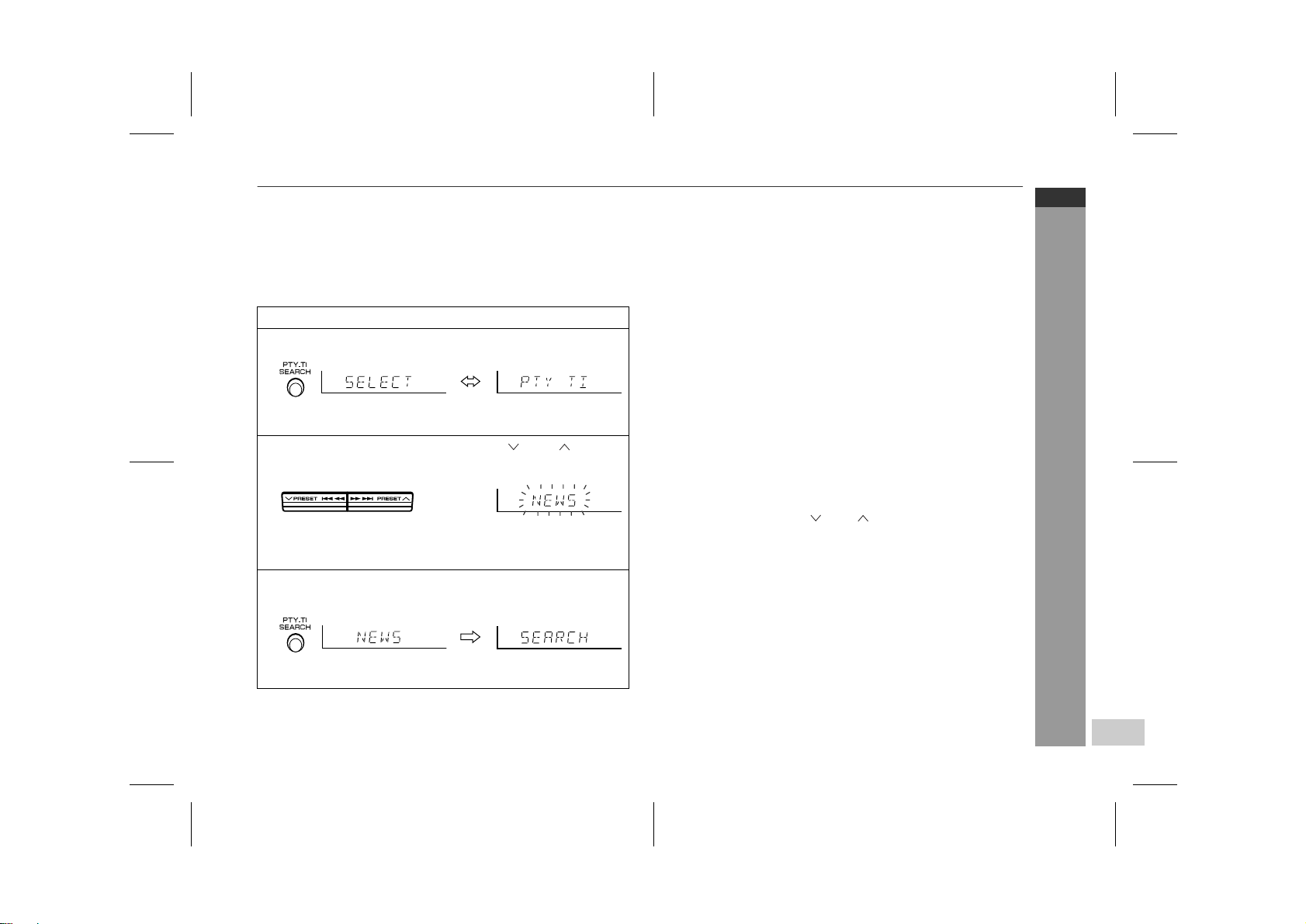
– 27 –
CD-E700H
Figure 27 SCHEMATIC DIAGRAM (10/10)
7
8 9 10 11 12
• The numbers 1 to 12 are waveform numbers shown in page 36.
CD LOADING
MOTOR PWB-E
1
6
9
10
3
78
11
12
5
60
59
58
57
56
55
54
53
52
51
50
49
48
47
46
45
44
43
42
41
20
19
18
17
16
15
14
13
12
11
10
9
8
7
6
5
4
3
2
1
80 79 78 77 76 75 74 73 72 71 70 69 68 67 66 61 62 63 64 65
27 28 29 30 31 32 33 34 35 36 37 38 39 40 21 22 23 24 25 26
D_GND
CONT1
DISC NO
CD RES
O/C,
A5V
LDD
LDS
FR
VVDD
PCKIST
VVSS
PDO2
PDO1
CONT2
CONT3
VSS
VDD5
DRF
∗RES
∗WRQ
DO
DI
CL
CE
DATA
BCK
LRCK
ASDFIN
ASDACK
ASLRCK
IGMOUT
EFLG
C2F
XVSS
FSX/16MIN
XIN
XOUT
XVDD
RVDD
RCHO
RVSS
LVSS
LCHO
LVDD
TEST
DOUT
VDD
VSS
MON15
MON14
MON13
MON12
MON11
FSEQ
V/∗P
DEFECT
SBCK/FG
CONT5
CONT4
GPDAC
SLDO
SPDO
FDO
TDO
REF1
VREF
ADAVSS
ADAVDD
JITTC
RFMON
TE
TEC
FE
TIN2 F
TIN1 E
FIN2 B
FIN1 A
RSVSS
RFVDD
RF
EFMIN
SLCIST
SLCO
CLAMP SW
CNS701
FROM
DISPLAY PWB
P25 12-D
CNS601
FROM
MAIN PWB
P18 1-B
CL
DI
DO
CE
DRF
WRQ
D5V
DGND
L-CH
AGND
R-CH
10
3
4
2
1
5
6
1
–
+
M
+6.5V
+B
+B
+B
+B
+B
+B
+B
+B
+B
+B
+B
+B
3
4
2
1
5
6
3
4
2
5
6
6
5
4
3
2
1
7
8
5
4
2
6
7
8
9
1
3
R15
1K
1
4
K
R18
1K
R16
1K
R
13
5K
R43
220
XL1
16.933 MHz
R22
100
R27
10K
C14
100/10
C23
10/25
L1
0.82 µH
C44
0.001
C26
0.0015
(ML)
R25
2.2K
C24
10/25
C25
0.0015
(ML)
R26
10K
C16
330/6.3
ZD1
DZ3.3BSB
C22
0.01
R24
2.2K
C13
0.022
R20
10K
R19
15K
IC1
LC78646E
CD SERVO
FOCUS/TRACKING/SPIN/
SLED DRIVER
C15
0.001
R46 1
R21 1
R8
10K
CNS4
BI4
C42
0.01
CNP5
CNP6
R32 1K
R33 1K
R38 1K
R34 1K
R36 1K
R35 1K
R37 1K
R31
4.7K
C28 100P
C29 100P
C33 100P
C30 100P
C27 0.022
C36
0.22/50
C35
0.047
(ML)
R41
12K
R40
680
C37
0.1
R42
1.2K
R39
680
R29 2.2K
R28 2.2K
CNP4
SW1
OPEN/CLOSE
SW2
CLAMP
SW3
DISC NUMBER
M3
T/T UP DOWN
LOADING MOTOR
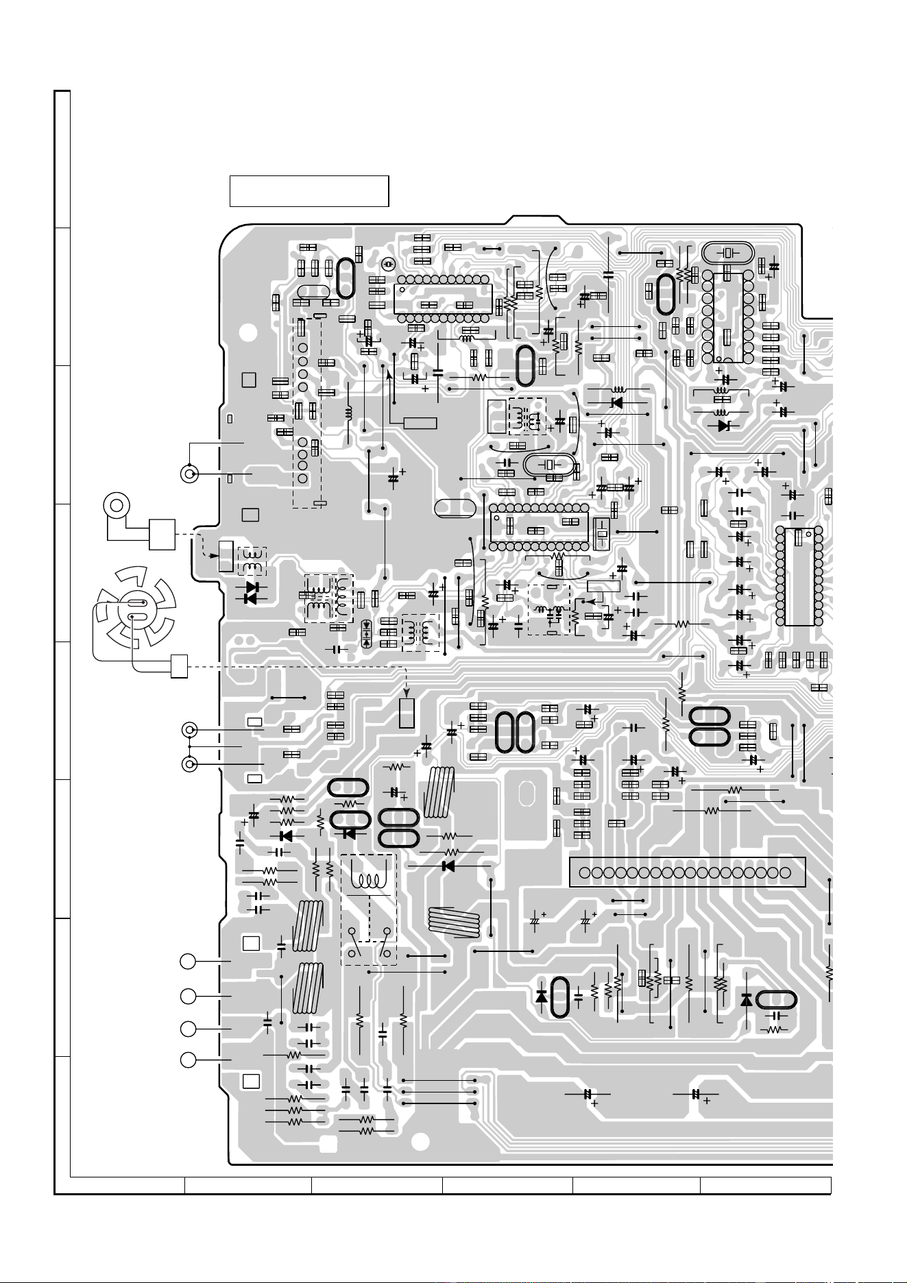
CD-E700H
– 28 –
Figure 28 WIRING SIDE OF P.W.BOARD (1/7)
A
B
C
D
E
F
G
H
1
23456
R910
R904
R902
R620
R605
R617
R616
R641
C625
R609
R608
C626
C612
R644
R606
C388
C653
RT21
RT32
CT27
CT28
RT30
CT29
RT29
RT25
RT28
CT26
CT30
RT27
RT31
RT26
CT25
CT23
CT22
RT24
R374
R378
R373
R372
R388
R359
R376
C395
R360
C387
R379
C386
C392
R377
R385
R395
R393
C385
R383
C351
C356
C350
C354
R353
R355
C353
R352
C355
C399
C366
R351
R365
C369
R350
C361
R356
C342
C363
R619
R613
R612
R615
R621
R614
R611
R610
R906
R905
C904
R901
C913
C903
R903
C907
R909
C908
R907
R908
C910
R693
C691
R692
R691
C690
R690
C335
C332
C338
C330
R323
R336
C334
C323
C347
R369
R345
C346
C345
R380
C341
R381
C397
R346
R348
R344
C381
C382
R347
R349
R399
C384
C348
C923
C921
R919
C917
D906
Q902
R918
R916
R917
R913
R911
R927
IC901
R912
R958
C85
1
C902
C640
R85
4
Q603
R618
Q604
R604
C624
C622
R642
C620
C618
IC601
C616
C614
C
C602
C606
C601
C608
C610
C603
ZDT21
LT22
CT31
LT21
CT24
CT32
ICT21
QT21
RT23
RT22
CT21
XT21
C383
IC302
R386
C396
R384
R387
L351
C391
C380
R392
R391
C393
Q360
R382
C389
L352
ZD351
T351
CF352
C398
C370
C352
CF351
C358
C357
CF302
IC303
X351
R370
C371
C367
C373
C362
R358
C374
C368
R357
C365
C364
C372
T306
C639
C909
Q601
Q602
C901
C946
C906
C905
L902
R934
R935
D907
L901
C911
C912
R922
R921
R920
C919
Q901
D905
C920
R938
R941
R940
R939
R953
C928
C927
C929
C937
C935
R955
C941
C926
C943
R942
R943
C939
L921
C942
L920
RL914
C938
C940
R954
R945
R944
R952
C934
C936
Q904
D912
D911
R947
C931
R950
Q905
Q903
R949
R946
C925
Q906
R937
C331
T303
D302
D301
CNP302
C321
L342
FE301
C394
CF301
Q301
X352
123456789101112131415161718
123456789
10 11
1213141516171819202122
123456789
10 11 12
131415161718
19
20212223
24
1
2
3
4
5
6
7
8
B
C
E
9
10
11
12
13
14
15
16
1
2
3
4
5
6
7
8
9
10
11
12
15
14
13
18
17
16
21
20
19
24
23
22
SO901
SPEAKER
TERMINAL
+
+
–
–
R-CH
R-CH
L-CH
L-CH
2
1
CNP971
CNS971
M901
FAN MOTOR
JK690
VIDEO/AUX
R-CH
L-CH
RD
BR
1
2
VD301
3
2
1
B
123
C
E
CN
S
TP302
TP301
2
1
AM LOOP
ANTENNA
L341
2
1
SO301
FM ANTENNA
TERMINAL
5
6
7
8
1
2
3
4
E
C
B
321
L354
E C B
E C B
E
C
B
E
C
B
BCE
BCE
ECB
ECB
B
C
E
ECB
MAIN PWB-A1

– 29 –
CD-E700H
Figure 29 WIRING SIDE OF P.W.BOARD (2/7)
7
8 9 10 11 12
R140
R146
R143
R108
R107
R144
C104
R106
C106
R112
R104
C105
R103
R102
R105
R101
C108
C109
C110
C107
R120
C116
R118
R150
C124
R128
R126
C135
C129
R124
R130
R132
C120
C130
R122
R134
R135
R133
R139
R127
R131
R137
R129
C119
C123
C121
R121
R119
C115
R123
R117
C102
C101
R110
R109
R607
R148
R147
R961
R620
R605
R617
R616
R641
C625
R609
R608
C626
C612
R643
R644
C611
R606
C652
C651
C653
21
RT32
RT30
RT29
RT28
RT27
RT31
CT23
CT22
C856
LG3
C859
Q110
R142
Q109
Q112
R141
C139
C140
C138
L103
C141
Q111
R145
C137
R111
Q106
Q104
CNP102
C103
Q102
R114
Q101
Q103
R116
R115
C112
IC101
C114
C118
C150
C126
C133
C128
C127
C134
Q108
C132
R158
R138
R136
C131
C125
Q107
C143
C117
CNP701B
R601
R603
C113
C111
R602
R113
CNP101
Q105
C615
Q113
Q114
BI601
C613
R149
D852
D851
D857
R859
ZD852
C863
D859
R860
C865
C858
D858
R852
R853
C855
C854
IC853
IC852
IC851
C864
IC855
D910
R930
ZD903
C918
R928
R929
D855
R926
D909
R925
ZD902
C922
C921
R919
C917
D906
C916
Q902
R918
R916
R927
C914
C915
R958
C851
C640
R854
Q
604
C623
C624
C621
C622
C619
C620
C617
C618
IC601
C616
C605
C607
C614
C609
C602
C606
C601
C608
C610
C603
ZDT21
LT22
CT31
LT21
CT24
CT32
ICT21
CT21
XT21
1234567
8
1
2
3
4
5
6
7
8
9
10
11
12
13
14
15
16
1
2
3
4
5
6
7
8
9
10
11
12
15
14
13
18
17
16
21
20
19
24
23
22
1
2
3
4
5
6
7
8
9
10
11
12
15
14
13
18
17
16
21
20
19
24
23
22
1
1
3
5
7
9
2
4
6
8
11
13
15
17
19
21
23
10
12
14
16
18
20
22
24
9
1
1
2
3
4
5
6
7
23
CNS601
12345678
CNP5
TO CD SERVO PWB
P32 4-A
RD
BL
BL
BL
BL
GR
GR
GR
BL
RD
BL
BL
BL
GR
GR
GR
FFC701
124
CNP701A
TO DISPLAY PWB
P31 12-D
RD
FROM
TAPE1 PLAYBACK HEAD
P33 10-F
FROM
TAPE2 RECORD/PLAYBACK
HEAD
P33 11-F
BI801
CNS801
1
11
GR
WH
GR
WH
GR
WH
GR
GR
RD
WH
10
9
8
7
6
5
4
3
2
1
CNP801
TO POWER PWB
P34 4-A
FW901
WTM901
15
1
5
C719
C718
L702
CNP705
12345
JK701
HEADPHONES
HEADPHONES
PWB-A3
C B
C B
ECB
321321321
E
C
B
BCE
BCE
BCE
BCE
BCE
BCE
E
E
C
B
CB
E
C
B
E
C
B
E
C
B
3
2
1
3
2
1
123
BR
COLOR TABLE
RD(R)
OR
YL
GR
BL
VL
GY
WH(W)
BK
PK
BROWN
RED
ORANGE
YELLOW
GREEN
BLUE
VIOLET
GRAY
WHITE
BLACK
PINK
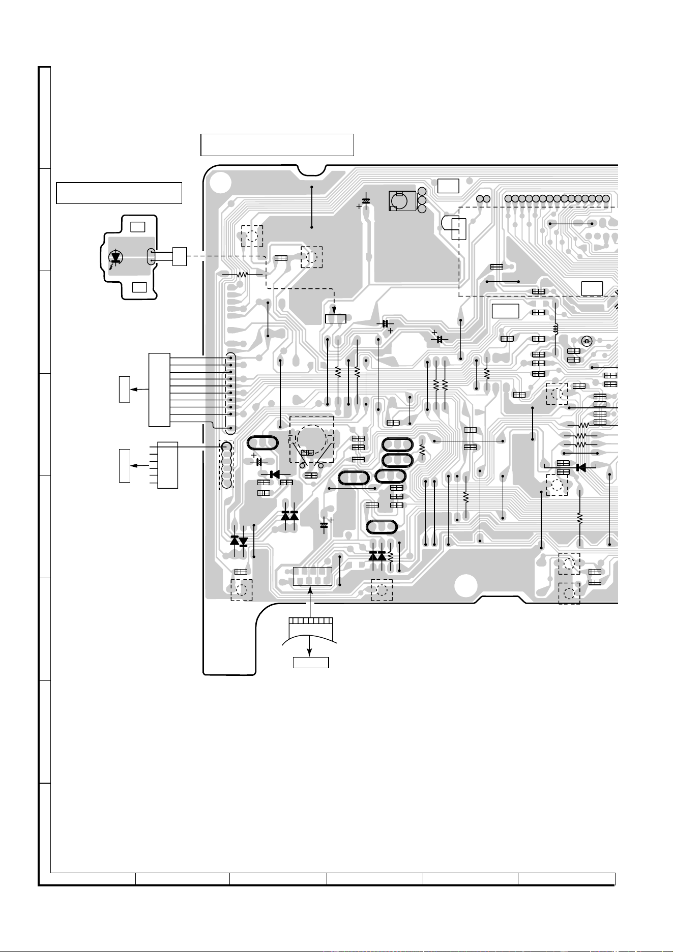
CD-E700H
– 30 –
Figure 30 WIRING SIDE OF P.W.BOARD (3/7)
A
B
C
D
E
F
G
H
1
23456
RD16
RD15
R7
1
R7
1
R7
1
R7
1
RD10
R
R
R763
R702
R708
R705
C704
C721
C705
R709
R710
R769
R780
R791
RD11
RD12
RD21
R779
R778
C715
R777
R781
R782
C710
C709
R775
R776
R756
RD19
BI704
LED704
R739
R737
R717
XL701
FL701
RX701
L701
C702
R706
R703
R704
R728
R759
RD13
CNP702
R740
D710
D709
D711
C712
Q708
D713
D714
Q707
Q706
D715
C714
Q711
Q712
Q709
R783
R795
C701
CNP704
RD20
SW721
X-BASS/DEMO
SW722
EQUALIZER
C717
BI701
D712
1
100
1
2
12
WTM701
FW701
1
6
1
11
10
9
8
7
6
5
4
3
2
1
CNS701
WH
YL
WH
WH
WH
WH
RD
YL
YL
YL
CNP6
TO CD SERVO PWB
P32 3-A
CNP802
TO POWER PWB
P34 4-A
JOG701
JOG VOLUME
SW724
DISC
SKIP
SW723
OPEN/
CLOSE
FFC702
1
7
TO
TAPE MECHANISM PWB
P33 9-A
SW713
VIDEO/
AUX
SW716
PLAY
SW717
FAST
FORWARD
SW712
TUNER
CNS704
BK
BK
1
2
LED B PWB-A5
DISPLAY PWB-A2
191817161514131211109876521
1
3
2
123
123
ECB
ECB
321
ECB
1
2
3
4
5
6
7
D706
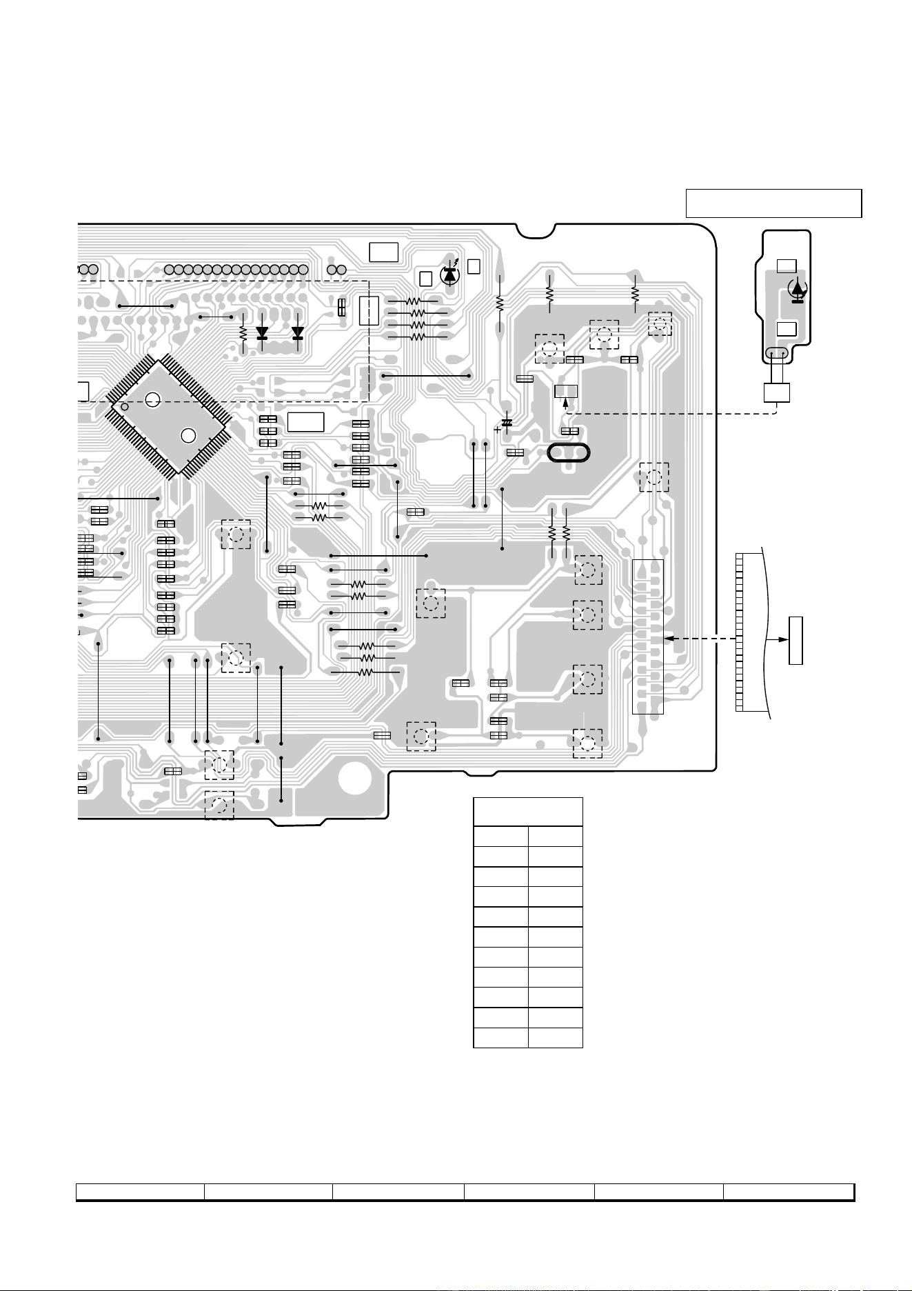
– 31 –
CD-E700H
Figure 31 WIRING SIDE OF P.W.BOARD (4/7)
7
8 9 10 11 12
R751
RD08
RD09
R757
R747
R770
R772
R749
R731
R732
R729
R761
RD06
RD02
RD05
RD04
RD03
D
16
D
15
RD14
R773
R768
R767
R736
R766
R720
R715
R724
R719
R714
R718
R716
R722
R713
C720
R712
R711
R730
R764
R758
R734
R735
IC701
R746
0
4
0
5
CNP701A
RD07
RD01
Q710
CNP703
SW710
DISPLAY
MODE
SW709
ASPM
SW708
PIT
SEARCH
R788
R789
LED701
R745
R794
R744
R743
R742
C707
R727
R726
R733
R765
SW702
MEMORY SET
R725
R762
R721
SW703
REC./PAUSE
R
739
R
737
1
R750
D701
D704
1
30
31
50
51
1
5
10
15
20
25
35
40
45
55
60
65
70
75
80
81
85
90
95
100
1
3
5
7
9
11
13
15
17
19
21
23
2
4
6
8
10
12
14
16
18
20
22
24
12
SW715
STOP
SW718
FAST
REWIND
SW714
TAPE
SW711
CD
SW704
TUNING
DOWN
SW705
TUNING
UP
SW706
TIMER/
SLEEP
SW707
CLOCK
1
FFC701
24
CNP701B
TO MAIN PWB
P29 9-A
SW701
ON/
STAND-BY
BI703
BK
BK
LED703
1
2
CNS703
12
LED A PWB-A4
1918
7
4140 454439383736353433323130292827
321
6
BR
COLOR TABLE
RD(R)
OR
YL
GR
BL
VL
GY
WH(W)
BK
PK
BROWN
RED
ORANGE
YELLOW
GREEN
BLUE
VIOLET
GRAY
WHITE
BLACK
PINK
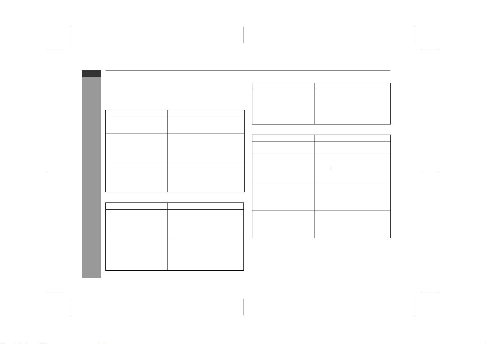
CD-E700H
– 32 –
Figure 32 WIRING SIDE OF P.W.BOARD (5/7)
A
B
C
D
E
F
G
H
1
23456
• The numbers 1 to 12 are waveform numbers shown in page 36.
IC2
R1
R2
C19
C21
C20
R6
R3
R4
R5
C43
C12
R14
R15
R18
R20
C15
C48
R24
C44
R26
C22
R25
R43
R27
IC1
C42
C28
C29
C30
R42
1
5
10
15
20 21
25
30
35
40
41
45
50
55
60
61
65
70
75
80
R10
C33
R11
R12
C27
C8
C45
R40
R39
C4
R9
R41
C38
C2
CNP1
C41
C17
R8
C40
C39
Q4
C9
CNP3
R13
C10
C11
CNP4
R16
C14
R21
R46
C23
C25
L1
C24
C16
XL1
R22
ZD1
CNP5
C26
R32
R33
C5
R34
C6
R35
R36
CNP6
R37
R31
R38
R19
R29
R28
C3
C35
C36
R7
C37
Q1
B
C
E
E
C
B
C1
CNP2
CNS1B
CNS1A
CNS2B
CNS2A
CNS3B
SW4
PICKUP IN
CNP3A
M2
SLED MOTOR
M1
SPINDLE MOTOR
CNS3A
C13
1
5
7
8
10
20
21
22
25
28
14
15
1
1
2
3
4
5
6
7
2
3
4
5
6
7
8
123456 1234567878910
123456654321
BR
COLOR TABLE
RD(R)
OR
YL
GR
BL
VL
GY
WH(W)
BK
PK
BROWN
RED
ORANGE
YELLOW
GREEN
BLUE
VIOLET
GRAY
WHITE
BLACK
PINK
BL
WH
BL
WH
BL
WH
RD
RD
WH
GY
WH
GY
WH
GY
WH
1
2
3
4
5
6
7
8
1
2
3
4
5
6
7
1
2
3
4
5
6
7
8
3
4
1
2
5
6
7
PICKUP UNIT(306)
17
1
8
12345
6
+
–
–
+
RD
WH
GR
WH
GR
WH
12345
6
12345
6
CD MOTOR
PWB-D
CNS701
FROM DISPLAY PWB
P30 1-D
CNS601
FROM MAIN PWB
P29 8-A
CD SERVO PWB-C
3
10
9
4
5
8
7
6
1
2
1211
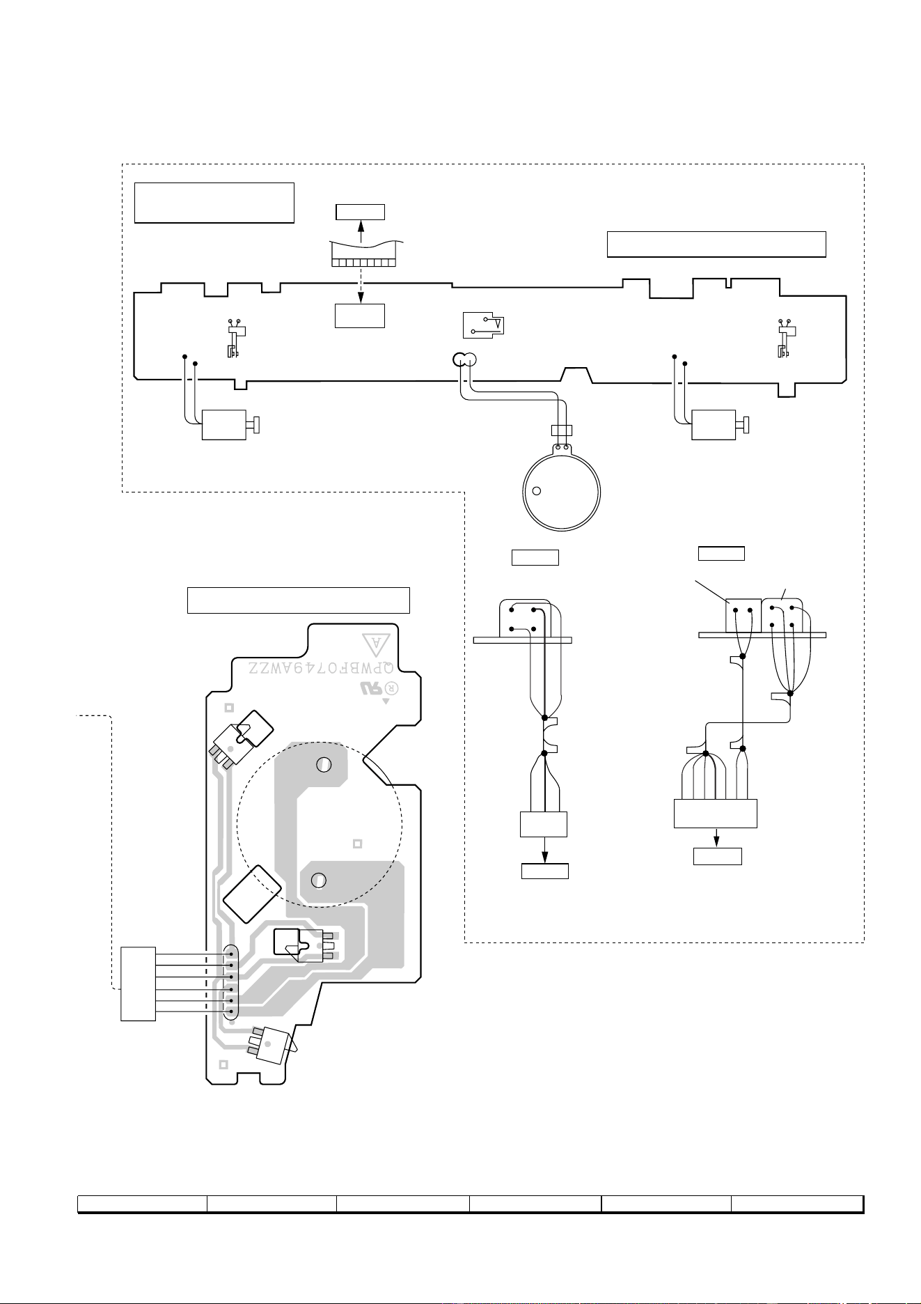
– 33 –
CD-E700H
Figure 33 WIRING SIDE OF P.W.BOARD (6/7)
7
8 9 10 11 12
-
+
BI4
CNS4
FFC702
CD LOADING MOTOR PWB-E
SW1
OPEN/CLOSE
SW3
DISC
NUMBER
SW2
CLAMP
M3
T/T UP/DOWN
LOADING
MOTOR
RD
WH
BK
WH
WH
BK
1
2
3
4
5
6
1
6
–
+
BL
YL
WH
BK
PK
WH
BK
7 6 5 4 3 2 1
PK
BK
WH
23
1
P29 12 - C
TO MAIN PWB
CNP102
CNP101
P29 12 - A
TO MAIN PWB
TAPE 2
ERASE HEAD
RECORD/PLAYBACK
HEAD
TAPE 1
PLAYBACK HEAD
WH
BK
GR
GR
BL
YL
WH
PK
BK
WH
PK
GR
1
2
SW
TAPE
MOTOR
SOLENOID
TAPE MECHANISM PWB-F
SW
SOLENOID
SW
TAPE MECHANISM
ASSEMBLY
1
2
3
4
5
6
7
1
7
CNP702
P30 3-F
TO DISPLAY PWB
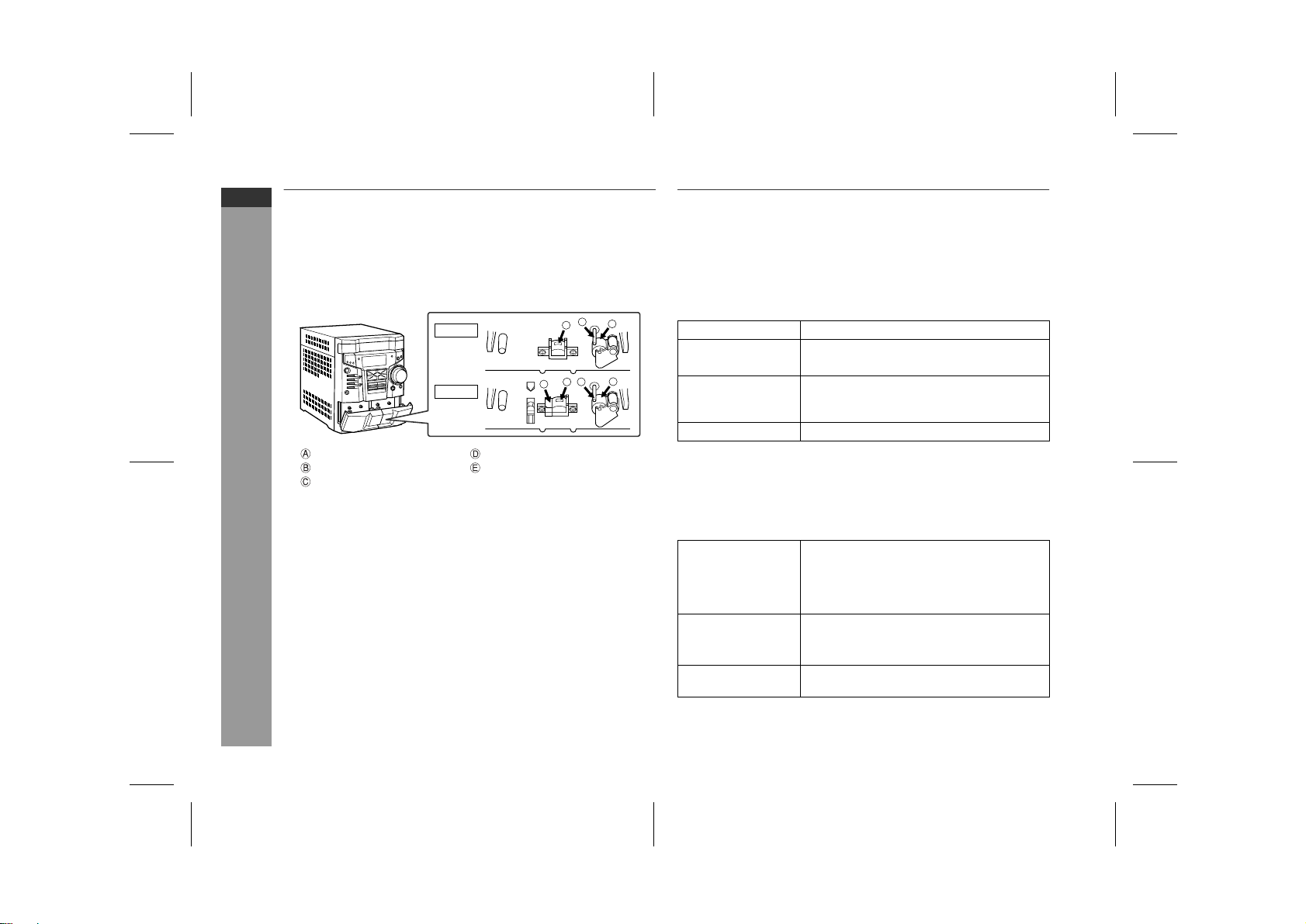
CD-E700H
– 34 –
Figure 34 WIRING SIDE OF P.W.BOARD (7/7)
A
B
C
D
E
F
G
H
1
23456
When Servicing, pay attention as the area
enclosed by this line ( ) is directly
connected with AC main voltage.
R842
C808
C809
D801
D802
CNP801
C804
R803
C801
R804
C802
ZD801
R806
D806
Q801
R808
C803
ZD803
R844
R805
R801
R802
D804
D803
D805
C807
C806
C805
ZD802
C842
Q841
R843
C841
D842
D843
D844
D845
R858
C861
C843
IC854
D856
D853
R841
RL841
C844
L841
CNP802
CNP805
CNS805
D846
1
12345678910
23456
14
T.F.
PT801
MAIN POWER
TRANSFORMER
WTM802
FW802
WTM801
14
TRANSFORMER PWB-B2
PT841
SUB POWER TRANSFORMER
AC POWER
SUPPLY CORD
AC 230 V, 50 Hz
FW701
FROM DISPLAY PWB
P30 1-D
CNS801
FROM MAIN PWB
P29 12-G
POWER PWB-B1
C811
C810
F802
T4A L 250V
F801
T4A L 250V
F803
T2A L 250V
F804
T2A L 250V
F805
T2A L 250V
3
BCE
ECB
21
1
2
1
2
BL
BL
BR
BR
BR
COLOR TABLE
RD(R)
OR
YL
GR
BL
VL
GY
WH(W)
BK
PK
BROWN
RED
ORANGE
YELLOW
GREEN
BLUE
VIOLET
GRAY
WHITE
BLACK
PINK
– 35 –
CD-E700H
VOLTAGE
PIN NO. VOLTAGE PIN NO. VOLTAGE PIN NO. VOLTAGE PIN NO. VOLTAGE PIN NO. VOLTAGE
10 V
0 V
0 V1
2
1 1.6 V 1 4.85 V 51 4.93 V
PIN NO. VOLTAGE
20 V
0 V
2
3
4
1.0 V 2 4.78 V
0 V
52
53
54
4.93 V
1
2
3
7.76 V
3 0.56 V 3
5
1.6 V 3
0 V
4 1.996 V
N.C.
4 5 V 1.8 V 4
0 V
2 V
2 V
2 V
2 V
55 V
5 V
5
6
3.3 V 5 4.71 V
0 V
55 0 V
0 V
N.C.
4
6 1.303 V
0 V
6
7
0 V 6 4.75 V 56 0 V
5
75 V
5 V
5 V
7
8
9
1.6 V 7 4.78 V 57 0 V
6
8 0.587 V 8 1.6 V 8 4.92 V
0 V
58
59
0 V
0 V
7
8
9 3.54 V 9 1.6 V 9
2 V
2 V
10 3.46 V 10 5 V 10 1.6 V 10 4.89 V 60 0 V
9
11 0 V 11 5 V 11 1.6 V 11 2.32 V 61 0 V
10 2 V
12 0 V 12 5 V 12 1.6 V 12 2.014 V 62 0 V
11 2 V
13 7.03 V 13 5 V 13 1.5 V 13 0 V 63 4.82 V
12 4.8 V
14 4.2 V 14 5 V 14 1.5 V 14 4.78 V 64 4.84 V
13 1.7 V
15 0 V 15 5 V 15 1.5 V 15 0 V 65 4.84 V
14 1.7 V
16 3.46 V 16 5 V 16 1.5 V 16 4.79 V 66 4.82 V
15 1.7 V
17 0.587 V 17 5 V 17 0.8 V 17 4.72 V 67 0 V
16 1.7 V
18 0 V 18 5 V 18 3.2 V 18 0.14 V 68 4.82 V
17 1.7 V
19 2.68 V 19 5 V 19 0 V 19 4.86 V 69 -27.4 V
18 1.7 V
20 N.C. 20 5 V 20 1.6 V 20 0.1 V 70 -30.4 V
19 4 V
21 2.02 V 21 5 V 21 1.6 V 21 0 V 71 -30.4 V
20 3.3 V
22 0.561 V 22 5 V 22 1.6 V 22 0 V 72 -18.2 V
21 1.7 V
23 0 V 23 10.07 V 23 1.6 V 23 0 V 73 -30.4 V
22 4.8 V
24 0 V 24 0 V 24 0 V 24 5.02 V 74 -27.4 V
23 1.7 V
25 0 V 25 0 V 75 -21.1 V
24 1.7 V
26 3.2 V 26 4.93 V 76 -24.2 V
25 2.8 V
27 0 V 27 0. V 77 -27.3 V
26 0 V
PIN NO. VOLTAGE 28 0 V 28 5.08 V 78 -15.13 V
27 4.8 V
PIN NO. VOLTAGE 1 2.13 V 29 0 V 29 5.07 V 79 -30.5 V
28 4.8 V
1 20.2 V 2 5.15 V 30 0 V 30 0 V 80 -27.3 V
2 1.351 V 3 2.13 V 31 0 V 31 5.08 V 81 -18.23 V
3 13.41 V 4 2.13 V
0 V
32
33
0 V
0 V
32
33
3.31 V 82 -27.3 V
5 5.08 V 83 -24.2 V
6 5.23 V 34 0 V 34 4.79 V 84 -30.4 V
7 5.23 V 35 0 V 35 5.08 V 85 -21.2 V
PIN NO. VOLTAGE 8 3.6 V 36 0 V 36 1.41 V 86 -14.95 V
1 19.9 V
0 V
9
10
5.15 V 37 0 V 37 0 V 87 -30.4 V
2 4.43 V 38 3.2 V 38 5.09 V 88 -30.3 V
3 10.09 V 11 1.836 V 39 3.2 V 39 4.95 V 89 -30.3 V
12 1.265 V 40 0 V 40 0 V 90 -30.3 V
13 2.32 V 41 3.7 V 41 0 V 91 -27.2 V
14 1.25 V 42 3.7 V 42 13.23 V 92 -27.2 V
PIN NO. VOLTAGE 15 1.269 V 43 0 V 43 13.23 V 93 -27.1 V
1 20.4 V
0 V
5 V
16
17
18
2.12 V
0 V
44
45
0 V 44 13.23 V 94 -27.3 V
3 3.7 V 45 3.82 V 95 -27.3 V
2 5.01 V 46 3.2 V 46 4.79 V 96 -27.3 V
19 5.02 V 47 3.2 V 47 4.78 V 97 -26.6 V
20 5.02 V 48 3.2 V 48 4.54 V 98 -27.3 V
PIN NO. VOLTAGE 21 5.04 V 49 0 V 49 0 V 99 -27.3 V
1 15.5 V 22 5.04 V 50 0 V 50 4.93 V 100 -27.3 V
2 0.59 V 23 10.08 V 51 0 V
3 5.6 V 24 0 V 52 3.2 V IC901
53 0 V PIN NO. VOLTAGE
54 0 V 1 58.8 V
PIN NO. VOLTAGE PIN NO. VOLTAGE 55 0 V 2 27.8 V
1 2.6 V
0 V
0 V
0 V
0 V
1
2
3
4
5
0.8 V 56 0 V 3 15.9 V
2 1.5 V 57 0 V 4 -15.9 V
0 V
0 V
0 V
3 3.6 V 58 3.2 V 5 28.2 V
4 1.5 V 59 0 V 6 -58.7 V
50 V600 V7
6 5.07 V 6 3.6 V 61 0 V 8
7 10.05 V 7 2.8 V 62 4.7 V 9
8 4.78 V
0 V
8
9
3.6 V 63 0 V 10 0 V
9 3.6 V 64 4.9 V 11 0 V
10 0 V 65 4.9 V 12 -56.8 V
11 5.23 V 66 4.9 V 13 -56.8 V
12 0 V 67 0 V 14 0 V
13 5.23 V 68 4.9 V 15 0 V
14 0 V PIN NO. VOLTAGE 69 0 V 16 -55.3 V
15 0 V E 7.69 V 70 0 V 17 0 V
16 2.6 V B 8.24 V 71 0 V 18 0 V
17 5.25 V C 13.2V 72 0 V
18 0 V 73 0 V
19 0 V 74 0 V
20 0.838 V 75 0 V
21 0 V 76 3.2 V
22 2.71 V 77 3.2 V
78 3.2 V
79 0 V
80 3.2 V
IC2
IC601 IC1 IC701IC101
IC302
IC303
IC301
IC855
IC852
IC851
IC854
IC853
ICT21
PIN NO. VOLTAGE
1 2.58 V
2 2.58 V
3 15.19 V
40 V
0 V
5 2.58 V
6 2.58 V
2.67 V
2.67 V
7
8
9
10 0 V
11 5.19 V
12 5.19 V
13 -56.8 V
14 0 V
15 0 V
16 0 V
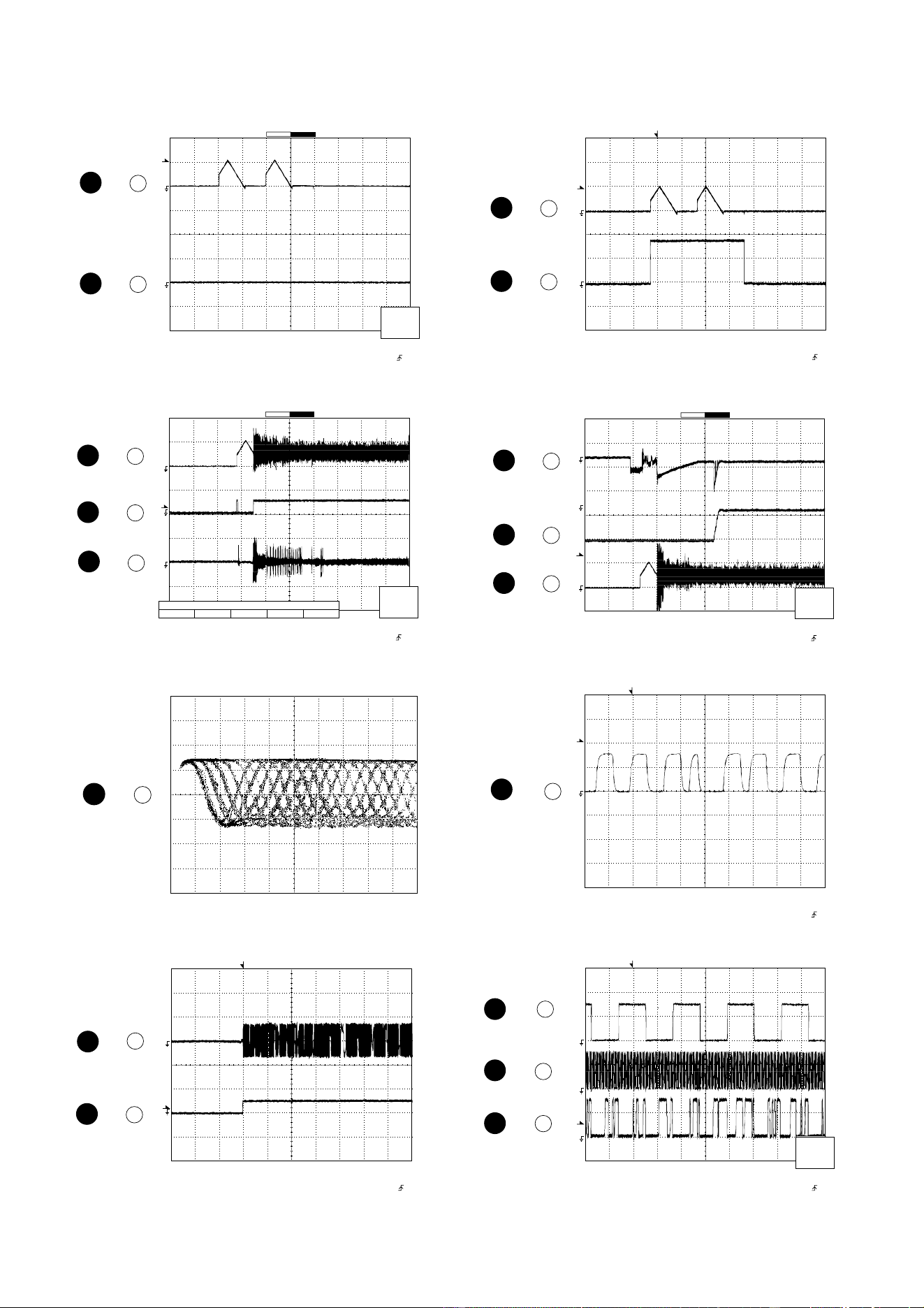
CD-E700H
– 36 –
T
T
DATA
DATACK
LRSY
Stopped
CH1=2 V
DC 10:1
CH2=2 V
DC 10:1
CH3=2 V
DC 10:1
5 µs/div
(5 µs/div)
NORM:100 kS/s
1
2
3
=Record Length=
Smoothing : ON CH1 : 0.00 V
CH2 : 0.00 V
Main : 5 K
Zoom : 100
Mode : AUTO
Type : EDGE CH3
Delay : 0.0 ns
Hold off : 0.2 µs
CH3 : 0.00 V
CH4 : 0.00 V
BW : FULL
=Trigger==Filter= =Offset=
CH3
v/DIV
2 V
1999/04/05 20:50:17
10
IC1 58
IC1 59
IC1 60
11
12
T
T
DOUT
Stopped
CH1=2 V
DC 10:1
500 ns/div
1999/04/07 09:25:28
(500 ns/div)
NORM:200 MS/s
1
=Record Length=
Smoothing : ON CH1 : 0.00 V
CH2 : 0.00 V
Main : 1 K
Zoom : 100
Mode : NORMAL
Type : EDGE CH1
Delay : 2.887 ms
Hold off : 0.2 µs
CH3 : 0.00 V
CH4 : 0.00 V
BW : FULL
=Trigger=
=Filter= =Offset=
9
IC1 39
T
FDO
PDO2
PDO1
Stopped
CH1=500 mV
DC 10:1
CH3=1 V
DC 10:1
CH4=1 V
DC 10:1
500 ms/div
(500 ms/div)
NORM:20 kS/s
1
4
3
=Record Length=
Smoothing : ON CH1 : 0.000 V
CH2 : 0.0 V
Main : 100 K
Zoom : 2 K
Mode : AUTO
Type : EDGE CH2
Delay : 0.0 ns
Hold off : 0.2 µs
CH3 : 0.00 V
CH4 : 0.00 V
BW : FULL
=Trigger==Filter= =Offset=
CH1
v/DIV
500 mV
1999/04/05 17:33:17
1
IC1 21
7
IC1 73
8
IC1 74
T
T
FDO
SPDO
Stopped
CH1=200 mV
DC 10:1
CH2=500 mV
DC 10:1
500 ms/div
1999/04/07 09:51:15
(500 ms/div)
NORM:20 kS/s
2
1
=Record Length=
Smoothing : ON CH1 : 0.000 V
CH2 : 0.000 V
Main : 100 K
Zoom : 2 K
Mode : NORMAL
Type : EDGE CH2
Delay : 2.924 ms
Hold off : 0.2 µs
CH3 : 0.00 V
CH4 : 0.00 V
BW : FULL
=Trigger=
=Filter= =Offset=
1
IC1 21
6
IC1 22
T
T
TE
DRF
Stopped
CH1=10 V
DC 10:1
CH2=1 V
DC 10:1
100 ms/div
(100 ms/div)
NORM:100 kS/s
2
1
=Record Length=
Smoothing : ON CH1 : 0.0 V
CH2 : 0.00 V
Main : 100 K
Zoom : 2 K
Mode : NORMAL
Type : EDGE CH1
Delay : 2.924 ms
Hold off : 0.2 µs
CH3 : 0.00 V
CH4 : 0.00 V
BW : FULL
=Trigger=
=Filter= =Offset=
3
IC1 67
4
IC1 15
Vp-p=1.0 V~1.3 V
0.5 mV/div,0.5 µsec/div
5
IC1 4
T
FDO
DRF
TE
Stopped
CH1=500 mV
DC 10:1
CH2=10 V
DC 10:1
CH3=1 V
DC 10:1
500 ms/div
(500 ms/div)
NORM:20 kS/s
1
2
3
=Record Length=
Smoothing : ON CH1 : 0.000 V
CH2 : 0.0 V
Main : 100 K
Zoom : 2 K
Mode : AUTO
Type : EDGE CH1
Delay : 0.0 ns
Hold off : 0.2 µs
CH3 : 0.00 V
CH4 : 0.00 V
BW : FULL
=Trigger==Filter= =Offset=
-3 div -1 div 0 div +1 div +3 div
CH Position To
CH2
Position
0.20 div
1
IC1 21
3
IC1 67
4
IC1 15
T
FDO
TDO
Stopped
CH1=500 mV
DC 10:1
CH3=500 mV
DC 10:1
500 ms/div
(500 ms/div)
NORM:20 kS/s
1
3
=Record Length=
Smoothing : ON CH1 : 0.000 V
CH2 : 0.0 V
Main : 100 K
Zoom : 2 K
Mode : AUTO
Type : EDGE CH1
Delay : 0.0 ns
Hold off : 0.2 µs
CH3 : 0.000 V
CH4 : 0.00 V
BW : FULL
=Trigger==Filter= =Offset=
CH1
v/DIV
500 mV
1
IC1 21
2
IC1 20
WAVEFORMS OF CD CIRCUIT

– 37 –
CD-E700H
HOW TO USE
CAUTION
Cleaning fluid
Cleaner disc
Using the brush in the cleaner cap, apply 1 or 2 drops of the cleaning fluid to the
brush on the CD cleaner disc which has the mark next to it.
Place the CD cleaner disc onto the CD disc tray with the brush side down,then
press the play button.
You will hear music for about 20 seconds and the CD player will automatically stop.
If it continuous to turn, press the stop button.
1.
2.
3.
The CD lens cleaner should be effective for 30-50 operations, however if the
brushes become worn out earlier then please the cleaner disc.
If the CD cleaner brushes become very wet then wipe off any excess fluid with a soft
cloth.
Do not drink the cleaner fluid or allow it to come in contact with the eyes. In the
event of this happening then drink and / or rinse with clean water and seek medical
advice.
The CD cleaner disc must not be used on car CD players or on computer CD-ROM
drives.
All rights reserved. Unauthorized duplicating, broadcasting and renting this product
is prohibited by law.
Parts code
1. CD optical pickup Lens cleaner disc UDSKA0004AFZZ
TROUBLESHOOTING
When the CD does not function
When the CD section does not operate when the objective lens of the optical pickup is dirty, this section may not operate. Clean
the objective lens, and check the playback operation. When this section does not operate even after the above step is taken, check
the following items.
Remove the cabinet and follow the trouble shooting instructions.
"Track skipping and/or no TOC (Table Of Contents) may be caused by build up of dust other foreign matter on the laser pickup
lens. Before attempting any adjustment make certain that the lens is clean. If not, clean it as mentioned below."
Turn the power off.
Gently clean the lens with a lens cleaning tissue and a small amount of isopropyl alcohol.
Do not touch the lens with the bare hand.
When a CD cannot be played
1. "E-CD01" is displayed.
(1) Check the power to IC1 (LC78646E), the presence of the clock signal (16.933 MHz) and the status of the RESET terminal
(pin 66 on IC1).
(2) Does the pickup move to the PICKUP-IN Switch (SW4) position?
If (1) and (2) are OK, check the system microcomputer (especially the communication line with the DSP).
2. Pressing the CD operation key is accepted, but playback does not occur.
(1) Focus-HF system check
(2) Tracking system check
(3) Spin system check
(4) PLL system check
(5) Others
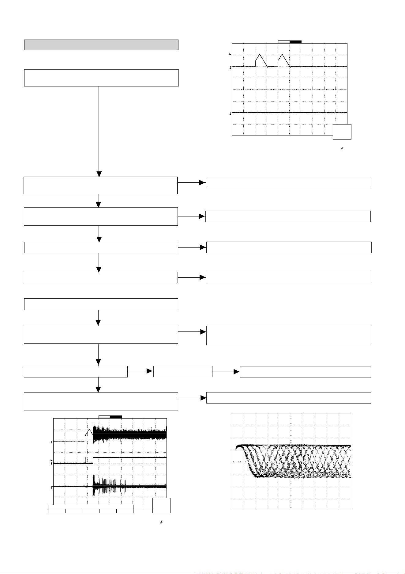
CD-E700H
– 38 –
Vp-p=1.0 V~1.3 V
0.5 mV/div,0.5 µsec/div
T
FDO
DRF
TE
Stopped
CH1=500 mV
DC 10:1
CH2=10 V
DC 10:1
CH3=1 V
DC 10:1
500 ms/div
(500 ms/div)
NORM:20 kS/s
1
2
3
=Record Length=
Smoothing : ON CH1 : 0.000 V
CH2 : 0.0 V
Main : 100 K
Zoom : 2 K
Mode : AUTO
Type : EDGE CH1
Delay : 0.0 ns
Hold off : 0.2 µs
CH3 : 0.00 V
CH4 : 0.00 V
BW : FULL
=Trigger==Filter= =Offset=
-3 div -1 div 0 div +1 div +3 div
CH Position To
CH2
Position
0.20 div
T
FDO
TDO
Stopped
CH1=500 mV
DC 10:1
CH3=500 mV
DC 10:1
500 ms/div
(500 ms/div)
NORM:20 kS/s
1
3
=Record Length=
Smoothing : ON CH1 : 0.000 V
CH2 : 0.0 V
Main : 100 K
Zoom : 2 K
Mode : AUTO
Type : EDGE CH1
Delay : 0.0 ns
Hold off : 0.2 µs
CH3 : 0.000 V
CH4 : 0.00 V
BW : FULL
=Trigger==Filter= =Offset=
CH1
v/DIV
500 mV
If the level is not normal.
1. Is focus servo activated ?
(Waveform drawing Figure 38-2)
Pins 7~11, 79 and 80 on IC1
Check the laser diode driver Q1 peripheral circuit.
When a disc is loaded, start playback operation.
2. Does DRF change from "L" to "H" ?
Is the disc rotating ?
3. Is the HF waveform normal ?
(Waveform drawing Figure 38-3)
Check the spin system.
If the disc is spinning and a HF waveform is generated,
DRF will go H.
Figure 38-1
Check the laser diode driver Q1 peripheral circuit.
(1) Focus-HF system check.
Although a CD is inserted and the cover is closed, "NO
DISC" is displayed.
1. Does the pickup move to the PICKUP-IN Switch (SW4)
position ?
Sled motor (M2).
Press the OPEN/CLOSE switch (SW1) without inserting a
disc, and try starting the playback operation.
2. Does the focus (lens) move up and down ?
(Waveform drawing Figure 38-1)
Check the focus peripheral circuit.
3. Is the laser lit ?
Spindle motor (M1).
4. Is the turntable rotating ?
Figure 38-2
Figure 38-3
Yes
Yes
Yes
No
No
No
No
No
No
No
Yes
Yes
No
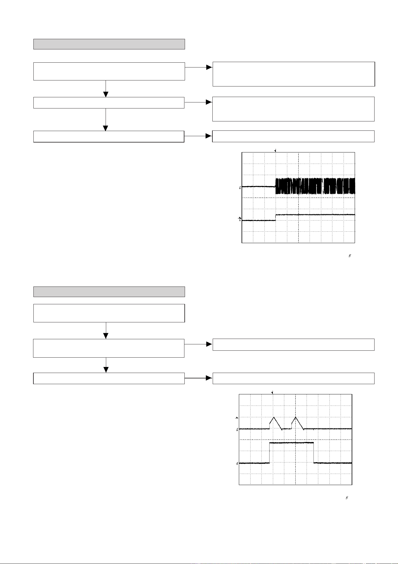
– 39 –
CD-E700H
T
T
FDO
SPDO
Stopped
CH1=200 mV
DC 10:1
CH2=500 mV
DC 10:1
500 ms/div
1999/04/07 09:51:15
(500 ms/div)
NORM:20 kS/s
2
1
=Record Length=
Smoothing : ON CH1 : 0.000 V
CH2 : 0.000 V
Main : 100 K
Zoom : 2 K
Mode : NORMAL
Type : EDGE CH2
Delay : 2.924 ms
Hold off : 0.2 µs
CH3 : 0.00 V
CH4 : 0.00 V
BW : FULL
=Trigger=
=Filter= =Offset=
T
T
TE
DRF
Stopped
CH1=10 V
DC 10:1
CH2=1 V
DC 10:1
100 ms/div
(100 ms/div)
NORM:100 kS/s
2
1
=Record Length=
Smoothing : ON CH1 : 0.0 V
CH2 : 0.00 V
Main : 100 K
Zoom : 2 K
Mode : NORMAL
Type : EDGE CH1
Delay : 2.924 ms
Hold off : 0.2 µs
CH3 : 0.00 V
CH4 : 0.00 V
BW : FULL
=Trigger=
=Filter= =Offset=
The tracking servo is not activated.
Check the peripheral circuits at pins 14, 15 and 20 on IC1, and
CNS1A/B.
If the waveform shown in Figure 39-1 appears and soon after
NO DISC appears ?
(2) Tracking system check.
Check the TE waveform at pin 15 on IC1.
A normal jump operation cannot be completed or the beginning of
the track cannot be found.
Check the around pin 20 on IC1.
"Initialization" is possible, but play is not possible ?
Data cannot be read. Check the VCO-PLL system.
"Initialization" is not possible.
Figure 39-1
Figure 39-2
Press the OPEN/CLOSE switch without inserting a disc, and
then try starting the play operation.
(3) Spin system check.
The spin driver circuit is OK.
1. The turntable rotates a little ?
(Waveform drawing Figure 39-2)
Check around pin 22 on IC1, pins 15 and 16 on IC2, and CNS3A/B.
2. The turntable doesn't rotate.
No
Yes
No
Yes
Yes
No
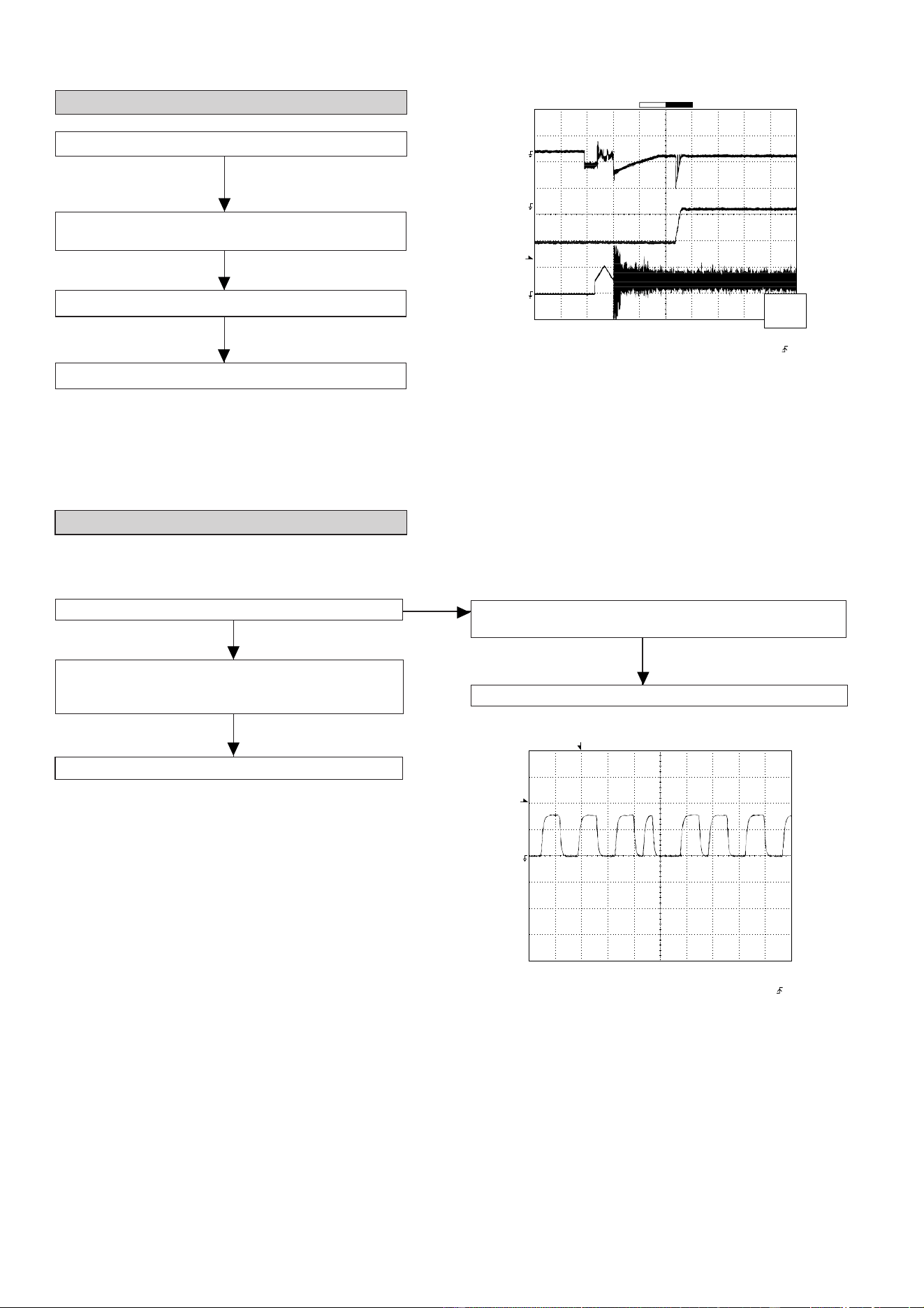
CD-E700H
– 40 –
T
T
DOUT
Stopped
CH1=2 V
DC 10:1
500 ns/div
1999/04/07 09:25:28
(500 ns/div)
NORM:200 MS/s
1
=Record Length=
Smoothing : ON CH1 : 0.00 V
CH2 : 0.00 V
Main : 1 K
Zoom : 100
Mode : NORMAL
Type : EDGE CH1
Delay : 2.887 ms
Hold off : 0.2 µs
CH3 : 0.00 V
CH4 : 0.00 V
BW : FULL
=Trigger=
=Filter= =Offset=
T
FDO
PDO2
PDO1
Stopped
CH1=500 mV
DC 10:1
CH3=1 V
DC 10:1
CH4=1 V
DC 10:1
500 ms/div
(500 ms/div)
NORM:20 kS/s
1
4
3
=Record Length=
Smoothing : ON CH1 : 0.000 V
CH2 : 0.0 V
Main : 100 K
Zoom : 2 K
Mode : AUTO
Type : EDGE CH2
Delay : 0.0 ns
Hold off : 0.2 µs
CH3 : 0.00 V
CH4 : 0.00 V
BW : FULL
=Trigger==Filter= =Offset=
CH1
v/DIV
500 mV
1999/04/05 17:33:17
Is pin 52 (C2F) on IC1 "L" ?
Yes
No
The HF waveform is normal and the time is displayed
normally, but no sound is produced. Or the sound
has dropouts.
(5) Others.
There are too many error flags on a damaged disc which
makes error correction impossible.
Check again using a known good disc.
1. When playing at normal speed
Check the peripheral circuit at pin 39 (DOUT) on IC1 and
the waveform (Figure 40-2).
If OK, Check the unit.
When a disc is loaded, start play operation.
(4) PLL system check.
The HF waveform is normal, but the TOC data cannot be
read.
Check the PDO waveform. (Figure 40-1)
Check around pins 73~78 on IC1.
Figure 40-1
Figure 40-2
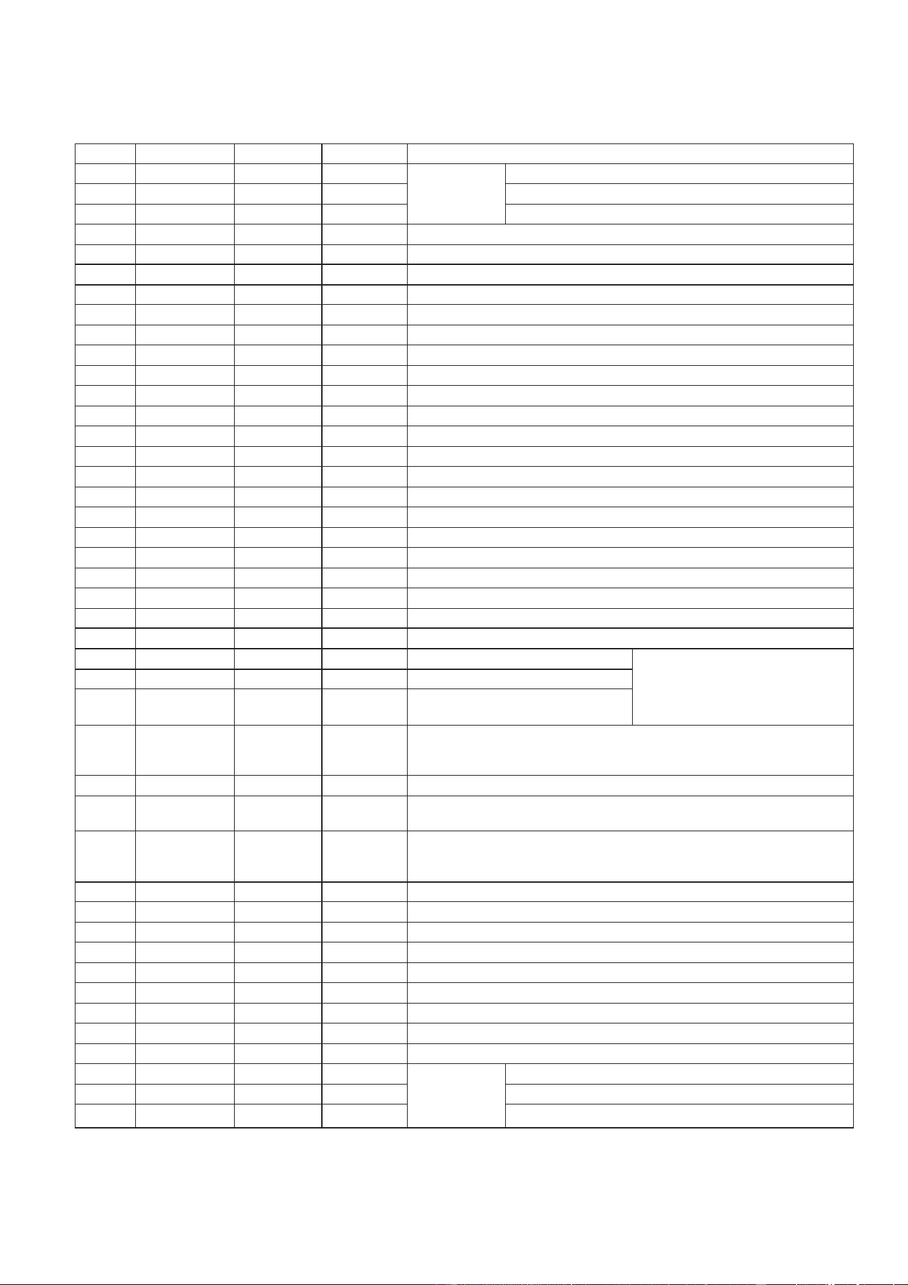
– 41 –
CD-E700H
FUNCTION TABLE OF IC
IC1 VHiLC78646E-1: CD Servo (LC78646E) (1/2)
1 SLCO Output — Control output.
2 SLCIST Input —
Resistor connection terminal for SLCO output current
setting.
3 EFMIN Input — RF signal input terminal.
4 RF Output — RF signal monitor terminal.
5 RFVDD Input — RF power terminal.
6 RFVSS — — RF earth terminal. To be connected to 0 V.
7 FIN1 Input — A+C signal input terminal.
8 FIN2 Input — B+D signal input terminal.
9 TIN1 Input — E signal input terminal.
10 TIN2 Input — F signal input terminal.
11 VREF Output RFVDD/2 VREF voltage output terminal.
12 REF1 Input — Reference supply setting terminal.
13* FE Output ZHI FE signal monitor terminal.
14 TEC Output — LPF capacitor connection terminal for TE signal.
15* TE Output ZHI TE signal monitor terminal.
16* RFMON Output ZHI RF internal signal monitor terminal.
17 JITTC — — Capacitor connection terminal for jitter detection.
18 ADAVDD Input — Power terminal for servo A/D, D/A.
19 ADAVSS — — Earth terminal for serve A/D, D/A. To be connected to 0 V.
20 TDO Output ADAVDD/2 Output terminal for tracking control. D/A output.
21 FDO Output ADAVDD/2 Output terminal for focus control. D/A output.
22 SPDO Output ADAVDD/2 Output terminal for spindle control. D/A output.
23 SLDO Output ADAVDD/2 Output terminal for sled control. D/A output.
24* GPDAC Output ADAVDD/2 Servo D/A general-purpose output terminal.
25* CONT4 Input/Output Input Mode General-purpose I/O terminal 4.
26 CONT5 Input/Output Input Mode General-purpose I/O terminal 5.
27* SBCK/CONT6 Input/Output Input Mode General-purpose I/O terminal 6 or
Subcode reading clock input terminal.
28 SBCK/FG Input — Subcode reading clock input terminal/FG signal input terminal/external
emphasis setting terminal. Terminal functions are set by commands. When
not used, connect to 0 V.
29* DEFECT Output L Defect terminal.
30* V/*P Output H Auto switching monitor output terminal for rough servo phase control. “H”:
rough servo, “L”: phase servo.
31* FSEQ Output L Sync signal detection output terminal.
The status changes to “H” when the sync signal detected in EFM and the
sync signal of internal generation are identified.
32* MONI1 Output L Internal signal monitor terminal 1.
33* MONI2 Output L Internal signal monitor terminal 2.
34* MONI3 Output L Internal signal monitor terminal 3.
35* MONI4 Output L Internal signal monitor terminal 4.
36* MONI5 Output L Internal signal monitor terminal 5.
37 VSS — — Digital system earth terminal. To be connected to 0 V.
38 VDD Input — Digital system power terminal.
39* DOUT Output L Digital OUT output terminal. (EIAJ format)
40 TEST Input L Input terminal for test. To be connected to 0 V.
41 LVDD Input — Power supply for Left channel.
42 LCHO Output LVDD/2 Left channel output.
43 LVSS — — GND for Left channel. Must be connected to 0 V.
Pin No. FunctionTerminal Name
Input/Output
Setting in Reset
In this unit, the terminal with asterisk mark (*) is (open) terminal which is not connected to the outside.
Left channel
D/A converter
For slice level
control.
Controlled by commands from the
microcomputer. When not used, set
them as input terminals and connect
to 0 V, or set them as output
terminals and leave open.

CD-E700H
– 42 –
44 RVSS — — GND for Right channel. Must be connected to 0 V.
45 RCHO Output LVDD /2 Right channel output.
46 RVDD Input — Power supply for Right channel.
47 XVDD Input — Power supply for crystal oscillator.
48 XOUT Output — Connected for the 33.8688 MHz crystal oscillator ciement.
49 XIN Input —
50 FSX/16MIN Input/Output Input 7.35 kHz Synchronization signal monitor port.
or Clock input port for Digital filter & D/A
51 XVSS — — Crystal GND for crystal oscillator. Must be connected to 0 V.
Oscillator
52* C2F Output H C2 FLAG monitor port.
53* EFLG Output L C1, C2 error corrected monitor port.
54* 16MOUT Output Clock 16.9344 MHz output port.
55 ASLRCK Input — Word clock input port.
(If this port does not use, must be connect to 0 V.)
56 ASDACK Input — Bit clock input port.
(If this port does not use, must be connect to 0 V.)
57 ASDFIN Input —
Left/Right channel data input port.
(If this port does not use, must be connect to 0 V.)
58* LRCK Output L Word clock output port.
59* BCK Output L Digital data Bit clock output port.
60* DATA Output L Left/Right channel data output port.
61 CE Input — Chip enable signal input port.
62 CL Input —
Microcomputer
Data transfer clock input port.
63 DI Input — Interface Data input port.
64 DO Output (H) Data output port. (N-ch. open drain output.)
65 *WRQ Output H Interruption signal output.
66 *RES Input — Chip reset signal input port.
This port must be set LOW after first applied power on.
67 DRF Output L Focus detection output port.
68 VDD5 Input — Power supply for Microprocessor.
69 VSS — — GND for digital circuit. Must be connected to 0 V.
70 CONT3 Input/Output Input General purpose port 1.
71 CONT2 Input/Output Input General purpose port 2.
72 CONT1 Input/Output Input General purpose port 3.
73 PDO1 Output — Internal VCO control phase comparator output port 1.
74 PDO2 Output Input Internal VCO control phase comparator output port 2.
75 VVSS — — GND for internal VCO. Must be connected to 0 V.
76 PCKIST Input — PDO output current adjustment resistor connection port.
77 VVDD Input — Power supply for internal VCO.
78 FR Input — VCO frequency range adjustment port.
79 LDS Input — LASER power detected signal input port.
80 LDD Output — LASER power control signal output port.
IC1 VHiLC78646E-1: CD Servo (LC78646E) (2/2)
Pin No.
Function
Terminal Name
Input/Output
Setting in Reset
Right channel
D/A converter
Crystal
Oscillator
Anti-shock
Controlled with serial data command from micro-
computer. When not used, General purpose input/
output terminal 7. set it as the input terminal and open
it by connecting to 0 V, or set it as the output terminal
and open it.
PLL
In this unit, the terminal with asterisk mark (*) is (open) terminal which is not connected to the outside.
Be sure to supply the same potential to each power terminal. (VVDD, ADAVDD, VDD, LVDD, RVDD, XVDD)
Terminal witch is controlled by the power terminal (VDD5 V) for a microcomputer interface :
CE (61 pin), CL (62 pin), DI (63 pin), DO (64 pin), WRQ (65 pin), RES (66 pin), DRF (67 pin)
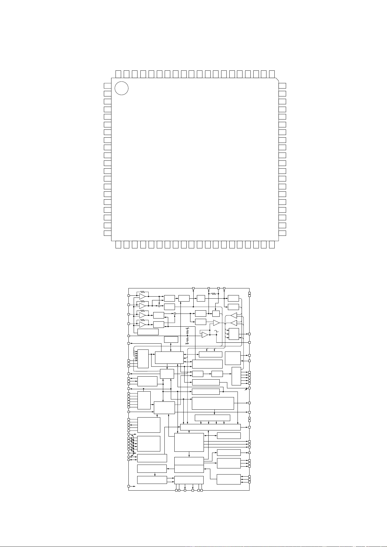
– 43 –
CD-E700H
Figure 43 BLOCK DIAGRAM OF IC
IC1 VHiLC78646E-1: CD Servo (LC78646E)
1
2
3
4
5
6
7
8
9
10
11
12
13
14
15
16
17
18
19
20
21 22 23 24 25 26 27 28 29 30 31 32 33 34 35 36 37 38 39 40
80 79 78 77 76 75 74 73 72 71 70 69 68 67 66 65 64 63 62 61
60
59
58
57
56
55
54
53
52
51
50
49
48
47
46
45
44
43
42
41
SLCO
SLCIST
EFMIN
RF
RFVDD
RFVSS
FIN1
FIN2
TIN1
TIN2
VREF
REF1
FE
TEC
TE
RFMON
JITTC
ADAVDD
ADAVSS
TDO
FDO
SPDO
SLDO
GPDAC
CONT4
CONT5
SBCK/CONT6
SBCK/FG
DEFECT
V/*P
FSEQ
MONI1
MONI2
MONI3
MONI4
MONI5
(3.3V)VSS
VDD
DOUT
TEST
LDD
LDS
FR
VVDD
PCKIST
VVSS
PD02
PD01
CONT1
CONT2
CONT3
VSS
VDD5
DRF
*RES
*WRQ
DO
DI
CL
CE
DATA
BCK
LRCK
ASDFIN
ASDACK
ASLRCK
16MOUT
EFLG
C2F
XVSS
FSX/16MIN
XIN
XOUT
XVDD
RVDD
RCHO
RVSS
LVSS
LCHO
LVDD
LC78646E
+
–
+
–
+
–
+
–
–
–
+
+
MIX
LPF
LPF
LPF
TBAL
TBAL
RAM
LEVEL SET
AGC EQ
SW
PH
BH
+
–
+
–
+
–
+
–
MONI
CONT
A/D
SERVO PROCESSOR
TRACK JUMP
AUTO ADJUST
JITTER
DETECT
1bit DAC
8FS
DIGITAL FILTER
GENERAL-PURPOSE
PORTS
COMMAND
INTERFACE
CLOCK
GENERATOR
CLV,CAV
CONTROL
PLL
VCEC
SLICE LEVEL
CONTROL
APC
S/H
D/A
SW
DRF
RUPTURE DEFECT
FRAME SYNC
DETECT,PROTECT INSERT,
EFN DECODE
VDD
SUBCODE DECODE CRC
MONITOR SIGNAL SELECTOR
RAM
ERROR
CORRECTION
AUDIO CD
AUDIO OUT
SERIAL
OUT
EXTERNAL
AUDIO IN
INTERPOLATION
MUTE
ATTENUATION
DEEMPHSIS
LPF
FIN1
FIN2
TIN1
TIN2
REF1
DETECT
ADIN
ADAVDD
ADAVSS
JITTC
SLCO
EFMIN
SLCIST
PCK
PDO1
PDO2
FR
PCKIST
VVDD
VVSS
SBCK/FG
XIN
XOUT
16MOUT
XVDD
XVSS
*RES
*WRQ
CL
CE
DI
DO
VDD5V
CONT1, 2, 3
TEST
CONT4, 5
SBCK/CONT6
LVDD
LVSS
LCHO
RCHO
RVDD
RVSS
ASDFIN
ASDQCK
ASLRCK
DATA
BCK
LRCK
DOUT
EFLG
C2F
FSK/16MIN
MONI1~5
VSS
VDD
V/*P
FSEQ
DRF
GPDAC
SPD0
SLD0
TD0
FD0
LDS
LDD
VREF
RFMON
RFVSS
RFVDD
RF
TEC
TE
FE
CD-E700H
– 44 –
IC601 VHiLC75341/-1: Audio Processor (LC75341)
Figure 44 BLOCK DIAGRAM OF IC
19
20
21
222324
123
4
5
6
7
8
9
10 11 12 13 14 15 16
18
17
LVref
RVref
CONTROL
CIRCUIT
CONTROL
CIRCUIT
CONTROL
CIRCUIT
LOUT
LBASS
LIN
LSEL0
L4
L3
L2 L1
R1 R2
R3 R4
RSEL0
RIN
RTRELTRE
RBASS
ROUT
VREF
VDD
CLK
DI
CE
VSS
CCB
INTERFACE
CD
Tuner
Tape
Video
24 23 22 21 20 19 18 17 16 15 14 13
123456789101112
LC75341
DI
CE
VSS
LOUT
LBASS
LTRE
LIN
LSEL0
L4
L3
L2
L1
CLK
VDD
VREF
ROUT
RBASS
RTRB
RIN
RSEL0
R4
R3
R2
R1

– 45 –
CD-E700H
IC701 RH-iX0553AWZZ: System Microcomputer (IX0553AW) (1/2)
1 VDD VDD Input (+) Power supply.
2 P37 -20dBATT Output -20dB Attenuator.
3* P36 NO USE Output Open.
4 P35 T_BIAS Output Tape record bias.
5 P34 T_T1/T2 Output Tape T1/T2 change.
6 P33 T_REC/PLY Output Tape REC/PLAY change.
7 P32 CD_RESOUT Output CD DSP reset.
8 P31 CD WRQ Input CD write read request..
9* P30 NO USE Input Connect to GND.
10 RESET RESET Input Reset.
11 X2 X2 Output Main clock.
12 X1 X1 Input Main clock.
13 VPP/IC VPP/IC — GND.
14* XT2 XT2 — Open.
15 P04 CD_DRF Input CD DRF level detection.
16 VDD VDD Input (+) Power supply.
17 P27 CD_CLK Output CD DSP clock.
18 P26 CD_DI Output CD DSP command.
19 P25 CD_DO Input CD DSP CODE Q out.
20 P24 CD_CE Output CD DSP CE output.
21 P23 CE Output CE output.
22 P22 CLK Output Clock output.
23 P21 DI Output Data output.
24 P20 DO Input Data input.
25 AVSS AVSS — Analog ground.
26 P17 D.NO SW Input CD DISC No. SW
27 ANI6 TUN SM Input Tuner signal meter input.
28 ANI5
PLAY2/FPA/FPB SW
Input Tape F.P A/B SW & PLAY 2 SW.
29 ANI4 PROTECT Input Power abnormal detect.
30 ANI3 LVL_DET Input Speaker output level detect.
31-33 ANI2-ANI0 KEY 2-KEY 0 Input Key input.
34 AVDD AVDD Input Analog VDD.
35 AVREF AVREF — Analog ref voltage.
36 INTP3 P_IN Input Power failure detect.
37 P02 CLAMP SW Input CD CLAMP SW.
38 INTP1 SP_DET Input Speaker abnormal detect.
39 INTP0 REMOCON Input Remocon input.
40 VSS VSS — Ground voltage.
41 P74 SMUTE Output System mute control.
42 P73 T_SOL B Output Tape 2 solenoid control.
43 P72 T_SOL A Output Tape 1 solenoid control.
44 P71 T_MOTOR Output Tape motor control.
45 P70 TIMER LED Output Timer LED control.
46 VDD VDD Input (+) Power supply.
47 P127 AC_RLY Output AC relay control.
48 P126 SP_RLY Output Speaker relay control.
49 P125 JOG 1 Input Volume jog input 1.
50 P124 JOG 2 Input Volume jog input 2.
51 P123 T 2_RUN Input TAPE 2 RUN PULSE input.
52 P122 T 1_RUN Input TAPE 1 RUN PULSE input.
53* P121 MONST LED Output Monster LED.
Port Name Terminal NamePin No. Input/Output
Function
In this unit, the terminal with asterisk mark (*) is (open) terminal which is not connected to the outside.

CD-E700H
– 46 –
IC701 RH-iX0553AWZZ: System Microcomputer (IX0553AW) (2/2)
In this unit, the terminal with asterisk mark (*) is (open) terminal which is not connected to the outside.
Port Name Terminal NamePin No. Input/Output
Function
54 P120 O/C SW Input CD OPEN/CLOSE SW.
55 P117 MIC SW Input Mic switch input.
56* P116 KARA_LATCH Output Karaoke latch. (When not used. Connect to 0 V.)
57* P115 NO USE Output Open.
58* P114 NO USE Output Open.
59 P113 RDS RST Output RDS RAM reset.
60 P112 RDS RDDA Input RDS data input.
61 P111 RDS RDCL Output RDS clock.
62 P110 RDS READY Input RDS ready.
63 P107 ILU_LED1 Output Illumination LED1.
64* P106 ILU_LED2 Output Illumination LED2.
65* P105 ILU_LED3 Output Illumination LED3.
66* P104 FOR PLY_LED Output Forward play LED.
67* P103 REV PLY_LED Output Reverse play LED.
68* P102 STOP_LED Output Stop LED.
69 FIP30 DIST Input Distination input.
70 FIP29 S21 Output FL segment driver.
71-74 P97-P94 DIST 0-DIST 3 Output Distination output.
75-78 FIP24-FIP21 S16-S13 Output FL segment driver.
79 VLOAD VLOAD Input FL driver power supp. -30 V
80-91 FIP20-FIP9 S12-S1 Output FL segment driver.
92-100 FIP8-FIP0 G9-G1 Output FL grid driver.
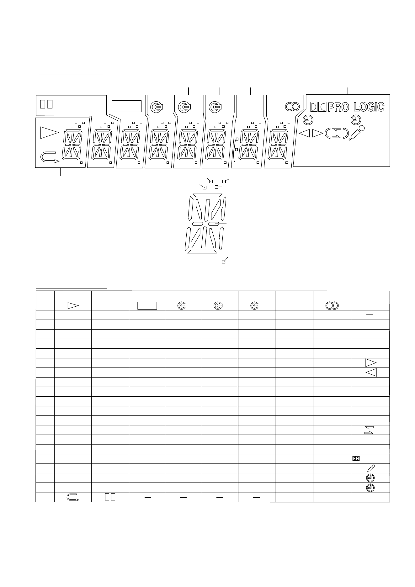
– 47 –
CD-E700H
FL701 VVKNA09SS29-1
FL DISPLAY
X-BASS
X-BASS
MP3
MP3
REC
ST
SLEEP
RDS
EON
kHz
MHz TA MEMORY
TP
TI
PTYIPTY
1
2
3
1 2 3
PTYI
)
(
TA
TP
RDS
MEMORY
TI
PTY
MHz
SLEEP
REC
ST
PRO LOGIC
kHz
EON
a
b
c
d
f
g
m
e
r
p
n
h
j
k
S3
(1G~8G)
S2
S1
S4
Dp
2G
1G
3G 4G 5G 6G
7G
8G 9G
GRID ASSIGNMENT
P1
1G
S1
S2
S3
S4
a
b
k
j
h
f
m
d
g
p
e
n
r
c
Dp
a
b
k
j
h
f
m
d
g
p
e
n
r
c
Dp
a
b
k
j
h
f
m
d
g
p
e
n
r
c
Dp
a
b
k
j
h
f
m
d
g
p
e
n
r
c
Dp
a
b
k
j
h
f
m
d
g
p
e
n
r
c
Dp
a
b
k
j
h
f
m
d
g
p
e
n
r
c
Dp
a
b
k
j
h
f
m
d
g
p
e
n
r
c
Dp
a
b
k
j
h
f
m
d
g
p
e
n
r
c
Dp
S1
S2
S3
S4
S1
S2
S3
S4
S1
S2
S3
S4
S1
S2
S3
S4
S1
S2
S3
S4
S1
S2
S3
S4
S1
S2
S3
S4
2G 3G 4G 5G 6G 7G 8G 9G
P2
P3
P4
P5
P6
P7
P8
P9
P10
P11
P12
P13
P14
P15
P16
P17
P18
P19
P20
P21
col
col
ANODE CONNECTION
(L)
(R)

CD-E700H
– 48 –
–– MEMO ––
CD-E700H
PARTS GUIDE
NOTE:
Parts marked with “ ” are important for maintaining the safety of the set.
Be sure to replace parts with specified ones for maintaining the safety and performance of the set.
“HOW TO ORDER REPLACEMENT PARTS”
To have your order filled promptly and correctly, please furnish the
following information.
1. MODEL NUMBER 2. REF. No.
3. PART NO. 4. DESCRIPTION
MARK: SPARE PARTS-DELIVERY SECTION
For U.S.A. only
Contact your nearest SHARP Parts Distributor to order.
For location of SHARP Parts Distributor,
Please call Toll-Free;
1-800-BE-SHARP
Explanation of capacitors/resistors parts codes
Capacitors
VCC ....................... Ceramic type
VCK........................ Ceramic type
VCT ........................ Semiconductor type
VC • • MF ............... Cylindrical type (without lead wire)
VC • • MN............... Cylindrical type (without lead wire)
VC • • TV ................ Square type (without lead wire)
VC • • TQ ............... Square type (without lead wire)
VC • • CY ............... Square type (without lead wire)
VC • • CZ ............... Square type (without lead wire)
VC • • • • • • • • • J .. The 13th character represents capacity difference.
("J" ±5%, "K" ±10%, "M" ±20%, "N" ±30%,
"C" ±0.25 pF, "D" ±0.5 pF, "Z" +80-20%.)
If there are no indications for the electrolytic capacitors, error is ±20%.
Resistors
VRD ....................... Carbon-film type
VRS........................ Carbon-film type
VRN ....................... Metal-film type
VR • • MF ............... Cylindrical type (without lead wire)
VR • • MN............... Cylindrical type (without lead wire)
VR • • TV ................ Square type (without lead wire)
VR • • TQ ............... Square type (without lead wire)
VR • • CY ............... Square type (without lead wire)
VR • • CZ ............... Square type (without lead wire)
VR • • • • • • • • • J .. The 13th character represents error.
("J" ±5%, "F" ±1%, "D" ±0.5%.)
If there are no indications for other parts, the resistors are ±5%
carbon-film type.
MINI COMPONENT SYSTEM
MODEL CD-E700H
CD-E700H Mini Component System consisting of CD-E700H
(main unit) and CP-E700H (speaker system).

PRICE
RANK
DESCRIPTIONNO. PART CODE NO. PARTS CODE
PRICE
RANK
DESCRIPTION
CD-E700H
INTEGRATED CIRCUITS
IC1 VHILC78646E-1 J AY CD Servo,LC78646E
IC2 VHILA6574H+-1 J AN Focus/Tracking/Spin/Sled Driver,
LA6574H
IC101 VHIAN7345K/-1 J AM Playback and Record/Playback
Amp.,AN7345K
IC302 VHILC72131/-1 J AP PLL (Tuner),LC72131
IC303 VHILA1832S/-1 J AN FM IF Det./FM Mpx./AM IF,
LA1832S
IC601 VHILC75341/-1 J AM Audio Processor,LC75341
IC701 RH-IX0553AWZZ J AX System Microcomputer,
IX0553AW
IC851 VHIKIA7812AP1 J AF Voltage Regulator,KIA7812AP
IC852 VHIKIA7810AP1 J AF Voltage Regulator,KIA7810AP
IC853 VHIKIA7805AP1 J AF Voltage Regulator,KIA7805AP
IC854 VHIAN78L05/-1 J AE Voltage Regulator,AN78L05
IC855 VSKTC2026//-1 J AF Silicon,NPN,KTC2026
IC901 VHISTK41242-1 J BB Power Amp.,STK41242
ICT21 VHILC72723/-1 J AR RDS Decorder,LC72723
TRANSISTORS
Q1 VSKTA1266GR-1 J AB Silicon,PNP,KTA1266 GR
Q4 VSKTA1271Y/-1 J AC Silicon,PNP,KTA1271 Y
Q101~104 VSKTC3200GR-1 J AC Silicon,NPN,KTC3200 GR
Q105~108 VSKTC3199GR-1 J AB Silicon,NPN,KTC3199 GR
Q109 VSKTA1266GR-1 J AB Silicon,PNP,KTA1266 GR
Q110 VSKRC104M//-1 J AC Digital,NPN,KRC104 M
Q111 VSKTC3203Y/-1 J AC Silicon,NPN,KTC3203 Y
Q112 VSKTA1266GR-1 J AB Silicon,PNP,KTA1266 GR
Q113,114 VSKRC104M//-1 J AC Digital,NPN,KRC104 M
Q301 VS2SC380-O/-1 J AC Silicon,NPN,2SC380 O
Q360 VSKTA1266GR-1 J AB Silicon,PNP,KTA1266 GR
Q601~604 VSKTC3199GR-1 J AB Silicon,NPN,KTC3199 GR
Q706~708 VSKTA1273Y/-1 J AE Silicon,PNP,KTA1273 Y
Q709,710 VSKRC102M//-1 J AC Digital,NPN,KRC102 M
Q711 VSKRA107M//-1 J AE Digital,PNP,KRA107 M
Q712 VSKRC104M//-1 J AC Digital,NPN,KRC104 M
Q801 VSKTA1274Y/-1 J AE Silicon,PNP,KTA1274 Y
Q841 VSKTC3199GR-1 J AB Silicon,NPN,KTC3199 GR
Q901~905 VSKTC3199GR-1 J AB Silicon,NPN,KTC3199 GR
Q906 VSKTC3203Y/-1 J AC Silicon,NPN,KTC3203 Y
QT21 VSKTC3199GR-1 J AB Silicon,NPN,KTC3199 GR
DIODES
D301,302 VHDDS1SS133-1 J AB Silicon,DS1SS133
D701 VHDDS1SS133-1 J AB Silicon,DS1SS133
D704 VHDDS1SS133-1 J AB Silicon,DS1SS133
D709~715 VHDDS1SS133-1 J AB Silicon,DS1SS133
D716 VHDDS1SS133-1 J AB Silicon,DS1SS133
D801,802 VHDD10XB60F-1 J AL Silicon,D10XB60F
D803~806 VHD1N4004S/-1 J AB Silicon,1N4004S
D842~845 VHD1N4004S/-1 J AB Silicon,1N4004S
1 D846 VHDDS1SS133-1 J AB Silicon,DS1SS133
D851,852 VHDDS1SS133-1 J AB Silicon,DS1SS133
D853 VHD1N4004S/-1 J AB Silicon,1N4004S
D855 VHDDS1SS133-1 J AB Silicon,DS1SS133
D856 VHDDS1SS133-1 J AB Silicon,DS1SS133
D857~859 VHDDS1SS133-1 J AB Silicon,DS1SS133
D905~907 VHDDS1SS133-1 J AB Silicon,DS1SS133
D909,910 VHD1N4004S/-1 J AB Silicon,1N4004S
D911,912 VHDDS1SS133-1 J AB Silicon,DS1SS133
LED701 VHP304VT2E1-1 J AC LED,Red,304VT2E1
LED703,704 VHPA503BC2E-1 J AN LED,White,A503BC2E
ZD1 VHEDZ3R3BSB-1 J AB Zener,3.3V,DZ3.3BSB
ZD351 VHEDZ5R1BSB-1 J AC Zener,5.1V,DZ5.1BSB
ZD801,802 VHEDZ6R2BSA-1 J AB Zener,6.2V,DZ6.2BSA
ZD803 VHEDZ300BSB-1 J AB Zener,30V,DZ30BSB
ZD852 VHEDZ8R2BSB-1 J AB Zener,8.2V,DZ8.2B
ZD902,903 VHEDZ120BSB-1 J AB Zener,12V,DZ12BSB
ZDT21 VHEDZ5R1BSB-1 J AC Zener,5.1V,DZ5.1BSB
FILTERS
CF301,302 RFILF0072AFZZ J AG FM IF
CF351 RFILF0003AWZZ J AK FM IF
CF352 RFILA0009AWZZ J AE AM IF
TRANSFORMERS
1 PT801 RTRNP0468AWZZ J BE Power,Main
1 PT841 RTRNP0313AWZZ J AN Power,Sub
T303 RCILA0052AWZZ J AE AM Tracking
T306 RCILB0067AWZZ J AD OSC.,AM
T351 RCILI0019AWZZ J AD AM IF
COILS
L1 VP-XHR82K0000 J AC 0.82 µH,Choke
L103 VP-MK331K0000 J AB 330 µH,Choke
L341 RBLN-0002AWZZ J AE Balum
L342 VP-DH2R2K0000 J AB 2.2 µH,Peaking
L351,352 VP-DH101K0000 J AB 100 µH,Choke
L354 RFILL0001AWZZ J AE Low Pass Filter
L701 VP-DH101K0000 J AB 100 µH,Choke
L702 VP-DH2R2K0000 J AB 2.2 µH,Peaking
1 L841 RCILZ0022AWZZ J AG Line Filter
L901,902 RCILZ0024AWZZ J AC 3 µH,Choke
L920,921 RCILZ0137AFZZ J AA 0.29 µH
LT21,22 VP-XH2R2K0000 J AB 2.2 µH,Choke
VARIABLE CAPACITOR
VD301 VHCSVC348S/-1 J AK Variable Capacitance,SVC348S
VIBRATORS
X351 92LCRSTL1425A J AF Crystal,456 kHz
X352 RCRSP0019AWZZ J AF Crystal,4.5 MHz
XL1 RCRM-0047AWZZ J AE Ceramic,16.9344 MHz
XL701 RCRSP0003AWZZ J AH Crystal,4.194304 MHz
XT21 RCRSP0018AWZZ J AG Crystal,4.332 MHz
CAPACITORS
C1 VCEAZA1EW476M J AB 47 µF,25V,Electrolytic
C2 VCTYMN1CY103N J AA 0.01 µF,16V
C3 VCEAZA1EW476M J AB 47 µF,25V,Electrolytic
C4 VCKYMN1HB102K J AA 0.001 µF,50V
C5 VCQYKA1HM473J J AB 0.047 µF,50V,Mylar
C6 VCTYPA1CX104K J AB 0.1 µF,16V
C8 VCTYMN1CX272K J AA 0.0027 µF,16V
C9 RC-EZ0004AWZZ J AD 3.3 µF,16V,Electrolytic
C10 RC-EZY106AF1E J AB 10 µF,25V,Electrolytic
C11 RC-EZY224AF1H J AB 0.22 µF,50V,Electrolytic
C12 VCKYMN1HB101K J AA 100 pF,50V
C13 VCTYMN1EF223Z J AA 0.022 µF,25V
C14 RC-EZY107AF1A J AB 100 µF,10V,Electrolytic
C15 VCKYMN1HB102K J AA 0.001 µF,50V
C16 RC-EZY337AF0J J AA 330 µF,6.3V,Electrolytic
C17 VCEAZA1AW107M J AB 100 µF,10V,Electrolytic
C19 VCTYMN1EF223Z J AA 0.022 µF,25V
C20,21 VCKYMN1HB102K J AA 0.001 µF,50V
C22 VCTYMN1CY103N J AA 0.01 µF,16V
C23,24 RC-EZY106AF1E J AB 10 µF,25V,Electrolytic
C25,26 VCQYKA1HM152K J AB 0.0015 µF,50V,Mylar
C27 VCTYMN1EF223Z J AA 0.022 µF,25V
C28~30 VCKYMN1HB101K J AA 100 pF,50V
C33 VCKYMN1HB101K J AA 100 pF,50V
C35 VCQYKA1HM473J J AB 0.047 µF,50V,Mylar
C36 VCEAZA1HW224M J AB 0.22 µF,50V,Electrolytic
C37 VCTYPA1CX104K J AB 0.1 µF,16V
C38 VCTYMN1CY103N J AA 0.01 µF,16V
C39~41 VCEAZA1AW107M J AB 100 µF,10V,Electrolytic
C42 VCTYMN1CY103N J AA 0.01 µF,16V
C43 VCTYMN1EF223Z J AA 0.022 µF,25V
C44 VCKYMN1HB102K J AA 0.001 µF,50V
C45 VCCCMN1HH220J J AA 22 pF (CH),50V
C48 VCKYMN1HB102K J AA 0.001 µF,50V
C101,102 VCKYMN1HB561K J AA 560 pF,50V
C103 VCKYBT1HB181K J AA 180 pF,50V
C104 VCKYMN1HB181K J AA 180 pF,50V
C105,106 VCKYMN1HB561K J AA 560 pF,50V
C107~110 VCKYMN1HB331K J AA 330 pF,50V
– 1 –
CD-E700H

NO.
PRICE
RANK
DESCRIPTION
PARTS CODENO. PART CODE
PRICE
RANK
DESCRIPTION
CD-E700H
C111,112 VCEAZA1EW476M J AB 47 µF,25V,Electrolytic
C113,114 VCTYPA1EX333K J AA 0.033 µF,25V
C115,116 VCKYMN1HB561K J AA 560 pF,50V
C117,118 VCEAZA1EW476M J AB 47 µF,25V,Electrolytic
C119,120 VCTYMN1CX222K J AA 0.0022 µF,16V
C121 VCTYMN1EF223Z J AA 0.022 µF,25V
C123,124 VCKYMN1HB271K J AA 270 pF,50V
C125,126 VCEAZA1HW226M J AB 22 µF,50V,Electrolytic
C127,128 VCTYPA1CX223K J AA 0.022 µF,16V
C129,130 VCTYMN1CX332K J AA 0.0033 µF,16V
C131,132 VCEAZA1EW476M J AB 47 µF,25V,Electrolytic
C133 VCEAZA1HW226M J AB 22 µF,50V,Electrolytic
C134 VCEAZA1AW227M J AC 220 µF,10V,Electrolytic
C135 VCTYMN1EF223Z J AA 0.022 µF,25V
C137 VCQYKA1HM473K J AB 0.047 µF,50V,Mylar
C138 VCQPKA2AA822J J AA 0.0082 µF,100V,Polypropylene
C139 VCQYKA1HM393K J AB 0.039 µF,50V,Mylar
C140 VCEAZA1EW476M J AB 47 µF,25V,Electrolytic
C141 VCEAZA1CW107M J AC 100 µF,16V,Electrolytic
C143 VCEAZA1HW335M J AB 3.3 µF,50V,Electrolytic
C150 VCEAZA1HW476M J AB 47 µF,50V,Electrolytic
C321 VCEAZA1CW107M J AC 100 µF,16V,Electrolytic
C323 VCTYMN1EF223Z J AA 0.022 µF,25V
C330 VCCUMN1HJ150J J AA 15 pF (UJ),50V
C331 VCKZPA1HF473Z J AA 0.047 µF,50V
C332 VCTYMN1EF223Z J AA 0.022 µF,25V
C334 VCCCMN1HH220J J AA 22 pF (CH),50V
C335 VCKYMN1HB561K J AA 560 pF,50V
C338 VCKYMN1HB102K J AA 0.001 µF,50V
C341,342 VCTYMN1EF223Z J AA 0.022 µF,25V
C345~347 VCTYMN1EF223Z J AA 0.022 µF,25V
C348 VCTYMN1EF103Z J AB 0.01 µF,25V
C350,351 VCTYMN1EF223Z J AA 0.022 µF,25V
C352 VCEAZA1HW106M J AB 10 µF,50V,Electrolytic
C353,354 VCTYMN1EF223Z J AA 0.022 µF,25V
C355 VCCSMN1HL220J J AA 22 pF,50V
C356 VCKYMN1HB102K J AA 0.001 µF,50V
C357 VCEAZA1HW225M J AB 2.2 µF,50V,Electrolytic
C358 VCEAZA1HW105M J AB 1 µF,50V,Electrolytic
C361 VCTYMN1EF223Z J AA 0.022 µF,25V
C362 VCEAZA1HW335M J AB 3.3 µF,50V,Electrolytic
C363 VCTYMN1EF223Z J AA 0.022 µF,25V
C364 VCEAZA1HW225M J AB 2.2 µF,50V,Electrolytic
C365 VCKZPA1HF223Z J AA 0.022 µF,50V
C366 VCKYMN1HB102K J AA 0.001 µF,50V
C367,368 VCEAZA1HW105M J AB 1 µF,50V,Electrolytic
C369 VCCUMN1HJ270J J AA 27 pF (UJ),50V
C370~372 VCEAZA1HW105M J AB 1 µF,50V,Electrolytic
C373,374 VCTYPA1CX153K J AA 0.015 µF,16V
C380 VCEAZA1HW106M J AB 10 µF,50V,Electrolytic
C381 VCCCMN1HH120J J AA 12 pF (CH),50V
C382 VCCCMN1HH150J J AA 15 pF (CH),50V
C383 VCCSBT1HL470J J AA 47 pF,50V
C384 VCKYMN1HB102K J AA 0.001 µF,50V
C385 VCTYMN1CY103N J AA 0.01 µF,16V
C386 VCKYMN1HB331K J AA 330 pF,50V
C387 VCTYMN1EF223Z J AA 0.022 µF,25V
C388 VCKYMN1HB102K J AA 0.001 µF,50V
C389 VCKYBT1HB102K J AA 0.001 µF,50V
C391 VCEAZA1EW476M J AB 47 µF,25V,Electrolytic
C392 VCKYMN1HB102K J AA 0.001 µF,50V
C393 VCEAZA1HW105M J AB 1 µF,50V,Electrolytic
C394 VCEAZA1EW476M J AB 47 µF,25V,Electrolytic
C395 VCTYMN1EF223Z J AA 0.022 µF,25V
C396 VCEAZA1AW107M J AB 100 µF,10V,Electrolytic
C397 VCTYMN1EF223Z J AA 0.022 µF,25V
C398 VCEAZA1AW107M J AB 100 µF,10V,Electrolytic
C399 VCTYMN1EF223Z J AA 0.022 µF,25V
C601 VCEAZA1CW227M J AC 220 µF,16V,Electrolytic
C602 VCKZPA1HF223Z J AA 0.022 µF,50V
C603 VCEAZA1HW226M J AB 22 µF,50V,Electrolytic
C605,606 VCFYHA1HA124J J AB 0.12 µF,50V,Thin Film
C607,608 VCFYHA1HA154J J AC 0.15 µF,50V,Thin Film
C609,610 VCEAZA1HW105M J AB 1 µF,50V,Electrolytic
C611,612 VCTYMN1CX222K J AA 0.0022 µF,16V
C613,614 VCEAZA1HW105M J AB 1 µF,50V,Electrolytic
C615,616 VCEAZA1HW475M J AB 4.7 µF,50V,Electrolytic
C617~624 VCEAZA1HW105M J AB 1 µF,50V,Electrolytic
C625,626 VCTYMN1CX222K J AA 0.0022 µF,16V
C639 VCEAZA1HW105M J AB 1 µF,50V,Electrolytic
C640 VCEAZA1HW226M J AB 22 µF,50V,Electrolytic
C651~653 VCKYMN1HB221K J AA 220 pF,50V
C690,691 VCKYMN1HB391K J AA 390 pF,50V
C701 VCEAZA1HW105M J AB 1 µF,50V,Electrolytic
C702 VCEAZA1AW227M J AC 220 µF,10V,Electrolytic
C704 VCCSMN1HL150J J AA 15 pF,50V
C705 VCCSMN1HL180J J AA 18 pF,50V
C707 VCEAZA1HW105M J AB 1 µF,50V,Electrolytic
C709,710 VCTYMN1CX472K J AA 0.0047 µF,16V
C712 VCEAZA1EW476M J AB 47 µF,25V,Electrolytic
C714 VCEAZA1HW335M J AB 3.3 µF,50V,Electrolytic
C715 VCTYMN1EF103Z J AB 0.01 µF,25V
C717 VCEAZA1EW476M J AB 47 µF,25V,Electrolytic
C718,719 VCKYMN1HB101K J AA 100 pF,50V
C720,721 VCTYMN1EF223Z J AA 0.022 µF,25V
C801 VCEAZA1VW107M J AC 100 µF,35V,Electrolytic
C802,803 VCEAZA1HW476M J AB 47 µF,50V,Electrolytic
C804 VCEAZA1JW227M J AD 220 µF,63V,Electrolytic
C805 VCEAZA2AW226M J AC 22 µF,100V,Electrolytic
C806~809 VCQYKA1HM104K J AB 0.1 µF,50V,Mylar
C810,811 VCQYKU2AM224K J AB 0.22 µF,100V,Mylar
C841 VCEAZA0JW108M J AC 1000 µF,6.3V,Electrolytic
C842 VCEAZA1VW477M J AD 470 µF,35V,Electrolytic
C843 VCQYKA1HM473K J AB 0.047 µF,50V,Mylar
1 C844 RC-KZ002LAWZZ J AC 0.047 µF,250V,Ceramic
C851 VCQYKA1HM104K J AB 0.1 µF,50V,Mylar
C854,855 VCQYKA1HM104K J AB 0.1 µF,50V,Mylar
C856 VCEAZW1VW338M J AH 3300 µF,35V,Electrolytic
C858,859 VCQYKA1HM104K J AB 0.1 µF,50V,Mylar
C861 VCKZPA1HF223Z J AA 0.022 µF,50V
C863 VCEAZA1HW226M J AB 22 µF,50V,Electrolytic
C864 VCQYKA1HM104K J AB 0.1 µF,50V,Mylar
C865 VCEAZA1HW106M J AB 10 µF,50V,Electrolytic
C901,902 VCEAZA1HW104M J AB 0.1 µF,50V,Electrolytic
C903,904 VCKYMN1HB102K J AA 0.001 µF,50V
C905,906 VCEAZA1HW226M J AB 22 µF,50V,Electrolytic
C907 VCKYMN1HB101K J AA 100 pF,50V
C908 VCCCMN1HH3R3C J AA 3.3 pF (CH),50V
C909 VCQYKA1HM104K J AB 0.1 µF,50V,Mylar
C910 VCCCMN1HH3R3C J AA 3.3 pF (CH),50V
C911,912 VCEAZA2AW107M J AD 100 µF,100V,Electrolytic
C913 VCKYMN1HB101K J AA 100 pF,50V
C914,915 VCEAZA2AW107M J AD 100 µF,100V,Electrolytic
C916 VCEAZA1HW107M J AC 100 µF,50V,Electrolytic
C917 VCQYKA1HM103K J AA 0.01 µF,50V,Mylar
C918 VCEAZA1HW107M J AC 100 µF,50V,Electrolytic
C919 VCQYKA1HM103K J AA 0.01 µF,50V,Mylar
C920 RC-EZ0029AWZZ J AN 3300 µF,71V,Electrolytic
C921,922 RC-EZ0106AWZZ J AH 4700 µF,35V,Electrolytic
C923 RC-EZ0029AWZZ J AN 3300 µF,71V,Electrolytic
C925 VCEAZA1HW476M J AB 47 µF,50V,Electrolytic
C926~929 VCFYHA1HA224J J AC 0.22 µF,50V,Thin Film
C931 VCEAZA1HW106M J AB 10 µF,50V,Electrolytic
C934~941 VCKZPA1HF223Z J AA 0.022 µF,50V
C942,943 VCKYPA1HB102K J AA 0.001 µF,50V
C946 VCEAZA1HW104M J AB 0.1 µF,50V,Electrolytic
CT21 VCEAZA1EW476M J AB 47 µF,25V,Electrolytic
CT22 VCTYMN1EF223Z J AA 0.022 µF,25V
CT23 VCCCMN1HH220J J AA 22 pF (CH),50V
CT24 VCEAZA1EW476M J AB 47 µF,25V,Electrolytic
CT25 VCCCMN1HH220J J AA 22 pF (CH),50V
CT26 VCKYMN1HB561K J AA 560 pF,50V
CT27~30 VCTYMN1EF223Z J AA 0.022 µF,25V
CT31,32 VCEAZA1EW476M J AB 47 µF,25V,Electrolytic
RESISTORS
VRD-MN2BD000C J AA 0 ohm,Jumper,ø1.4×3.5mm,Ivory
R1,2 VRD-MN2BD822J J AA 8.2 kohms,1/8W
R3 VRD-MN2BD223J J AA 22 kohms,1/8W
R4,5 VRD-MN2BD822J J AA 8.2 kohms,1/8W
R6 VRD-MN2BD223J J AA 22 kohms,1/8W
R7 VRD-ST2CD470J J AA 47 ohms,1/6W
R8 VRD-ST2CD103J J AA 10 kohm,1/6W
R9 VRD-MN2BD100J J AA 10 ohm,1/8W
R10 VRD-MN2BD273J J AA 27 kohms,1/8W
R11 VRD-MN2BD103J J AA 10 kohm,1/8W
R12 VRD-MN2BD331J J AA 330 ohms,1/8W
R13 VRD-ST2CD153J J AA 15 kohms,1/6W
R14,15 VRD-MN2BD102J J AA 1 kohm,1/8W
R16 VRD-ST2CD102J J AA 1 kohm,1/6W
R18 VRD-MN2BD102J J AA 1 kohm,1/8W
R19 VRD-ST2CD153J J AA 15 kohms,1/6W
– 2 –

PRICE
RANK
DESCRIPTIONNO. PART CODE NO. PARTS CODE
PRICE
RANK
DESCRIPTION
CD-E700H
R20 VRD-MN2BD103J J AA 10 kohm,1/8W
R21 VRD-ST2EE1R0J J AA 1 ohm,1/4W
R22 VRD-ST2CD101J J AA 100 ohm,1/6W
R24,25 VRD-MN2BD222J J AA 2.2 kohms,1/8W
R26,27 VRD-MN2BD103J J AA 10 kohm,1/8W
R28,29 VRD-ST2CD222J J AA 2.2 kohms,1/6W
R31 VRD-ST2CD472J J AA 4.7 kohms,1/6W
R32~38 VRD-ST2CD102J J AA 1 kohm,1/6W
R39,40 VRD-MN2BD681J J AA 680 ohms,1/8W
R41 VRD-MN2BD123J J AA 12 kohms,1/8W
R42 VRD-MN2BD122J J AA 1.2 kohms,1/8W
R43 VRD-MN2BD221J J AA 220 ohms,1/8W
R46 VRD-ST2EE1R0J J AA 1 ohm,1/4W
R101,102 VRD-MN2BD102J J AA 1 kohm,1/8W
R103,104 VRD-MN2BD222J J AA 2.2 kohms,1/8W
R105,106 VRD-MN2BD332J J AA 3.3 kohms,1/8W
R107,108 VRD-MN2BD473J J AA 47 kohms,1/8W
R109,110 VRD-MN2BD472J J AA 4.7 kohms,1/8W
R111 VRD-ST2CD153J J AA 15 kohms,1/6W
R112 VRD-MN2BD153J J AA 15 kohms,1/8W
R113,114 VRD-ST2CD102J J AA 1 kohm,1/6W
R115,116 VRD-ST2CD560J J AA 56 ohms,1/6W
R117,118 VRD-MN2BD104J J AA 100 kohm,1/8W
R119,120 VRD-MN2BD392J J AA 3.9 kohms,1/8W
R121,122 VRD-MN2BD123J J AA 12 kohms,1/8W
R123,124 VRD-MN2BD562J J AA 5.6 kohms,1/8W
R126,127 VRD-MN2BD472J J AA 4.7 kohms,1/8W
R128,129 VRD-MN2BD562J J AA 5.6 kohms,1/8W
R130,131 VRD-MN2BD152J J AA 1.5 kohms,1/8W
R132,133 VRD-MN2BD101J J AA 100 ohm,1/8W
R134,135 VRD-MN2BD103J J AA 10 kohm,1/8W
R136 VRD-ST2CD224J J AA 220 kohms,1/6W
R137 VRD-MN2BD224J J AA 220 kohms,1/8W
R138 VRD-ST2CD103J J AA 10 kohm,1/6W
R139 VRD-MN2BD103J J AA 10 kohm,1/8W
R140 VRD-MN2BD473J J AA 47 kohms,1/8W
R141 VRD-ST2CD472J J AA 4.7 kohms,1/6W
R142 VRD-RT2HD820J J AA 82 ohms,1/2W
R143 VRD-MN2BD473J J AA 47 kohms,1/8W
R144 VRD-MN2BD223J J AA 22 kohms,1/8W
R145 VRD-ST2CD4R7J J AA 4.7 ohms,1/6W
R146,147 VRD-MN2BD103J J AA 10 kohm,1/8W
R148 VRD-MN2BD472J J AA 4.7 kohms,1/8W
R149 VRD-ST2EE151J J AA 150 ohms,1/4W
R150 VRD-MN2BD683J J AA 68 kohms,1/8W
R158 VRD-ST2EE221J J AA 220 ohms,1/4W
R323 VRD-MN2BD683J J AA 68 kohms,1/8W
R336 VRD-MN2BD103J J AA 10 kohm,1/8W
R344 VRD-MN2BD471J J AA 470 ohms,1/8W
R345 VRD-MN2BD472J J AA 4.7 kohms,1/8W
R346 VRD-MN2BD331J J AA 330 ohms,1/8W
R347 VRD-MN2BD682J J AA 6.8 kohms,1/8W
R348 VRD-MN2BD681J J AA 680 ohms,1/8W
R349 VRD-MN2BD330J J AA 33 ohms,1/8W
R350 VRD-MN2BD272J J AA 2.7 kohms,1/8W
R351 VRD-MN2BD562J J AA 5.6 kohms,1/8W
R352 VRD-MN2BD102J J AA 1 kohm,1/8W
R353 VRD-MN2BD271J J AA 270 ohms,1/8W
R355 VRD-MN2BD332J J AA 3.3 kohms,1/8W
R356 VRD-MN2BD102J J AA 1 kohm,1/8W
R357 VRD-ST2CD474J J AA 470 kohms,1/6W
R358 VRD-ST2CD392J J AA 3.9 kohms,1/6W
R359 VRD-MN2BD182J J AA 1.8 kohms,1/8W
R360 VRD-MN2BD472J J AA 4.7 kohms,1/8W
R365 VRD-MN2BD103J J AA 10 kohm,1/8W
R369 VRD-MN2BD150J J AA 15 ohms,1/8W
R370 VRD-ST2CD102J J AA 1 kohm,1/6W
R372~374 VRD-MN2BD102J J AA 1 kohm,1/8W
R376 VRD-MN2BD102J J AA 1 kohm,1/8W
R377 VRD-MN2BD473J J AA 47 kohms,1/8W
R378 VRD-MN2BD102J J AA 1 kohm,1/8W
R379 VRD-MN2BD222J J AA 2.2 kohms,1/8W
R380 VRD-MN2BD152J J AA 1.5 kohms,1/8W
R381 VRD-MN2BD103J J AA 10 kohm,1/8W
R382 VRD-ST2EE151J J AA 150 ohms,1/4W
R383 VRD-MN2BD562J J AA 5.6 kohms,1/8W
R384 VRD-ST2CD562J J AA 5.6 kohms,1/6W
R385 VRD-MN2BD562J J AA 5.6 kohms,1/8W
R386 VRD-ST2CD223J J AA 22 kohms,1/6W
R387 VRD-ST2CD562J J AA 5.6 kohms,1/6W
R388 VRD-MN2BD392J J AA 3.9 kohms,1/8W
R391,392 VRD-ST2EE271J J AA 270 ohms,1/4W
R393 VRD-MN2BD102J J AA 1 kohm,1/8W
R395 VRD-MN2BD473J J AA 47 kohms,1/8W
R399 VRD-MN2BD330J J AA 33 ohms,1/8W
R601~603 VRD-ST2CD102J J AA 1 kohm,1/6W
R604 VRD-ST2CD103J J AA 10 kohm,1/6W
R605 VRD-MN2BD103J J AA 10 kohm,1/8W
R606,607 VRD-MN2BD392J J AA 3.9 kohms,1/8W
R608,609 VRD-MN2BD122J J AA 1.2 kohms,1/8W
R610,611 VRD-MN2BD222J J AA 2.2 kohms,1/8W
R612,613 VRD-MN2BD391J J AA 390 ohms,1/8W
R614,615 VRD-MN2BD332J J AA 3.3 kohms,1/8W
R616,617 VRD-MN2BD222J J AA 2.2 kohms,1/8W
R618 VRD-ST2CD331J J AA 330 ohms,1/6W
R619 VRD-MN2BD331J J AA 330 ohms,1/8W
R620,621 VRD-MN2BD223J J AA 22 kohms,1/8W
R641 VRD-MN2BD103J J AA 10 kohm,1/8W
R642 VRD-ST2CD103J J AA 10 kohm,1/6W
R643,644 VRD-MN2BD223J J AA 22 kohms,1/8W
R690,691 VRD-MN2BD682J J AA 6.8 kohms,1/8W
R692,693 VRD-MN2BD333J J AA 33 kohms,1/8W
R702 VRD-MN2BD102J J AA 1 kohm,1/8W
R703,704 VRD-ST2CD102J J AA 1 kohm,1/6W
R705 VRD-MN2BD102J J AA 1 kohm,1/8W
R706 VRD-ST2CD102J J AA 1 kohm,1/6W
R708~716 VRD-MN2BD102J J AA 1 kohm,1/8W
R717 VRD-ST2CD101J J AA 100 ohm,1/6W
R718~720 VRD-MN2BD102J J AA 1 kohm,1/8W
R721 VRD-ST2CD102J J AA 1 kohm,1/6W
R722 VRD-MN2BD102J J AA 1 kohm,1/8W
R724 VRD-MN2BD102J J AA 1 kohm,1/8W
R725 VRD-ST2CD102J J AA 1 kohm,1/6W
R726,727 VRD-ST2CD681J J AA 680 ohms,1/6W
R728 VRD-ST2CD222J J AA 2.2 kohms,1/6W
R729 VRD-MN2BD561J J AA 560 ohms,1/8W
R730 VRD-MN2BD102J J AA 1 kohm,1/8W
R731 VRD-MN2BD103J J AA 10 kohm,1/8W
R732 VRD-MN2BD102J J AA 1 kohm,1/8W
R733 VRD-ST2CD102J J AA 1 kohm,1/6W
R734~736 VRD-MN2BD102J J AA 1 kohm,1/8W
R737 VRD-ST2CD101J J AA 100 ohm,1/6W
R739 VRD-ST2CD102J J AA 1 kohm,1/6W
R740 VRD-ST2CD472J J AA 4.7 kohms,1/6W
R742~745 VRD-ST2CD102J J AA 1 kohm,1/6W
R746 VRD-MN2BD102J J AA 1 kohm,1/8W
R747 VRD-MN2BD472J J AA 4.7 kohms,1/8W
R749 VRD-MN2BD331J J AA 330 ohms,1/8W
R750 VRD-ST2CD473J J AA 47 kohms,1/6W
R751 VRD-MN2BD331J J AA 330 ohms,1/8W
R756 VRD-MN2BD472J J AA 4.7 kohms,1/8W
R757,758 VRD-MN2BD102J J AA 1 kohm,1/8W
R759 VRD-ST2CD562J J AA 5.6 kohms,1/6W
R761 VRD-MN2BD103J J AA 10 kohm,1/8W
R762 VRD-ST2CD103J J AA 10 kohm,1/6W
R763,764 VRD-MN2BD102J J AA 1 kohm,1/8W
R765 VRD-ST2CD472J J AA 4.7 kohms,1/6W
R766~768 VRD-MN2BD103J J AA 10 kohm,1/8W
R769 VRD-MN2BD102J J AA 1 kohm,1/8W
R770 VRD-MN2BD103J J AA 10 kohm,1/8W
R772,773 VRD-MN2BD103J J AA 10 kohm,1/8W
R775~780 VRD-MN2BD103J J AA 10 kohm,1/8W
R781 VRD-MN2BD473J J AA 47 kohms,1/8W
R782 VRD-MN2BD104J J AA 100 kohm,1/8W
R783 VRD-ST2CD101J J AA 100 ohm,1/6W
R788,789 VRD-ST2CD103J J AA 10 kohm,1/6W
R791 VRD-MN2BD472J J AA 4.7 kohms,1/8W
R794,795 VRD-ST2EE1R5J J AA 1.5 ohms,1/4W
R801 VRD-ST2CD104J J AA 100 kohm,1/6W
R802 VRD-ST2CD473J J AA 47 kohms,1/6W
R803 VRD-ST2CD123J J AA 12 kohms,1/6W
R804,805 VRD-ST2EE470J J AA 47 ohms,1/4W
R806 VRD-ST2CD473J J AA 47 kohms,1/6W
R808 VRD-RT2HD222J J AA 2.2 kohms,1/2W
R841 VRD-ST2CD224J J AA 220 kohms,1/6W
R842 VRD-ST2CD102J J AA 1 kohm,1/6W
R843 VRD-ST2CD473J J AA 47 kohms,1/6W
R844 VRD-ST2EE820J J AA 82 ohms,1/4W
R852 VRD-ST2CD103J J AA 10 kohm,1/6W
R853,854 VRD-ST2CD223J J AA 22 kohms,1/6W
R858 VRD-ST2CD221J J AA 220 ohms,1/6W
R859 VRD-ST2CD223J J AA 22 kohms,1/6W
R860 VRD-ST2EE221J J AA 220 ohms,1/4W
R901,902 VRD-MN2BD563J J AA 56 kohms,1/8W
– 3 –

NO.
PRICE
RANK
DESCRIPTION
PARTS CODENO. PART CODE
PRICE
RANK
DESCRIPTION
CD-E700H
R903,904 VRD-MN2BD102J J AA 1 kohm,1/8W
R905,906 VRD-MN2BD561J J AA 560 ohms,1/8W
R907 VRD-MN2BD563J J AA 56 kohms,1/8W
R908 VRD-MN2BD102J J AA 1 kohm,1/8W
R909 VRD-MN2BD333J J AA 33 kohms,1/8W
R910 VRD-MN2BD102J J AA 1 kohm,1/8W
R911 VRD-ST2CD563J J AA 56 kohms,1/6W
1 R912 VRG-ST2EC101J J AB 100 ohm,1/4W,Fusible
R913 VRN-VV3LAR22J J AC 0.22 ohms,3W
R916 VRN-VV3LAR22J J AC 0.22 ohms,3W
R917 VRN-VV3LAR10J J AD 0.1 ohm,3W
R918 VRD-ST2CD152J J AA 1.5 kohms,1/6W
R919,920 VRD-ST2CD182J J AA 1.8 kohms,1/6W
R921 VRD-ST2CD152J J AA 1.5 kohms,1/6W
R922 VRN-VV3LAR10J J AD 0.1 ohm,3W
R925,926 VRD-RT2HD152J J AA 1.5 kohms,1/2W
R927,928 VRD-ST2EE393J J AA 39 kohms,1/4W
R929,930 VRD-ST2EE473J J AA 47 kohms,1/4W
R934,935 VRD-ST2CD563J J AA 56 kohms,1/6W
R937 VRD-ST2CD563J J AA 56 kohms,1/6W
R938~941 VRD-RT2HD100J J AA 10 ohm,1/2W
R942,943 VRS-VV3DA391J J AC 390 ohms,2W
R944,945 VRD-ST2CD152J J AA 1.5 kohms,1/6W
R946 VRD-ST2CD473J J AA 47 kohms,1/6W
R947 VRD-ST2CD153J J AA 15 kohms,1/6W
R949 VRD-ST2CD102J J AA 1 kohm,1/6W
R950 VRD-ST2CD683J J AA 68 kohms,1/6W
R952~955 VRD-ST2EE6R8J J AA 6.8 ohms,1/4W
1 R958 VRG-ST2EC101J J AB 100 ohm,1/4W,Fusible
R961 VRD-MN2BD1R0J J AA 1 ohm,1/8W
RD01 VRD-ST2CD681J J AA 680 ohms,1/6W
RD02 VRD-MN2BD821J J AA 820 ohms,1/8W
RD03 VRD-MN2BD102J J AA 1 kohm,1/8W
RD04 VRD-MN2BD152J J AA 1.5 kohms,1/8W
RD05 VRD-MN2BD222J J AA 2.2 kohms,1/8W
RD06 VRD-MN2BD272J J AA 2.7 kohms,1/8W
RD07 VRD-ST2CD392J J AA 3.9 kohms,1/6W
RD08 VRD-MN2BD562J J AA 5.6 kohms,1/8W
RD09 VRD-MN2BD103J J AA 10 kohm,1/8W
RD10 VRD-MN2BD681J J AA 680 ohms,1/8W
RD11 VRD-MN2BD821J J AA 820 ohms,1/8W
RD12 VRD-MN2BD102J J AA 1 kohm,1/8W
RD13 VRD-ST2CD152J J AA 1.5 kohms,1/6W
RD14 VRD-MN2BD222J J AA 2.2 kohms,1/8W
RD15 VRD-MN2BD272J J AA 2.7 kohms,1/8W
RD16 VRD-MN2BD392J J AA 3.9 kohms,1/8W
RD19 VRD-MN2BD681J J AA 680 ohms,1/8W
RD20 VRD-ST2CD821J J AA 820 ohms,1/6W
RD21 VRD-MN2BD102J J AA 1 kohm,1/8W
RT21 VRD-MN2BD103J J AA 10 kohm,1/8W
RT22,23 VRD-ST2EE391J J AA 390 ohms,1/4W
RT24 VRD-MN2BD563J J AA 56 kohms,1/8W
RT25 VRD-MN2BD103J J AA 10 kohm,1/8W]
RT26 VRD-MN2BD563J J AA 56 kohms,1/8W
RT27~30 VRD-MN2BD102J J AA 1 kohm,1/8W
RT31 VRD-MN2BD103J J AA 10 kohm,1/8W
RT32 VRD-MN2BD682J J AA 6.8 kohms,1/8W
OTHER CIRCUITRY PARTS
BI4/CNS4 QCNWN1572AWZZ J AF Connector Ass’y,6/6Pin
BI601/CNS601 QCNWN2465AWZZ J AG Connector Ass’y,9/8Pin
BI701/CNS701 QCNWN2466AWZZ J AH Connector Ass’y,11/10Pin
BI703/CNS703 QCNWN2505AWZZ J AC Connector Ass’y,2/2Pin
BI704/CNS704 QCNWN2505AWZZ J AC Connector Ass’y,2/2Pin
BI801/CNS801 QCNWN2572AWZZ J Connector Ass’y,11/10Pin
CNP1 QCNCM704GAWZZ J AC Plug,7Pin
CNP2 QCNCM704HAWZZ J AC Plug,8Pin
CNP3 92LCONE6P53253 J AC Plug,6Pin
CNP3A 92LCONE6P53254 J AC Plug,6Pin
CNP4 QCNCM705FAFZZ J AB Plug,6Pin
CNP5 92LCONE8P53254 J AC Plug,8Pin
CNP6 92LCONEAP53254 J AD Plug,10Pin
CNP101 QCNCM705CAFZZ J AA Plug,3Pin
CNP102 QCNCM705GAFZZ J AB Plug,7Pin
CNP302 92LCONE2P5268 J AB Plug,2Pin
CNP701A QCNCWZY24AWZZ J AD Socket,24Pin
CNP701B QCNCWZX24AWZZ J AD Socket,24Pin
CNP702 QCNCWZY07AWZZ J AC Socket,7Pin
CNP703,704 92LCONE2P53253 J AB Plug,2Pin
CNP705 QCNCW012EAWZZ J AC Socket,5Pin
CNP801 92LCONEAP5267X J AC Plug,10Pin
CNP802 QCNCW012FAWZZ J AC Plug,6Pin
CNP805 QCNCM049BAWZZ J AC Plug,2Pin
CNP971 92LCONE2P53253 J AB Plug,2Pin
CNS1A/B QCNWN1537AWZZ J AG Connector Ass’y,7/7Pin
CNS2A/B QCNWN1538AWZZ J AG Connector Ass’y,8/8Pin
CNS3A/B QCNWN1539AWZZ J AE Connector Ass’y,6/6Pin
CNS971 QCNWN1389AWZZ J AC Connector Ass’y,2Pin
1 F801,802 QFS-D402CAWNI J AC Fuse,T4A L 250V
1 F803~805 QFS-D202CAWNI J AC Fuse,T2A L 250V
FE301 RTUNS0026AWZZ J AU FM Front End
FFC701 QCNWN2474AWZZ J AF Flat Cable,24Pin
FFC702 QCNWN2495AWZZ J AD Flat Cable,7Pin
FL701 VVKNA09SS29-1 J AX FL Display
FW701 QCNWN2467AWZZ J AC Flat Wire,6Pin
FW802 QCNWN2473AWZZ J AC Flat Wire,4Pin
FW901 QCNWN2470AWZZ J AC Flat Wire,5Pin
JK690 QSOCJ0224AWZZ J AC Jack,Video/AUX
JK701 QJAKM0004AWZZ J AK Jack,Headphones
JOG701 QSW-Z0015AWZZ J AF Switch,Push Type [Jog Volume]
LG3 QLUGP0001AWZZ J AC Lug
M1 92LMTR2790CASY J BB Motor with Chassis [Spindle]
M2 92LMTR1854BASY J AP Motor with Gear [Sled]
M3 RMOTV0373AFZZ J AL Motor with Worm Pulley
[T/T Up Down Loading Motor]
M901 RMOTV0027AWZZ J AM Motor,Air Cooling Fan
1 RL841 RRLYD0018AWZZ J AH Relay
RL914 RRLYD0016AWZZ J AH Relay
RX701 VHLGP1UM271-1 J AH Remote Sensor,GP1UM271
SO301 QTANC0105AWZZ J AE Terminal,FM Antenna
SO901 QTANA0423AWZZ J AE Terminal,Speaker
SW1 QSW-M0012AWZZ J AM Switch,Leaf Type [Open/Close]
SW2 QSW-M0012AWZZ J AM Switch,Leaf Type [Clamp]
SW3 QSW-M0012AWZZ J AM Switch,Leaf Type [Disc Number]
SW4 QSW-F9001AW01 J AD Switch,Push Type [Pickup In]
SW701 92LSWICHT1663T J AC Switch,Key Type [On/Stand-by]
SW702 92LSWICHT1663T J AC Switch,Key Type [Memory Set]
SW703 92LSWICHT1663T J AC Switch,Key Type [REC/Pause]
SW704 92LSWICHT1663T J AC Switch,Key Type [Tuning Down]
SW705 92LSWICHT1663T J AC Switch,Key Type [Tuning Up]
SW706 92LSWICHT1663T J AC Switch,Key Type [Timer/Sleep]
SW707 92LSWICHT1663T J AC Switch,Key Type [Clock]
SW708 92LSWICHT1663T J AC Switch,Key Type
[PTY TI Search]
SW709 92LSWICHT1663T J AC Switch,Key Type [ASPM]
SW710 92LSWICHT1663T J AC Switch,Key Type [Display Mode]
SW711 92LSWICHT1663T J AC Switch,Key Type [CD]
SW712 92LSWICHT1663T J AC Switch,Key Type [Tuner]
SW713 92LSWICHT1663T J AC Switch,Key Type [Video/AUX]
SW714 92LSWICHT1663T J AC Switch,Key Type [Tape]
SW715 92LSWICHT1663T J AC Switch,Key Type [Stop]
SW716 92LSWICHT1663T J AC Switch,Key Type [Play]
SW717 92LSWICHT1663T J AC Switch,Key Type [Fast Forward]
SW718 92LSWICHT1663T J AC Switch,Key Type [Fast Rewind]
SW721 92LSWICHT1663T J AC Switch,Key Type [X-Bass/Demo]
SW722 92LSWICHT1663T J AC Switch,Key Type [Equalizer]
SW723 92LSWICHT1663T J AC Switch,Key Type [Open/Close]
SW724 92LSWICHT1663T J AC Switch,Key Type [Disc Skip]
WTM701 QCNCW019FAWZZ J AB Holder,Flat Wire,6Pin
WTM801,802 QCNCW015DAWZZ J AB Holder,Flat Wire,4Pin
WTM901 QCNCW019EAWZZ J AB Holder,Flat Wire,5Pin
CD MECHANISM PARTS
301 NGERH0011AWZZ J AC Gear,Middle
302 NGERH0012AWZZ J AC Gear,Drive
303 MLEVP0080AWZZ J AC Rail,Guide
304 NSFTM0020AWFW J AD Shaft,Guide
305 92LM-CUSN1524A J AC Cushion
1 306 92LHPC1LXASY J BD Pickup Unit Ass’y
306- 1 ———— –– Pickup Unit
(Not Replacement Item)
306- 2 NGERR0043AFZZ J AC Gear,Rack
306- 3 MSPRC0961AFZZ J AA Spring,Rack
701 XBSSD26P06000 J AA Screw,ø2.6×6mm
702 XHBSD20P05000 J AA Screw,ø2×5mm
703 XBBSD20P03000 J AA Screw,ø2×3mm
704 LX-WZ1070AFZZ J AA Washer,ø1.5×ø3.8×0.25mm
M1 92LMTR2790CASY J BB Motor with Chassis [Spindle]
M2 92LMTR1854BASY J AP Motor with Gear [Sled]
SW4 QSW-F9001AW01 J AD Switch,Leaf Type [Pickup In]
– 4 –

PRICE
RANK
DESCRIPTIONNO. PART CODE NO. PARTS CODE
PRICE
RANK
DESCRIPTION
CD-E700H
CABINET PARTS
201 92LCAB4961AASY J Front Panel Ass’y
201- 1 ———— –– Front Panel
(Not Replacement Item)
201- 2 GCOVA1487AWSA J Cover,Cassette [Tape 1]
201- 3 GCOVA1488AWSA J AH Cover,Cassette [Tape 2]
201- 4 GDORF0118AWSA J AE Holder,Cassette [Tape 1]
201- 5 GDORF0119AWSA J AE Holder,Cassette [Tape 2]
201- 6 HDECQ0963AWSA J AG Panel,AMP.
201- 7 JKNBZ0921AWSA J AF Button,On/Stand-by/Tuning
201- 8 JKNBZ0922AWSA J AE Button,Open/Close
201- 9 JKNBZ0923AWSA J AG Button,Operation A
201-10 JKNBZ0924AWSA J AK Button,Operation B
201-11 JKNBZ0925AWSA J AL Button,Function
201-12 JKNBZ0926AWSA J AE Button,X-BASS/Equalizer
201-13 GCOVA1460AWSA J AC Cover,Sensor
201-14 GCOVA1351AWSA J AB Cover,Timer LED
201-15 MSPRD0151AWFJ J AB Cassette Spring,Tape 1
201-16 MSPRD0152AWFJ J AB Cassette Spring,Tape 2
201-17 MLIFP0008AWZZ J AD Damper
201-18 HBDGB1007AWSA J AD Badge,SHARP
201-19 JKNBZ0927AWSA J AF Button,RDS
202 92LCAB3838BASY J AN Side Panel Ass’y,Left
202- 1 ———— –– Side Panel,Left
(Not Replacement Item)
202- 2 PCUSG0022AWZZ J AB Cushion,Leg
203 92LCAB3838CASY J AN Side Panel Ass’y,Right
203- 1 ———— –– Side Panel,Right
(Not Replacement Item)
203- 2 PCUSG0022AWZZ J AB Cushion,Leg
204 GCAB-1197AWZZ J AM Loading Tray
205 GCAB-1215AWSA J AT Top Cabinet
206 GCOVA1486AWSA J AK Cover,CD Tray
207 GITAR1179AWSA J AM Rear Panel
208 KMECB0032AWZZ J BD Tape Mechanism Ass’y
208- 1 92LF513-894 J BE Head Plate Block [Tape 2]
208- 2 92LF525-357 J BD Motor with Pulley [Tape]
208- 3 92LF567-719 J –– Tape Mechanism PWB Ass’y
208- 4 92LF522-063 J AZ Clutc Ass’y Block [Tape 2]
208- 5 92LFF20D-12 J AN Belt,Main [Tape 2]
208- 6 92LF514-131 J AT Pinch Roller
208- 7 92LFF19S-31 J AL Belt,FF/REW [Tape 1]
208- 8 92LFF20B-13 J AN Belt,Main [Tape 1]
208- 9 92LF522-061 J AZ Clutc Ass’y Block [Tape 1]
208-10 92LFF19S-52 J AL Belt,FF/REW [Tape 2]
208-11 92LF513-895 J BD Head Plate Block [Tape 1]
209 LANGK0110AWFW J AE Bracket,Cassette Lock,Tape 1
210 LANGK0111AWFW J AE Bracket,Cassette Lock,Tape 2
211 LANGK0317AWFW J AF Bracket,Fan Support
212 LBSHC0002AWZZ J AD Bushing,AC Power Supply Cord
213 LCHSM0174AWFW J AN Chassis,Main
214 LCHSM0155AWZZ J AS Chassis,Loading
215 LHLDM1018AWZZ J AE Stabilizer
216 LHLDZ1455AWZZ J AF Holder,CD Mechanism
217 LHLDZ1358AWZZ J AF Stabilizer Holder
218 LHLDZ1433AWZZ J AD Holder,Gear
219 LHLDZ1410AWZZ J AD Holder,FL Display
220 LHLDZ1412AWZZ J AC Holder,LED
221 MCAMP0010AWZZ J AE Gear,Can Upper
222 MCAMP0011AWZZ J AE Gear,Can Lower
223 MLEVP0109AWZZ J AB Lever,Cam Lock
224 MLEVP0110AWZZ J AB Lever,Switch A
225 MLEVP0111AWZZ J AB Lever,Switch B
226 MLEVP0112AWZZ J AB Turntable Actuator
227 MLOKC0003AWZZ J AD Lock Lever,Cassette,Tape 1
228 MLOKC0004AWZZ J AD Lock Lever,Cassette,Tape 2
229 MSPRC0033AWFJ J AB Spring,Friction
230 MSPRD0109AWFJ J AB Spring,Cassette Lock,Tape 1
231 MSPRD0110AWFJ J AB Spring,Cassette Lock,Tape 2
232 MSPRP0057AWFW J AC Spring,Tray Lock
233 MSPRP0068AWFW J AB Spring,Motor Gear
234 NFANP0001AWZZ J AD Rotary Fan
235 NGERH0152AWZZ J AC Gear,Turntable Drive
236 NGERH0153AWZZ J AC Gear,Drive
237 NGERW0020AWZZ J AC Gear,Center
238 NGERW0021AWZZ J AC Gear,Idler
239 NGERW0022AWZZ J AD Gear,Worm
240 NGERW0023AWZZ J AC Motor Gear
241 NTNT-0022AWZZ J AK Turntable
242 PCUSG0022AWZZ J AB Cushion,Leg
243 PMAGF0007AWZZ J AD Magnet
244 PRDAR0261AWFW J AT Heat Sink
1 245 QACCE0015AW00 J AK AC Power Supply Cord with
CNS805
246 QCNWN1860AWZZ J AC Lug Wire
1 247 QFSHD0001AWZZ J AB Holder,Fuse
248 92LCSPR1431C J AA Spring,Ring
249 92LMT0304302 J AB Plate,Metal
250 92LNBAND1318A J AA Nylon Band,80mm
251 92LPT0303002 J AB Roller
252 LANGK0359AWFW J AD Bracket,Heat Sink
253 HDECQ0964AWSA J AF Panel,Edge Light
254 LHLDZ1451AWZZ J AC Holder,Edge Light
255 JKNBK0095AWSA J AK Knob,Volume
257 PSHEP0119AWZZ J AD Sheet,Edge Light
258 MLEVF0117AWFW J AC Plate,Support
259 TLABS0354AWZZ J AC Label,Class 3A
260 PSLDM3015AWFW J AD Shield
601 XJBSD30P10000 J AA Screw,ø3×10mm
602 XEBSD30P12000 J AA Screw,ø3×12mm
603 LX-EZ0010AWFD J AA Screw,ø3×10mm
604 LX-JZ0044AWFF J AB Screw,ø3×10mm
605 LX-HZ0009AWFD J AC Screw,Special
606 XHBSD26P04000 J AA Screw,ø2.6×4mm
607 92LSC0314WBZI J AB Screw,Special
608 XJBSD20P05000 J AA Screw,ø2×5mm
609 XHBSD40P08000 J AA Screw,ø4×8mm
610 XBBSD20P04000 J AA Screw,ø2×4mm
611 LX-JZ0010AFFD J AA Screw,ø3×10mm
612 XJSSD30P10000 J AA Screw,ø3×10mm
614 XHBSD30P06000 J AA Screw,ø3×6mm
615 LX-JZ0036AWFD J AB Screw,Special
616 LX-JZ0037AWFD J AB Screw,ø3×18mm
617 XEBSD30P10000 J AA Screw,ø3×10mm
618 XESSD30P10000 J AA Screw,ø3×10mm
619 92LSC0310RBZI J AB Screw,ø3×10mm
620 92LSC2608RBZI J AA Screw,ø2.6×8mm
ACCESSORIES/PACKING PARTS
1 QANTL0008AWZZ J AH AM Loop Antenna
2 SPAKA0431AWZZ J AL Packing Add.
3 SPAKC1561AWZZ J AV Packing Case
4 SPAKP0032AWZZ J AF Polyethylene Bag,Unit
5 92LBAG1460C1 J AB Polyethylene Bag,Accessories
6 TINSZ0895AWZZ J AP Operation Manual
8 TLABE0735AWZZ J AB Label,Bar Code
9 TLABZ0605AWZZ J AB Label,Saving Energy
10 TLABZ1322AWZZ J AC Label,Feature [Tape 2]
11 TLABZ1343AWZZ J AC Label,Feature [Tape 1]
12 92LFANT1535A J AF FM Antenna
13 RRMCG0361AWSA J AS Remote Control
GFTAT1017AWSA J AK Battery Lid,Remote Control
15 TLABZ0604AWZZ J AB Label,Energy
P.W.B. ASSEMBLY (Not Replacement Item)
PWB-A1~5 92LPWB4960MANS J –– Main/Display/Headphones/LED
A/LED B (Combined Ass’y)
1 PWB-B1,2 92LPWB4960PWRS J –– Power/Transformer
(Combined Ass’y)
PWB-C 92LPWB4896CDUS J –– CD Servo
PWB-D QPWBF0027AWZZ J AD CD Motor (PWB Only)
PWB-E QPWBF0749AWZZ J AD CD Loading Motor (PWB Only)
PWB-F 92LF567-719 J –– Tape Mechanism
OTHER SERVICE PART
UDSKA0004AFZZ J AZ CD Pickup Lens Cleaner
SPEAKER BOX PARTS
901 GBOXS2026AWSD J Speaker Box Ass’y,Right
901 GBOXS4026AWSD J Speaker Box Ass’y,Left
902 CPNLS1076AW01 J AX Front Panel Ass’y,Right
902 CPNLS1077AW01 J AX Front Panel Ass’y,Left
903 HPNLS1078AWSA J AW Side Panel,Right
– 5 –
CP-E700H

NO. PART CODE
PRICE
RANK
DESCRIPTION
CD-E700H
– 6 –
903 HPNLS1079AWSA J AW Side Panel,Left
904 RSPXZ0001AWZX J AX Passive Radiator
905 XJBSD40P16000 J AB Screw,ø4×16mm
906 XJBSD30P12000 J AA Screw,ø3×12mm
907 XMPSF40P40000 J AC Screw,ø4×40mm
908 XMBSF40P16000 J AC Screw,ø4×16mm
909 TSPC-1185AWZZ J Label,Specifications
910 PFLT-0046AWZZ J AC Felt
911 QCNWN2483AWZZ J AQ Speaker Cord Ass’y
(with Capacitor C1,2)
912 PCUSG0141AWZZ J Cushion,Foot
913 PFLT-0079AWZZ J Felt
SP1,2 RSPA10092AW6W J BD Woofer
SP3,4 RSPA00078AW6T J AS Tweeter
SP5,6 LHLDZ1457AWM1 J AT Super Tweeter Ass’y
SP7,8 LHLDZ1457AWM1 J AT Super Tweeter Ass’y
PACKING PARTS
1 SPAKA0416AWZZ J AM Packing Add.
2 SPAKZ1033AWZZ J Sheet,Protection
3 SSAKH0053AWZZ J AC Polyethylene Bag,Speaker
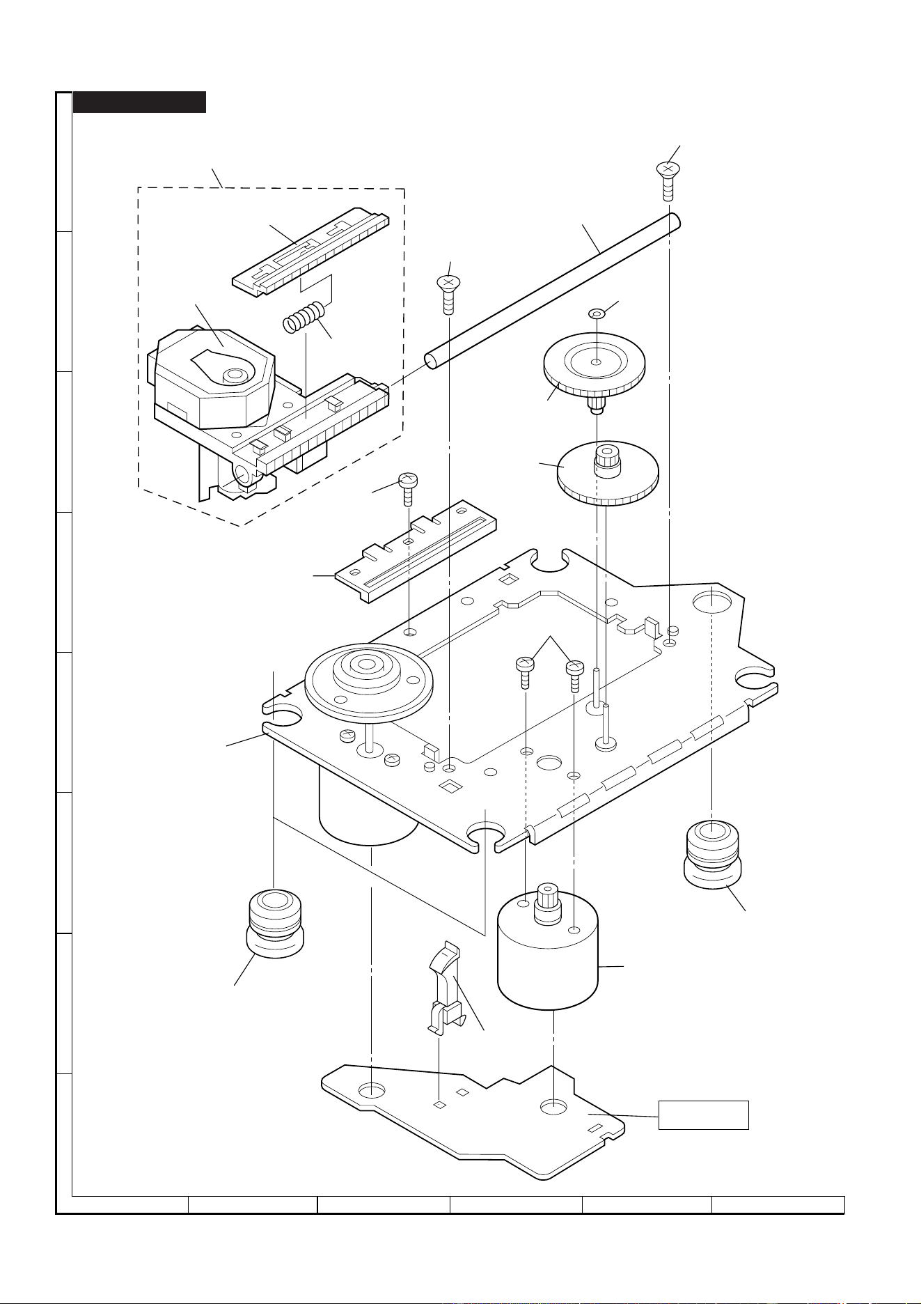
CD-E700H
A
B
C
D
E
F
G
H
1
23456
Figure 7 CD MECHANISM EXPLODED VIEW
– 7 –
306-1
701
304
701
302
301
702
303
M1
703x2
305x2
SW4
M2
305
PWB-D
306-2
306-3
306
704
CD-E700H
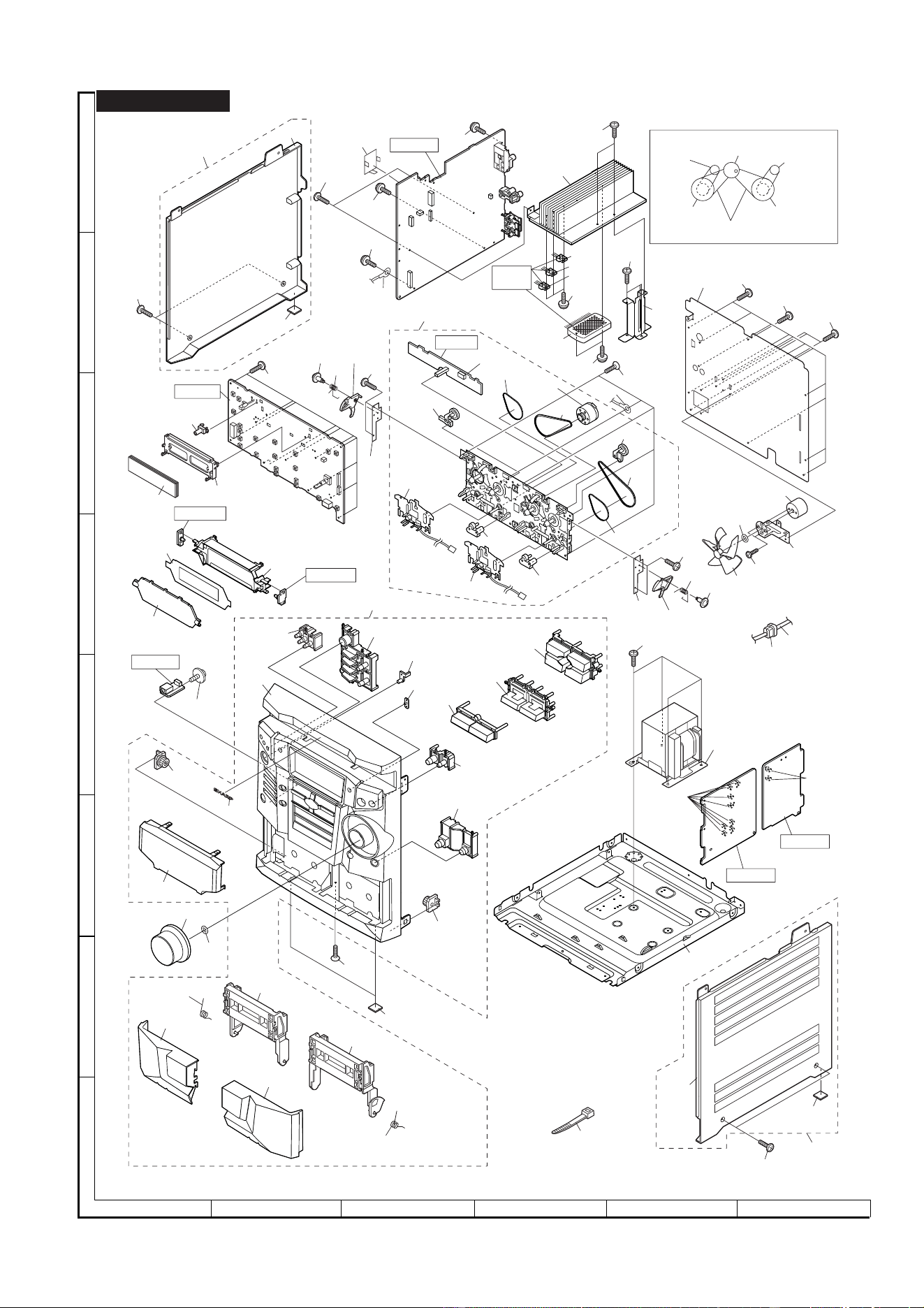
CD-E700H
A
B
C
D
E
F
G
H
1
23456
Figure 8 CABINET EXPLODED VIEW (1/2)
– 8 –
Note: Only the unit and consumable parts are supplied as parts supply for the Tape mechanism.
PWB-A4
PWB-A5
257
254
253
202
601x2
202-1
202-2
PWB-A1
246
244
252
604x2
611
260
611
601x2
614x3
616x2
615x3
IC851
IC901
IC852
IC853
611
Tape
Motor
MAIN BELT
FLYWHEEL
ASS'Y
TAPE1
FLYWHEEL
ASS'Y
TAPE2
FF/REW
ROLLER
ASS'Y
FF/REW
ROLLER
ASS'Y
BELT CONNECTION
601x11
614x3
601
207
M901
248
234
212
213
245
211
610x2
PWB-A2
219
220
FL701
617x10
PWB-A3
603
201
PT801
609x4
247x2
247x8
PWB-B2
PWB-B1
250
601x2
201-15
201-16
612
242x2
203
203-2
203-1
Silicon
Grease
201-7
201-19
201-17
201-14
201-11
201-10
201-9
201-8
201-6
201-3
201-5
201-4
201-2
255
201-1
201-13
201-12
201-17
248
201-18
618x5
246
208
208-9
208-11
208-6
208-6
208-5
208-4
208-7
208-3
208-8
208-2
208-10
208-1
605
230
606x2
227
209
PWB-F
606x2
210
228
231
605
CD-E700H
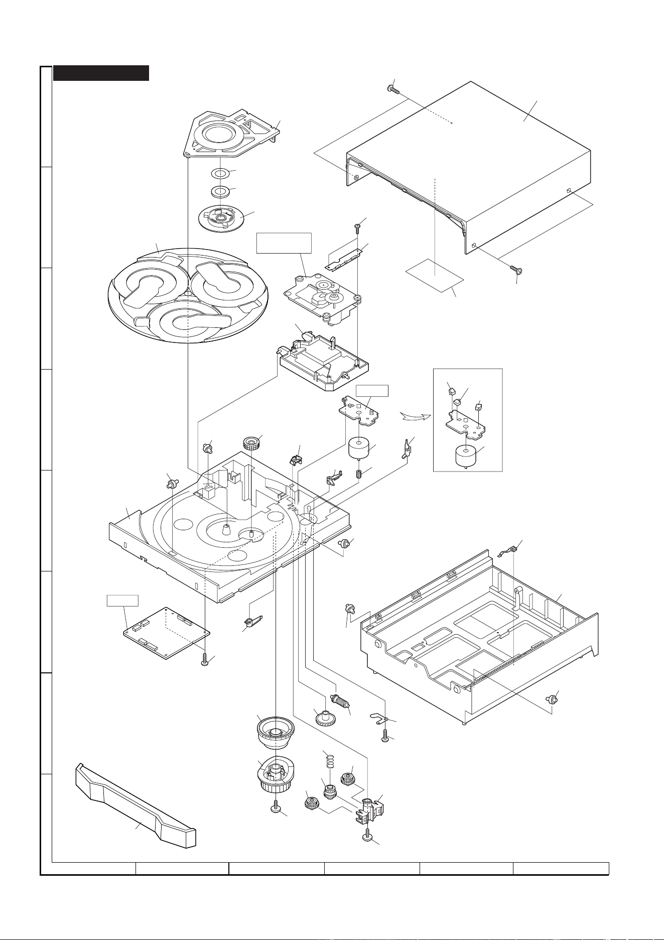
CD-E700H
A
B
C
D
E
F
G
H
1
23456
217
243
258
215
620x2
241
249
602x2
205
602x2
M3
SW3
M3
SW2
SW1
251
PWB-E
226
224
223
619x2
229
236
237
236
222
221
218
240
225
239
238
CD
MECHANISM
216
251
235
PWB-C
251
251
251
204
214
232
608
233
607
607
206
259
Figure 9 CABINET EXPLODED VIEW (2/2)
– 9 –
CD-E700H
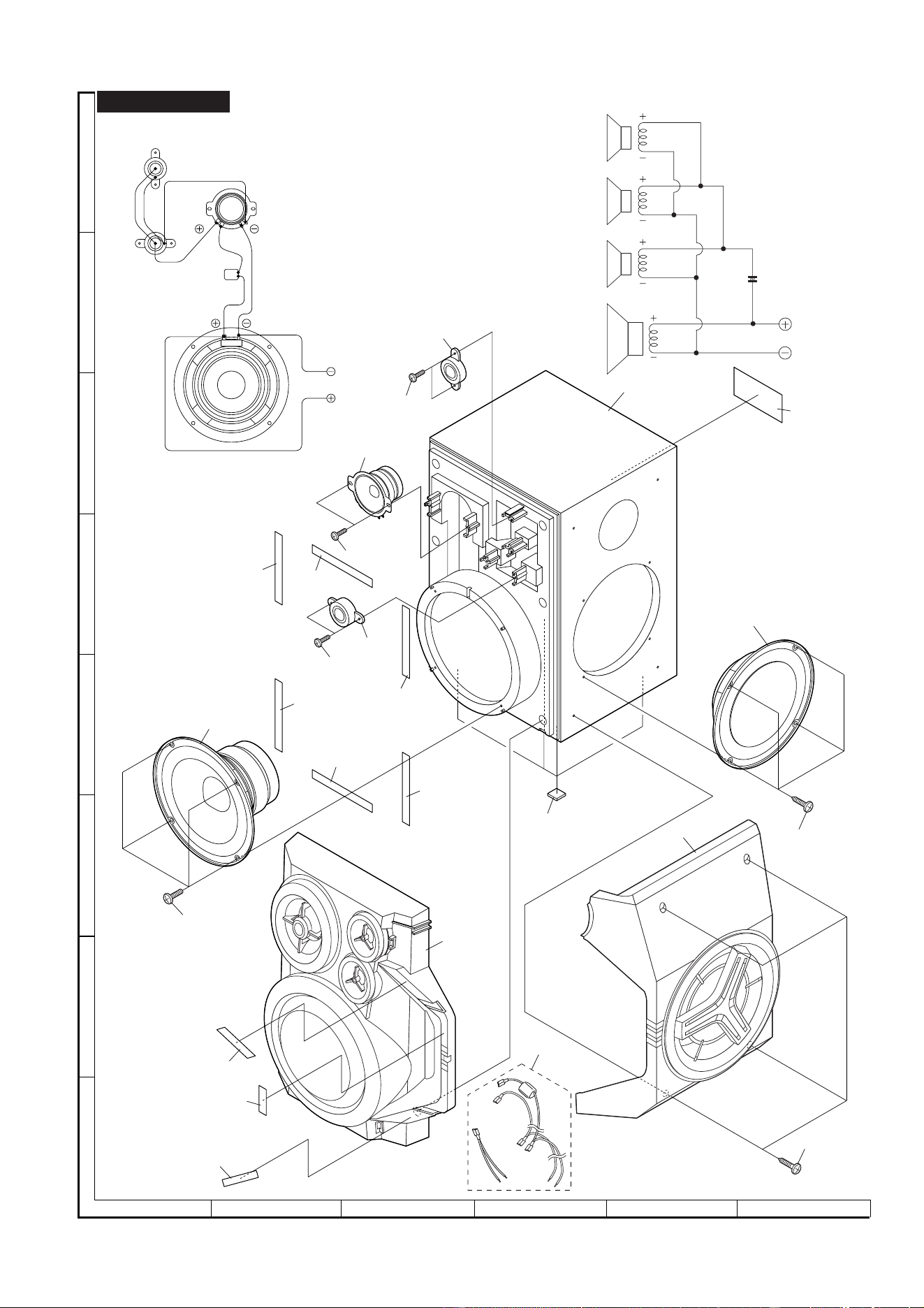
CD-E700H
A
B
C
D
E
F
G
H
1
23456
Figure 10 SPEAKER EXPLODED VIEW
– 10 –
SP1, 2
SP1, 2
SP3,4
SP5,6
SP7, 8
WOOFER
SP3, 4
TWEETER
BK
RD
BKRD
RD
SP7, 8
SUPER TWEETER
SP5, 6
SUPER TWEETER
SP3,
TWEETER
SP5,
SUPER TWEETER
SP7,
SUPER TWEETER
SP1,
WOOFER
RD
RD
BK
BK
100V (N.P.)
Electrolytic
C2
Capacitor
2.2µF,
C1,
100V (N.P.)
Electrolytic
C2
Capacitor
2.2µF,
C1,
4
6
8
2
901
909
904
912x4
908x4
906x2
906x2
906x2
903
907x4
905x4
911
910
902
913
913
913
910
910
910
910
910
CP-E700H

CD-E700H
COPYRIGHT 2003 BY SHARP CORPORATION
ALL RIGHTS RESERVED.
No part of this publication may be reproduced,
stored in a retrieval system, or transmitted in
any form or by any means, electronic, mechanical,
photocopying, recording, or otherwise, without
prior written permission of the publisher.
A0302-001DS•HA•M
SG
SHARP CORPORATION
AV Systems Group
Audio Systems Division
Higashihiroshima, Hiroshima 739-0192, Japan
Printed in Japan
©