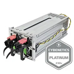

GM500-G
GEMINI SERIES
Endless power through redundancy
500+500W 24hour fully continuous power output
PS2 mini redundant power with 150mm(W) x 85mm(H) x 180mm(D)
80 PLUS Gold Certified
Active PFC (full range)
1+1 redundant configuration
Hot swappable design
Convenient pull-out handle bars
Industry-leading reliability
Support PMBus 1.2
The following manual and guides were carefully prepared by the SilverStone engineering team to
help you maximize the potential of your SilverStone product. Please keep this manual for future
reference when upgrading or performing maintenance on your system. A copy of this manual can also
be downloaded from our website at:
Installation and system optimization guide:
Specification
General
AC input specifications
DC output specification
Protection
Environmental requirements
Agency requirements
Redundant power supply function
PMBus
Reliability
Physical characteristics size
P.1
P.1
P.1
P.2
P.5
P.6
P.6
P.7
P.8
P.12
P.12

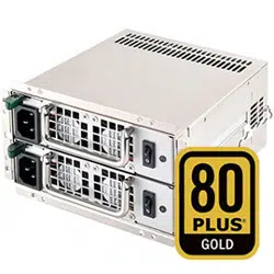
SPECIFICATION
SilverStone GEMINI
GM500-G
Mini Redundant Switching Power Supply
80 PLUS Gold
PMBus 1.2
500W+500W
01
This is the specification of Model GM500-G; it is intended to describe the functions and performance of the mini
redundant power supply. The GM500-G 500 watts mini redundant power supply is featured with Active PFC
(Power Factor Correction) capability and gold efficiency for 80+ and PMBus function meets IEC61000-3-2 and
equips full range Input features.
The power supply must meets inrush requirements of any rated AC voltage, during turn on at any phase of
voltage, during a single cycle AC dropout condition, during repetitive On/Off cycling of AC, and over the specified
temperature range. The peak inrush current shall be 30/60A @ 115/230 VAC (25℃) per module when cold start
and less than the rating of its critical components (including input fuse, bulk rectifiers, and surge limiting device).
The power supply must operate within all specified limits over the input voltage range in Table 1.Harmonics
distortion of up to 10% THD must not cause the power supply to go out of specified limits.
Base on the minimum voltage and power transfer, the max current calculation as below:
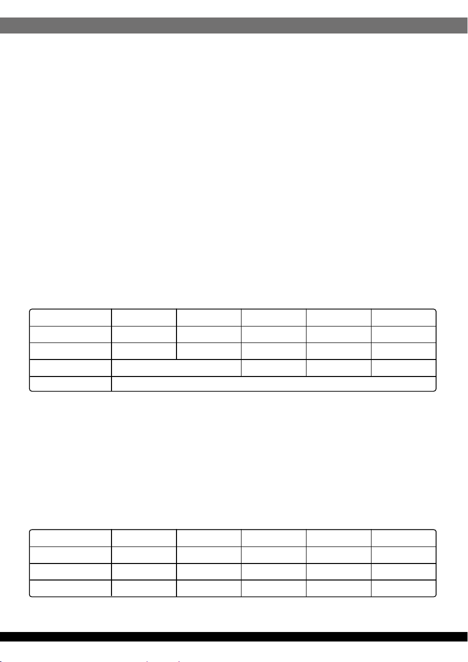
Table 1 – AC Input Voltage and Frequency
Max Current ≧ (Watt / Efficiency) / Minimum Voltage
2.2 AC inrush current
2.1 AC input voltage, frequency and current (Rating: 100V-240 VAC, 47-63Hz, 8-4A)
1. General
2. AC input specifications
Parameter
Voltage (115V)
Voltage (230V)
Frequency
Minimum
90 VAC
180 VAC
47 Hz
Normal
100-120 VAC
200-240 VAC
50 / 60 Hz
Maximum
132 VAC
264 VAC
63 Hz
Max. Current
8A
4A
N/A
02
2.3 Input power factor correction (Active PFC)
The power factor at 50% load shall be ≧ 0.9 at 230V input voltage.
2.4 Input current harmonics
When the power supply is operated in 90-264 VAC of Sec. 2.1, the input harmonic current drawn on the power
line shall not exceed the limits set by IEC61000-3-2 Class A and GB17625.1 standards. The power supply shall
incorporate universal power input with active power factor correction.
2.5 Dropout
An AC line dropout of 17mS or less shall not cause any tripping of control signals or protection circuits. If the
AC dropout lasts longer than 17mS, the power supply should recover and meet all turn on requirements. The
power supply shall meet the regulation requirement over all rated AC voltages, frequencies, and output loading
conditions. Any dropout of the AC line shall not cause damage to the power supply. An AC line dropout is
defined as a drop in AC line to 0 VAC at any phase of the AC line for any length of time.
3.1 Output current / loading
3.2 DC voltage regulation, ripple and noise
The following table defines power and current rating. The power supply shall meet both static and dynamic
voltage regulation requirements for minimum load condition.
The power supply output voltages must stay within the following voltage limits when operating at steady state
and dynamic loading conditions. All outputs are measured with reference to the return remote sense (Returns)
signal. The +5V, +3.3V, +12V, -12V and +5VSB outputs are measure at the power supply connectors references
to Returns. The +5V and +3.3V is measured at its remote sense signal (+5VS, +3.3VS) located at the signal
connector.
Table 2– Output Loads Range 1
Note 1: Maximum continuous total DC output power should not exceed 550W.
3. DC output specification
Output Voltage
Max. Load
Min. Load
Max. Combined
Total Output
+5V
25A
1A
170W
500W
+3.3V
25A
1A
+12V
41A
1A
-
-12V
0.8A
0A
-
+5VSB
3.5A
0.1A
17.5W
Table 3 – Regulation, ripple and noise
Output Voltage
Load Reg.
Line Reg.
Ripple & Noise
+5V
+/-5﹪
+/-1﹪
50mV
+3.3V
+/-5﹪
+/-1﹪
50mV
+12V
+/-5﹪
+/-1﹪
120mV
-12V
+/-5﹪
+/-1﹪
120mV
+5VSB
+/-5﹪
+/-1﹪
50mV
03
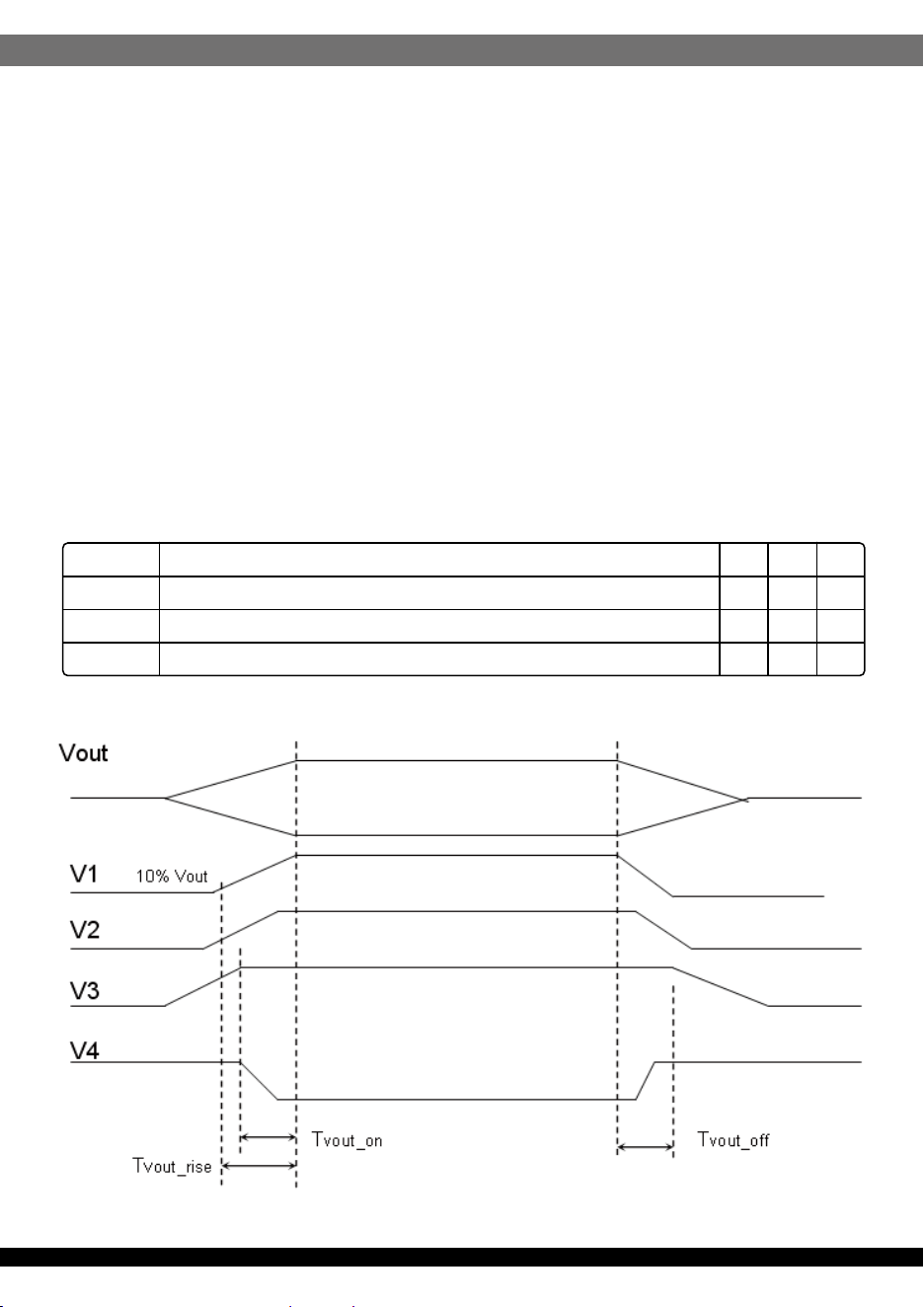
These are the timing requirements for the power assembly operation. The output voltages must rise from 10%
to within regulation limits (Tvout_rise) within 5 to 70mS. The +5V, +3.3V and +12V output voltages should start
to rise at about the same time. All outputs must rise monotonically. The +5V output must occur first than the
+3.3V output during any point of the voltage rise. The +5V output must never be greater than the +3.3V output
by more than 2.25V. Each output voltage shall reach regulation within 50 ms (Tvout_on) of each other during
turn on of the power supply. Each output voltage shall fall out of regulation within 400 mS (Tvout_off) of each
other during turn off. Figure 1 and figure 2 shows the turn on and turn off timing requirement. In Figure 2, the
timing is shown with both AC and PSON# controlling the on/off of the power supply.
Ripple and Noise shall be measured using the following methods:
a) Measurements made differentially to eliminate common-mode noise.
b) Ground lead length of oscilloscope probe shall be 0.25 inch.
c) Measurements made where the cable connectors attach to the load.
d) Outputs bypassed at the point of measurement with a parallel combination of 10uF tantalum capacitor in parallel
with a 0.1uF ceramic capacitors.
e) Oscilloscope bandwidth of 0 Hz to 20MHz.
f) Measurements measured at locations where remote sense wires are connected.
g) Regulation tolerance shall include temperature change, warm up drift and dynamic load.
3.3 Timing requirements
Table 4 – Output Voltage Timing
Item
Tvout_rise
Tvout_on
Tvout_off
Description
Output voltage rise time from each main output.(+5Vsb < 70mS)
All main output must be within regulation of each other within this time.
All main output must leave regulation within this time
MIN
5
N/A
N/A
MAX
70
50
400
Units
mS
mS
mS
Figure 1:Output Voltage Timing
04
3.4 Remote On/Off Control: PSON#
The PSON# signal is required to remotely turn on/off the power supply. PSON# is an active low signal that turns
on the +5V, +3.3V, +12V,-5V and –12V power rails. When this signal is not pulled low by the system, or left open,
the outputs (except the +5VSB and V bias) turn off. This signal is pulled to a standby voltage by a pull-up resistor
internal to the power supply.
Table 5 – Turn On/Off Timing
Item
Tsb_on-delay
Tac_on-delay
Tvout_holdup
Tpwok_holdup
Tpson_on_delay
Tpson_pwok
Tpwok_on
Tpwok_off
Tpwok_low
Tsb_vout
MIN
N/A
N/A
18
17
5
N/A
100
1
100
50
MAX
1500
2500
N/A
N/A
400
50
500
N/A
N/A
1000
Units
mS
mS
mS
mS
mS
mS
mS
mS
mS
mS
Description
Delay from AC being applied to +5VSB is being
within regulation.
Delay from AC being applied to all output voltages
being Within regulation.
All main output voltage stay within regulation after
loss of AC
Delay from loss of AC deassertion of PWOK.
Delay from PSON# active to output voltage within
regulation limits.
Delay from PSON# deactive to PWOK being
deasserted.
Delay from output voltage within regulation limits to
PWOK asserted at turn on.
Delay from PWOK deasserted to output voltages
(+5V, +3.3V, +12V) dropping out of regulation limits.
Duration of PWOK being in the deasserted state
during an off/on cycle using AC or the PSON# signal.
Delay from +5VSB being in regulation to O/Ps being
in regulation at AC turn on.
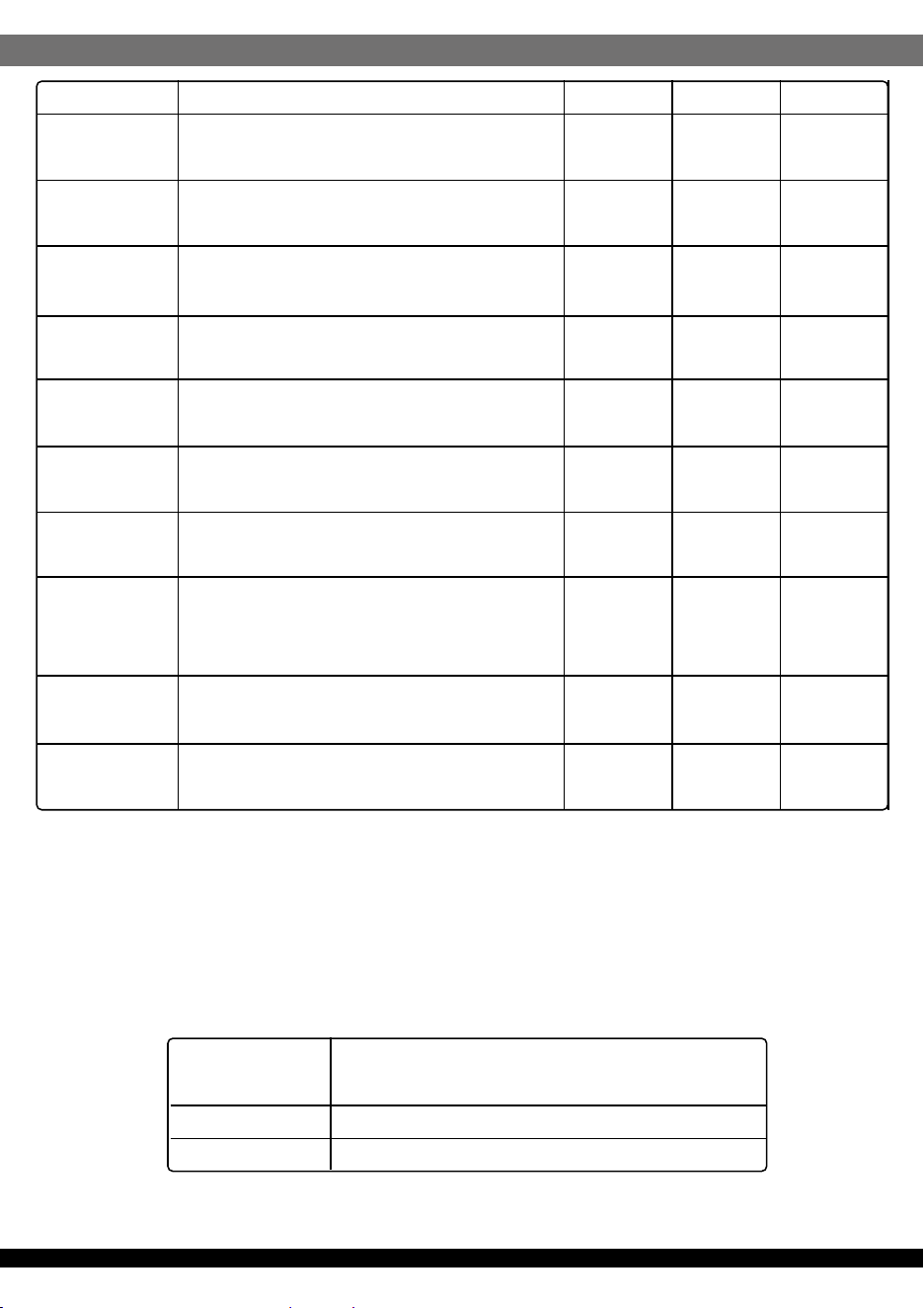
Table 6 – PWOK Signal Characteristic
Signal Type
PSON# = Low
PSON# = High
Accepts an open collector/drain input from the system.
Pull-up to VSB located in power supply.
Power ON
Power OFF
05
The efficiency should be measured module at 230 VAC and with external fan power source at specified loading.
3.5 Efficiency (80+ Gold)
The +5VSB output is always on (+5V Standby) when AC power is applied and power switch is turned on. The
+5VSB line is capable of delivering at a maximum of 3.5A for PC board circuit to operate.
3.6 +5VSB (Standby)
The OPP function shall work at 110%~160% of rating of output power, then all outputs shut down in a latch off
mode. The latch shall be cleared by toggling the PSON# signal or by cycling the AC power. The power supply
shall not be damaged from repeated power cycling in this condition. If only one module works inside the power
supply, the OPP is at 110%~160% of rating of power supply.
4.1 Over power protection
Each hot swap module has respective OVP circuit. Once any power supply module shut down in a latch off
mode while the output voltage exceeds the over voltage limit shown in Table 7, the other modules should
deliver the sufficient power to the device continually.
4.2 Over voltage protection
Input Voltage
230 VAC
20% Load
88%
50% Load
92%
100% Load
88%
Reference www.80plus.org all test conditions.
Voltage
+5V
+3.3V
+12V
5VSB
Minimum
+5.7V
+3.9V
+13.3V
+5.7V
Maximum
+6.5V
+4.5V
+14.5V
+6.5V
Shutdown Mode
Latch Off
Latch Off
Latch Off
Auto recovery
Table 7 –Over Voltage protection
Protection circuits inside the power supply shall cause only the power supply’s main outputs to shutdown. If the
power supply latches off due to a protection circuit tripping, either an AC cycle OFF for 15 sec or PSON #cycle
HIGH for 1 sec must be able to restart the power supply.
4. Protection
06
4.3 Over current protection
The power supply should contain the OCP function on each hot swap module. The power supply should be shut
down in a latch off mode while the respective output current exceeds the limit as shown in Table 8. When the latch
has been cleared by toggling the PSON# single or cycling the AC input power. The power supply module should
not be damaged in this condition.
4.4 Short circuit protection
5.1 Temperature
5.2 Humidity
6.1 Safety (Planning)
6.2 AC Input leakage current
The power supply shall shut down in a latch off mode when the output voltage is short circuit.
Input leakage current from line to ground will be less than 3.5mA rms. Measurement will be made at 240 VAC
and 60Hz.
Operating Temperature Range:
Non-Operating Temperature Range:
0°C ~ 40°C
-20°C ~ 70°C
Voltage
+5V
+3.3V
+12V
Minimum
110%
110%
110%
Maximum
160%
160%
160%
Shutdown Mode
Latch Off
Latch Off
Latch Off
Table 8 –Over Current protection
5. Environmental requirements
6. Agency requirements
Operating Humidity Range:
Non-Operating Humidity Range:
20% ~ 90%RH non-condensing
5% ~ 95%RH non-condensing
Product Safety:
UL60950-1/CSA 60950 (USA/Canada)
TÜV (CB) IEC60950 (report to include all country
national deviations)
EN60950-1(Europe)/IEC60950-1(International)
FCC(USA)
CE-low voltage directive 2006/95/EC(Europe)

07
The redundant power supply is N+1=N (500W+500W=500W) function power supply, each one module is
redundancy when any one module was failed. To be redundant each item must be in the hot swap power
supply module.
There is a single bi-color LED to indicate the power supply status. The Green LED turn ON to indicate that all
the power outputs are available. The Orange LED (Green+Red) turn ON to indicate that the power supply has
stand-by or failed shutdown due to over current, the Red LED turn ON to indicate the Fan of the power supply
has failed. The LED(s) shall be visible on the exterior face of the power supply. The LED location shall meet
ESD requirements. LED shall be securely mounted in such a way that incidental pressure on the LED shall not
cause displaced.
7.1 Redundancy
The redundant power supply modules shall be hot swappable. Hot swapping a power supply is the process of
inserting and extracting a power supply from an operating. During this process the output voltage shall remain
within the limits specified in Table 7 with the capacitive load specified Table 9. The Sub-system shall not exceed
the maximum inrush current as specified in section 2.2. The power supply can be hot swapped by the following
methods:
AC connects with each module. Up to two power supplies may be on a single AC power source. Extraction: The
AC power will be disconnected from the power supply first and then the power supply is extracted from the
sub-system. This could occur in standby mode or powered on mode. Insertion: The module is inserted into the
cage and then AC power will be connected to the power supply module.
For power modules with AC docking at the same time as DC. Extraction: The module is extracted from the cage
and both AC and DC disconnect at the same Time. This could occur in standby or power on mode. No damage
or arcing shall occur to the DC or AC contacts which could cause damage. Insertion: The AC and DC connect
at the same time as the module is inserted into the cage. No damage to the connector contacts shall occur. The
module may power on or come up into standby mode.
Many variations of the above are possible. Supplies need to be compatible with these different variations
depending upon the sub-system construction. In general, a failed (off by internal latch or external control) supply
may be removed, then replaced with a good power supply (must use the same model); however, hot swap needs
to work with operational as well as failed power supplies. The newly inserted power supply may get turned on
by inserting the supply into the system or by system management recognizing an inserted supply and explicitly
turning it on.
7.2 Hot swap requirements
7.3 LED Indicators
7. Redundant power supply function
08
8.2.1. Power supply management interface address
8.1 PMBus communication
The PMBus serial bus communication devices for I2C data in the power supply shall be compatible with both
SMBus 2.0 “high power” and I2C Vdd based power and drive. This bus shall operate at 3.3V but tolerant of 5V
signaling. The SMBus pull-ups are located on the motherboard and may be connected to 3.3V or 5V.
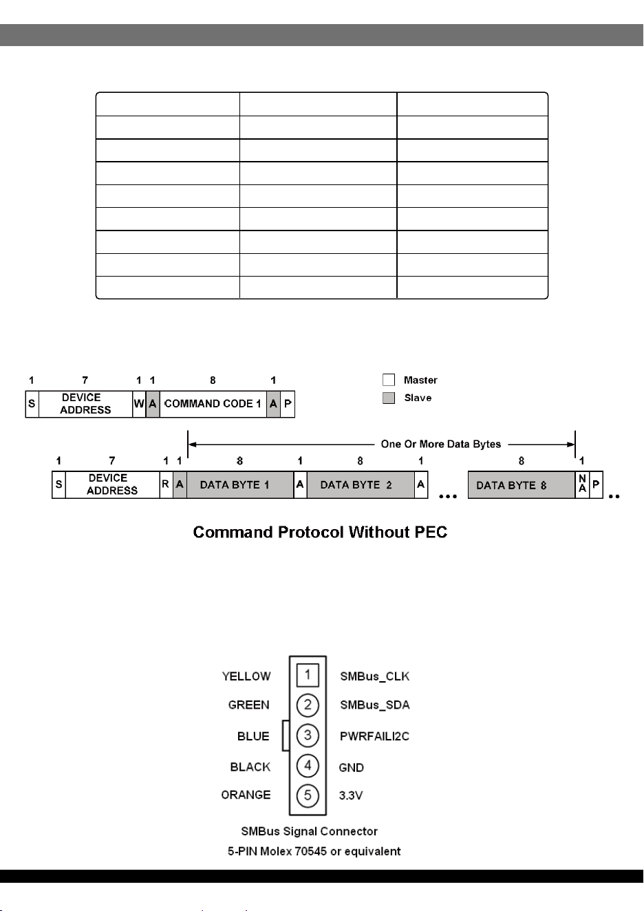
Two pins are allocated on the power supply. One pin is the serial clock (SMBus_SCL). The second pin is used
for serial data (SMBus_SDA). Both pins are bi-directional and are used to form a serial bus.
The device(s) in the power supply shall be located at an address(s) determined by addressing pins A0 and A1
on the power supply module. The circuits inside the power supply shall derive their power from the 5VSB bus.
Device(s) shall be powered from the system side of the 5VSB device. No pull-up resistors shall be on SCL or
SDA inside the power supply. There pull-up resistors should be located external to the power supply.
8.2 Power supply management interface
The device in the power supply shall derive its power off of the 5VSB output on the system side. It shall be
located at an address set by the A0 and A1 pins. Refer to the PMBus specification posted on the www.powerSIG.org
website for details on the power supply monitoring interface requirements. I2C is a SMBus interface used to
communicate power management information to the system.
Device address locations
PDB addressing A1/A0
Device Address
Housing
-
-
M1
1/1
B6h
M2
0/1
B2h
8. PMBus

09
8.2.2. PMBus command code summary
PMBus Revison1.2 specification shall be used for the communication with system.
Command code
19h
1Ah
88h
89h
8Bh
8Ch
8Dh
90h
91h
96h
97h
98h
99h
9Ah
9Bh
9Eh
A0h
A1h
A7h
B0h
D0h
D1h
D2h
D3h
D4h
D5h
Command Name
CAPABILITY
QUERY
READ_ACV_IN
READ_ACI_IN
READ_VOUT
READ_IOUT
READ_TEMPERATURE_1
READ_FAN1_SPEED
READ_ FAN2_SPEED
READ_POUT
READ_PIN
PMBus_REVISION
MFR_ID
MFR_MODEL
MFR_ REVISION
MFR_SERIAL
MFR_VIN_MIN
MFR_VIN_MAX
MFR_POUT_MAX
USER_DATA_00
Reserved
Reserved
Reserved
Reserved
READ_AC_PFC
READ_ AC_FREQUENC
SMBus Transaction Type
READ BYTE
READ BYTE
READ WORD
READ WORD
READ WORD
READ WORD
READ WORD
READ WORD
READ WORD
READ WORD
READ WORD
READ BYTE
R/W Block
R/W Block
R/W Block
R/W Block
READ WORD
READ WORD
READ WORD
READ BYTE
-
-
-
-
READ WORD
READ WORD
Number of Data Bytes
1
1
2
2
2
2
2
2
2
2
2
1
16
16
2
16
2
2
2
1
2
2
2
2
2
2
(Data Byte Type ASCII Code or HEX Code)

10
MFR-Manufacturer
Command code
19h
1Ah
88h
89h
8Bh
8Ch
8Dh
90h
91h
96h
97h
98h
99h
9Ah
9Bh
9Eh
A0h
A1h
A7h
B0h
D0h
D1h
D2h
D3h
D4h
D5h
Command Name
CAPABILITY
QUERY
READ_ACV_IN
READ_ACI_IN
READ_VOUT
READ_IOUT
READ_TEMPERATURE_1
READ_FAN_SPEED_1
READ_ FAN_SPEED_2
READ_POUT
READ_PIN
PMBus_REVISION
MFR_ID
MFR_MODEL
MFR_ REVISION
MFR_SERIAL_NO.
MFR_VIN_MIN
MFR_VIN_MAX
MFR_POUT_MAX
USER_DATA_00
Reserved
Reserved
Reserved
Reserved
READ_AC_PFC
READ_ AC_FREQUENC
Meaning
-
-
239.88 V
2.499 A
12.100 V
24.000 A
38.5 ℃
12400 rpm
Reserved
250.00 W
500.0 W
1
SilverStone
SST-GM500-G
A0
201312120001
100 VAC
240 VAC
500W
Status Byte
-
-
-
-
0.9999
60.0HZ
VALUE ( ASCII or HEX CODE )
00H
F8H
5DH,B4H
09H,C3H
2FH,44H
5DH,C0H
01H,81H
30H,70H
00H,00H
61H,A8H
17H,70H
01H
4BH,49H,4EH,54H,52H,4FH,4EH,20H,
20H,20H,20H,20H,20H,20H,20H,20H
4DH,56H,50H,2DH,36H, 30H,30H,56H,
50H,50H, 20H,20H,20H,20H
41H,30H
32H,30H,31H,33H,31H,32H,31H,32H,30H,
30H,30H,31H,20H,20H,20H,20H
00H,64H
00H,F0H
02H,58H
00H
-
-
-
-
27H,0FH
02H,58H
(Data Byte Type ASCII Code or HEX Code)
11
Command code= B0h Command Name (USER_DATA_00)
8.2.3. PMBus Command Protocol
8.2.4. PMBus signal connector
Bit Number
7
6
5
4
3
2
1
0
Status Bit Name
Reserved
Reserved
Reserved
Reserved
Reserved
Reserved
PS_ON_Status
AC_Status (Must have12V)
Meaning
Default=0
Default=0
Default=0
Default=0
Default=0
Default=0
PS_OFF =0,PS_ON =1
AC OK =0,AC Fail =1
PMBus command protocol for the two steps (Figure 8.2.3-1). The first step is master device sends Device Address
and Command Code1 to slave device. The Command Code 1 is set what kind data will receive on master device.
The second step is the master device will receive one or more DATA BYTE coming slave device.
Figure 8.2.3-1

12
9.1 Mean time between failures (MTBF)
TThe MTBF of the power supply shall be calculated utilizing the Part-Stress Analysis method of MIL-217F or Bell
core RPP. The calculated MTBF of the power supply shall be greater than 100,000 hours under the following
conditions:
Full rated load
120V AC input
Ground Benign
25°C
9. Reliability
10.1 Dimension: 150(W) x 85m(H) x 180(D)
10. Physical characteristics size

NO. G11223830