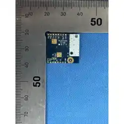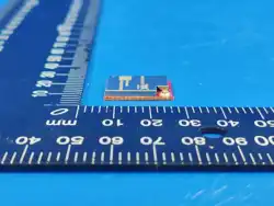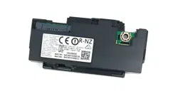
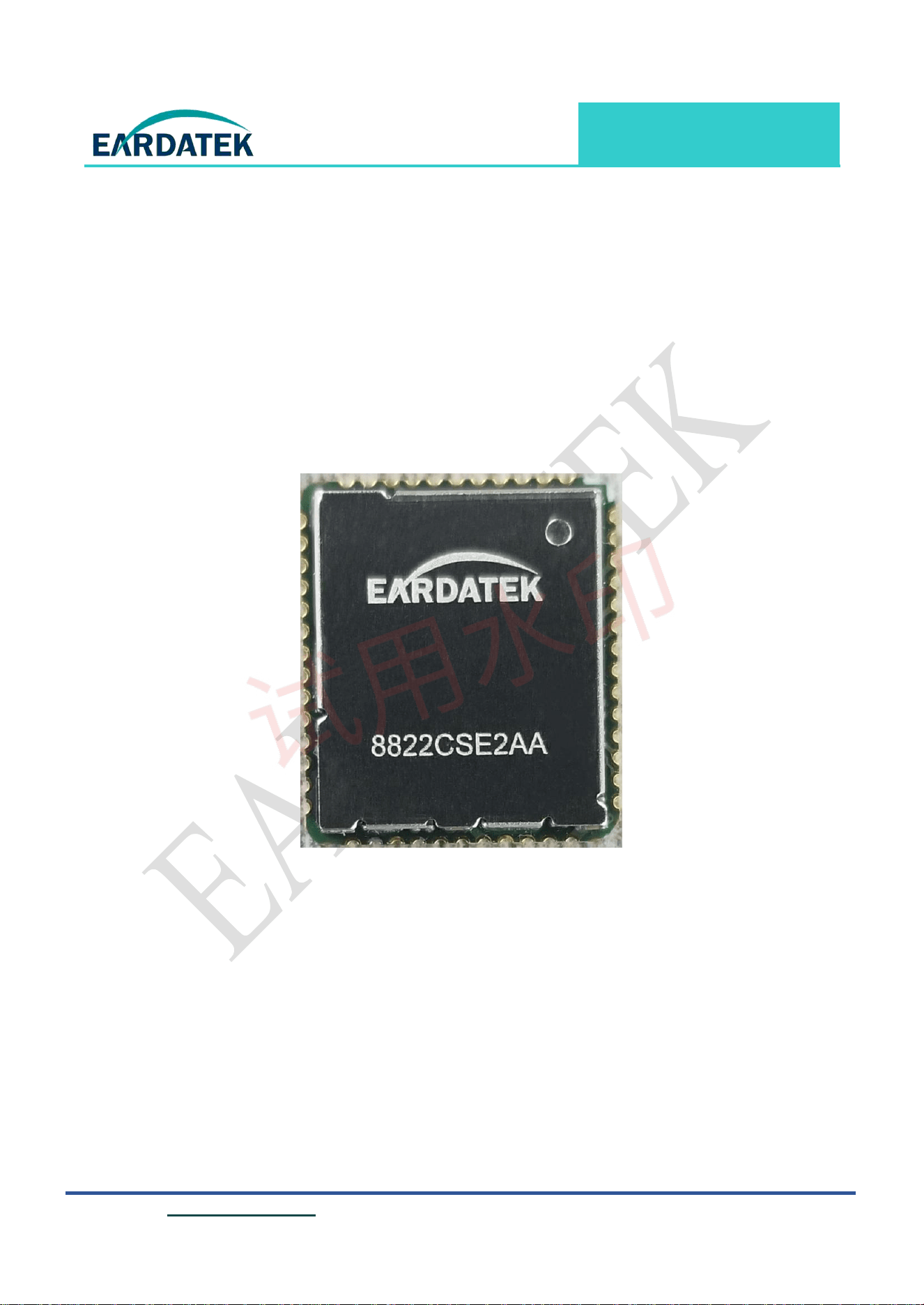
Module:EWN-8822CSE2AA
Contents
1 General Specifications ........................................................................................................... - 3 -
2 Features ................................................................................................................................... - 3 -
2.1 WLAN ........................................................................................................................................... - 3 -
2.2 Bluetooth ....................................................................................................................................... - 4 -
3 System Block Diagram........................................................................................................... - 4 -
4 PHY Specification .................................................................................................................. - 5 -
4.1 Wi-Fi Specification ....................................................................................................................... - 5 -
4.2 BT Specification ............................................................................................................................ - 7 -
5 Other Specifications ............................................................................................................... - 8 -
6 DC Characteristics ................................................................................................................. - 9 -
7 S11 Report ............................................................................................................................. - 10 -
8 Module configurations ......................................................................................................... - 12 -
9 Pin Definition ........................................................................................................................ - 13 -
10 Module Photos .................................................................................................................. - 16 -
11 Key material list ................................................................................................................ - 16 -
12 Package Information ........................................................................................................ - 17 -
13 Reference design ............................................................................................................... - 18 -
13.1 Power supply requirement ......................................................................................................... - 18 -
13.2 System power on sequence ......................................................................................................... - 20 -
13.3 SDIO Interface ............................................................................................................................ - 21 -
13.4 RF circuit ..................................................................................................................................... - 21 -
13.5 Application Circuit for SD_RESET and BT_DIS_N with Platform ...................................... - 24 -
13.6 Motherboard interference avoidance ....................................................................................... - 25 -
13.6.1 Interface interference ........................................................................................................................ - 25 -
13.6.2 The main chip interferes with DDR ................................................................................................. - 26 -
13.7 Recommended secondary reflux temperature curve .............................................................. - 27 -
14 Revision History ................................................................................................................ - 28 -
Module:EWN-8822CSE2AA
1 General Specifications
The module provides a complete solution for a high-performance integrated wireless and Bluetooth device. It
provides SDIO interface for Wi-Fi and HS-UART interface for Bluetooth. The module complies with IEEE
802.11 a/b/g/n/ac 2T2R MIMO standard, and Maximum PHY data rate up to 173.3 Mbps using 20 MHz band-
width ,400 Mbps using 40 MHz bandwidth, and 866.7 Mbps using 80 MHz bandwidth.
2 Features
2.1 WLAN
Supports 802.11ac 2x2, Wave-2 compliant with MU-MIMO
Completes 802.11n MIMO solution for 2.4GHz and 5GHz band
Maximum PHY data rate up to 173.3Mbps using 20MHz bandwidth, 400Mbps using 40 MHz band-
width, and 866.7Mbps using 80MHz bandwidth
Backward compatible with 802.11a/b/g devices while operating at 802.11n data rates
Backward compatible with 802.11a/n devices while operating at 802.11ac data rates
Complies with SDIO 1.1/2.0/3.0 for WLAN with clock rate up to 208MHz
support standard SDIO v3.0 (up to SDR104 mode at 208 MHz) host interfaces
complies with HS-UART with configurable baud rate for Bluetooth
IEEE 802.11a/b/g/n/ac compatible WLAN
IEEE 802.11e QoS Enhancement(WMM)
IEEE 802.11i (WPA, WPA2). Open, shared key and pair-wise key authentication
IEEE 802.11h DFS, TPC, Spectrum Measurement
IEEE 802.11k Radio Resource Measurement
WAPI (Wireless Authentication Privacy Infrastructure) certified
Channel management and co-existence
Wi-Fi Direct supports wireless peer to peer
CCA on secondary through RTS/CTS handshake
Supports TCP/UDP/IP checksum offload
Two Transmit and Two Receive paths
5MHz/10MHz/20MHz/40MHz/80MHz bandwidth transmission
Supports 2.4GHz and 5GHz band channels
Module:EWN-8822CSE2AA
Short Guard Interval(400ns)
Sounding packet
2.2 Bluetooth
Compatible with Bluetooth v2.1 and v3.0 Systems
Supports Bluetooth 4.1 features
Supports Bluetooth 4.2 LE Secure Connection by upper layer software upgrade
Support Bluetooth 5.0 and LE 5.0 system (BT5.2 Logo Compliant)
Supports all packet types in basic rate and enhanced data rate
Supports pico-nets in a scatter-net
Supports Secure Simple Pairing
Bluetooth 4.0 Dual Mode support: Simultaneous LE and BR/EDR
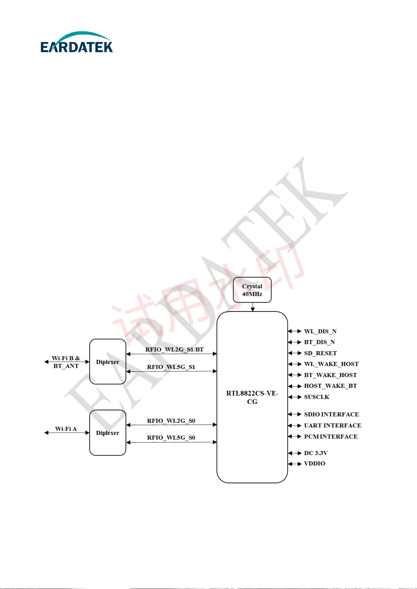
3 System Block Diagram
FIG 1 EWN-8822CSE2AA Block Diagram
Module:EWN-8822CSE2AA
Waiting for your suggestion at anytime. - 5 - E-mail:sales@eardatek.com
4 PHY Specification
4.1 Wi-Fi Specification
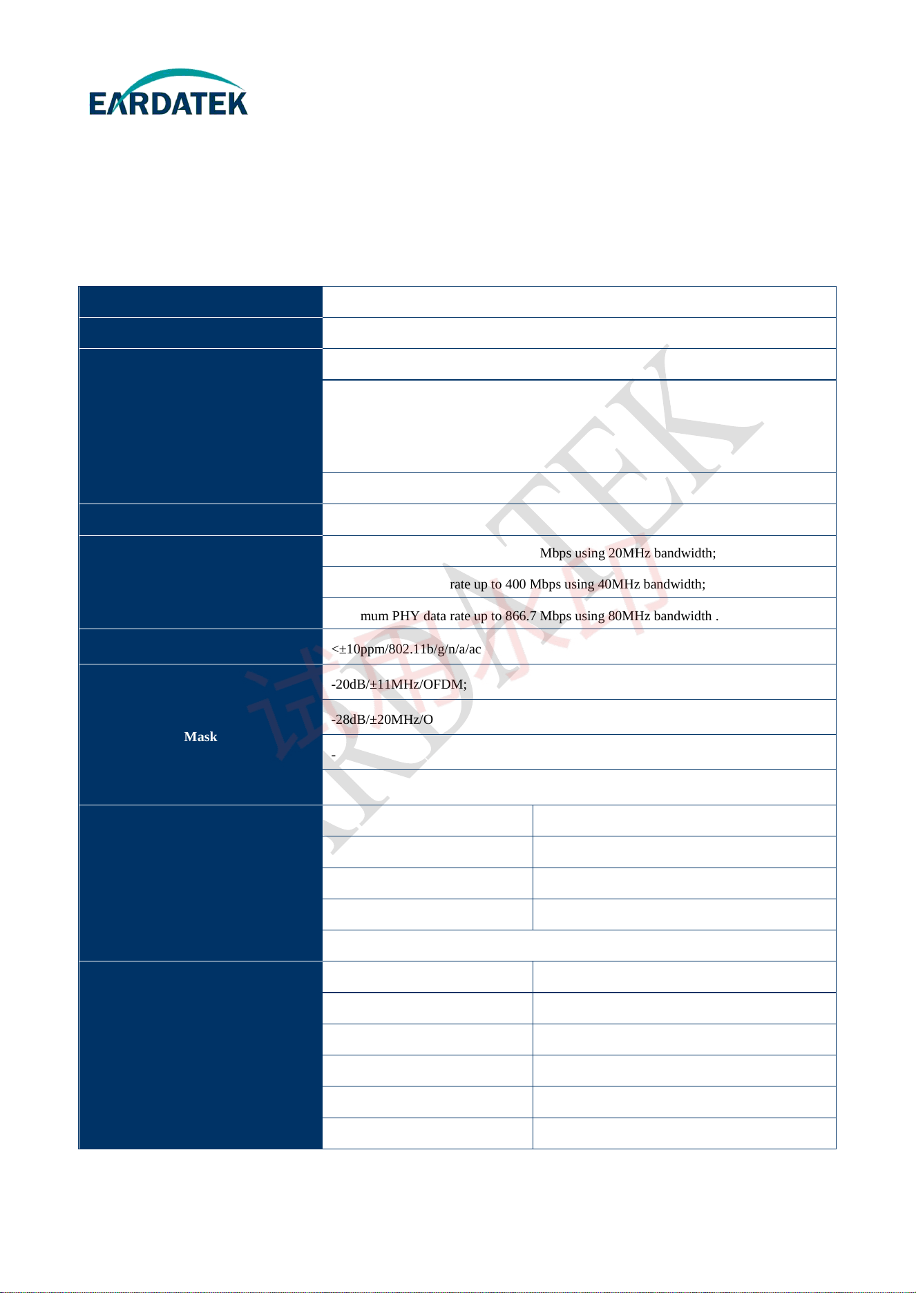
Table 1 EWN-8822CSE2AA Wi-Fi RF Parameters
Protocol IEEE 802.11b/g/n/a/ac
Interface SDIO 1.1 / 2.0 / 3.0
Frequency
2.4GHz band CH1~CH11/2400-2483.5MHz
5GHz Band CH36~CH48/5150-5250MHz
CH52~CH64/5250-5350MHz
CH100~CH144/5470-5725MHz
CH149~CH165/5725-5850MHz
2.4G&5G Band Refer to Channel Plan Domain Code
Bandwidth 20/40/80 MHz
PHY Rate
Maximum PHY data rate up to 173.3 Mbps using 20MHz bandwidth;
Maximum PHY data rate up to 400 Mbps using 40MHz bandwidth;
Maximum PHY data rate up to 866.7 Mbps using 80MHz bandwidth .
Frequency Error <±10ppm/802.11b/g/n/a/ac
Mask
-20dB/±11MHz/OFDM;
-28dB/±20MHz/OFDM;
-30dB/±11MHz/DSSS, CCK;
-50dB/±20MHz/DSSS, CCK.
2.4G
Transmit Power
802.11b (2.4G 11Mbps): 18 ±2dBm
802.11g (2.4G 54Mbps): 15 ±2dBm
802.11n (2.4G HT20 MCS7): 14 ±2dBm
802.11n (2.4G HT40 MCS7): 14 ±2dBm
Other TX power rate see the “power by rate”
2.4G
EVM
802.11b (2.4G 1Mbps): ≤-13dB
802.11b (2.4G 11Mbps): ≤-13dB
802.11g (2.4G 6Mbps): ≤-8dB
802.11g (2.4G 24Mbps): ≤-19dB
802.11g (2.4G 54Mbps): ≤-28dB
802.11n (2.4G HT20 MCS0): ≤-8dB
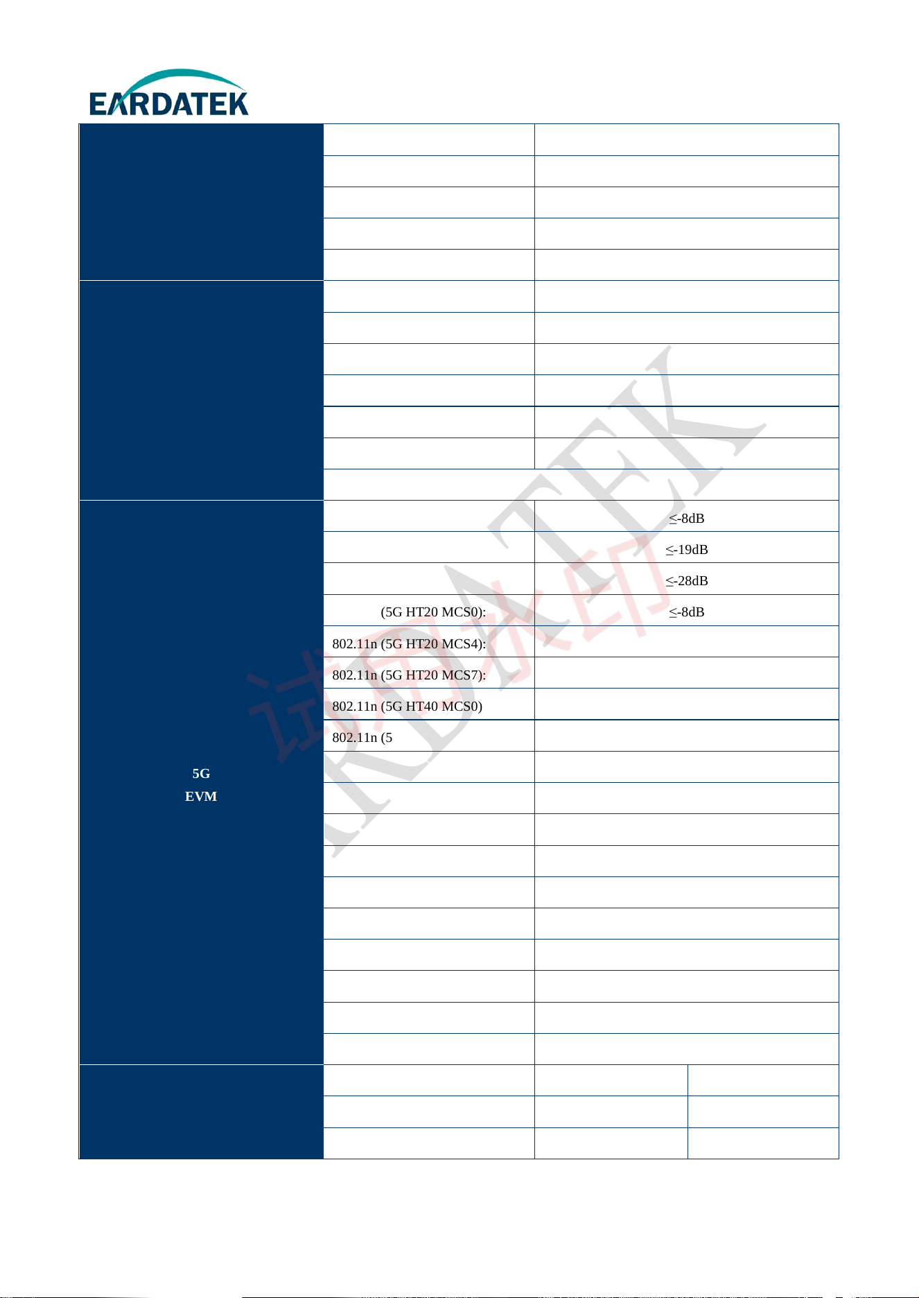
Module:EWN-8822CSE2AA
802.11n (2.4G HT20 MCS4): ≤-22dB
802.11n (2.4G HT20 MCS7): ≤-30dB
802.11n (2.4G HT40 MCS0): ≤-8dB
802.11n (2.4G HT40 MCS4): ≤-22dB
802.11n (2.4G HT40 MCS7): ≤-30dB
5G
Transmit Power
802.11a (5G 54Mbps): 15 ±2dBm
802.11n (5G HT20 MCS7): 14 ±2dBm
802.11n (5G HT40 MCS7): 14 ±2dBm
802.11ac (5G VHT20 MCS8): 13 ±2dBm
802.11ac (5G VHT40 MCS9): 12 ±2dBm
802.11ac (5G VHT80 MCS9): 12 ±2dBm
Other TX power rate see the “power by rate”
5G
EVM
802.11a (5G 6Mbps): ≤-8dB
802.11a (5G 24Mbps): ≤-19dB
802.11a (5G 54Mbps): ≤-28dB
802.11n (5G HT20 MCS0): ≤-8dB
802.11n (5G HT20 MCS4): ≤-22dB
802.11n (5G HT20 MCS7): ≤-30dB
802.11n (5G HT40 MCS0): ≤-8dB
802.11n (5G HT40 MCS4): ≤-22dB
802.11n (5G HT40 MCS7): ≤-30dB
802.11ac (5G VHT20 MCS0): ≤-8dB
802.11ac (5G VHT20 MCS5): ≤-25dB
802.11ac (5G VHT20 MCS8): ≤-33dB
802.11ac (5G VHT40 MCS0): ≤-8dB
802.11ac (5G VHT40 MCS5): ≤-25dB
802.11ac (5G VHT40 MCS9): ≤-35dB
802.11ac (5G VHT80 MCS0): ≤-8dB
802.11ac (5G VHT80 MCS5): ≤-25dB
802.11ac (5G VHT80 MCS9): ≤-35dB
2.4G
Receive Sensitivity
@ PER<10%
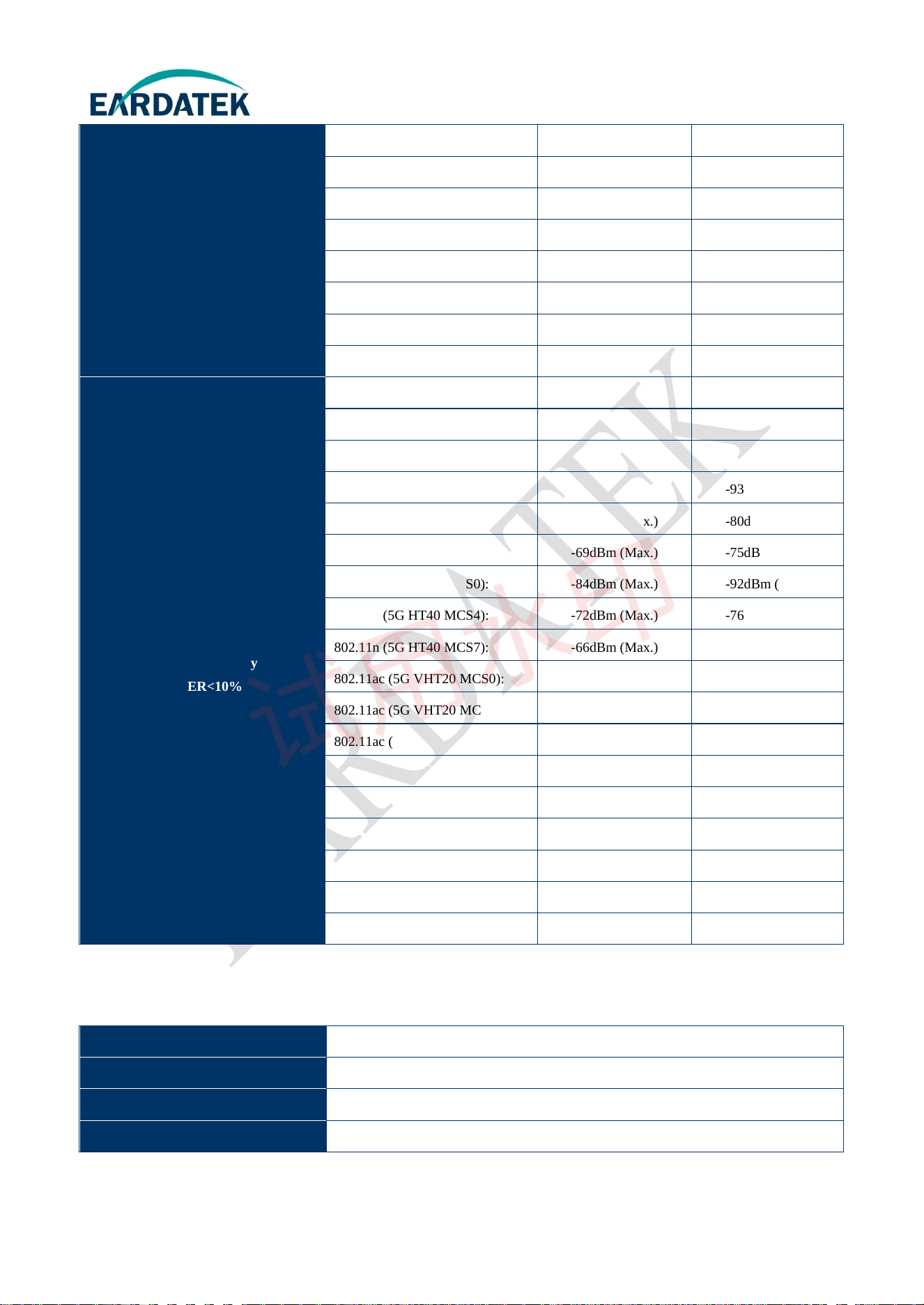
802.11b (2.4G 1Mbps): -91dBm (Max.) -97dBm (Typ.)
802.11b (2.4G 11Mbps): -85dBm (Max.) -91dBm (Typ.)
802.11g (2.4G 6Mbps): -87dBm (Max.) -96dBm (Typ.)
Module:EWN-8822CSE2AA
802.11g (2.4G 24Mbps): -79dBm (Max.) -83dBm (Typ.)
802.11g (2.4G 54Mbps): -70dBm (Max.) -77dBm (Typ.)
802.11n (2.4G HT20 MCS0): -87dBm (Max.) -95dBm (Typ.)
802.11n (2.4G HT20 MCS4): -75dBm (Max.) -80dBm (Typ.)
802.11n (2.4G HT20 MCS7): -69dBm (Max.) -75dBm (Typ.)
802.11n (2.4G HT40 MCS0): -84dBm (Max.) -92dBm (Typ.)
802.11n (2.4G HT40 MCS4): -72dBm (Max.) -76dBm (Typ.)
802.11n (2.4G HT40 MCS7): -66dBm (Max.) -73dBm (Typ.)
5G
Receive Sensitivity
@ PER<10%
802.11a (5G 6Mbps): -87dBm (Max.) -94dBm (Typ.)
802.11a (5G 24Mbps): -79dBm (Max.) -88dBm (Typ.)
802.11a (5G 54Mbps): -70dBm (Max.) -76dBm (Typ.)
802.11n (5G HT20 MCS0): -87dBm (Max.) -93dBm (Typ.)
802.11n (5G HT20 MCS4): -75dBm (Max.) -80dBm (Typ.)
802.11n (5G HT20 MCS7): -69dBm (Max.) -75dBm (Typ.)
802.11n (5G HT40 MCS0): -84dBm (Max.) -92dBm (Typ.)
802.11n (5G HT40 MCS4): -72dBm (Max.) -76dBm (Typ.)
802.11n (5G HT40 MCS7): -66dBm (Max.) -71dBm (Typ.)
802.11ac (5G VHT20 MCS0): -87dBm (Max.) -94dBm (Typ.)
802.11ac (5G VHT20 MCS5): -71dBm (Max.) -76dBm (Typ.)
802.11ac (5G VHT20 MCS8): -64dBm (Max.) -72dBm (Typ.)
802.11ac (5G VHT40 MCS0): -84dBm (Max.) -91dBm (Typ.)
802.11ac (5G VHT40 MCS5): -68dBm (Max.) -72dBm (Typ.)
802.11ac (5G VHT40 MCS9): -59dBm (Max.) -68dBm (Typ.)
802.11ac (5G VHT80 MCS0): -81dBm (Max.) -87dBm (Typ.)
802.11ac (5G VHT80 MCS5): -65dBm (Max.) -70dBm (Typ.)
802.11ac (5G VHT80 MCS9): -56dBm (Max.) -61dBm (Typ.)
4.2 BT Specification
Table 2 EWN-8822CSE2AA Bluetooth RF Parameters
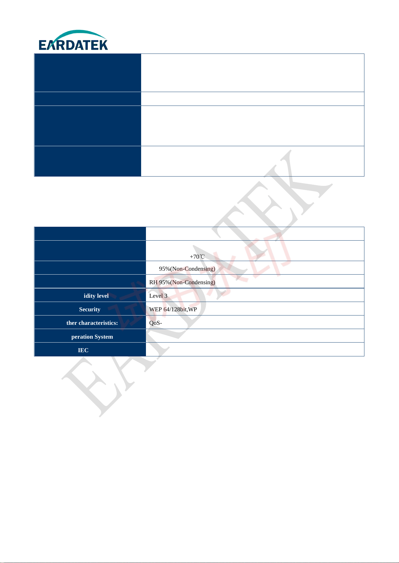
Protocol BTv2.1+EDR/BTv3.0/BT v4.2/BT v5.0
Interface UART
Frequency 2400 MHz ~ 2483.5 MHz (79 channels)
Modulation GFSK, π/4-DQPSK, 8-DPSK
Module:EWN-8822CSE2AA
PHY Rate
1Mbps for Basic Rate;
2、3 Mbps for Enhanced Data Rate;
1、2 Mbps for BLE
Transmit Power 6dBm, typical
Receive Sensitivity
<-89dBm @ BER=0.1% for GFSK (1Mbps);
<-90dBm @ BER=0.01% for π/4-DQPSK (2Mbps);
<-83dBm @ BER=0.01% for 8-DPSK (3Mbps);
<-90dBm @ PER=30.8% for BLE
Maximum Input level
GFSK(1Mbps): -20dBm;
π/4-DQPSK (2Mbps): -20dBm;
8-DPSK(3Mbps): -20dBm.
5 Other Specifications
Table 3 Other Specifications
Operating Temperature 0℃~+70℃
Storage Temperature
Module: -20℃~+125℃
Package: -20℃~+70℃
Operating Humidity RH 95%(Non-Condensing)
Storage Humidity RH 95%(Non-Condensing)
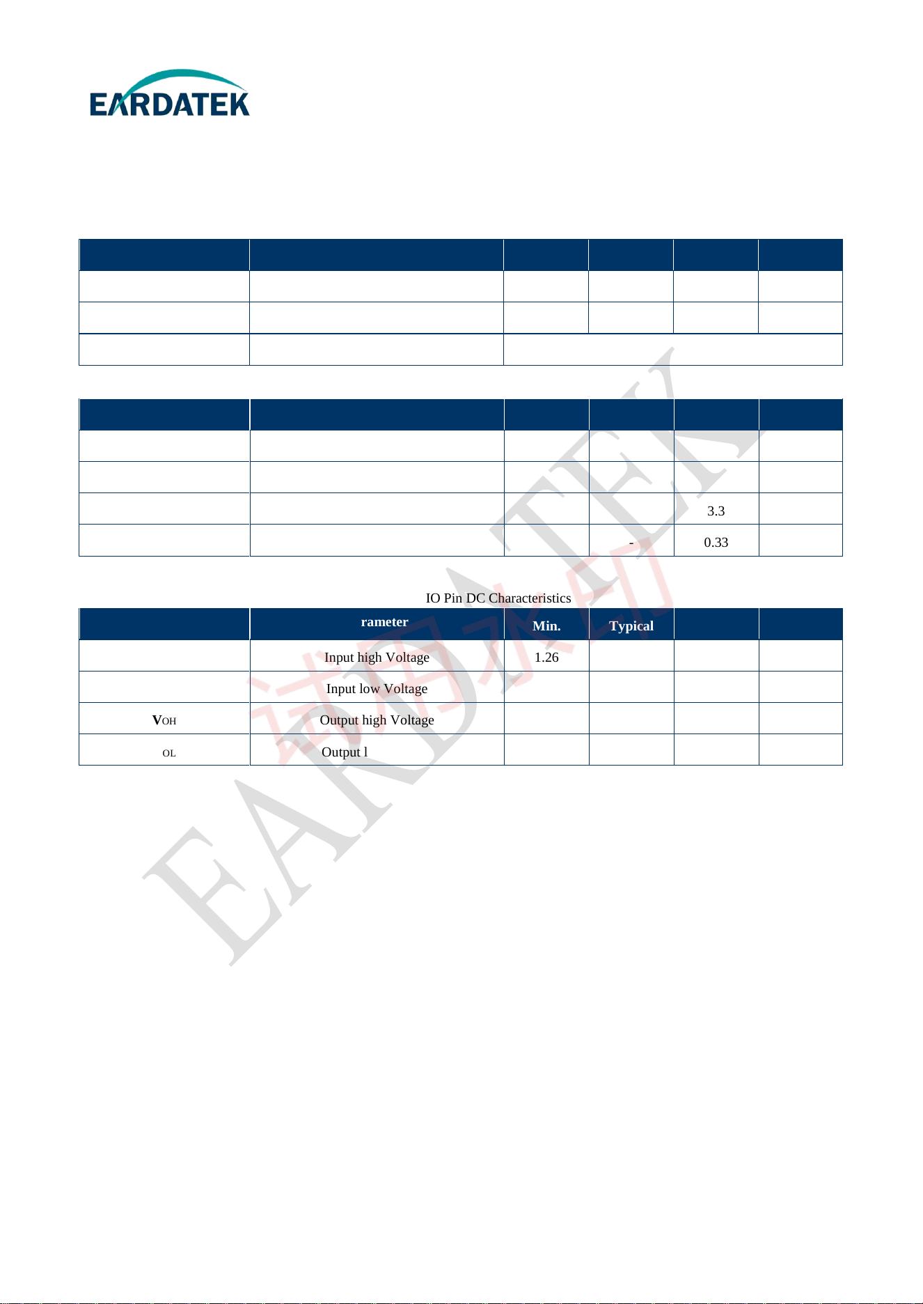
Humidity level Level 3
Security WEP 64/128bit,WPA,WPA2,TKIP,AES,WAPI
Other characteristics: QoS-WMM, WMM-PS
Operation System Windows XP/Win7/Linux/Android
ESD(IEC61000-4-2) ±1kV(Contact) @ RF Port
Module:EWN-8822CSE2AA
6 DC Characteristics
Table 4 Power Supply Characteristics
Symbol
Parameter
Min. Typical Max. Unit
VDD_3.3V 3.3V Supply Voltage 3.0 3.3 3.6 V
IDD_3.3V 3.3V Rating Current - - 1.5 A
VDDIO SDIO I/O Voltage Depend on the SDIO protocol (1.8V or 3.3V)
Table 5 3.3V IO Pin DC Characteristics
Symbol
Parameter
Min. Typical Max. Unit
VIH Input high Voltage 2.0 3.3 3.6 V
VIL Input low Voltage - 0 0.9 V
VOH Output high Voltage 2.97 - 3.3 V
VOL Output low Voltage 0 - 0.33 V
Table 6 1.8V IO Pin DC Characteristics
Symbol
Parameter
Min. Typical Max. Unit
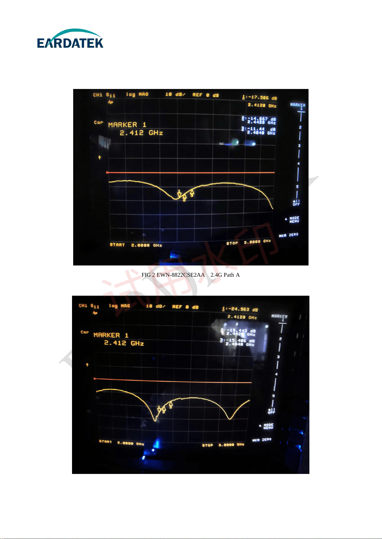
VIH Input high Voltage 1.26 1.8 3.6 V
VIL Input low Voltage - 0 0.8 V
VOH Output high Voltage 1.62 - 1.8 V
VOL Output low Voltage 0 - 0.18 V
Module:EWN-8822CSE2AA
Waiting for your suggestion at anytime. - 10 - E-mail:sales@eardatek.com
7 S11 Report
FIG 2 EWN-8822CSE2AA 2.4G Path A
FIG 3 EWN-8822CSE2AA 2.4G Path B
Module:EWN-8822CSE2AA
Waiting for your suggestion at anytime. - 11 - E-mail:sales@eardatek.com
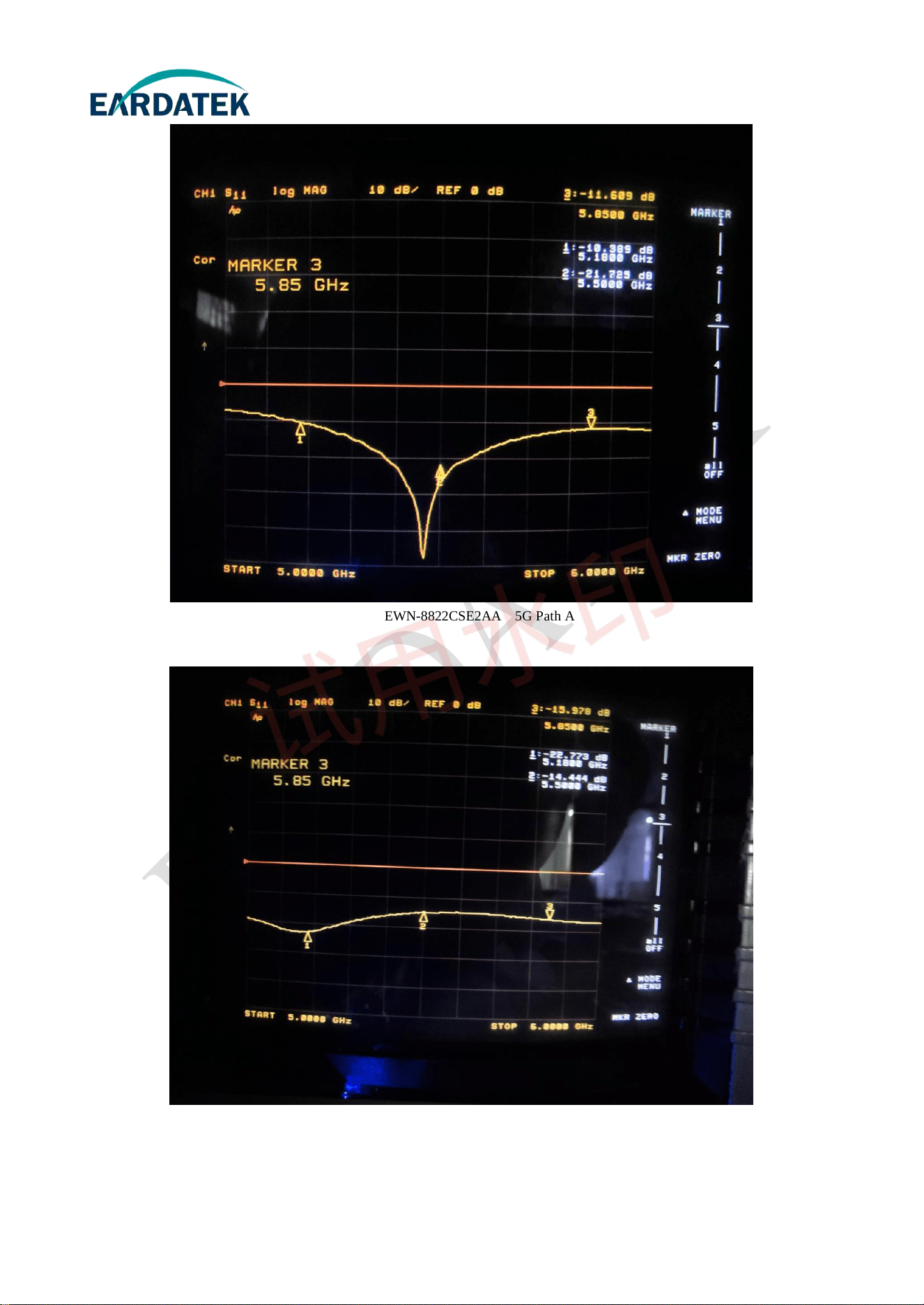
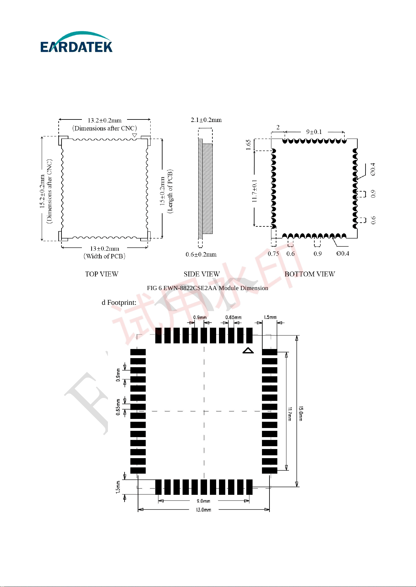
FIG 4 EWN-8822CSE2AA 5G Path A
FIG 5 EWN-8822CSE2AA 5G Path B
Module:EWN-8822CSE2AA
Waiting for your suggestion at anytime. - 12 - E-mail:sales@eardatek.com
8 Module configurations
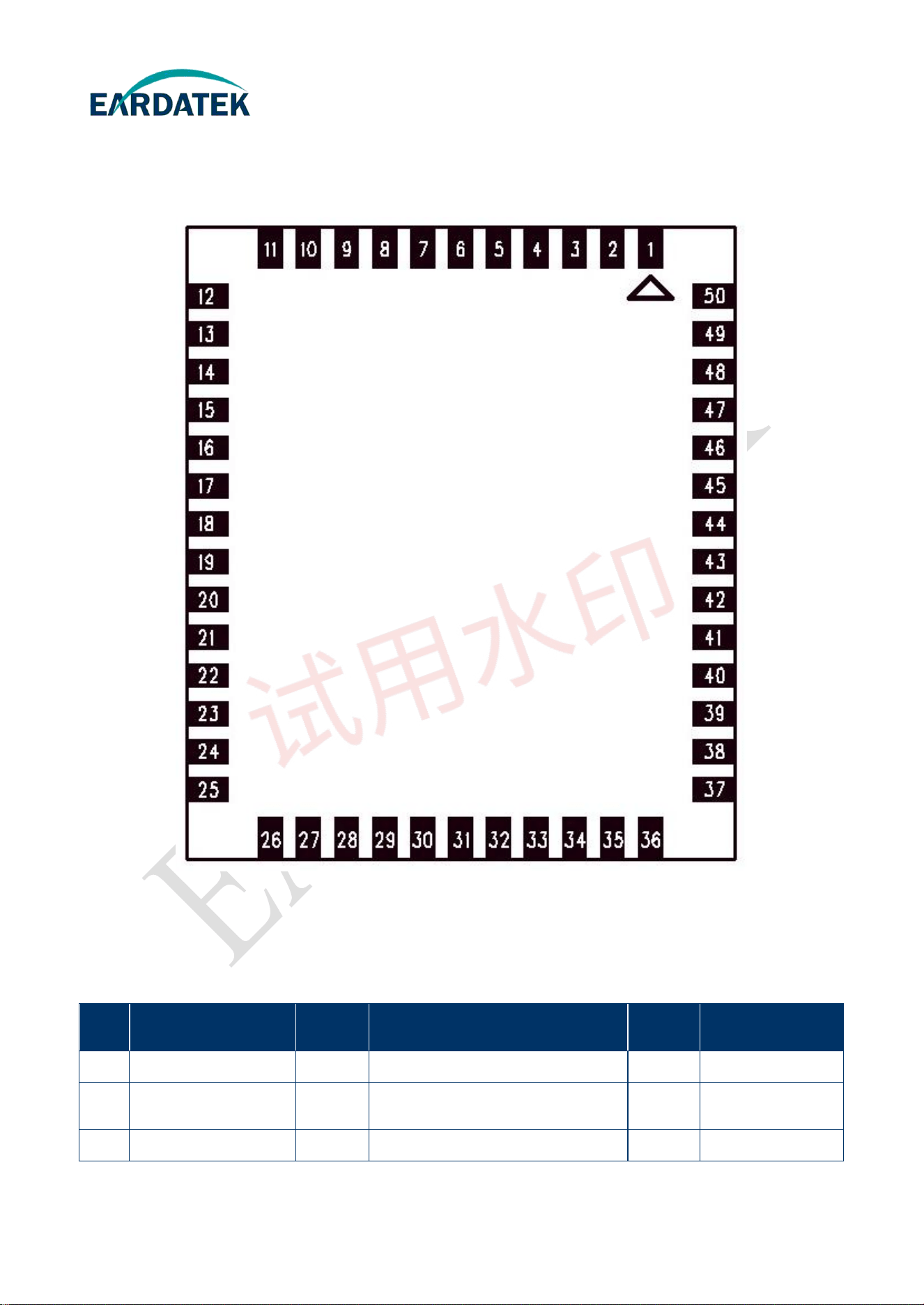
Module Dimension (L*W*T): 15.2±0.2mm*13.2±0.2mm*2.1±0.2mm。
FIG 6 EWN-8822CSE2AA Module Dimension
Recommended Footprint:
FIG 7 EWN-8822CSE2AA Recommended Footprint
Module:EWN-8822CSE2AA
Waiting for your suggestion at anytime. - 13 - E-mail:sales@eardatek.com
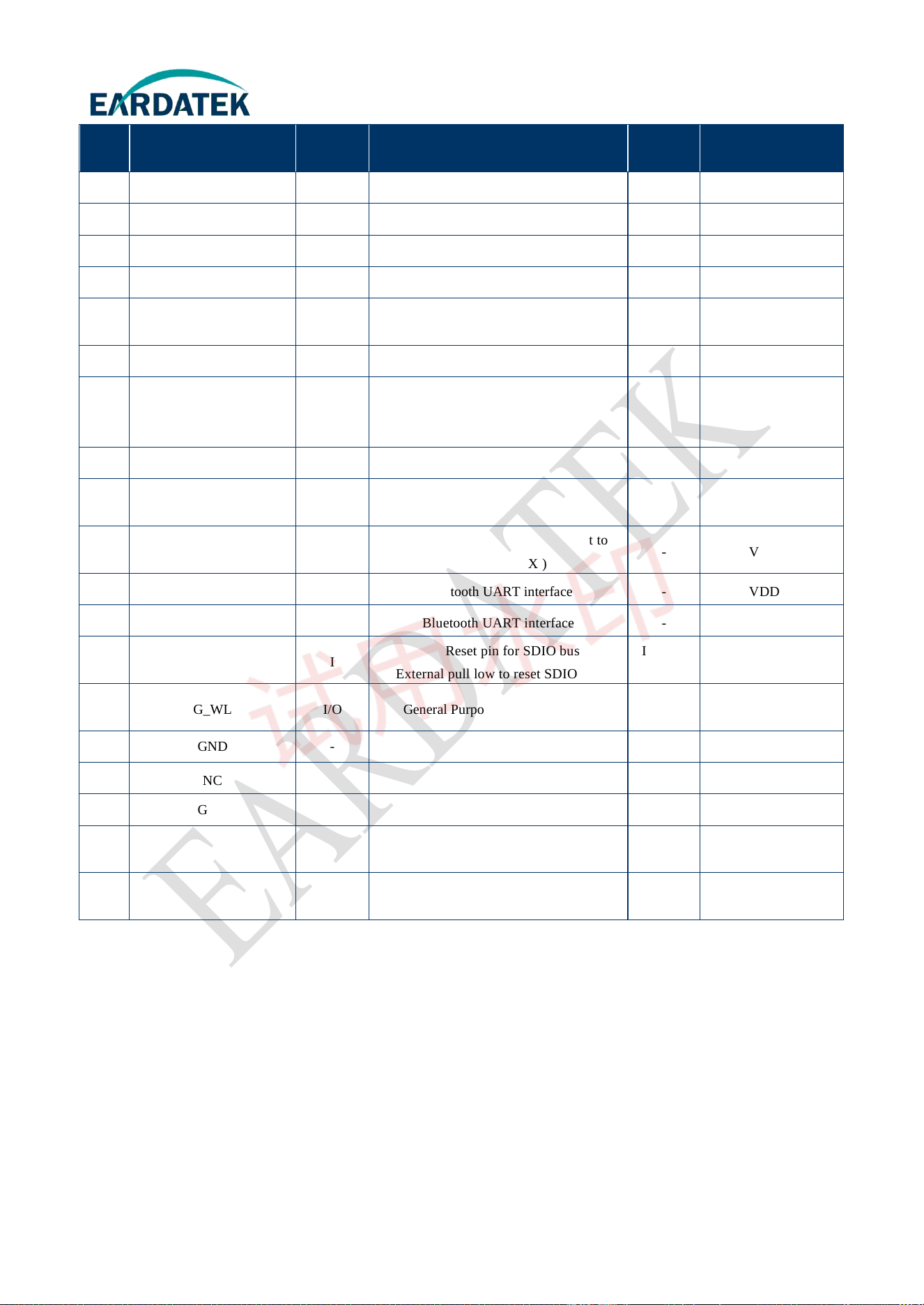
9 Pin Definition
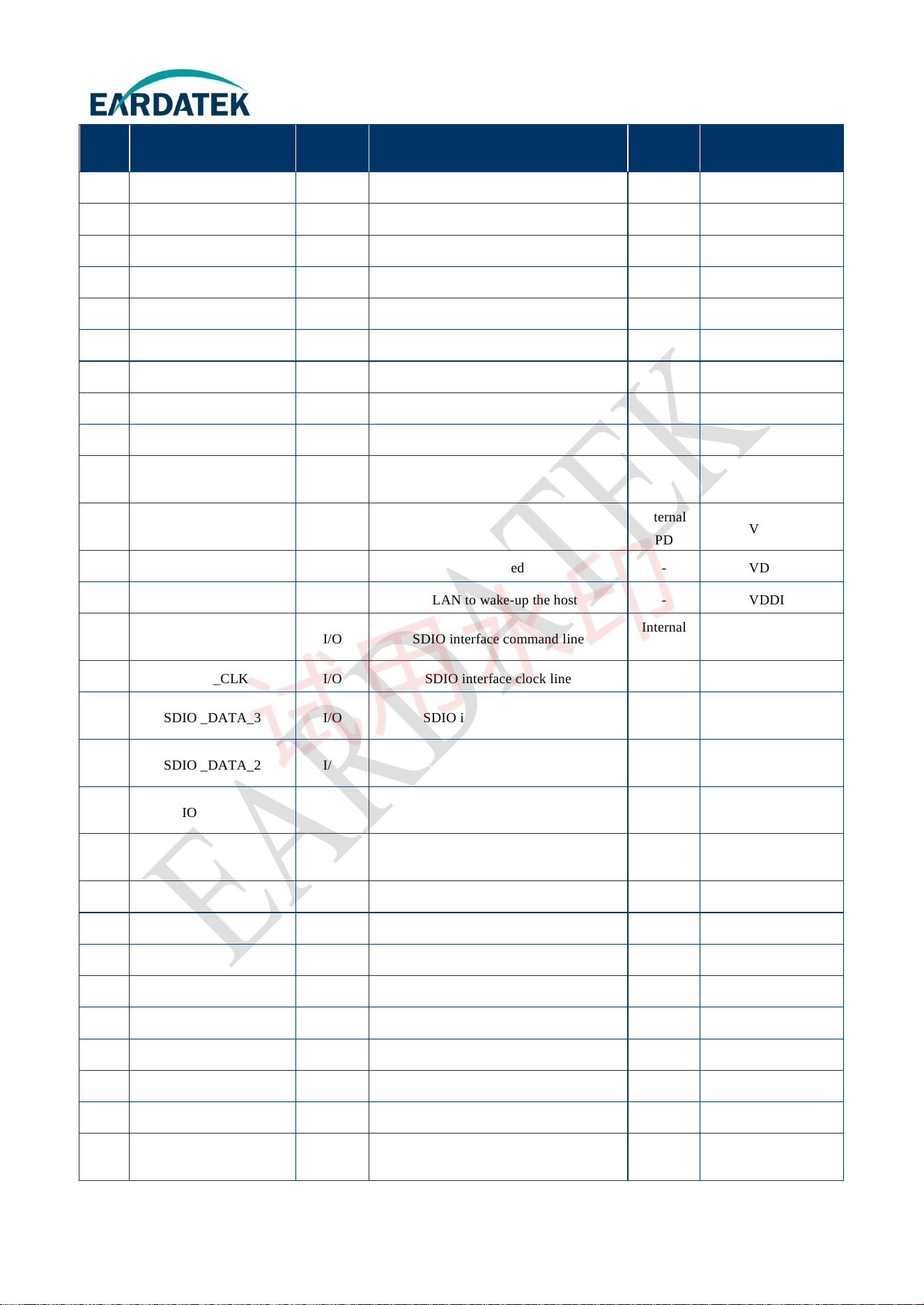
FIG 8 TOP VIEW
See Table 7 for the module hardware pin definition.
Table 7 EWN-8822CSE2AA Pin Description
Pin Definition Type Description
Default
Pull
Power level
1 GND - Ground - -
2 Wi-Fi B & BT_ANT I/O
Wi-Fi Path B ANT I/O port and Bluetooth
ANT I/O port
- -
3 GND - Ground - -
Module:EWN-8822CSE2AA
Waiting for your suggestion at anytime. - 14 - E-mail:sales@eardatek.com
Pin Definition Type Description
Default
Pull
Power level
4 GND - Ground - -
5 GND - Ground - -
6 GND - Ground - -
7 GND - Ground - -
8 GND - Ground - -
9
Wi-Fi A
I/O Wi-Fi Path A ANT I/O port - -
10 GND - Ground - -
11 GND - Ground - -
12
NC
- No connect - -
13 GPIO6 I/O General Purpose Input/Output Pin
Internal
PD
VDDIO
14 G_BT I/O General Purpose Input/Output Pin
Internal
PD
VDDIO
15 WL_DIS_N I Reserved - VDDIO
16 WL_WAKE_HOST O WLAN to wake-up the host - VDDIO
17 SDIO _CMD I/O SDIO interface command line
Internal
PU
VDDIO
18 SDIO _CLK I/O SDIO interface clock line - VDDIO
19 SDIO _DATA_3 I/O SDIO interface data line 3
Internal
PU
VDDIO
20 SDIO _DATA_2 I/O SDIO interface data line 2
Internal
PU
VDDIO
21 SDIO _DATA_0 I/O SDIO interface data line 0
Internal
PU
VDDIO
22 SDIO _DATA_1 I/O SDIO interface data line 1
Internal
PU
VDDIO
23 GND - Ground - -
24 WL_WAKE_HOST O WLAN to wake-up the host - VDDIO
25 GPIO7 I/O General Purpose Input/Output Pin - VDDIO
26 NC - No connect - -
27 PCM_SYNC I/O PCM SYNC signal - VDDIO
28 PCM_IN I PCM data input - VDDIO
29 PCM_OUT O PCM data output - VDDIO
30 PCM_CLK I/O PCM clock - VDDIO
31 SUSCLK I/O
External 32.768KHz low power clock
input(Default to using built-in clock)
Internal
PD
VDDIO
Module:EWN-8822CSE2AA
Waiting for your suggestion at anytime. - 15 - E-mail:sales@eardatek.com
Pin Definition Type Description
Default
Pull
Power level
32 GND - Ground - -
33 NC - No connect - -
34 VDDIO I I/O voltage supply input (1.8V typ.) - VDDIO
35 NC - No connect - -
36 VDD_3.3V I
Main power voltage source input
(3.3V±10%)
- DC 3.3V±10%
37 NC - No connect - -
38 BT_DIS_N I
Enable pin for Bluetooth device
ON:pull high;OFF:pull low
External pull low to shut down BT
Internal
PU
VDDIO
39 GND - Ground - -
40 UART_TXD O
Bluetooth UART interface( connect to
host UART RX )
- VDDIO
41 UART_RXD I
Bluetooth UART interface( connect to
host UART TX )
- VDDIO
42 UART_RTS_N O Bluetooth UART interface - VDDIO
43 UART_CTS_N I Bluetooth UART interface - VDDIO
44 SD_RESET I
Reset pin for SDIO bus
External pull low to reset SDIO bus
Internal
PU
VDDIO
45 G_WL I/O General Purpose Input/Output Pin
Internal
PD
VDDIO
46
GND - Ground
- -
47 NC - No connect - -
48
GND - Ground
- -
49 HOST_WAKE_BT I Host wake-up Bluetooth
Internal
PD
VDDIO
50 BT_WAKE_HOST O Bluetooth to wake-up the host
Output
High
VDDIO
Note: The internal pull-up/down resistances of the chip are about 50K~100K ohm.
Module:EWN-8822CSE2AA
Waiting for your suggestion at anytime. - 16 - E-mail:sales@eardatek.com
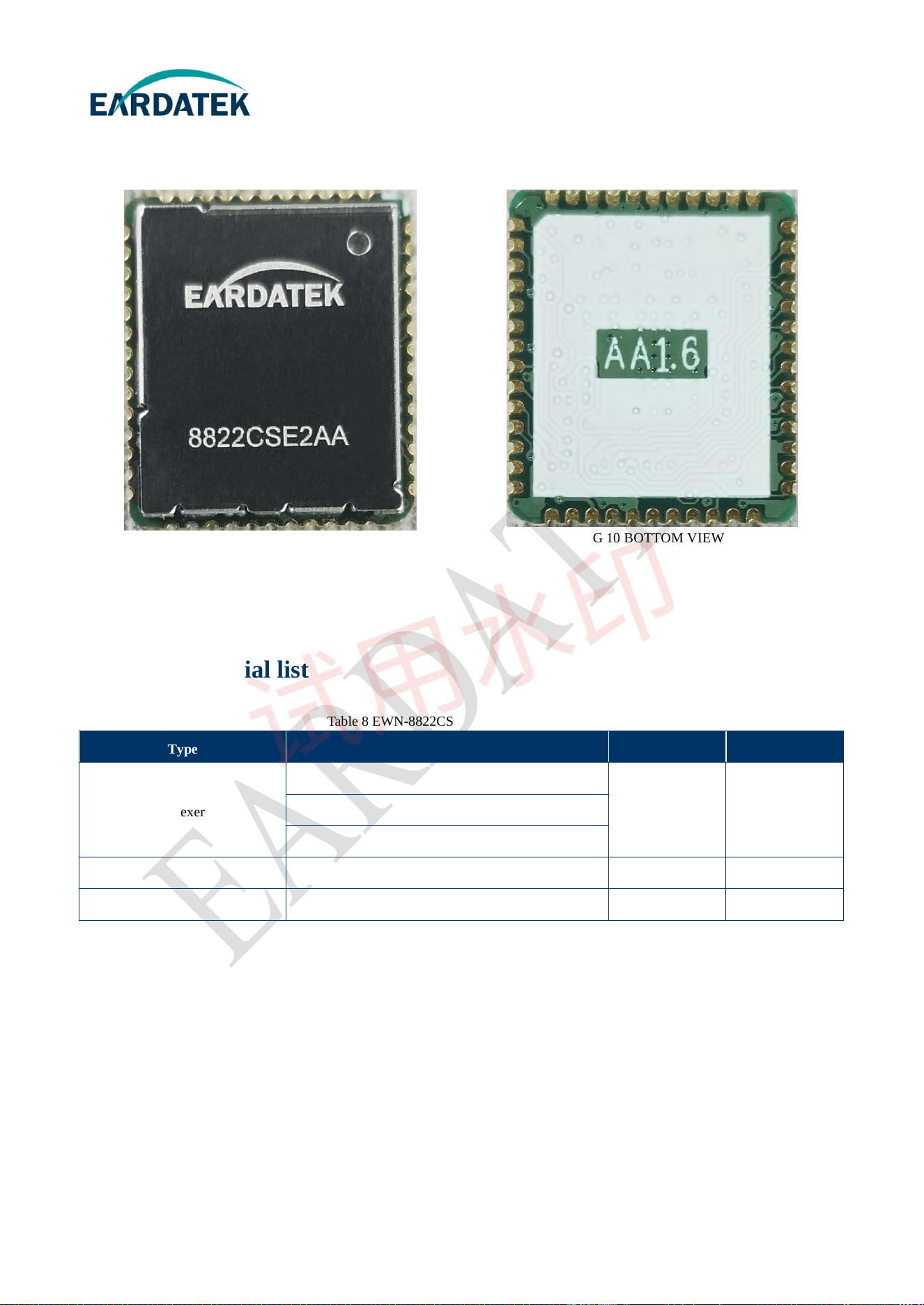
10 Module Photos
FIG 9 TOP VIEW FIG 10 BOTTOM VIEW
11 Key material list
Table 8 EWN-8822CSE2AA Key material list
Type Model Footprint QTY.
Diplexers
LD18D2450LAN-D40/M
1608 2PCS RFDIP1607L132A8D1T
FLT18D24254959D-3288B
IC RTL8822CS-VE-CG QFN76 1 PCS
Crystal 40MHz (CX/YDL/JWT/TJ) X3225 1 PCS
Module:EWN-8822CSE2AA
Waiting for your suggestion at anytime. - 17 - E-mail:sales@eardatek.com
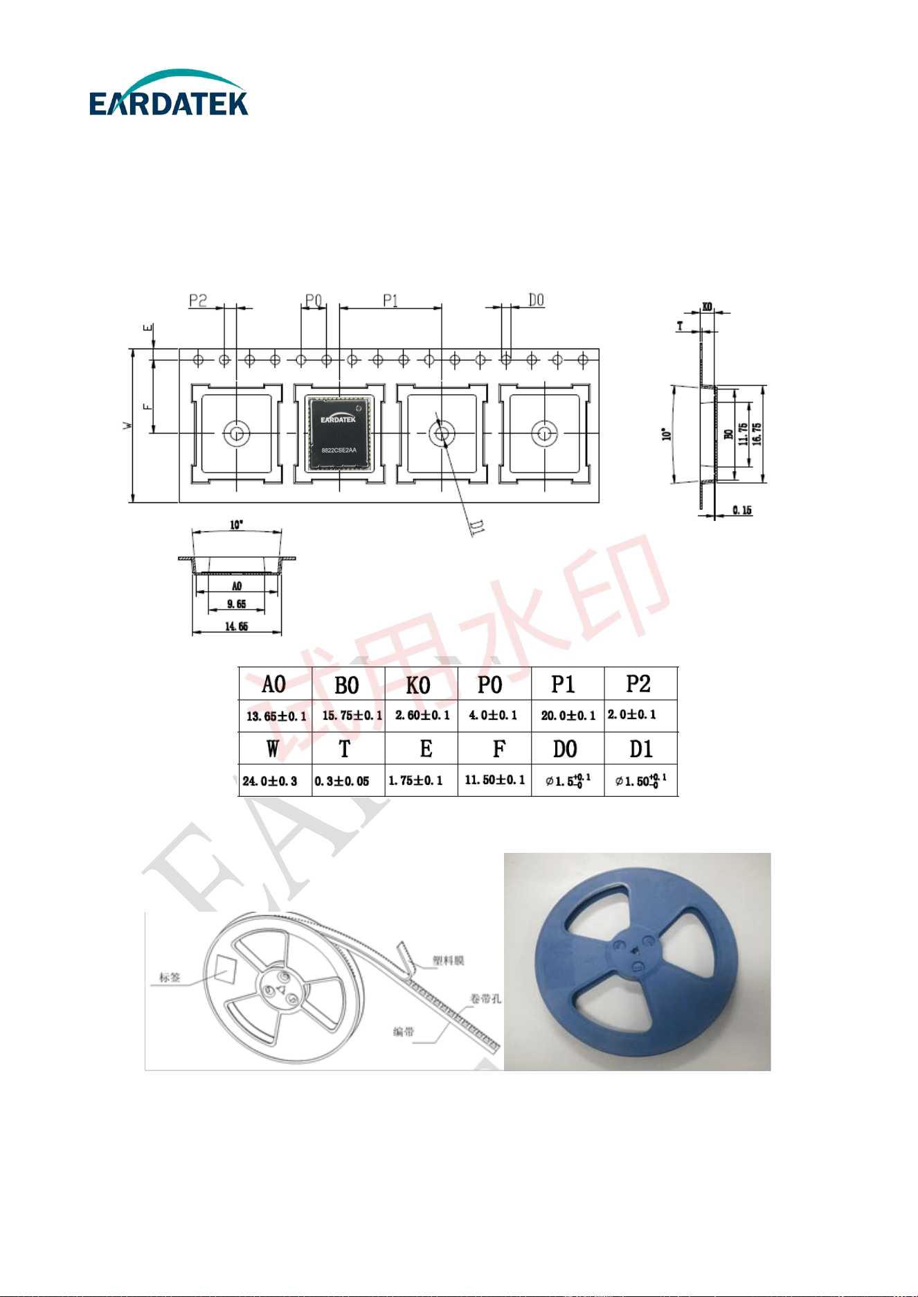
12 Package Information
Carrier dimension: (Unit : mm)
FIG 11 Carrier size
Reel dimension: D=38cm 1400PCS Modules Per Reel
FIG 12 Reel FIG 13 Reel figure
Module:EWN-8822CSE2AA
Waiting for your suggestion at anytime. - 18 - E-mail:sales@eardatek.com
13 Reference design
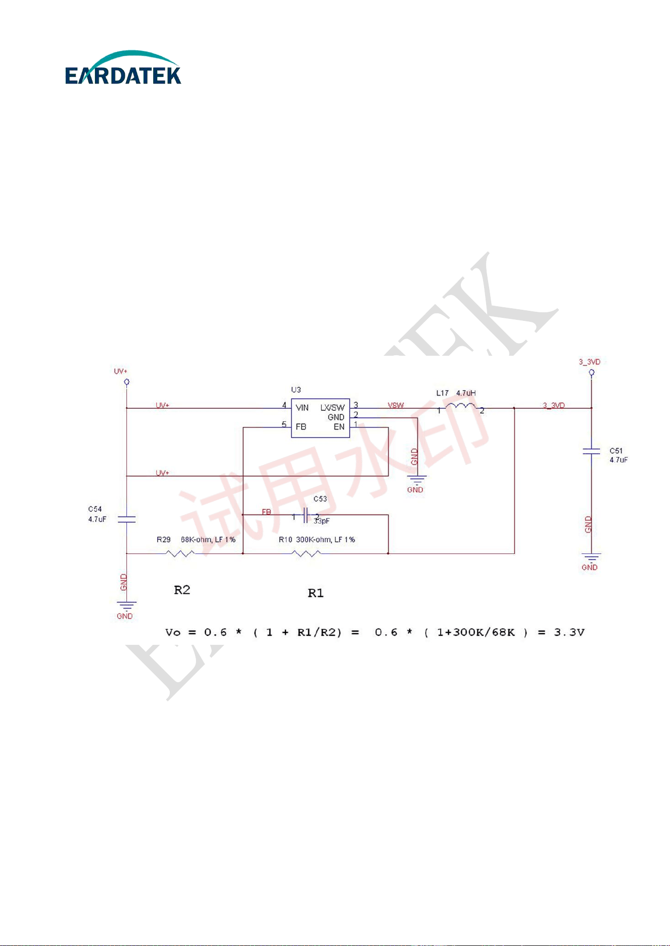
13.1 Power supply requirement
The module power supply voltage is DC+3.3V, and the maximum module current is 1.5A. The power supply
design needs to consider the output current and power interference. To avoid the +3.3V power supply from inter-
fering with other circuits on the motherboard, it is recommended to supply to the module using the regulator cir-
cuit alone. the recommended DC-DC circuit structure shown in the figure below. A 4.7uF~10uF capacitor is con-
nected in parallel at 3_3VD output to filter out the interference. A bead is connected in series at 3_3VD output.
The bead and capacitor must be placed as close to the module as possible. If you need to share +3.3V with other
circuits, consider whether the current of the shared power supply is sufficient.
FIG 14 Power supply Circuit schematic
Module:EWN-8822CSE2AA
Waiting for your suggestion at anytime. - 19 - E-mail:sales@eardatek.com
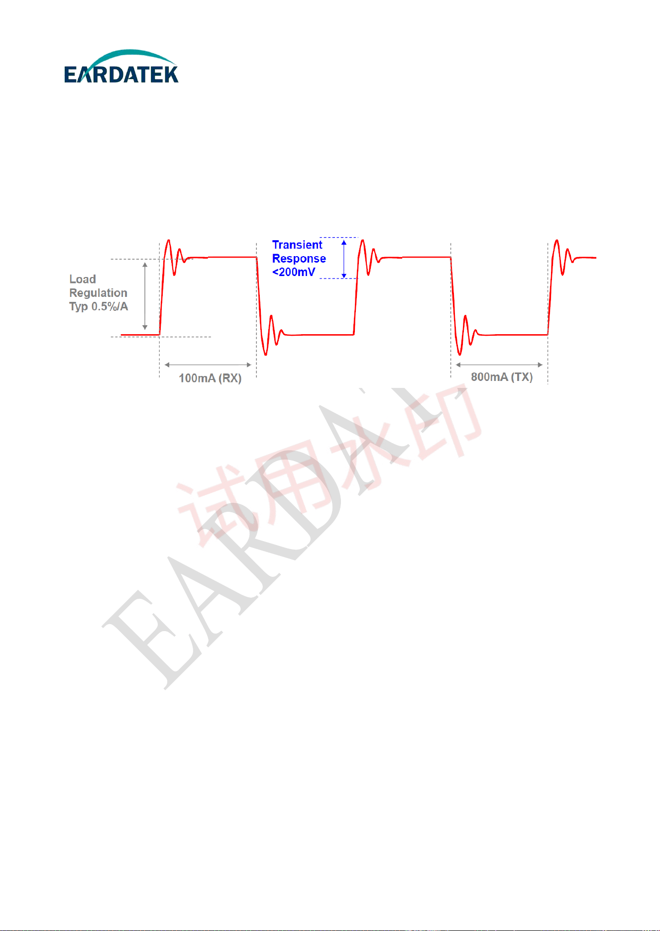
To use a dedicated power supply circuit for Wi-Fi (and BT)
The VD33 power ripple shall be <300mVpp for ripple frequency <200KHz
Transient-response:
①the ripple raised from 100/800mA step-response test should be small than 200mVpp.
②The ripple swing shall settle down within 1~2 cycles,2 cycles for the worst case.
Power supply spur: make sure the spurs from switching mode power supply or other noisy circuits are rea-
sonable small. Once issue concerned with such a power supply spur, alternative power supply filtering might
be needed.
FIG 15 Power supply requirement
Module:EWN-8822CSE2AA
Waiting for your suggestion at anytime. - 20 - E-mail:sales@eardatek.com
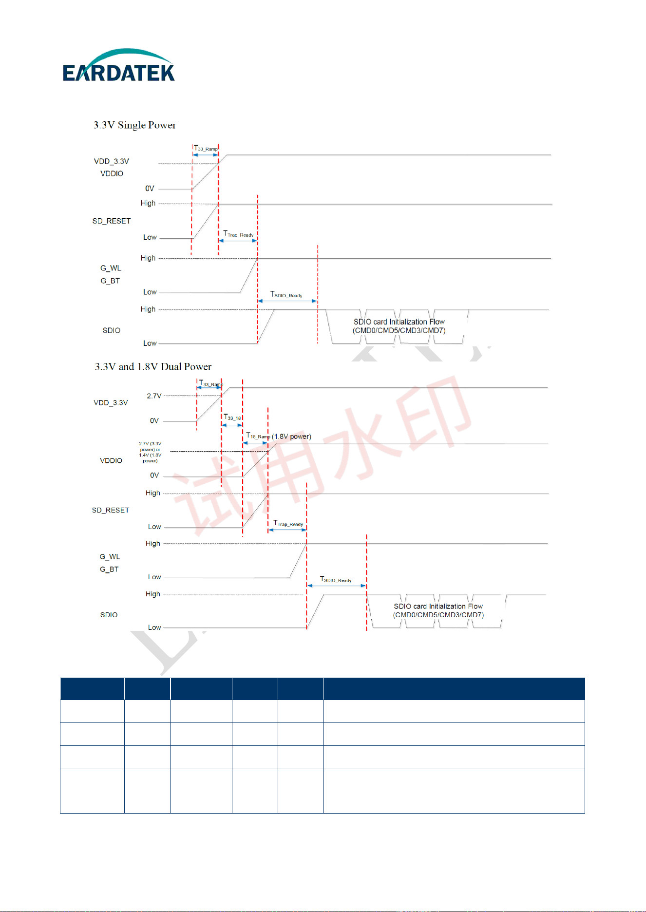
13.2 System power on sequence
FIG 16 System Power On Sequence
Table 9 System Power On Timing Parameters
Symbol Min. Typical Max. Unit Description
T
18_Ramp
/
T
33_Ramp
0.5 1.5 5 ms The 3.3V or 1.8V power ramp up duration.
T
33_18
0 5 - ms
If 1.8V power is applied, it needs to be equal or slower than
3.3V power
T
Trap_Ready
400 500 - ms WLAN eFuse autoload. T
Trap_Ready
= 500ms (Typical)
T
SDIO_ Ready
10 20 100 ms
SDIO Not Ready Duration.
In this state, the module may respond to commands without the
ready bit being set. After the ready bit is set, the host will initi-
ate complete card detection procedure.
Module:EWN-8822CSE2AA
Waiting for your suggestion at anytime. - 21 - E-mail:sales@eardatek.com
13.3 SDIO Interface
The SDIO Bus traces impedance should be 50 Ohm.
The SDIO Bus traces spacing should be more than 2 times of terace width (H=2W)
The SDIO Bus traces (CLK, CMD, D0~D3) length matching szhould be less than +/-100 mils, and the t
otal length should be less than 2.5 inches.
SDIO CLK traces should be surrounded by GND and keep CMD and data away.
The SDIO Bus traces should not have Stubs and need to reference to GND.
The maximum VIA counts of the SDIO Bus traces (CLK, CMD, D0~D3) should less than 4.
The SDIO Bus traces (CLK, CMD, D0~D3) should connect an 0 Ohm series resistor which needs to
close to SOC.
The SDIO Bus traces (CLK, CMD, D0~D3) should reserve pull up resistors 2.2K Ohm to VIO_HOST
which needs to close to WIFI.
The SDIO Bus Traces (CLK, CMD, D0~D3) should reserve 5.6pF caps to GND witch needs to close to
WIFI.
13.4 RF circuit
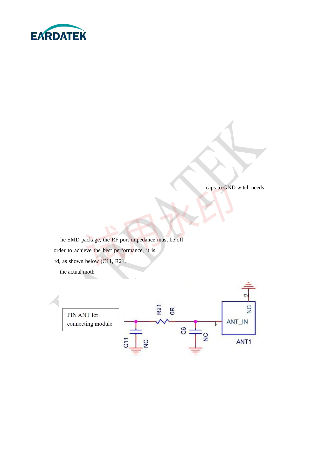
Due to the SMD package, the RF port impedance must be offset after the module is soldered to the mother-
board. In order to achieve the best performance, it is recommended to add a PI-type matching network to the
motherboard, as shown below (C11, R21, C6). The value of the PI type matching network needs to be debugged
according to the actual motherboard to match RF port impedance to 50 Ohm.
FIG 17 Connect 50 Ohm matching antenna reference circuit
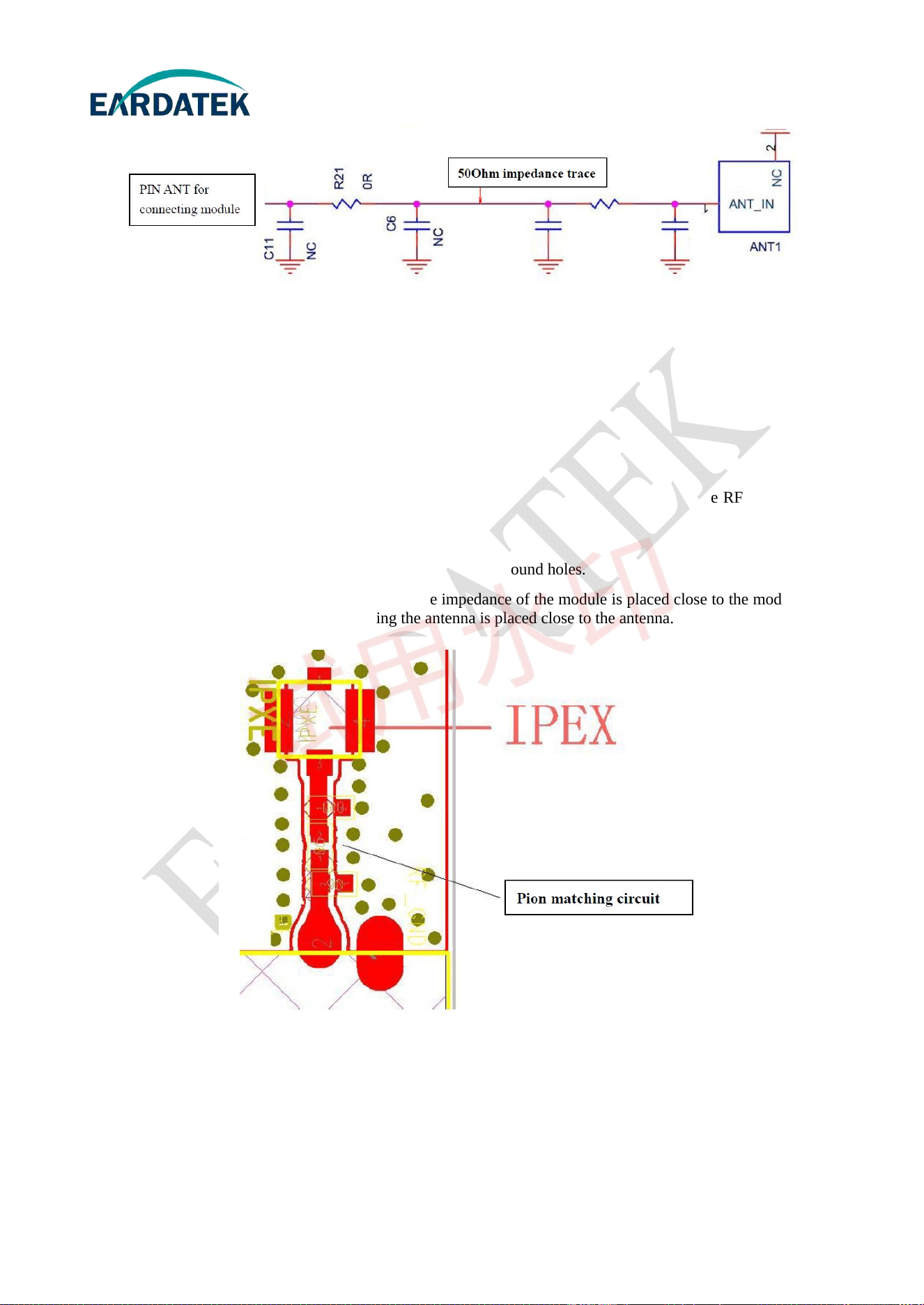
The antenna ANT1 in the figure above must be 50 Ohm. If the antenna is not matched, it is recommended to
add a set of PI type matching network at the front of the antenna to match the antenna. Generally, the antenna
manufacturers will give Suggestions on matching parameters.
Module:EWN-8822CSE2AA
Waiting for your suggestion at anytime. - 22 - E-mail:sales@eardatek.com
FIG 18 Connect the unmatched antenna reference circuit
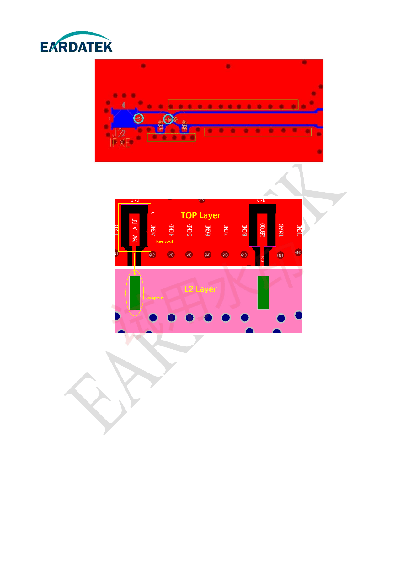
The RF line layout should be matched according to 50ohm. The line impedance is related to the plate, plate
thickness, line width and copper spacing. Professional software can be used to calculate the line width. Note: for
multilayer plates, the plate thickness should calculate the distance from RF routing layer to GND of the next layer.
There are RF lines Layout principles:
1. RF line layout needs to match 50 ohms. The line width can be calculated by professional software. (Note:
If it is a multi-layer board, the board thickness should calculate the distance from the RF trace layer to
the next ground layer.)
2. The RF line must be surrounded by ground copper and ground holes.
3. The PI-type matching circuit for adjusting the impedance of the module is placed close to the module. The
PI type matching circuit for matching the antenna is placed close to the antenna.
FIG 19 The PI type matching circuit Layout
Module:EWN-8822CSE2AA
Waiting for your suggestion at anytime. - 23 - E-mail:sales@eardatek.com
FIG 20 The RF line Layout
4. 4-layer PCB, RF pad must be kept out >= 10mil at the TOP layer, and pads with larger widths(>1.3
times line), the second layer GND needs to be kept out in equal area.
FIG 21 The RF Pads keepout design
Module:EWN-8822CSE2AA
Waiting for your suggestion at anytime. - 24 - E-mail:sales@eardatek.com
13.5 Application Circuit for SD_RESET and BT_DIS_N with Platform
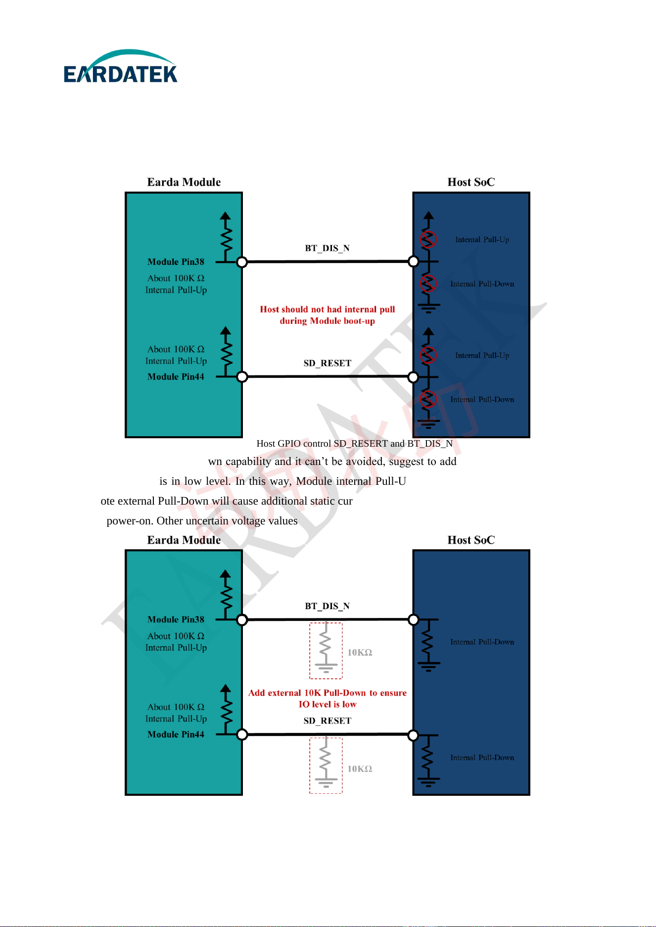
There is internal pull-Up, about 100K, resistor design in BT_DIS_N and SD_RESET. If Host SOC need to
control these two pins, it is recommended to choose host GPIO without pull capability to avoid voltage divider.
Middle range of IO voltage would affect Module booting up (FIG 22).
FIG 22 Host GPIO control SD_RESERT and BT_DIS_N
If Host GPIO has Pull-Down capability and it can’t be avoided, suggest to add 10KΩ Pull-Down resistor in
circuit to ensure IO is in low level. In this way, Module internal Pull-Up 100KΩ could be neglected (FIG 23).
Please note external Pull-Down will cause additional static current. BT_DIS_N exists only high level and low lev-
el during power-on. Other uncertain voltage values may cause BT to fail to open.
FIG 23 Add external pull down resistor to ensure low level

Module:EWN-8822CSE2AA
Waiting for your suggestion at anytime. - 25 - E-mail:sales@eardatek.com
13.6 Motherboard interference avoidance
Motherboard interference comes from: high-speed data interface (HDMI), the Operating frequency of main
chip, DDR, DC-DC power supply. The method of avoiding interference according to the characteristics of various
signals is also different. The main methods of interference avoidance include:
1. keeping away from the source of interference;
2. Adding shields to avoid interference leakage;
3. Reasonable layout to eliminate interference.
13.6.1 Interface interference
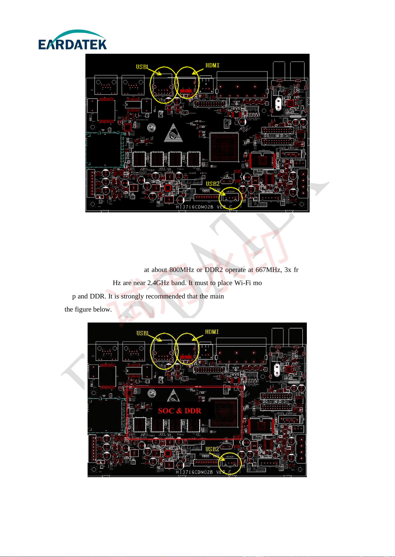
When HDMI uses the 74.2MHz frequency, its 33x frequency is in the 2.4G band of Wi-Fi, which will seri-
ously interfere with the Wi-Fi signal. If the HDMI frequency is 148.5MHz, although the 16x frequency is not in
the Wi-Fi band, the isolation of the frequency is not good, and the Wi-Fi signal will be interfered to some extent.
If the distance between the HDMI interface and the Wi-Fi module on the PCB is less than 5cm, the HDMI output
display will interfere with the Wi-Fi signal, resulting in problems such as Wi-Fi connection failure and throughput
drop. Therefore, keep the location of the Wi-Fi module away from the HDMI port on the hardware layout to avoid
interference.
At the same time, if the Wi-Fi antenna is built-in the motherboard, its placement must also be carefully con-
sidered to be far from the interface interference. If the antenna is placed in an incorrect position, even if the mod-
ule is shielded, the interference signal is coupled through the antenna, which will eventually result in a lower
Wi-Fi throughput. (Note: In addition to interference, the placement of the internal antenna should also evaluate the
effect of the metal interface, motherboard, and housing material on the antenna impedance.)
Module:EWN-8822CSE2AA
Waiting for your suggestion at anytime. - 26 - E-mail:sales@eardatek.com
FIG 24 HDMI and USB interference
13.6.2 The main chip interferes with DDR
Because the main chips operate at about 800MHz or DDR2 operate at 667MHz, 3x frequency of 800MHz
and 4x frequency of 667MHz are near 2.4GHz band. It must to place Wi-Fi modules and antennas far away from
the main chip and DDR. It is strongly recommended that the main chip be isolated from the DDR by a shield. As
shown in the figure below.
FIG 25 Main chip and DDR interference
Module:EWN-8822CSE2AA
Waiting for your suggestion at anytime. - 27 - E-mail:sales@eardatek.com
13.7 Recommended secondary reflux temperature curve
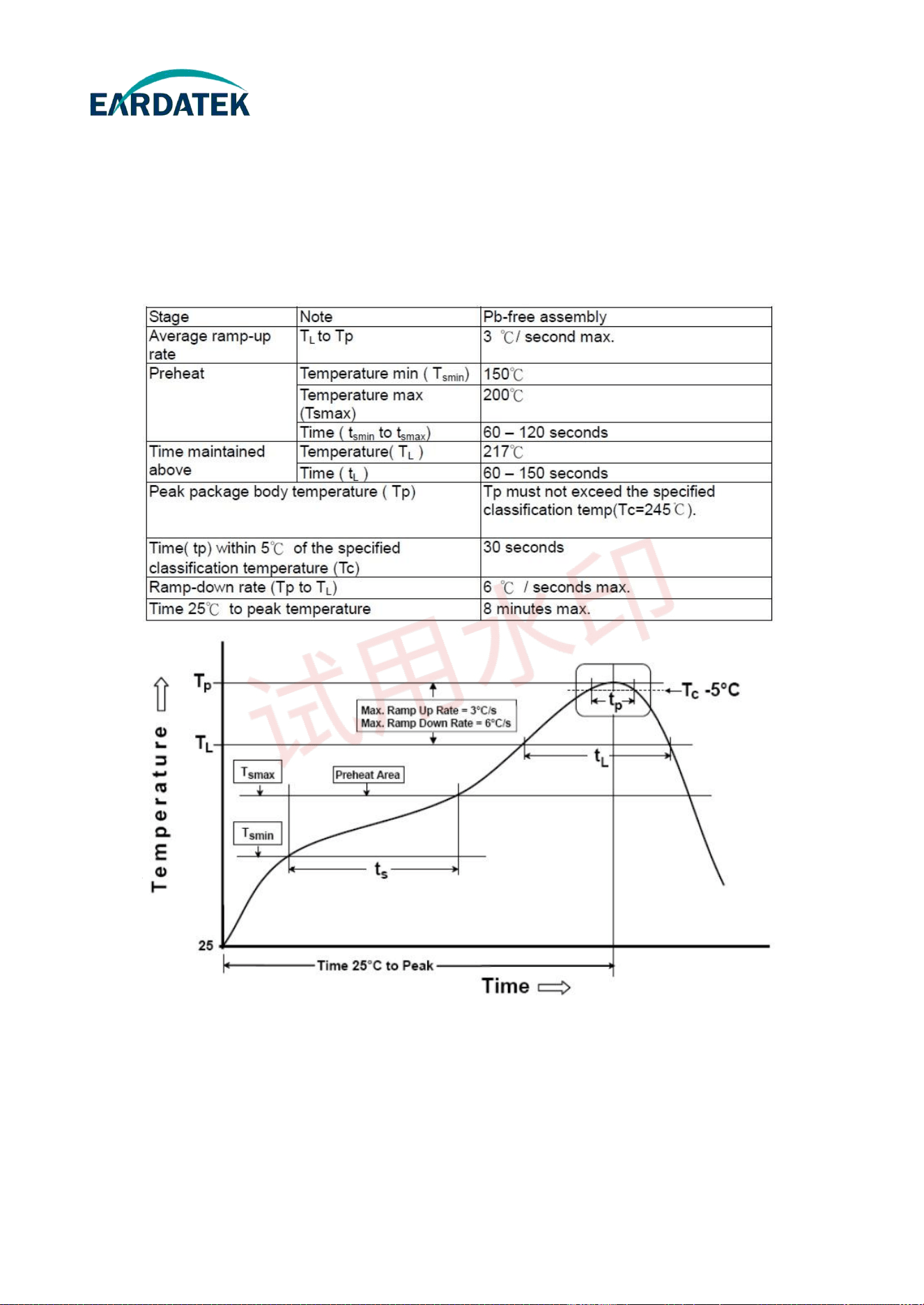
The number of reflux shall not exceed 2 times, and the tin feeding height of the half hole of the module shall
be no less than 1/4.
The lead-free reflux curve requirements of Wi-Fi module products are shown in FIG 26:
FIG 26 Furnace temperature curve
NOTE:
1.The maximum furnace temperature of the module is 260℃, don't exceed this temperature.
2.The gold plating thickness of the module pad is 2u".
Module:EWN-8822CSE2AA
Waiting for your suggestion at anytime. - 28 - E-mail:sales@eardatek.com
14 Revision History
Revision Release Date Summary
Revised By
V1.0
2022-01-26
05-30
First release Jisheng Wang
V1.1
2022-08-01
Update Module Photos
Shuize Wang
V1.2 2022-09-20 Update Wi-Fi Specification
Shuize Wang
V1.3 2022-09-29 Update Wi-Fi Specification
Shuize Wang
V1.4 2023-01-05 Update Key material list Shuize Wang
V1.5 2023-02-02
Update System Block Diagram, Module Photos and Reference de-
sign
Shuize Wang
V1.6 2023-04-23
Update Module Laser Etching Silkscreen, RF Pin Definition, Appli-
cation Circuit for SD_RESET and BT_REG_ON with Platform
Shuize Wang
V1.7 2023-10-10 Update Wi-Fi Specification(Frequency) Shuize Wang
V1.8 2024-11-22
Update System Block Diagram, PHY Specification, DC Characteris-
tics, Pin Definition, Reference design, update peak current parameter
Shuize Wang

NOTE: This equipment has been tested and found to comply with the limits for a Class B digital device, pursuant to part 15 of the FCC Rules.
These limits are designed to provide reasonable protection against harmful interference in a residential installation. This equipment generates,
uses and can radiate radio frequency energy and, if not installed and used in accordance with the instructions, may cause harmful interference
to radio communications. However, there is no guarantee that interference will not occur in a particular installation. If this equipment does
causeharmfulinterferencetoradioortelevisionreception,whichcanbedeterminedbyturningtheequipmentoandon,theuseris
FCC Statement
FCC standards: FCC CFR Title 47 Part 15 Subpart C Section 15.407,15.247
Device is equipped with External antenna, Antenna gain: 2.4G Wi-Fi/BLE/BT:3.98di, 5.2G Wi-Fi:4.39dBi,5.3G Wi-Fi:4.53dBi,
5.6G Wi-Fi:4.81dBi,5.8G Wi-Fi:4.72dBi,
This device complies with part 15 of the FCC Rules. Operation is subject to the following two conditions:
(1) This device may not cause harmful interference, and (2) this device must accept any interference received, including interference that
may causeundesiredoperation.AnyChangesormodificationsnotexpresslyapprovedbythepartyresponsibleforcompliancecouldvoid
the user's authority to operate the equipment.
encouraged to try to correct the interference by one or more of the following measures:
• Reorient or relocate the receiving antenna.
• Increase the separation between the equipment and receiver.
• Connecttheequipmentintoanoutletonacircuitdierentfromthattowhichthereceiverisconnected.
• Consult the dealer or an experienced radio/TV technician for help.
We
willretaincontroloverthenalinstallationofthemodularsuchthatcomplianceoftheendproductisassured.Insuchcases,anoperating
conditiononthelimitmodularapprovalforthemodulemustbeonlyapprovedforusewheninstalledindevicesproducedbyaspecic
manufacturer.IfanyhardwaremodifyorRFcontrolsoftwaremodifywillbemadebyhostmanufacturer,C2PCornewcerticateshouldbe
applytogetapproval,ifthosechangeandmodicationmadebyhostmanufacturernotexpresslyapprovedbythepartyresponsiblefor
compliance ,then it is illegal.
FCC Radiation Exposure Statement
Themodularcanbeinstalledorintegratedinmobileorxdevices.Thismodularcannotbeinstalledinanyportabledeviceifwithoutfurther
certicationsuchasC2PCwithSAR.ThismodularcomplieswithFCCRFradiationexposurelimitssetforthforanuncontrolledenvironment.
This transmitter must not be co-located or operating in conjunction with any other antenna or transmitter. This modular must be installed
and operated with a minimum distance of 20 cm between the radiator and user body.
When the module is installed inside another device, the user manual of the host must contain below warning statements;
1. This device complies with Part 15 of the FCC Rules. Operation is subject to the following two conditions:
(1) This device may not cause harmful interference;
IftheFCCidenticationnumberisnotvisiblewhenthemoduleisinstalledinsideanotherdevice,thentheoutsideofthedeviceintowhich
the module is installed must also display a label referring to the enclosed module. This exterior label can use wording such as the
following: “Contains Transmitter Module FCC ID: 2AMM6-EWN8822CSE2AA Or Contains FCC ID: 2AMM6-EWN8822CSE2AA”
(2) This device must accept any interference received, including interference that may cause undesired operation.
NOTE: This equipment has been tested and found to comply with the limits for a Class B digital device, pursuant to part 15 of the FCC Rules.
These limits are designed to provide reasonable protection against harmful interference in a residential installation. This equipment generates,
uses and can radiate radio frequency energy and, if not installed and used in accordance with the instructions, may cause harmful interference
to radio communications. However, there is no guarantee that interference will not occur in a particular installation. If this equipment does
causeharmfulinterferencetoradioortelevisionreception,whichcanbedeterminedbyturningtheequipmentoandon,theuseris
encouraged to try to correct the interference by one or more of the following measures:
• Reorient or relocate the receiving antenna.
• Increase the separation between the equipment and receiver.
• Connecttheequipmentintoanoutletonacircuitdierentfromthattowhichthereceiverisconnected.
• Consult the dealer or an experienced radio/TV technician for help.

19
Pineapple Datasheet
2. Changesormodicationsnotexpresslyapprovedbythepartyresponsibleforcompliancecouldvoidtheuser’sauthoritytooperate
theequipment.Thedevicesmustbeinstalledandusedinstrictaccordancewiththemanufacturer’sinstructionsasdescribedintheuser
documentation that comes with the product. Any company of the host device which install the modular with limit modular approval should
perform the test of radiated & conducted emission and spurious emission, etc. according to FCC part 15C :
15.407,15.247 ,15B Class B requirement, Only if the test result comply with FCC part 15C : 15.407,15.247 ,15B Class B requirement, then
the host can be sold legally.
IC Compliance Statement
This device complies with Innovation, Science and Economic Development Canada (ISED) licence-exempt RSS standard(s).
Operation is subject to the following two conditions:
1. This device may not cause harmful interference, and
2. This device must accept any interference received, including interference that may cause undesired operation of the device.
Modification Warning
Any changes or modifications not expressly approved by the party responsible for compliance could void the user's authority to
operate this equipment.
RF Radiation Exposure Statement
This equipment complies with IC RSS-102 radiation exposure limits set forth for an uncontrolled environment. This equipment
shall be installed and operated with a minimum distance of 20 cm between the radiator and the human body.
This transmitter must not be co-located or operating in conjunction with any other antenna or transmitter.
Host Integration Note
This module is certified for installation in mobile or fixed devices only. It shall not be installed in portable devices without further
certification (e.g. C2PC with SAR evaluation).
The host manufacturer shall perform additional verification for radiated emissions, conducted emissions and spurious emissions
per ICES-003 and relevant RSS standards to ensure end-product compliance.