V
0.2 - Mar. 2025
TR6S621U1 datasheet
S P E C I F I C A T I O N
TR6S621U1
If one receives this document from Truly Electronics Co., Ltd. (hereinafter referred to as "Truly Electronics"), it indicates that one has agreed
to the following terms. If one does not consent to the following terms, please cease the use of this document.
The copyright of this document is owned by Truly Electronics Co., Ltd., and any rights not explicitly granted herein are reserved. This
document involves the proprietary information of Truly Electronics. Without the prior written permission of Truly Electronics, no entity or
individual may duplicate, disseminate, distribute, utilize or disclose this document, as well as any pictures, tables, data and other
information contained therein.
This product conforms to the design requirements regarding environmental protection and personal safety. The storage, use and disposal
of the product should comply with the requirements stipulated in the product manual, relevant contracts or relevant national laws and
regulations.
The company reserves the right to modify and improve the products described in this manual without prior notification; meanwhile, it
reserves the right to revise or withdraw this manual at any time.
If there is any ambiguity or obscurity in the text of this user manual, please consult the company or the distributor promptly.
Address: North Of The Dong Chong Road,Truly IndustrialArea, Shanwei City,Guangdong Province,China.
Website:https://www.truly.com.hk
TRULY
TRULY
TRULY
TRULY
TRULY
TRULY
TRULY
TRULY
TRULY
TRULY
WIFI/BT Module+5G

V
0.2 - Mar. 2025
Page
2
of 18
TR6S621U1 datasheet
Contents
1. Device Overview ...........................................................................................................................................3
1.1 Descriptions ........................................................................................................................................... 3
1.2 Features ................................................................................................................................................. 3
1.2.1 General Features ............................................................................................................................3
1.2.2 Wi-Fi Key Features .........................................................................................................................3
1.2.3 Bluetooth Key Features .................................................................................................................. 4
1.3 Functional Block Diagram ...................................................................................................................... 5
2. Pin Configuration and Functions .................................................................................................................. 5
2.1 Module Pin Diagram ...............................................................................................................................5
2.2 Pin Functions ......................................................................................................................................... 6
3. Specifications ............................................................................................................................................... 7
3.1 WIFI RF Specifications .......................................................................................................................... 7
3.2 Bluetooth RF Specifications ...................................................................................................................9
4. Application and Implementation ................................................................................................................. 10
4.1 Application Diagram .............................................................................................................................10
4.2 Reference design .................................................................................................................................10
4.3 Power on/off Timing..........................................................................................................................10
5. Mechanical and Package ........................................................................................................................... 15
5.1 Mechanical Size ...................................................................................................................................15
5.2 Recommended Land Pattern ...............................................................................................................15
5.3 Package Information ............................................................................................................................ 16
6. Thermal Reflow .......................................................................................................................................... 17
7. Ordering Information .................................................................................................................................. 18
8. Revision History ..........................................................................................................................................18
TRULY
TRULY
TRULY
TRULY
TRULY
TRULY
TRULY
TRULY
TRULY
TRULY

V
0.2 - Mar. 2025
Page
3
of 18
TR6S621U1 datasheet
1. Device Overview
1.1 Descriptions
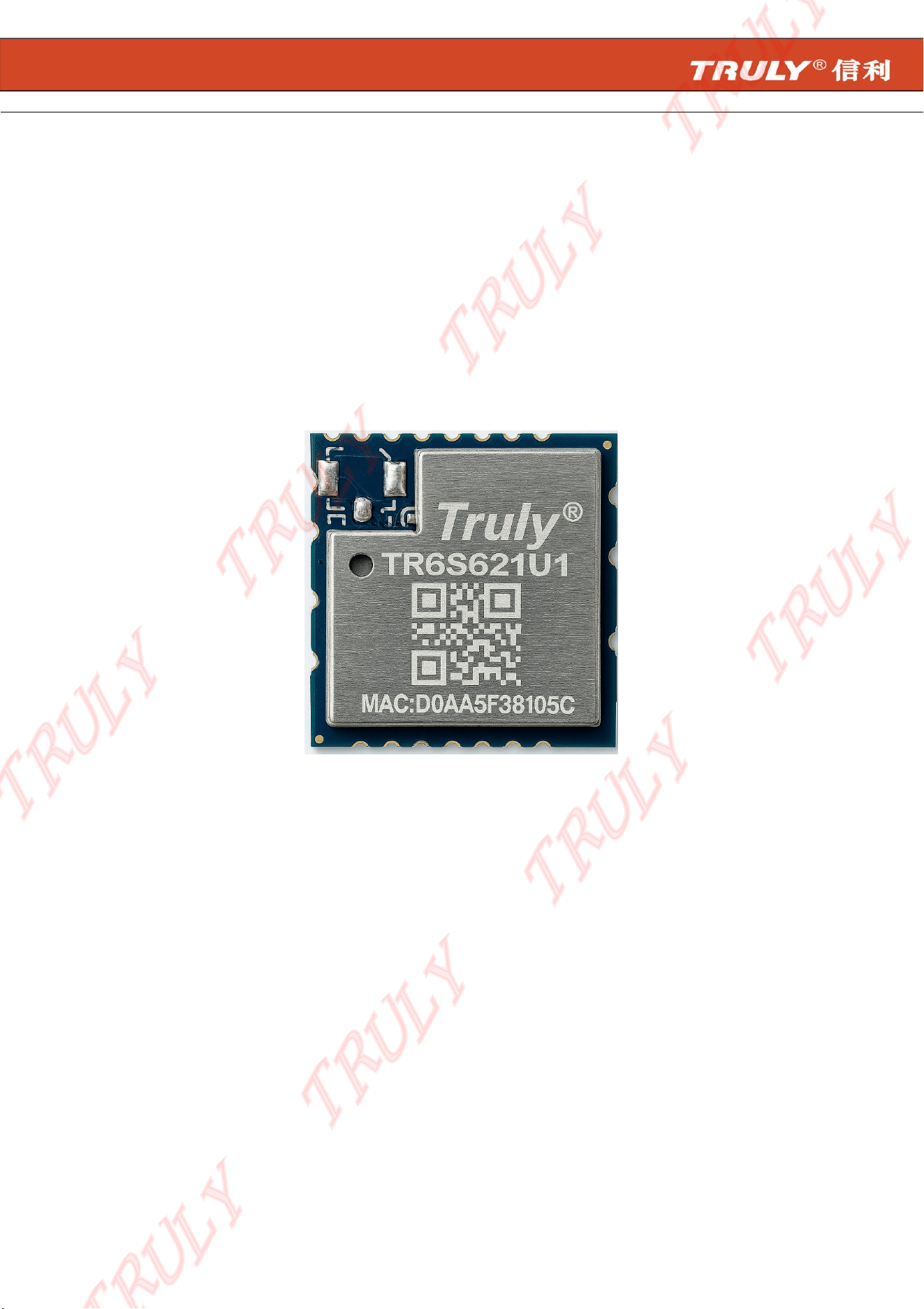
The TR6S621U1 is a highly integrated module that supports 1T1R 802.11 a/b/g/n/ac/ax with Wireless LAN
(WLAN) USB 2.0 interface controller and Bluetooth 5.4 HS-UART interface controller. The high speed
FFT/IFFT paths, combined with BPSK, QPSK, 16QAM, 64QAM、256QAM and up to 1024QAM modulation of
the individual subcarriers, and compatible coding rate of 1/2, 2/3, 3/4, 5/6, provide up to 600.5Mbps for IEEE
802.11ax. The TR6S621U1 MAC supports 802.11e for multimedia applications, 802.11i and WAPI for
security.The TR6S621U1 provides a complete solution for a high-performance integrated wireless and
Bluetooth device.It suitable for STB,TVs,tablets,phones,IPC and other fields such as consumer electronic
devices, and can also be applied to the fields with high reliability requirements,such as industrial
interconnection.
The TR6A621U1 provides a complete solution for a high-performance integrated wireless and Bluetooth
device.
1.2 Features
1.2.1 General Features
Supports 3.3V power supply
Complies with USB 2.0
CMOS MAC, Baseband PHY and RF in a single module for IEEE 802.11a/b/g/n/ac/ax compatible WLAN
IEEE 802.11i (WPA, WPA2, WPA3). Open, shared key, and pair-wise key authentication services
Multiple BSSID feature allows the module to assume multiple MAC identities when used as a wireless
bridge
IEEE 802.11k Radio Resource Measurement
WAPI(Wireless Authentication Privacy Infrastructure) certified
Wi-Fi Direct supports wireless peer to peer application
IEEE802.11h DFS,TPC,Spectrum Measurement
1.2.2 Wi-Fi Key Features
IEEE 802.11a/b/g/n/ac/ax compatible WLAN
Supports IEEE 802.11 d/e/h/i/k/mc/r/v/w
Supports Wi-Fi STA, AP, P2P, TDLS modes
Supports LDPC,STBC
Supports UL/DL OFDMA, DL MU-MIMO
TRULY
TRULY
TRULY
TRULY
TRULY
TRULY
TRULY
TRULY
TRULY
TRULY

V
0.2 - Mar. 2025
Page
4
of 18
TR6S621U1 datasheet
Supports QoS, WFA WMM, WMM PS
Supports WPA, WPA2, WPA3 encryption, WAPI
Supports BSS Color, Spatial Reuse
Supports TWT, Intra-PPDU PS, VHT txop PS
Supports WOW
Supports 2.4Ghz and 5Ghz band channels
20MHz / 40MHz/80MHz Bandwidth transmission
Maximum PHY data rate up to 600.5Mbps in 802.11ax
OFDM with BPSK, QPSK, 16QAM, 64QAM and 256QAM and 1024QAM modulation.
Convolutional Coding Rate: 1/2, 2/3, 3/4, and 5/6
DSSS with DBPSK and DQPSK, CCK modulation with long and short preamble
1.2.3 Bluetooth Key Features
Bluetooth v2.1, v3.0, v4.2, v5.4
HS-UART /USB2.0 as HCI
PCM interface for audio data transmission
Supports VoHCI
Support BR/EDR/LE 1M/LE 2M/LE LR
Support SCO and eSCO link
CVSD/MSBC/PLC
SSP/Secure Connection
Low power mode (sniff, sniff sub-rating)
Supports LE Audio
Supports AOA/AOD
TRULY
TRULY
TRULY
TRULY
TRULY
TRULY
TRULY
TRULY
TRULY
TRULY
V
0.2 - Mar. 2025
Page
5
of 18
TR6S621U1 datasheet
1.3 Functional Block Diagram
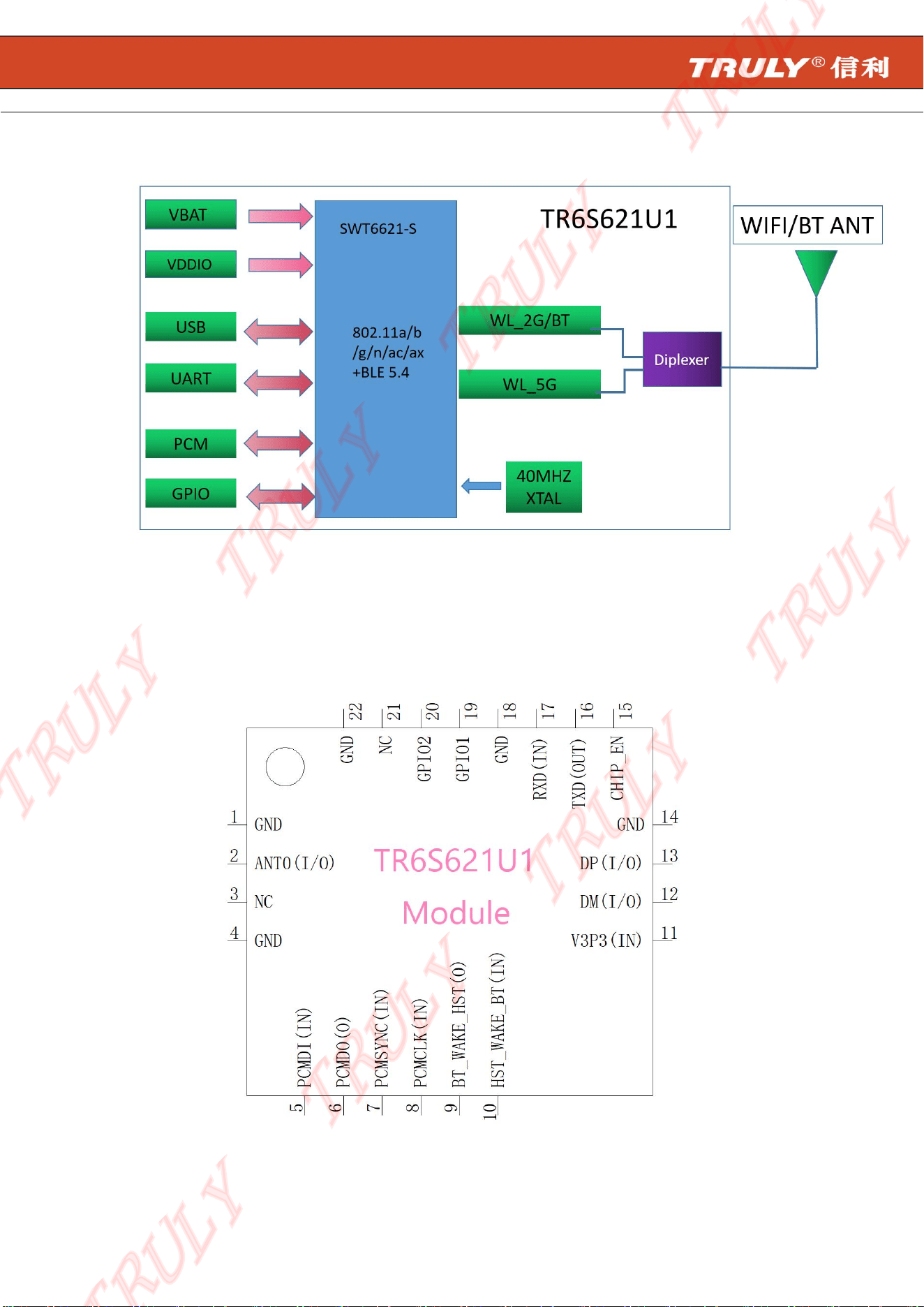
Figure 1. Block Diagram of TR6S621U1
2. Pin Configuration and Functions
2.1 Module Pin Diagram
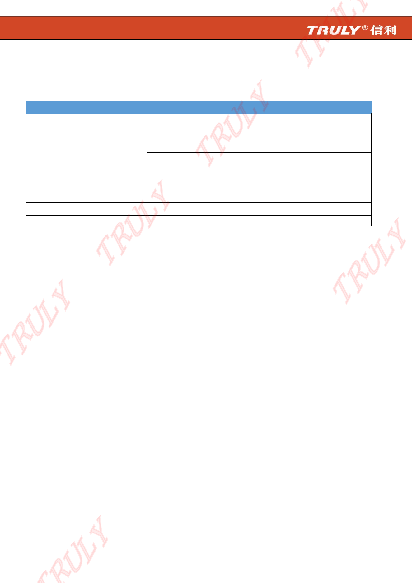
Figure 2.Pin Diagram of TR6S621U1
TRULY
TRULY
TRULY
TRULY
TRULY
TRULY
TRULY
TRULY
TRULY
TRULY

V
0.2 - Mar. 2025
Page
6
of 18
TR6S621U1 datasheet
2.2 Pin Functions
Pin Name
Description
1 GND Ground
2 ANT WLAN and BT RF input/output port
3 NC No connect, keep floating
4 GND Ground
5 PCM_IN PCM data input
6 PCM_OUT PCM data output
7 PCM_SYNC PCM sync signal
8 PCM_CLK PCM clock
9 BT_WAKE_HOST BT wake up Host
10 HOST_WAKE_BT Host wake up BT
11 VBAT 3.3V power supply
12 DM USB Data Minus
13 DP USB Data Positive
15 CHIP_EN Chip Enable pin(high enable/ low disable)
16 TXD High-Speed UART1 TX
17 RXD High-Speed UART1 RX
18 GND Ground
19 GPIO1 GPIO1
20 GPIO2 GPIO2
21 NC No connect, keep floating
22 GND Ground
TRULY
TRULY
TRULY
TRULY
TRULY
TRULY
TRULY
TRULY
TRULY
TRULY
V
0.2 - Mar. 2025
Page
7
of 18
TR6S621U1 datasheet
3. Specifications
3.1 WIFI RF Specifications
Category Descriptions
Dimension L*W*H :13.0mm (±0.2mm)*12.2mm (±0.2mm)*2.0mm (±0.1mm)
Standard IEEE 802.11a/b/g/n/ac/ax+BT 5.4
Frequency Band
2.4GHZ Band: 2412~2500MHZ
5GHZ Band: 5150~5250MHZ@Band1
5250~5350MHZ@Band2
5470~5725MHZ@Band3
5725~5850MHZ@Band4
Bandwidth 20/40/80MHz
Data Security WEP,WPA/WPA2/WPA3
TRULY
TRULY
TRULY
TRULY
TRULY
TRULY
TRULY
TRULY

V
0.2 - Mar. 2025
Page
8
of 18
TR6S621U1 datasheet
Data Rate
802.11b [11,5.5,2 and 1Mbps]
802.11g [54,48,36,24,18,12,9&6Mbps]
802.11n HT20:up to 72.2Mbps
802.11n HT40:up to 150Mbps
802.11ac VHT40:up to 200Mbps
802.11ax HE20:up to 143.4Mbps
802.11ax HE40:up to 286.8Mbps
802.11ax HE80:up to 600.5Mbps
Ambient Temperature -30℃~70℃
Storage Temperature -40℃~85℃
Antenna External RF antenna
Operating System Linux /Android
Operating Voltage VBAT:3.3V;VDDIO:1.8V or 3.3V
TRULY
TRULY
TRULY
TRULY
TRULY
TRULY
TRULY
TRULY
V
0.2 - Mar. 2025
Page
9
of 18
TR6S621U1 datasheet
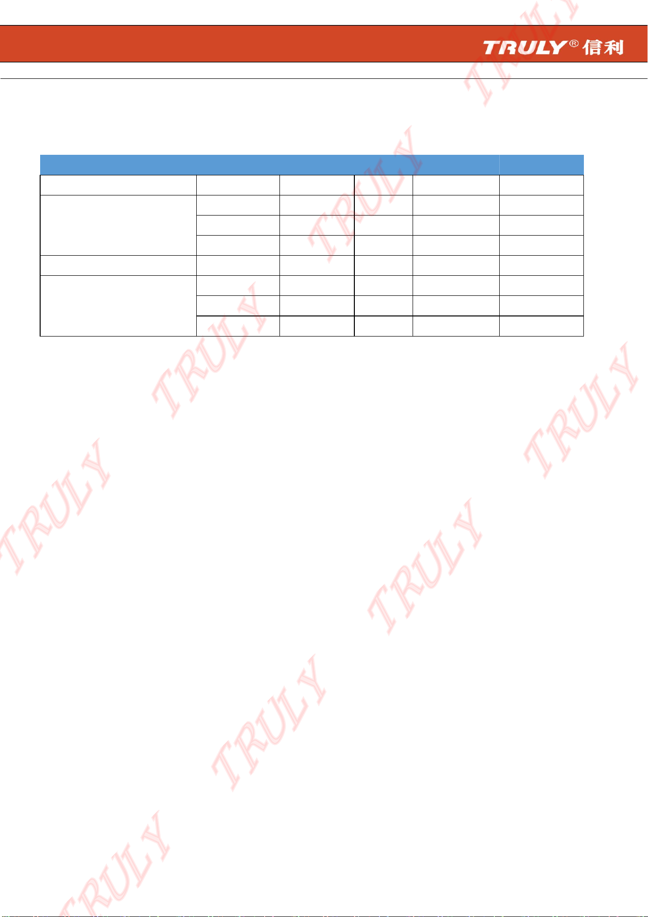
3.2 Bluetooth RF Specifications
Parameter Conditions Minimum Typical Maximum Unit
Frequency range 2402 2480 MHz
RX sensitivity
1 Mbps - -91 - dBm
2 Mbps - -89 - dBm
3 Mbps - -87 - dBm
Initial carrier frequency offset -24 5 24 KHz
Output power
BR 6 8 10 dBm
EDR 4 6 8 dBm
LE 4 6 8 dBm
TRULY
TRULY
TRULY
TRULY
TRULY
TRULY
TRULY
TRULY
TRULY
TRULY
V
0.2 - Mar. 2025
Page
10
of 18
TR6S621U1 datasheet
4. Application and Implementation
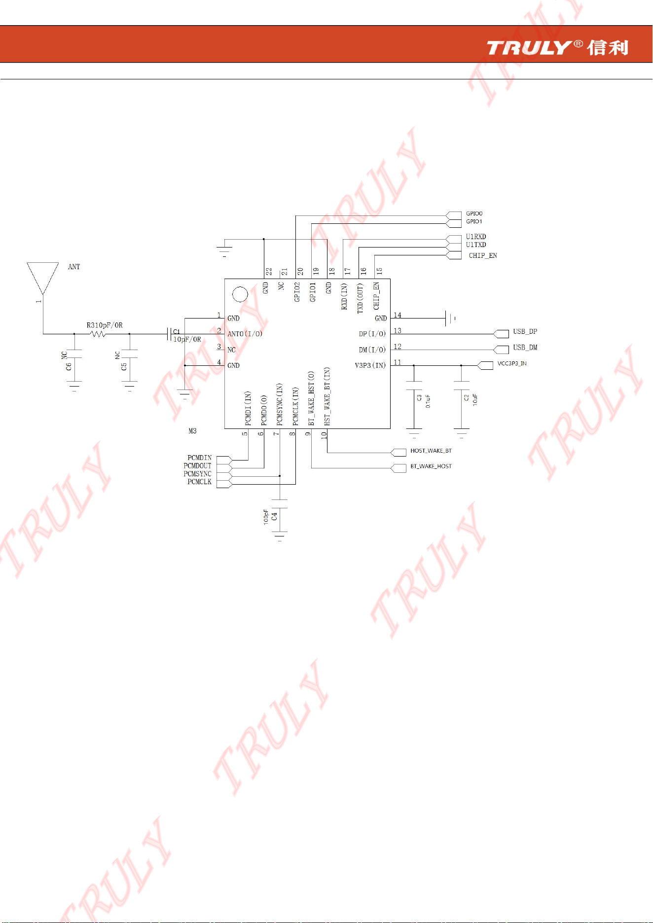
4.1 Application Diagram
Figure 3. Application Schematic Diagram of TR6S621U1
TRULY
TRULY
TRULY
TRULY
TRULY
TRULY
TRULY
TRULY
TRULY
TRULY
V
0.2 - Mar. 2025
Page
11
of 18
TR6S621U1 datasheet
4.2 Reference design
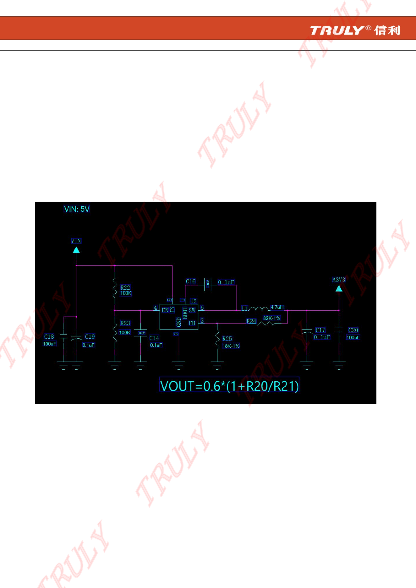
4.2.1 Power supply requirement
The module power supply voltage is DC+3.3V, and the maximum module current is 800mA. The power
supply design needs to consider the output current and power interference. To avoid the +3.3V power supply
from interfering with other circuits on the motherboard, it is recommended to supply to the module using the
regulator circuit alone. the recommended DC-DC circuit structure shown in the figure below. A 4.7uF~10uF
capacitor is connected in parallel at 3_3VD output to filter out the interference. A bead is connected in series at
3_3VD output. The bead and capacitor must be placed as close to the module as possible. If you need to share
+3.3V with other circuits, consider whether the current of the shared power supply is sufficient.
4.2.2 USB Interface
Place the USB PHY as close as possible to the USB 2.0 connector. The signal swing during high-speed
operation on the DP/DM lines is relatively small (400 mV ± 10%), so any differential noise picked up on
the twisted pair can affect the received signal. When the DP/DM traces do not have any shielding, the
traces tend to behave like an antenna and picks up noise generated by the surrounding components in
the environment. To minimize the effect of this behavior:
•
DP/DM traces should always be matched lengths and must be no more than 4 inches in length;
otherwise, the eye opening may be degraded
TRULY
TRULY
TRULY
TRULY
TRULY
TRULY
TRULY
TRULY
TRULY
TRULY
V
0.2 - Mar. 2025
Page
12
of 18
TR6S621U1 datasheet
•
Route DP/DM traces close together for noise rejection on differential signals, parallel to each other and
within two mils in length of each other (start the measurement at the chip package boundary, not to the
balls or pins).
•
A high-speed USB connection is made through a shielded, twisted pair cable with a differential
characteristic impedance of 90 Ω ±15%. In layout, the impedance of DP and DM should each be 45 Ω
± 10%.
•
DP/DM traces should not have any extra components to maintain signal integrity. For example, traces
cannot be routed to two USB connectors.
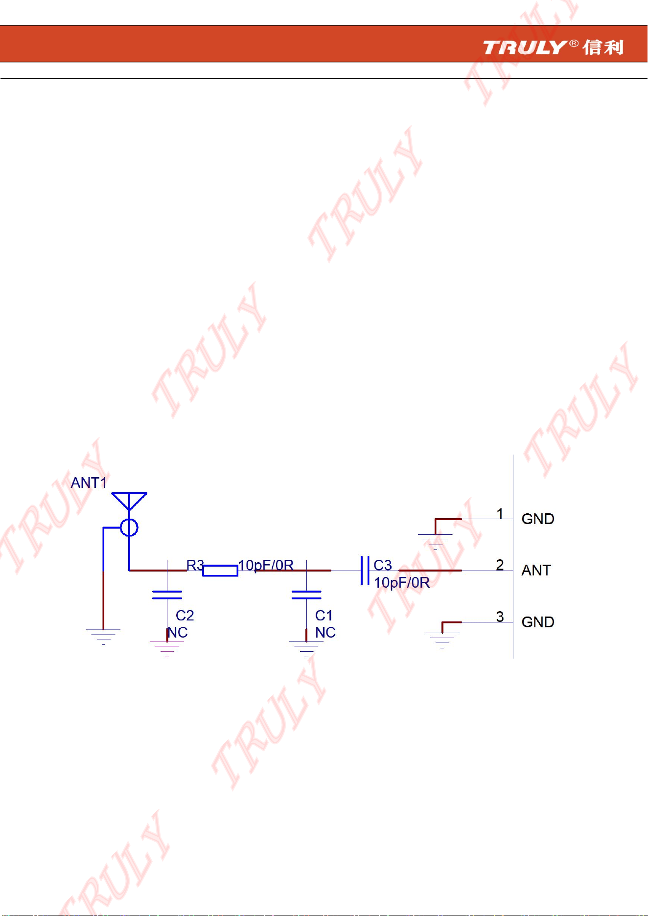
4.2.3 RF circuit
Due to the SMD package, the RF port impedance must be offset after the module is soldered
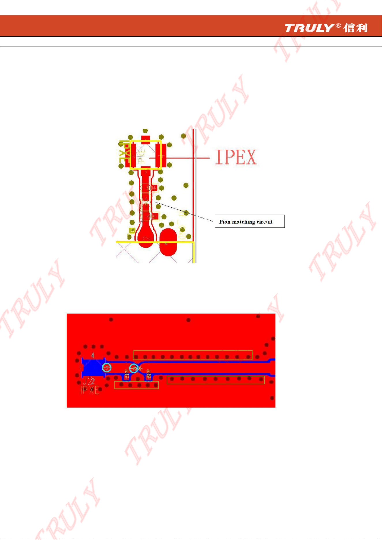
to the motherboard. In order to achieve the best performance,, it is recommended to add a
PI-type matching network to the motherboard, as shown below (C2, R3,C1). The value of the PI
type matching network needs to be debugged according to the actual motherboard to match RF
port impedance to 50 Ohm.
The antenna ANT1 in the figure above must be 50 Ohm. If the antenna is not matched, it is
recommended to add a set of PI type matching network at the front of the antenna to match the
antenna. Generally, the antenna manufacturers will give Suggestions on matching parameters.
The RF line layout should be matched according to 50ohm. The line impedance is related to the
plate, plate thickness, line width and copper spacing. Professional software can be used to alculate
the line width. Note: for multilayer plates, the plate thickness should calculate thedistance from RF
routing layer to GND of the next layer. There are RF lines Layout principles :
a. RF line layout needs to match 50 ohms. The line width can be calculated by professional
TRULY
TRULY
TRULY
TRULY
TRULY
TRULY
TRULY
TRULY
TRULY
TRULY
V
0.2 - Mar. 2025
Page
13
of 18
TR6S621U1 datasheet
software. (Note: If it is a multi-layer board, The board thickness should calculate the distance
from the RF trace layer to the next ground layer.)
b. The RF line must be surrounded by ground copper and ground holes.
c. The PI-type matching circuit for adjusting the impedance of the module is placed close to
the module. The PI type matching circuit for matching the antenna is placed close to the antenna.
The PI type matching circuit Layout
The RF line Layout
TRULY
TRULY
TRULY
TRULY
TRULY
TRULY
TRULY
TRULY
TRULY
TRULY
V
0.2 - Mar. 2025
Page
14
of 18
TR6S621U1 datasheet
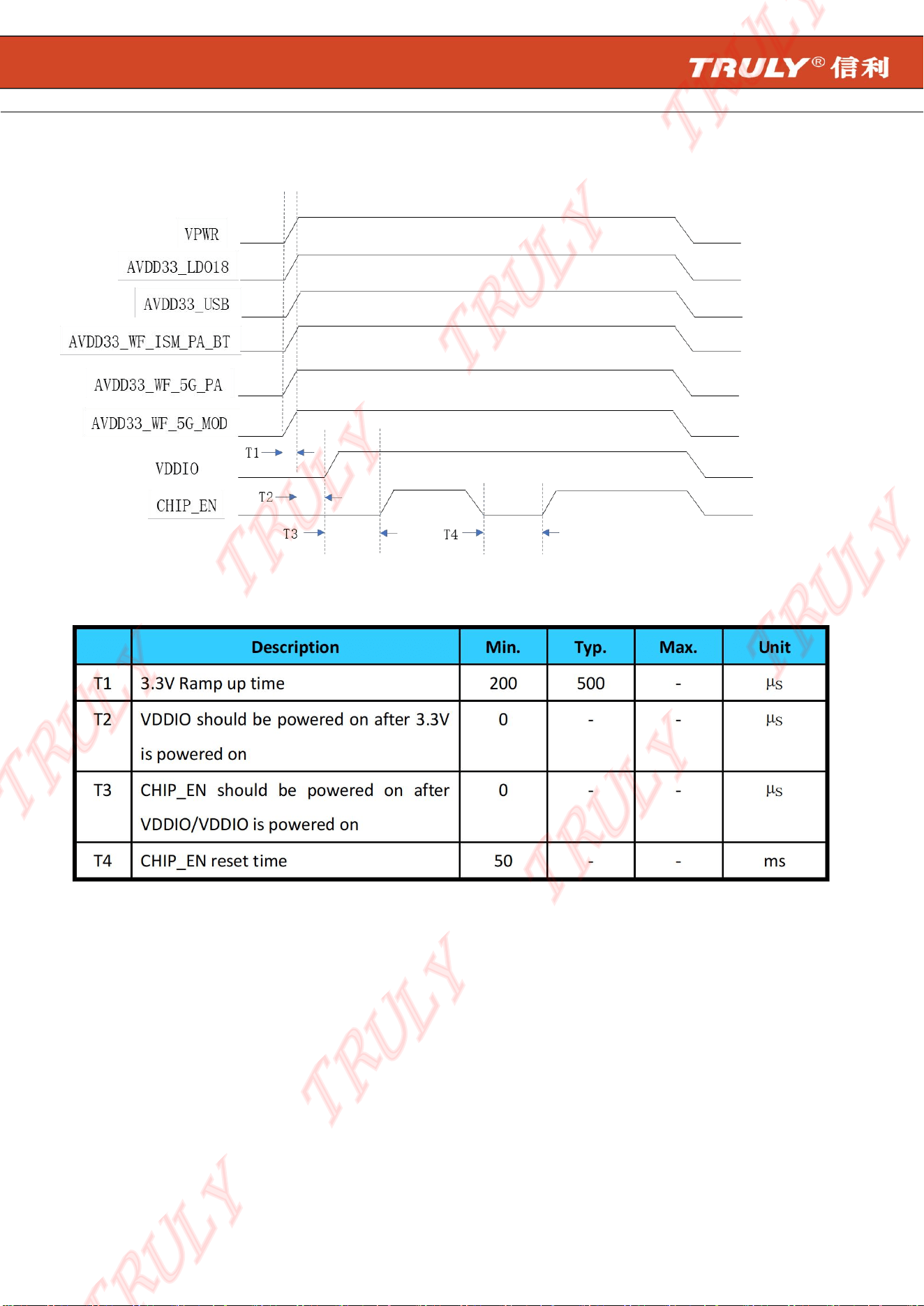
4.3 Power on/off Timing
The figure below shows the chip power on sequence.
TRULY
TRULY
TRULY
TRULY
TRULY
TRULY
TRULY
TRULY
TRULY
TRULY
V
0.2 - Mar. 2025
Page
15
of 18
TR6S621U1 datasheet
5. Mechanical and Package
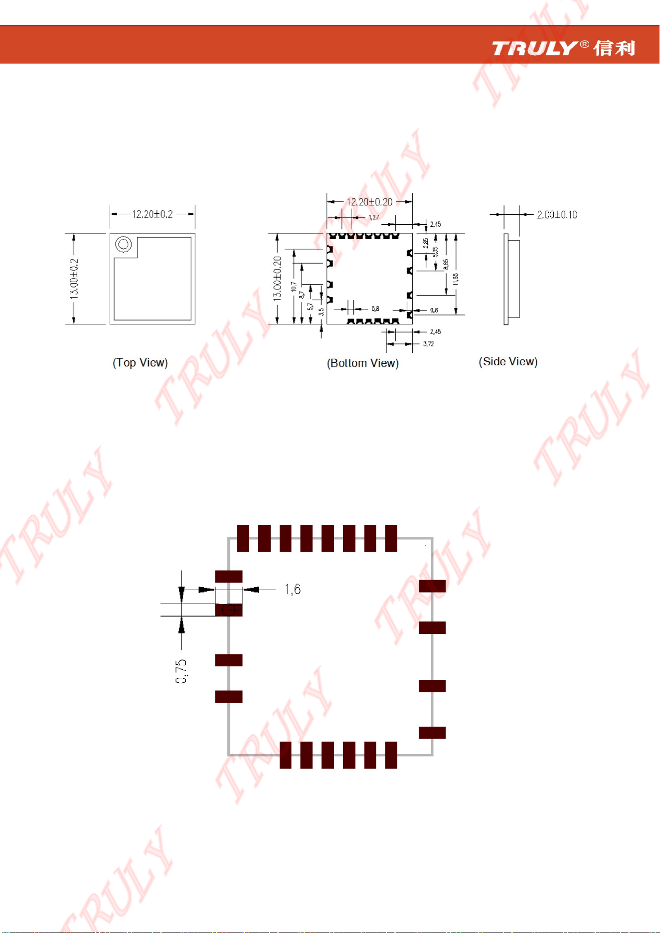
5.1 Mechanical Size
Note:L*W*H: 13.0mm (±0.2mm)*12.2mm (±0.2mm)*2.2mm (±0.1mm)
Figure 4. Mechanical Size of TR6S621U1
5.2 Recommended Land Pattern
Figure 5. On Board Pad Suggest: (Unit: mm)
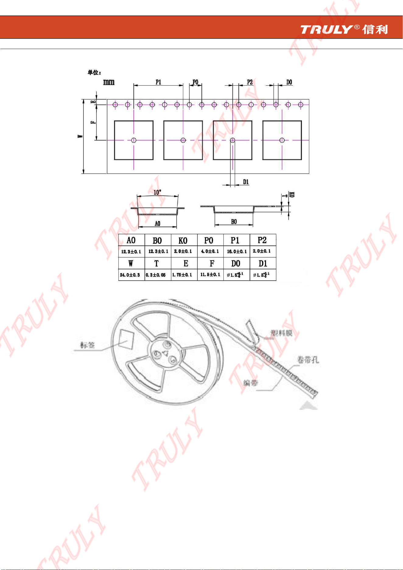
5.3 Package Information
TRULY
TRULY
TRULY
TRULY
TRULY
TRULY
TRULY
TRULY
TRULY
TRULY
V
0.2 - Mar. 2025
Page
16
of 18
TR6S621U1 datasheet
Figure 6. Brief Packaging Process of TR6S621U1 Modules
6. Thermal Reflow
TRULY
TRULY
TRULY
TRULY
TRULY
TRULY
TRULY
TRULY
TRULY
TRULY

V
0.2 - Mar. 2025
Page
17
of 18
TR6S621U1 datasheet
The number of reflux shall not exceed 2 times, and the tin feeding height of the half hole of
the module shall be no less than 1/4.
Figure 7. Recommended Reflow for Lead Free Solder
Note: The module is recommended not to go through reflow oven twice.
TRULY
TRULY
TRULY
TRULY
TRULY
TRULY
TRULY
TRULY
TRULY
TRULY

V
0.2 - Mar. 2025
Page
18
of 18
TR6S621U1 datasheet
7. Ordering Information
8. Revision History
Part NO. Working Voltage ANT Shielding Cover Remark
TR6S621U1 3.3V 1 antennas Included USB
Version Change Content Reviser Date
V0.1 Draft Version Grant 2024.06.08
V0.2 Change Application Diagram Grant 2025.03.08
TRULY
TRULY
TRULY
TRULY
TRULY
TRULY
TRULY
TRULY
TRULY
TRULY

FCC Statement
This device complies with part 15 of the FCC Rules. Operation is subject to the following two
conditions:
(1) This device may not cause harmful interference, and
(2) this device must accept any interference received, including interference that may cause undesired
operation.
Any Changes or modifications not expressly approved by the party responsible for compliance could void
the user's authority to operate the equipment.
The modular can be installed or integrated in mobile or fix devices only. This modular cannot be
installed in any portable device.
Any company of the host which install this modular with Single modular approval should perform the test
of radiated emissionand spurious emission according to FCC part 15C : 15.247 and 15.209 requirement,
Only if the test result comply with FCC part 15C : 15.247 and 15.209 requirement, then the host can be
sold legally.
FCC Radiation Exposure Statement
This modular complies with FCC RF radiation exposure limits set forth for an uncontrolled
environment. This transmitter must not be co-located or operating in conjunction with any other
antenna or transmitter. This modular must be installed and operated with a minimum distance of 20 cm between
the radiator and user body.
Note: This equipment has been tested and found to comply with the limits for a Class B digital
device, pursuant to part 15 of the FCC Rules. These limits are designed to provide reasonable
protection against harmful interference in a residential installation. This equipment generates
uses and can radiate radio frequency energy and, if not installed and used in accordance with the
instructions, may cause harmful interference to radio communications. However, there is no
guarantee that interference will not occur in a particular installation. If this equipment does
cause harmful interference to radio or television reception, which can be determined by turning
the equipment off and on, the user is encouraged to try to correct the interference by one or
more of the following measures:
-Reorient or relocate the receiving antenna.
-Increase the separation between the equipment and receiver.
-Connect the equipment into an outlet on a circuit different from that to which the receiver is
connected.
-Consult the dealer or an experienced radio/TV technician for help.

OEM INTEGRATION INSTRUCTIONS:
This device is intended only for OEM integrators under the following conditions:
The module must be installed in the host equipment such that 20 cm is maintained between the antenna
and users, and the transmitter module may not be co-located with any other transmitter or antenna. The
module shall be only used with the internal on-board antenna that has been originally tested and certified
with this module. External antennas are not supported. As long as these 3 conditions above are met,
further transmitter test will not be required.
However, the OEM integrator is still responsible for testing their end-product for any additional compliance
requirements required with this module installed (for example, digital device emissions, PC peripheral
requirements, etc.). The end-product may need Verification testing, Declaration of Conformity testing, a
Permissive Class II Change or new Certification. Please involve a FCC certification specialist in order to
determine what will be exactly applicable for the end-product.
Validity of using the module certification:
In the event that these conditions cannot be met (for example certain laptop configurations or co-location
with another transmitter), then the FCC/IC authorization for this module in combination with the host
equipment is no longer considered valid and the FCC ID/IC of the module cannot be used on the final
product. In these circumstances, the OEM integrator will be responsible for re-evaluating the end product
(including the transmitter) and obtaining a separate FCC authorization. In such cases, please involve a
FCC/IC certification specialist in order to determine if a Permissive Class II Change or new Certification is
required.
Upgrade Firmware:
The software provided for firmware upgrade will not be capable to affect any RF parameters as certified
for the FCC/IC for this module, in order to prevent compliance issues.
End product labeling:
This transmitter module is authorized only for use in device where the antenna may be installed such that
20 cm may be maintained between the antenna and users. The final end product must be labeled in a
visible area with the following: “Contains FCC ID: 2BOHY-621U1”.
Information that must be placed in the end user manual:
The OEM integrator has to be aware not to provide information to the end user regarding how to install
or remove this RF module in the user's manual of the end product which integrates this module. The end
user manual shall include all required regulatory information/warning as show in this manual.
2.2 List of applicable FCC rules
List the FCC rules that are applicable to the modular transmitter. These are the rules that specifically
establish the bands of operation, the power, spurious emissions, and operating fundamental frequencies.

DO NOT list compliance to unintentional-radiator rules (Part 15 Subpart B/ICES-003) since that is not a
condition of a module grant that is extended to a host manufacturer. See also Section 2.10 below
concerning the need to notify host manufacturers that further testing is required.
Explanation: This module meets the requirements of FCC part 15C(15.247), FCC part 15E(15.407).
2.3 Summarize the specific operational use conditions
Describe use conditions that are applicable to the modular transmitter, including for example any limits
on antennas, etc. For example, if point-to-point antennas are used that require reduction in power or
compensation for cable loss, then this information must be in the instructions. If the use condition
limitations extend to professional users, then instructions must state that this information also extends
to the host manufacturer’s instruction manual. In addition, certain information may also be needed, such
as peak gain per frequency band and minimum gain, specifically for master devices in 5 GHz DFS bands.
Explanation: The EUT antenna is dipole antenna.
2.4 Limited module procedures
If a modular transmitter is approved as a “limited module,” then the module manufacturer is responsible
for approving the host environment that the limited module is used with. The manufacturer of a limited
module must describe, both in the filing and in the installation instructions, the alternative means that
the limited module manufacturer uses to verify that the host meets the necessary requirements to
satisfy the module limiting conditions.
A limited module manufacturer has the flexibility to define its alternative method to address the
conditions that limit the initial approval, such as: shielding, minimum signaling amplitude, buffered
modulation/data inputs, or power supply regulation. The alternative method could include that the
limited module manufacturer reviews detailed test data or host designs prior to giving the host
manufacturer approval.
This limited module procedure is also applicable for RF exposure evaluation when it is necessary to
demonstrate compliance in a specific host. The module manufacturer must state how control of the
product into which the modular transmitter will be installed will be maintained such that full
compliance of the product is always ensured. For additional hosts other than the specific host
originally granted with a limited module, a Class II permissive change is required on the module grant
to register the additional host as a specific host also approved with the module.
Explanation: The Module is not a limited module.
2.5 Trace antenna designs
For a modular transmitter with trace antenna designs, see the guidance in Question 11 of KDB
Publication 996369 D02 FAQ – Modules for Micro-Strip Antennas and traces. The integration information
shall include for the TCB review the integration instructions for the following aspects: layout of trace
design, parts list (BOM), antenna, connectors, and isolation requirements.
a) Information that includes permitted variances (e.g., trace boundary limits, thickness, length,
width, shape(s),
dielectric constant, and impedance as applicable for each type of antenna);
b) Each design shall be considered a different type (e.g., antenna length in multiple(s) of frequency,the
wavelength, and antenna shape (traces in phase) can affect antenna gain and must be considered); c)
The parameters shall be provided in a manner permitting host manufacturers to design the printed
circuit (PC) board layout;
d) Appropriate parts by manufacturer and specifications;

e) Test procedures for design verification; and
f) Production test procedures for ensuring compliance.
The module grantee shall provide a notice that any deviation(s) from the defined parameters of the
antenna trace, as described by the instructions, require that the host product manufacturer must notify
the module grantee that they wish to change the antenna trace design. In this case, a Class II permissive
change application is required to be filed by the grantee, or the host manufacturer can take responsibility
through the change in FCC ID (new application) procedure followed by a Class II permissive change
application.
Explanation: Yes, The module with trace antenna designs, and This manual has been shown the layout of
trace design, antenna, connectors, and isolation requirements.
2.6 RF exposure considerations
It is essential for module grantees to clearly and explicitly state the RF exposure conditions that permit a
host product manufacturer to use the module. Two types of instructions are required for RF exposure
information: (1) to the host product manufacturer, to define the application conditions (mobile, portable
– xx cm from a person’s body); and (2) additional text needed for the host product manufacturer to
provide to end users in their end-product manuals. If RF exposure statements and use conditions are not
provided, then the host product manufacturer is required to take responsibility of the module through a
change in FCC ID/IC (new application).
Explanation: This module complies with FCC RF radiation exposure limits set forth for an uncontrolled
environment, This equipment should be installed and operated with a minimum distance of 20
centimeters between the radiator and your body." This module is designed to comply with the FCC
statement, “Contains Transmitter Module FCC ID: 2BOHY-621U1 Or Contains FCC ID:
2BOHY-621U1”.
2.7 Antennas
A list of antennas included in the application for certification must be provided in the instructions. For
modular transmitters approved as limited modules, all applicable professional installer instructions must
be included as part of the information to the host product manufacturer. The antenna list shall also
identify the antenna types (monopole, PIFA, dipole, etc. (note that for example an “omni-directional
antenna” is not considered to be a specific “antenna type”)).
For situations where the host product manufacturer is responsible for an external connector, for example
with an RF pin and antenna trace design, the integration instructions shall inform the installer that
unique antenna connector must be used on the Part 15 authorized transmitters used in the host product.
The module manufacturers shall provide a list of acceptable unique connectors.
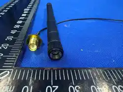
Explanation: The EUT has a Dipole antenna, and the antenna utilizes an RA-SMA connector, making it
difficult to replace.
Brand
Model Name
Antenna Type
Connector
Gain (dBi)
Note
TRULY
A25458101
Dipole
RA-SMA
2.4G:2.5
5G:2.50
2400-2500MHz
5150-5900MHz

2.8 Label and compliance information
Grantees are responsible for the continued compliance of their modules to the FCC/IC rules. This
includes advising host product manufacturers that they need to provide a physical or e-label stating
“Contains FCC ID” with their finished product. See Guidelines for Labeling and User Information for RF
Devices – KDB Publication 784748.
Explanation: The host system using this module, should have label in a visible area indicated the
following texts: “Contains Transmitter Module FCC ID: 2BOHY-621U1 Or Contains FCC ID: 2BOHY-
621U1”.
2.9 Information on test modes and additional testing requirements5
Additional guidance for testing host products is given in KDB Publication 996369 D04 Module Integration
Guide. Test modes should take into consideration different operational conditions for a stand-alone
modular transmitter in a host, as well as for multiple simultaneously transmitting modules or other
transmitters in a host product.
The grantee should provide information on how to configure test modes for host product evaluation for
different operational conditions for a stand-alone modular transmitter in a host, versus with multiple,
simultaneously transmitting modules or other transmitters in a host.
Grantees can increase the utility of their modular transmitters by providing special means, modes, or
instructions that simulates or characterizes a connection by enabling a transmitter. This can greatly
simplify a host manufacturer’s determination that a module as installed in a host complies with FCC/IC
requirements.
Explanation: Top band can increase the utility of our modular transmitters by providing instructions that
simulates or characterizes a connection by enabling a transmitter.
2.10 Additional testing, Part 15 Subpart B/ICES-003 disclaimer
The grantee should include a statement that the modular transmitter is only FCC authorized for the
specific rule parts (i.e., FCC/IC transmitter rules) listed on the grant, and that the host product
manufacturer is responsible for compliance to any other FCC/IC rules that apply to the host not covered
by the modular transmitter grant of certification. If the grantee markets their product as being Part 15
Subpart B/ICES-003 compliant (when it also contains unintentional-radiator digital circuity), then the
grantee shall provide a notice stating that the final host product still requires Part 15 Subpart B/ICES-003
compliance testing with the modular transmitter installed.
Explanation: The module without unintentional-radiator digital circuity, so the module does not require
an evaluation by FCC Part 15 Subpart B. The host shoule be evaluated by the FCC Subpart B.