
1
AC6956C Datasheet
Version:1.1
Date:2026.05.11

AC6956C Datasheet
2
AC6956C Features
CPU
32-bit DSP supports hardware Float Point
Unit(FPU)
Up to 240MHz programmable processor
64Vectored interrupts
4 Levels interrupt priority
DSP Audio Processing
SBC, AAC Audio decodes supported for BT
audio
mSBC voice codecs supported for BT phone
Supports MP2, MP3, WMA, APE, FLAC,
AAC, MP4, M4A, WAV, AIF, AIFC audio
decoding
Packet Loss Concealment (PLC) for voice
processing
Acoustic echo cancellation/suppression
(AEC,AES)
Single/Dual MIC Environmental Noise
Cancellation (ENC)
Multi-band DRC limiter
30-band EQ configuration for voice Effects
Audio Codec
Two channels 16-bit DAC, SNR >= 95dB
Three channels 16-bit ADC , SNR >= 90dB
Sampling rates of
8KHz/11.025KHz/16KHz/22.05KHz/24KHz/
32KHz/44.1KHz/48KHz are supported
One analog MIC amplifier, build-in MIC bias
generator
Supports two PDM digital MIC inputs
three channels Stereo analog MUX
Supports cap-less, single-ended, and
differential mode at the DAC path
Supports 16ohm and 32ohm Speaker loading
Bluetooth
Compliant with Bluetooth
V5.1+BR+EDR+BLE specification
Meet class1 class2 and class3 transmitting
power requirement
Provides +6dbm transmitting power
receiver with -90dBm sensitivity
Fast AGC for enhanced dynamic range
Supports
a2dp\avctp\avdtp\avrcp\hfp\spp\smp\att\gap\g
att\rfcomm\sdp\l2cap profile
Peripherals
One full speed USB 2.0 OTG controller
Four multi-function 16-bit timers, support
capture and PWM mode
Three 16-bit PWM generator for motor
driving
Three full-duplex basic UART, UART0 and
UART1 supports DMA mode
Two SPI interface supports host and device
mode
One hardware IIC interface supports host and
device mode
Built-in Cap Sense Key controller
10-bit ADC for analog sampling
External wake up/interrupt on all GPIOs
PMU
Low voltage LDO for internal digital and
analog circuit supply
3uA current consumption in the soft-off mode
Built-in LDO for the core, I/O, Bluetooth and
flash
VBAT is 2.2V to 5.5V
VDDIO is 2.2V to 3.6V
Packages
QFN32(4mm*4mm)

AC6956C Datasheet
2
Temperature
Operating temperature: -20℃ to +70℃
Storage temperature: -65℃ to +150℃
Applications
Bluetooth Stereo Sound Box
Bluetooth Mono Sound Box
Bluetooth TWS Sound Box
AC6956C Datasheet
2
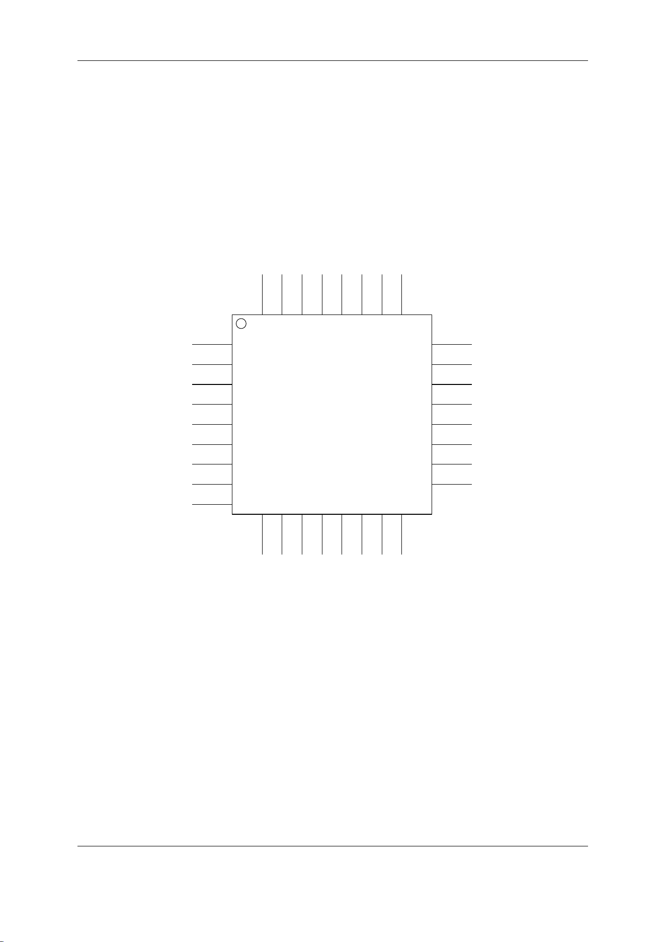
1、Pin Definition
1.1 Pin Assignment
1
2
3
4
5
6
7
8
9 10111213141516
17
18
19
20
21
22
23
24
32 31 30 29 28 27 26 25
PB8
BT_AVDD
VBAT
DACL
USBDM
PA0
PB0
PB3
PB2
VDDIO
DACVSS
MIC
AC6956C
(QFN32)
GND
BOM
VCOM USBDP
DACR
PC3
PC5
PC4
BT_OSCI
PB1
LDO_IN/PB5
FMIP
BT_OSC0
PA10
PA9
PA1
BT_RF
PB9
PB11
PB10
PC7
PC2
Figure 1-1 AC6956C Package Diagram
AC6956C Datasheet
3
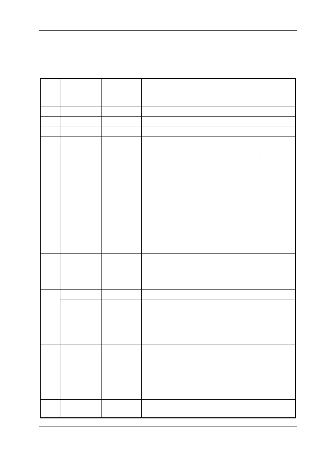
1.2 Pin Description
Table 1-1 AC6956C Pin Description
PIN
NO.
Name
I/O
Type
Drive
(mA)
Function Other Function
1 VCOM P / DAC Reference
2 DACL O / DAC Left Channel
3 DACR O / DAC Right Channel
4 FMIP I / FM Single Input
5 PB11 I/O / GPIO
SDPG:SDC Power Gate;
SPDIF_OUT:Sony/Philips Digital Interface Out
6 PB10 I/O 8/24 GPIO
AMUX2R:Analog Channel2 Right;
SPI2DOA:SPI2 Data Out(A);
ADC9:ADC Input Channel 9;
UART2RXC:Uart2 Data In(C);
PWMCH3L:Motor PWM Channel3(L);
7 PB9 I/O 8/24 GPIO
AMUX2L:Analog Channel2 Left;
SPI2CLKA:SPI2 Clk(A);
CAP0:Timer0 Capture;
UART2TXC:Uart2 Data Out(C);
PWMCH3H:Motor PWM Channel3(H);
8 PB8 I/O 8/24 GPIO
AMUX1R:Analog Channel1 Right;
SPI2_DIA:SPI2 Data In(A);
ADC8:ADC Input Channel 8;
CLKOUT1:Clk Out1;
9
LDO_IN P / Battery Charge Input
PB5 I/O 8
GPIO
(High Voltage
Resistance)
PWM3:Timer3 PWM Output;
CAP1:Timer1 Capture;
UART0TXC:Uart0 Data Out(C);
UART0RXC:Uart0 Data In(C);
10 VBAT P / Power Supply
11 BT_AVDD P / BT Power
12 PB3 I/O 8/24 GPIO
PWM2:Timer2 PWM Output;
ADC6:ADC Input Channel 6;
13 PB2 I/O 8
GPIO
(High Voltage
Resistance)
SPI1DIA:SPI1 Data In(A);
PWMCH1L:Motor PWM Channel1 (L);
14 PB1 I/O 8/24
GPIO
(pull up)
Long Press Reset;
SPI1DOA:SPI1 Data Out(A);
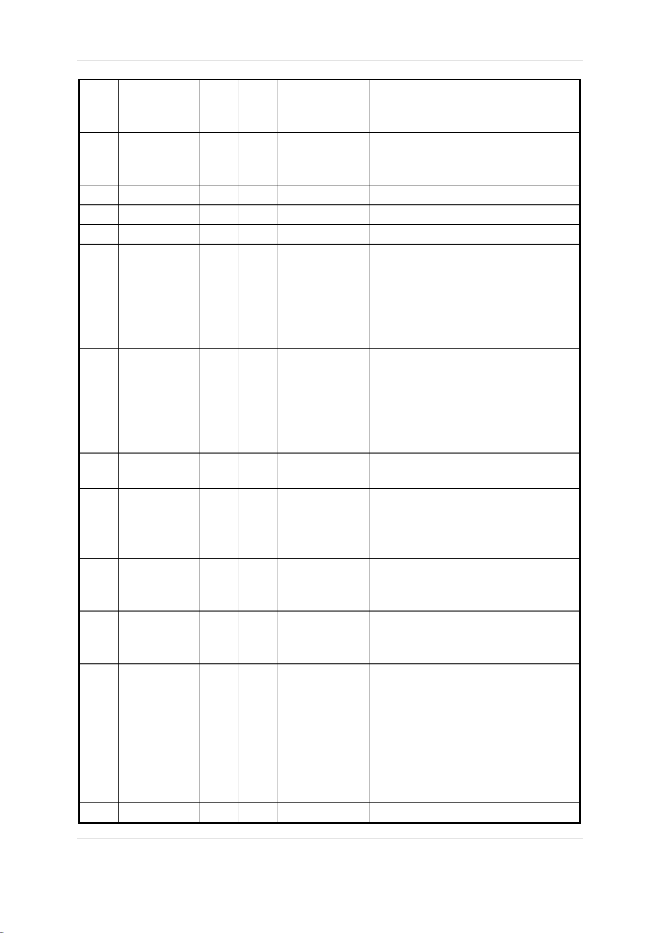
AC6956C Datasheet
4
ADC5:ADC Input Channel 5;
TMR2:Timer2 Clock Input;
UART1RXA:Uart1 Data In(A);
15 PB0 I/O 8
GPIO
(High Voltage
Resistance)
SPI1CLKA:SPI1 Clock(A);
UART1TXA:Uart1 Data Out(A);
PWMCH1H:Motor PWM Channel1(H);
16 BT_RF / / BT Antenna
17 BT_OSCI I / OSC In
18 BT_OSCO O / OSC Out
19 PC5 I/O 8/24 GPIO
SD1CLKA:SD1 Clock(A);
SPI1DOB:SPI1 Data Out(B);
UART2RXD:Uart2 Data In(D);
IIC_SDA_B:IIC SDA(B);
ADC13:ADC Input Channel 13;
PWMCH5L:Motor PWM Channel5(L);
20 PC4 I/O 8/24 GPIO
SD1CMDA:SD1 Command(A);
SPI1CLKB:SPI1 Clock(B);
UART2TXD:Uart2 Data Out(D);
IIC_SCL_B:IIC SCL(B); ADC10:ADC Input
Channel 10;
PWMCH5H:Motor PWM Channel5(H);
21 PC3 I/O 8/24 GPIO
SD1DAT0A:SD1 Data0(A);
SPI1DIB:SPI1 Data In(B);
22 PC2 I/O 8/24 GPIO
SD1DAT1A:SD1 Data1(A); ALNK1_DAT0:
Audio Link Data0;
Touch12:Touch Input Channel 12;
FPIN5:Motor Auto-Stop Protective Pin5;
23 USBDM I/O 4
USB Negative
Data
(pull down)
UART1RXD:Uart1 Data In(D);
IIC_SDA_A:IIC SDA(A);
24 USBDP I/O 4
USB Positive Data
(pull down)
UART1TXD:Uart1 Data Out(D);
IIC_SCL_A:IIC SCL(A);
ADC12:ADC Input Channel 12;
25 PA10 I/O 8/24 GPIO
SD0CLKA:SD0 Clock(A);
ALNK0_LRCKB:Audio Link Word Select(B);
ADC3:ADC Input Channel 3; SPDIF_IN_B:
Sony/Philips Digital Interface Input(B)
TMR1:Timer1 Clock Input;
Touch9:Touch Input Channel 9;
UART2RXB:Uart2 Data In(B);
PWMCH4L:Motor PWM Channel4(L);
26 PA9 I/O 8/24 GPIO
SD0CMA:SD0 Command(A);
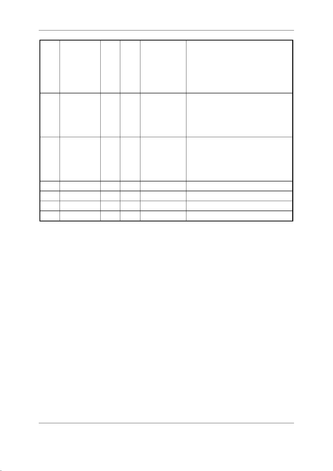
AC6956C Datasheet
5
ALNK0_SCLKB:Audio Link Serial Clock(B);
SPDIF_IN_A:Sony/Philips Digital Interface
Input(A)
Touch8:Touch Input Channel 8;
UART2TXB:Uart2 Data Out(B);
PWMCH4H:Motor PWM Channel4(H);
27 PA1 I/O 8/24 GPIO
AMUX0R:Analog Channel0 Right;
Touch1:Touch Input Channel 1;
ADC0:ADC Input Channel 0;
UART1RXC:Uart1 Data In(C);
PWMCH0L:Motor PWM Channel0(L);
28 PA0 I/O 8/24 GPIO
AMUX0L:Analog Channel0 Left;
Touch0:Touch Input Channel 0;
CLKOUT0:
UART1TXC:Uart1 Data Out(C);
PWMCH0H:Motor PWM Channel0(H);
29 PC7 I/O / GPIO
MIC_BIAS:Microphone Bias Output
30 MIC I /
MIC:MIC Input Channel;
31 VDDIO P / IO Power 3.3v
32 DACVSS P / DAC Ground
AC6956C Datasheet
6
2、Electrical Characteristics
2.1 Absolute Maximum Ratings
Table 2-1
Symbol Parameter Min Max Unit
Tamb Ambient Temperature -20 +70 °C
Tstg Storage temperature -65 +150 °C
VBAT Supply Voltage 2.2 5.5 V
LDO_IN Charger Voltage 4.5 5.5 V
V
3.3IO
3.3V IO Input Voltage -0.3 VDDIO+0.3 V
2.2 PMU Characteristics
Table 2-2
Symbol Parameter Min Typ Max Unit Test Conditions
VBAT Voltage Input 2.2 3.7 5.5 V
LDO_IN Charger Voltage 4.5 5.0 5.5 V
V
3.3
Voltage output _ 3.3 _ V VBAT = 5V, 100mA loading
V
BT_AVDD
Voltage output 1.3 V VBAT=5V, 100mA loading
V
DACVDD
DAC Voltage _ 2.7 _ V VBAT = 5V, 10mA loading
I
L3.3
Loading current _ _ 150 mA VBAT = 5V
2.3 Battery Charge
Table 2-3
Symbol Parameter Min Typ Max Unit Test Conditions
LDO_IN
Charge Input
Voltage
4.5 5 5.5 V _
V
Charge
Charge Voltage 4.15 4.2 4.25 V _
I
Charge
Charge Current 20 320 mA Charge current at fast charge mode
I
Trikl
Trickle Charge
Current
20 45 70 mA V
BAT
<V
Trikl
AC6956C Datasheet
7
2.4 IO Input/Output Electrical Logical Characteristics
Table 2-4
IO input characteristics
Symbol Parameter Min Typ Max Unit Test Conditions
V
IL
Low-Level Input
Voltage
-0.3 _ 0.3* VDDIO V VDDIO = 3.3V
V
IH
High-Level Input
Voltage
0.7*
VDDIO
_ VDDIO+0.3 V VDDIO = 3.3V
IO output characteristics
V
OL
Low-Level Output
Voltage
_ _ 0.33 V VDDIO = 3.3V
V
OH
High-Level Output
Voltage
2.7 _ _ V VDDIO = 3.3V
2.5 Internal Resistor Characteristics
Table 2-5
Port
General
Output
High Drive
Internal
Pull-Up
Resistor
Internal
Pull-Down
Resistor
Comment
PA0、PA1
PA9、PA10
PB1、PB3
PB8~PB10
PC2~PC5
8mA 24mA 10K 10K
1、PB1 default pull up
2、USBDM & USBDP
default pull down
3、PB0, PB2, PB5 can
pull-up resistance to
5V
4、internal
pull-up/pull-down
resistance | accuracy
±20%
5、PRx supply by
RTCVDD
PB11
PC7
Output 0 8mA 24mA
10K 10K
Output 1 8mA 64mA
PB0、PB2
PB5
8mA _ 10K 10K
USBDP 4mA _ 1.5K 15K
USBDM
4mA
_
180K 15K
AC6956C Datasheet
8
2.6 DAC Characteristics
Table 2-6
Parameter Min Typ Max Unit Test Conditions
Frequency Response 20 _ 20K Hz
1KHz/0dB
10Kohm loading
With A-Weighted Filter
THD+N _ -75 _ dB
S/N _ 95 _ dB
Crosstalk _ -90 _ dB
Output Swing 1 Vrms
Dynamic Range
90 dB
1KHz/-60dB
10Kohm loading
With A-Weighted Filter
DAC Output Power 11 _ mW 32ohm loading
2.7 ADC Characteristics
Table 2-7
Parameter Min Typ Max Unit Test Conditions
Dynamic Range 80 dB 1KHz/-60dB
S/N _ 90 91 dB
1KHz/-60dB THD+N _ -70 _ dB
Crosstalk _ -80 _ dB
2.8 BT Characteristics
2.8.1 Transmitter
Basic Data Rate Table 2-8
Parameter Min Typ Max Unit Test Conditions
RF Transmit Power
25℃,
Power Supply
VBAT=5V
2441MHz
RF Power Control Range 20 dB
20dB Bandwidth 950 KHz
Adjacent Channel
Transmit Power
+2MHz -40 dBm
-2MHz -38 dBm
+3MHz -44 dBm
-3MHz -35 dBm
0.52
dBm
AC6956C Datasheet
9
Enhanced Data Rate Table 2-9
Parameter Min Typ Max Unit Test Conditions
Relative Power -1 dB
25℃,
Power Supply
VBAT=5V
2441MHz
Adjacent Channel
Transmit Power
+2MHz -40 dBm
-2MHz -38 dBm
+3MHz -44 dBm
-3MHz -35 dBm
2.8.2 Receiver
Basic Data Rate
Table 2-10
Parameter Min Typ Max Unit Test Conditions
Sensitivity -90 dBm
25℃,
Power Supply
VBAT=5V
2441MHz
Co-channel Interference Rejection -13 dB
Adjacent Channel
Interference Rejection
+1MHz +5 dB
-1MHz +2 dB
+2MHz +37 dB
-2MHz +36 dB
+3MHz +40 dB
-3MHz +35 dB
Enhanced Data Rate Table 2-11
Parameter Min Typ Max Unit Test Conditions
Sensitivity -90 dBm
25℃,
Power Supply
VBAT=5V
2441MHz
Co-channel Interference Rejection -13 dB
Adjacent Channel
Interference Rejection
+1MHz +5 dB
-1MHz +2 dB
+2MHz +37 dB
-2MHz +36 dB
+3MHz +40 dB
-3MHz +35 dB
AC6956C Datasheet
10
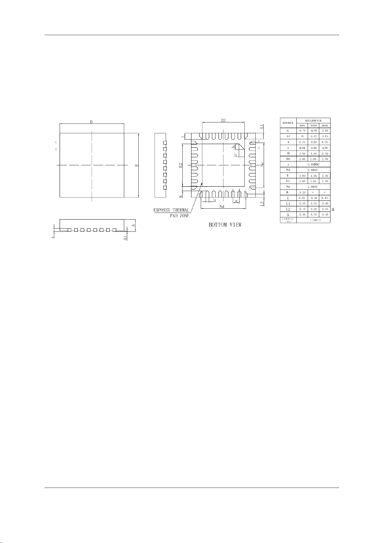
3、 Package Information
3.1 QFN32_4x4
Figure 3-1 AC6956C Package

AC6956C Datasheet
11
4.Summarize the specific operational use conditions
4.1. This modular transmitter is only for professional technicians to install, debug, and
maintain. Non-professionals are not allowed to replace the antenna, configure power
parameters, or modify the RF link without authorization.
4.2. All usage restrictions, antenna constraints, power limits, and installation
specifications of this module also apply to the accompanying user manual provided by the
main unit manufacturer. The main unit manufacturer must fully quote and incorporate all
the constraints of this module into the product manual of the main unit, and publicize the
compliance requirements for end users.
5. Human Safety Distance Requirements: This product is a mobile device type. To meet
radio frequency radiation safety standards, the distance between the product and the
human body must be greater than 5mm during normal operation. This distance
requirement must be strictly adhered to during use and installation. It is not allowed to use
the product in scenarios where the distance to the human body is less than 5mm. The
overall design of the host device must meet this safety distance specification to ensure
that terminal usage complies with relevant radiation safety regulations.
6. Antenna Type
Plannar Inverted F Antenna on board
7. Module have received FCC “Modular Approvals”, in compliance with CFR 47 FCC part 15
Subpart C regulations
This device complies with Part 15 of the FCC Rules. Operation is subject to the following two conditions:
(1) This device may not cause harmful interference, and (2) this device must accept any interference
received, including interference that may cause undesired operation.
FCC Caution: Any changes or modifications not expressly approved by the party responsible for
compliance could void the user's authority to operate this equipment.
WARNING!
FCC Radiation Exposure Statement:
This portable equipment with its antenna complies with FCC’s RF radiation exposure limits set forth for
an uncontrolled environment. To maintain compliance follow the instructions below;
1. This transmitter must not be co-located or operating in conjunction with any other antenna or
transmitter.
2. Avoid direct contact to the antenna, or keep it to a minimum while using this equipment.
This transmitter module is authorized to be used in other devices only by OEM integrators under
the following condition:
The transmitter module must not be co-located with any other antenna or transmitter.
As long as the above condition is met, further transmitter testing will not be required. However, the OEM
integrator is still responsible for testing their end-product for any additional compliance requirements
required with this module installed (for example, digital device emissions, PC peripheral requirements,
etc.).
8. The OEM must ensure that FCC labeling requirements are met. This shall include a
clearly visible label on the exterior of the end product with the following nomenclature:
Contains FCC ID: 2BR5R58000
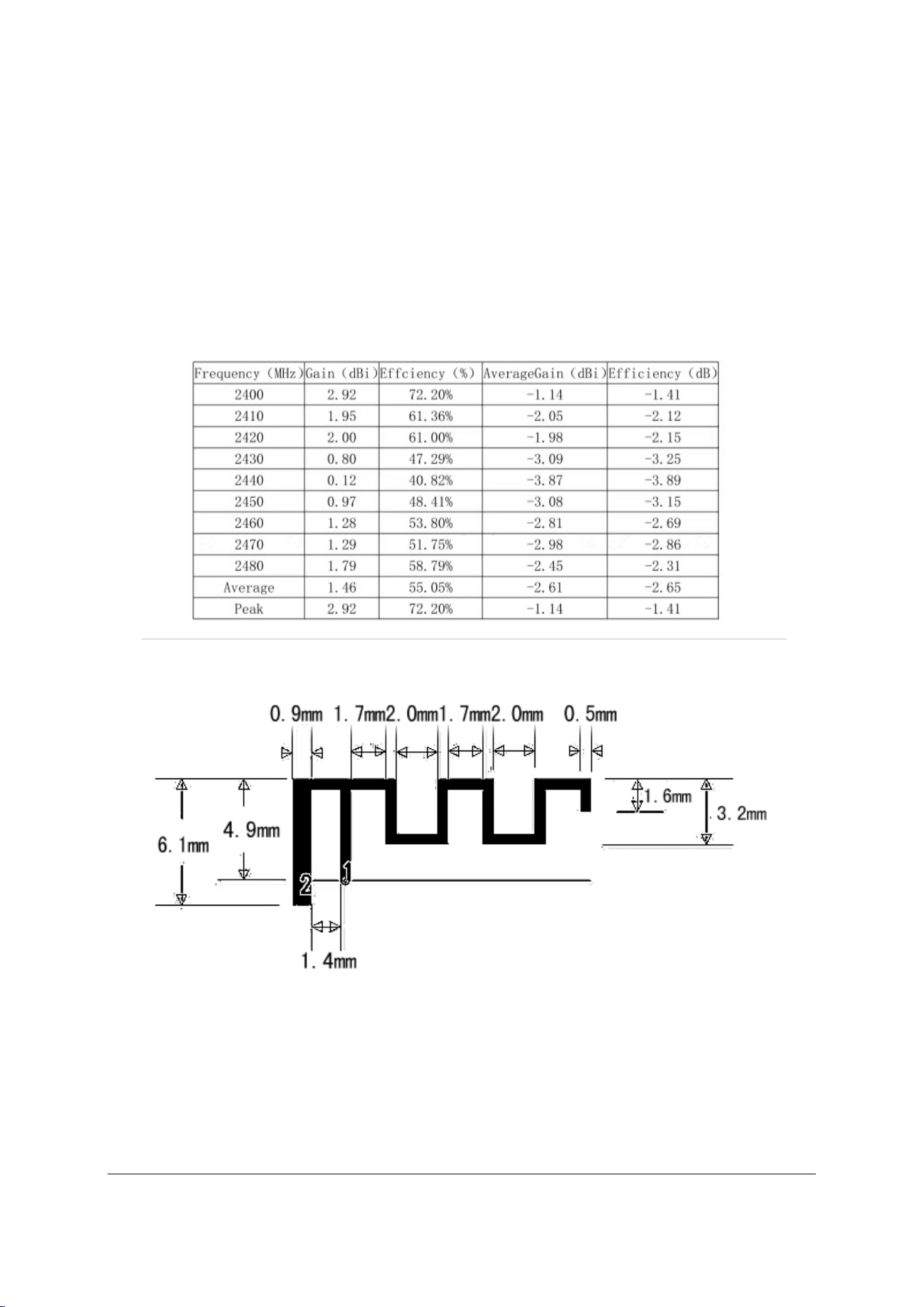
9. Antenna efficiency and gainn
10.Trace antenna designs
11.The host product manufacturer is responsible for compliance to any other FCC rules
that apply to the host not covered by the modular transmitter grant of certifcation.The final
host product still requires Part 15 Subpart B compliance testing with the modular
transmitter installed.
12

13
12 、Revision History
Date Revision Description
2026.05.11 V1.0 Initial Release