

Contents
© 2026 Beken Corporation 2 DS-BKSG2-MINI-E03 V1.2
Contents
Contents ............................................................................................................................................................................. 2
1. Module Overview ....................................................................................................................................................... 4
2. Module Outline ........................................................................................................................................................... 5
2.1
2.2
2.3 Module Laser Marking .................................................................................................................................................................
Module Dimensions......................................................................................................................................................................5
Module Outline With Designators...............................................................................................................................................6
6
2.4 Module PCB Solder Mask ........................................................................................................................................................... 6
2.5 Module PCB Antenna .................................................................................................................................................................. 7
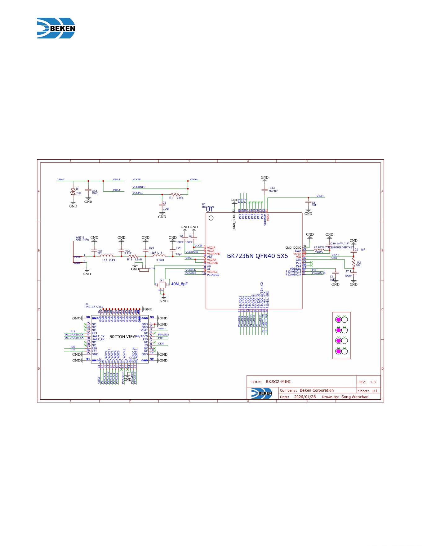
2.6 Schematic ...................................................................................................................................................................................... 7
4.1
3. Pin Descriptions.........................................................................................................................................................8
4. Electrical Characteristics..........................................................................................................................................11
4.2
4.3
4.4 Current Consumption .................................................................................................................................................................
Recommended Operating Conditions.....................................................................................................................................11
Digital I/O Characteristics...........................................................................................................................................................
Absolute Maximum Ratings......................................................................................................................................................11
11
12
4.5
4.6
4.7
4.8
4.9 WLAN RF Transmitter Characteristics .....................................................................................................................................
ESD Ratings................................................................................................................................................................................14
WLAN RF Receiver Characteristics.........................................................................................................................................
CENTiming.................................................................................................................................................................................13
Moisture Sensitivity Level...........................................................................................................................................................14
14
16
4.10 Bluetooth LE RF Receiver Characteristics .............................................................................................................................. 17
4.11 Bluetooth LE RF Transmitter Characteristics .......................................................................................................................... 19
4.12 AUX ADC Characteristics .......................................................................................................................................................... 21
4.13 I2C Characteristics ..................................................................................................................................................................... 21
4.14 PWM Characteristics .................................................................................................................................................................. 22
4.15 NTC Characteristics ................................................................................................................................................................... 22

Contents
© 2026 Beken Corporation 3 DS-BKSG2-MINI-E03 V1.2
5. Module Burning and Test Mode ............................................................................................................................. 23
5.1 Firmware Download ................................................................................................................................................................... 23
5.2 Enter Test Mode .......................................................................................................................................................................... 24
6. Packge information and ordering number ............................................................................................................. 25
6.1 Packge information ..................................................................................................................................................................... 25
6.2 Ordering number ........................................................................................................................................................................ 26
7. Certification .............................................................................................................................................................. 27
7.1 Revision History .......................................................................................................................................................................... 28

Module Overview
© 2026 Beken Corporation 4 DS-BKSG2-MINI-E03 V1.2
1. Module Overview
The BKSG2-MINI is a low-power, high-performance Wi-Fi + Bluetooth LE module. It consists of the BK7236N SoC and
peripheral resistors and capacitors, crystal oscillators, buck inductors, and onboard PCB antenna. It is a 1x1 single-band 2.4
GHz Wi-Fi 6 and Bluetooth 5.2 combo solution. The module also has a simple and easy-to-use interface targeted for lighting
4 MB flash and 512
applications. A variety of products can be developed based on this module.
The BK7236N integrates a 32-bit Armv8-M STAR-MC1 MCU that operates at 160 MHz by default. It also incorporates
KB RAM.
Module Outline
© 2026 Beken Corporation 5 DS-BKSG2-MINI-E03 V1.2
2. Module Outline
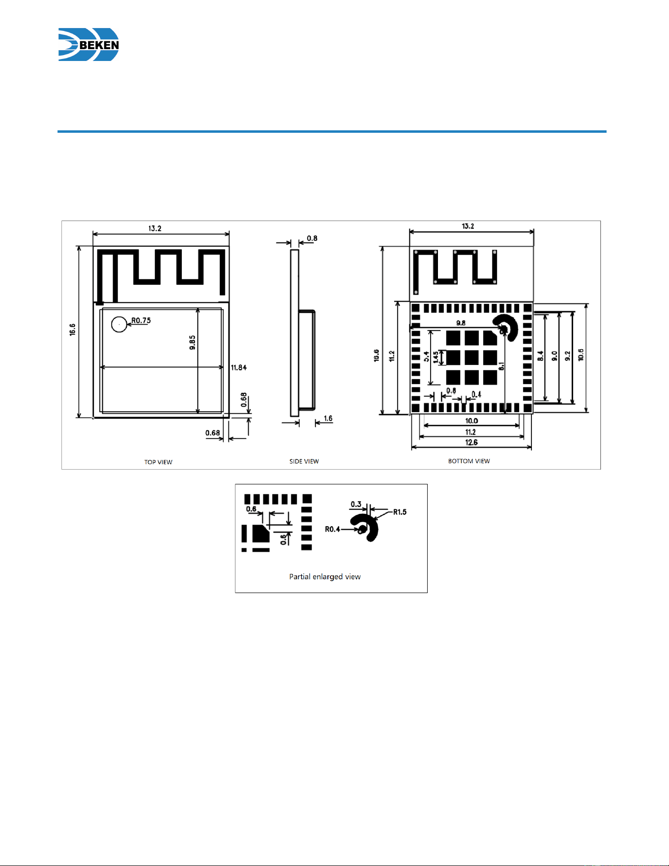
2.1 Module Dimensions
Figure 2-1 Module Dimensions (Unit:mm)
The module dimensions are as below:
• Length: 16.6 mm
• Width: 13.2 mm
• Board thickness: 0.8 mm
• Maximum overall thickness: 3.2 mm
Module Outline
© 2026 Beken Corporation 6 DS-BKSG2-MINI-E03 V1.2
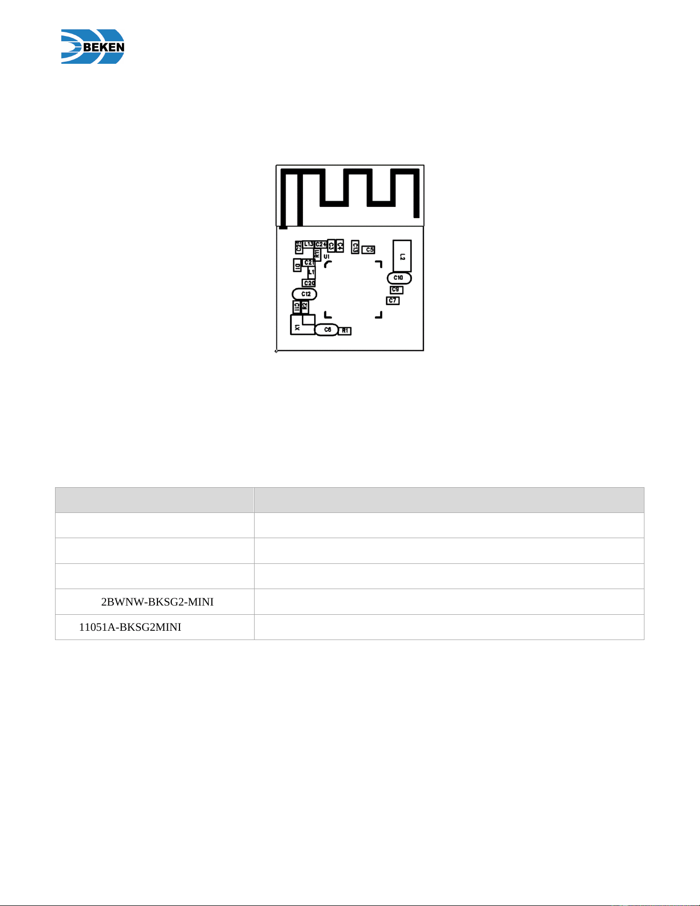
2.2 Module Outline With Designators
Figure 2-2 Module Outline with Designators (Top View)
2.3 Module Laser Marking
The laser marking on the module shielding cover includes a QR code and also the following information shown in Table 2-1.
Table 2-1 Module Laser Marking
Marking
Description
BEKEN
Brand name
CE
CE marking
BKSG2-MINI
Model name
FCC ID:2BWNW-BKSG2-MINI
FCC ID
IC
IC:
11051A-BKSG2MINI
ID
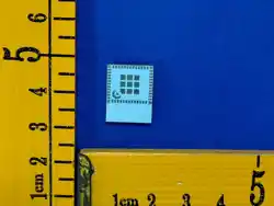
The picture of module:
2.4 Module PCB Solder Mask
The color of the module PCB solder mask should be white.
Pin Descriptions
© 2026 Beken Corporation 8 DS-BKSG2-MINI-E03 V1.2
3. Pin Descriptions
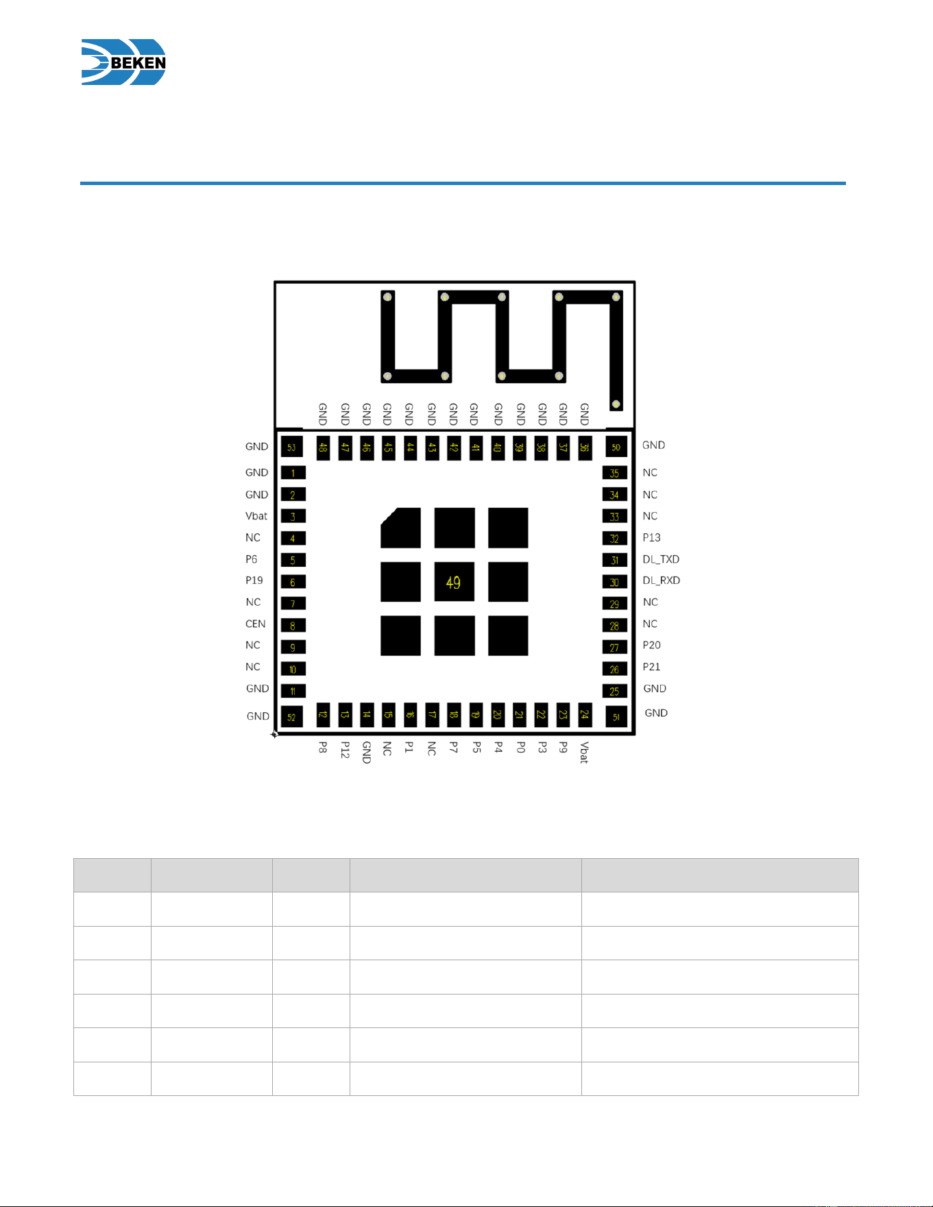
Figure 3-1 shows the pin assignments of the module.
Figure 3-1 Pin Assignments (Bottom Layer, Top View)
Table 3-1 Pin Descriptio
Table 3-1 shows the pin descriptions of the module.
ns
Pin #
Name
Type
Default State After Power-on
Description
1
GND
P
-
Ground
2
GND
P
-
Ground
3
VBAT
P
-
Chip external power supply input
4
NC
- -
No connect
5
P6
IO
Digital/Analog
GPIO6, ADC5
6
P19
IO
Digital
GPIO19,PWM1

Pin Descriptions
© 2026 Beken Corporation 9 DS-BKSG2-MINI-E03 V1.2
Pin #
Name
Type
Default State After Power-on
Description
7
NC
- -
No connect
8
CEN
I 10 kΩ pulled up to VIO
Chip enable, active high
9
NC
- -
No connect
10
NC
- -
No connect
11
GND
P -
Ground
12
P8
IO Digital/Analog
GPIO8, ADC10
13
P12
IO Digital/Analog
GPIO12, ADC14
14
GND
P -
Ground
15
NC
- -
No connect
16
P1
IO Digital/Analog
GPIO1, UART1_RX, I2C1_SDA
17
NC
- -
No connect
18
P7
IO Digital/Analog
GPIO7, PWM4/ADC6
19
P5
IO
Digital/Analog
GPIO5, PWM0/ADC4
20
P4
IO
Digital/Analog
GPIO4, PWM2/ADC3
21
P0
IO
Digital/Analog
GPIO0, I2C1_SCL/ADC12
22
P3
IO
Digital/Analog
GPIO3, ADC2
23
P9
IO
Digital/Analog
GPIO9
24
VBAT
P
-
Power supply output for I2C led driver
chip
25
NC
-
-
No connect
26
P21
IO
Digital
GPIO21, UART2_RX
27
P20
IO
Digital
GPIO20, UART2_TX
28
NC
-
-
No connect
29
NC
-
-
No connect
30
DL_RXD
IO
Digital
GPIO10, DL_UART_RX, UART0_RX
31
DL_TXD
IO
Digital
GPIO11, DL_UART_TX, UART0_TX
32
P13
IO Digital/Analog
GPIO13, PWM3,ADC15
33
NC
-
-
No connect
Pin Descriptions
© 2026 Beken Corporation 10 DS-BKSG2-MINI-E03 V1.2
Pin #
Name
Type
Default State After Power-on
Description
34
NC
- -
No connect
35
NC
- -
No connect
36–48
GND
P -
Ground
49
PAD
P -
Ground pad, connected to GND
50–53
GND
- -
Ground

Electrical Characteristics
© 2026 Beken Corporation 11 DS-BKSG2-MINI-E03 V1.2
4. Electrical Characteristics
4.1 Absolute Maximum Ratings
Parameter
Description
Min.
Max.
Unit
VBAT
Power supply input
-0.3
4.5
V
I
max
VBAT maximum current
-
400
mA
V
DIG_A
Voltage on any digital pin
-0.3
VIO+0.3
V
T
STR
Storage temperature range
-55
150
°C
4.2 Recommended Operating Conditions
Parameter
Description
Min.
Typ.
Max.
Unit
T
OPR
Operating temperature range (shielding cover
temperature)
-40
-
105
°C
VBAT
Power supply input
2.4
3.3
3.6
V
VIO
I/O voltage
2.4
3.3
3.6
V
Vpp
Ripple on the VBAT
-
-
200
mV
4.3 Digital I/O Characteristics
Symbol
Parameter
Conditions
Min.
Typ.
Max.
Unit
VIH
High-level input voltage
-
0.7 VIO
-
VIO + 0.3
V
VIL
Low-level input voltage
-
-0.3
-
0.3 VIO
V
VOH
High-level output voltage
-
0.9 VIO
-
-
V
VOL
Low-level output voltage
-
-
-
0.1 VIO
V
I
OH
I/O output high drive
strength
VOH: 0.8 VIO,
GPIO_CAPACITY =
3
40
mA
VOH: 0.8 VIO,
GPIO_CAPACITY =
30

Electrical Characteristics
© 2026 Beken Corporation 12 DS-BKSG2-MINI-E03 V1.2
Symbol
Parameter
Conditions
Min.
Typ.
Max.
Unit
2
VOH = 0.8 VIO,
GPIO_CAPACITY =
1
18
VOH = 0.8 VIO,
GPIO_CAPACITY =
0
10
I
OL
I/O output low drive strength
VOH: 0.15 VIO,
GPIO_CAPACITY =
3
36
mA
VOH: 0.15 VIO,
GPIO_CAPACITY =
2
29
VOH = 0.15 VIO,
GPIO_CAPACITY =
1
16
VOH = 0.15 VIO,
GPIO_CAPACITY =
0
8
R
PU
Weak pull-up resistor
-
-
40
-
kΩ
R
PD
Weak pull-down resistor
-
-
44
-
kΩ
4.4 Current Consumption
Parameter
Condition
Min.
Typ.
Max.
Unit
Active Mode
RX current
11b, continuous receive, buck
-
-
-
mA
11b, continuous receive, LDO
-
37
-
mA
11b/g/n, 20 MHz, mixed mode, continuous
receive, buck
-
-
-
mA
11n40 MHz, mixed mode, continuous
receive, buck
-
-
-
mA
11b/g/n, 20 MHz, mixed mode, continuous
receive, LDO
-
42
-
mA
Electrical Characteristics
© 2026 Beken Corporation 13 DS-BKSG2-MINI-E03 V1.2
Parameter
Condition
Min.
Typ.
Max.
Unit
11n, 40 MHz, mixed mode, continuous
receive, LDO
-
46
-
mA
TX current
11b: 1 Mbps DSSS @ 20 dBm(LDO)
-
340
-
mA
11b: 1 Mbps DSSS @ 20 dBm(BUCK)
-
-
-
mA
11g: 54 Mbps OFDM @ 18 dBm(LDO)
-
310
-
mA
11g: 54 Mbps OFDM @ 18 dBm(BUCK)
-
mA
11n: MCS7, HT20 @ 17 dBm(LDO)
-
290
-
mA
11n: MCS7, HT20 @ 17 dBm(BUCK)
-
mA
Sleep Mode
Normal sleep
CPU active(60Mhz), Wi-Fi MAC on, Wi-Fi
PHY off, Bluetooth off, multimedia (audio,
video) off, encryption off
-
6
-
mA
Low-voltage sleep
CPU halted, Wi-Fi MAC halted, Wi-Fi PHY
off, Bluetooth off, encryption off, SMEM3 off,
XTALH off, VDDDIG=0.6 V
91
μA
Deep sleep
Only the AON domain is active.
-
13.7
-
μA
Shutdown Mode
Shutdown
CEN low
-
3.2
-
μA
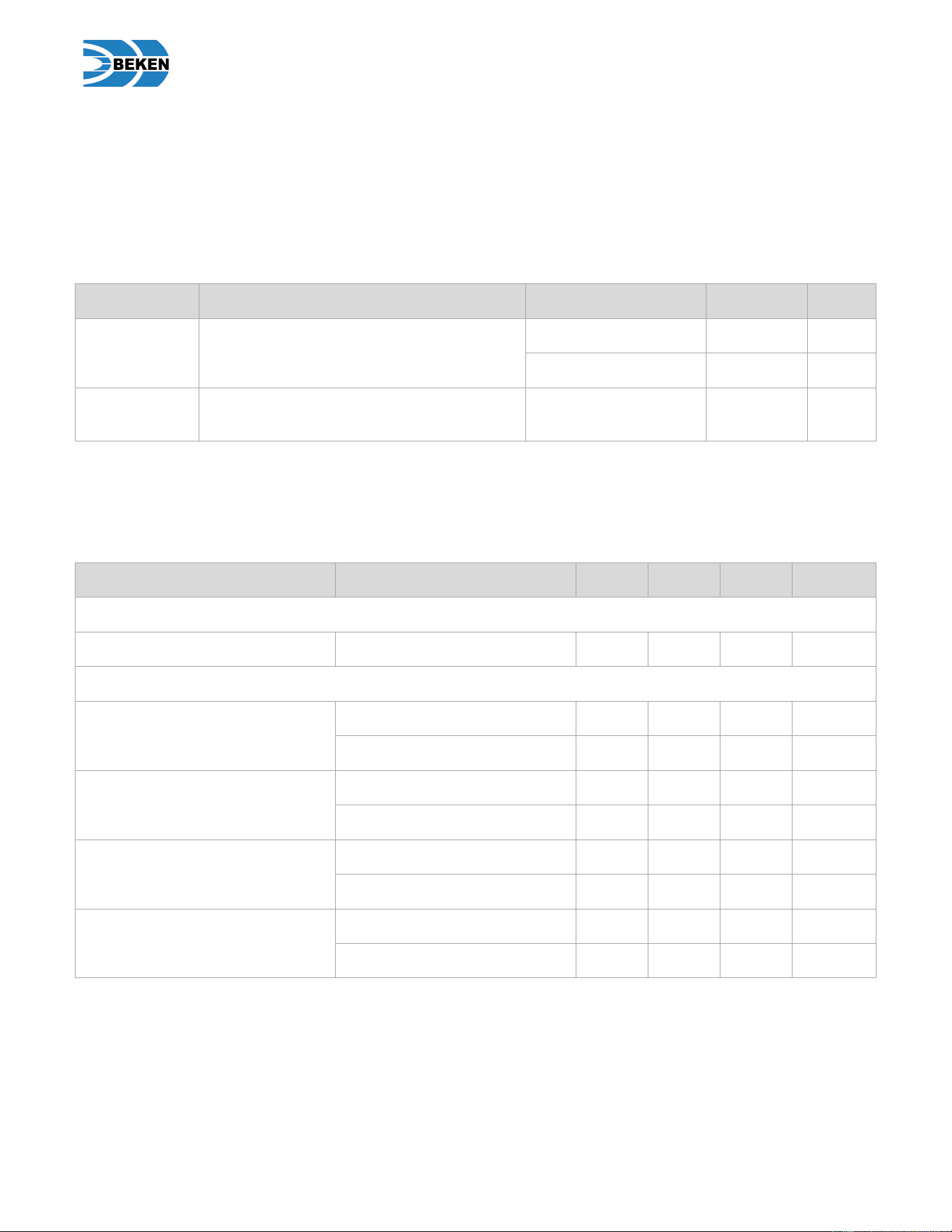
4.5 CEN Timing
Parameter
Description
Min.
Max.
Unit
T
CEN_Min
minimum pull-low time for CEN reset
1
-
ms
V
CEN_IL
CEN input low level
-
1
V
Figure 4-1 CEN Signal Waveform Requirements
Electrical Characteristics
© 2026 Beken Corporation 14 DS-BKSG2-MINI-E03 V1.2
4.6 Moisture Sensitivity Level
The Module is qualified to moisture sensitivity level MSL3 in accordance with IPC/JEDEC J-STD-020.
4.7 ESD Ratings
Parameter
Description
Test Condition
Value
Unit
ESD HBM
Electrostatic discharge voltage (human body
model), per ANSI/ESDA/JEDEC JS-001
ANT pin
±2000
V
Other pins
±3000
V
ESD CDM
Electrostatic discharge voltage (charge device
model), per ANSI/ESDA/JEDEC JS-002
All pins
±500
V
4.8 WLAN RF Receiver Characteristics
Measured with T = 25 °C , VBAT = 3.3 V unless otherwise stated.
Parameter
Condition
Min.
Typ.
Max.
Unit
General
Frequency range
-
2412
-
2484
MHz
Sensitivity
Sensitivity - IEEE 802.11b
(8% PER for PSDU)
1 Mbps DSSS
-
-98
-
dBm
11 Mbps DSSS
-
-89
-
dBm
Sensitivity - IEEE 802.11g
(10% PER for PSDU)
6 Mbps OFDM
-
-92
-
dBm
54 Mbps OFDM
-
-76.5
-
dBm
Sensitivity - IEEE 802.11n, 20 MHz
(10% PER for PSDU, BCC)
HT20, MCS0
-
-92
-
dBm
HT20, MCS7
-
-73
-
dBm
Sensitivity - IEEE 802.11n, 40 MHz
(10% PER for PSDU, BCC)
HT40, MCS0
-
-87.5
-
dBm
HT40, MCS7
-
-71.5
-
dBm

Electrical Characteristics
© 2026 Beken Corporation 15 DS-BKSG2-MINI-E03 V1.2
Parameter
Condition
Min.
Typ.
Max.
Unit
Maximum Receive Level
Maximum receive level @ 2.4 GHz
11b: 1, 2 Mbps (8% PER, 1024
octets)
-
10
-
dBm
11b: 5.5, 11 Mbps (8% PER, 1024
octets)
-
10
-
dBm
11g: 6–54 Mbps (10% PER, 1000
octets)
-
0
-
dBm
11n: MCS0–7 (10% PER, 4096
octets)
-
0
-
dBm
Adjacent Channel Rejection
Adjacent channel (±30 MHz) rejection
- IEEE 802.11b
(8% PER for 1024 octet PSDU with
desired signal level as specified in
Condition)
1 Mbps DSSS -74 dBm
-
50
-
dB
2 Mbps DSSS
-74 dBm
-
45
-
dB
Adjacent channel (±25 MHz) rejection
- IEEE 802.11b
(8% PER for 1024 octet PSDU with
desired signal level as specified in
Condition)
5.5 Mbps DSSS
-70 dBm
-
43
-
dB
11 Mbps DSSS
-70 dBm
-
40
-
dB
Adjacent channel (±25 MHz) rejection
- IEEE 802.11g
(10% PER for 1000 octet PSDU with
desired signal level as specified in
Condition)
6 Mbps OFDM
-79 dBm
-
43
-
dB
54 Mbps OFDM
-62 dBm
-
27
-
dB
Adjacent channel (±25 MHz) rejection
- IEEE 802.11n
(10% PER for 4096 octet PSDU with
desired signal level as specified in
Condition)
HT20, MCS0
-79 dBm
-
43
-
dB
HT20, MCS7
-61 dBm
-
21
-
dB
Spurious Emissions
Spurious emissions
< 1 GHz
-
-60
-
dBm
> 1 GHz
-
-50
-
dBm

Electrical Characteristics
© 2026 Beken Corporation 16 DS-BKSG2-MINI-E03 V1.2
4.9 WLAN RF Transmitter Characteristics
Measured with T = 25 °C , VBAT = 3.3 V unless otherwise stated.
Parameter
Condition
Min.
Typ.
Max.
Unit
General
Frequency range
-
2412
-
2484
MHz
TX Power
TX power - IEEE 802.11b
(SEM compliant)
1 Mbps DSSS
-
20
-
dBm
11 Mbps DSSS
-
20
-
dBm
TX power - IEEE 802.11g
(EVM compliant)
6 Mbps OFDM
-
18
-
dBm
54 Mbps OFDM
-
18
-
dBm
TX power - IEEE 802.11n
(EVM compliant)
HT20, MCS0
-
17
-
dBm
HT20, MCS7
-
17
-
dBm
HT40, MCS0
-
16
-
dBm
HT40, MCS7
-
16
-
dBm
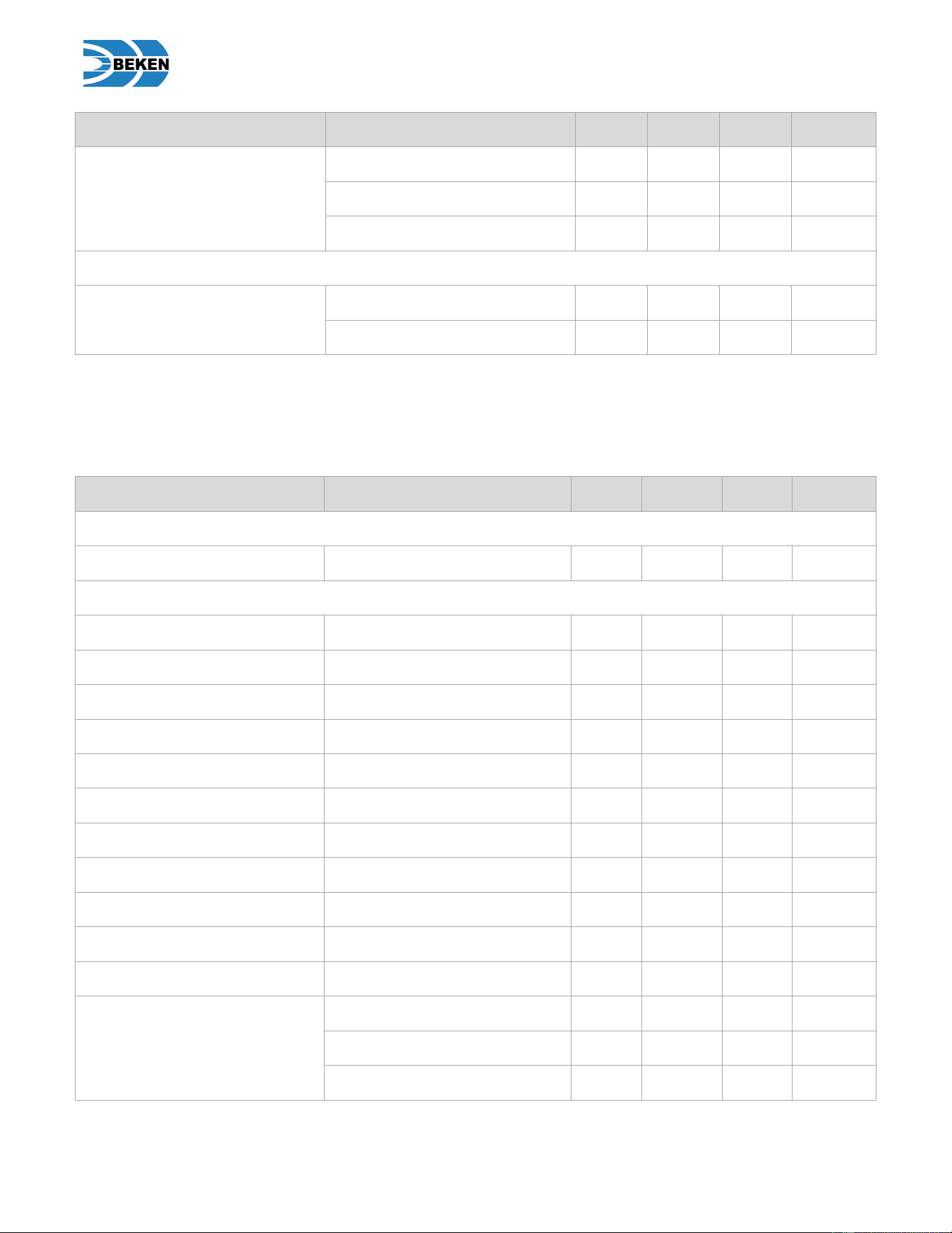
TX EVM
TX EVM - IEEE 802.11b
(SEM compliant)
1 Mbps DSSS, @20dBm - -15 - dB
11 Mbps DSSS, @20dBm - -15 - dB
TX EVM - IEEE 802.11g
6 Mbps OFDM, @18dBm - -27 - dB
54 Mbps OFDM, @18dBm - -27 - dB
TX EVM - IEEE 802.11n
HT20, MCS0, @17dBm - -29 - dB
HT20, MCS7, @17dBm - -29 - dB
HT40, MCS0, @16dBm - -29 - dB
HT40, MCS7, @16dBm - -29 - dB
Electrical Characteristics
© 2026 Beken Corporation 17 DS-BKSG2-MINI-E03 V1.2
Parameter
Condition
Min.
Typ.
Max.
Unit
HE20, MCS7, @17dBm
-
-30
-
dB
HE40, MCS0, @16dBm
-
-30
-
dB
HE40, MCS7, @16dBm
-
-30
-
dB
Spurious Emissions
Spurious emissions (at maximum
output power)
< 1 GHz
-
-50
-
dBm
> 1 GHz
-
-45
-
dBm
4.10 Bluetooth LE RF Receiver Characteristics
Measured with T = 25 °C , VBAT = 3.3 V unless otherwise stated.
Parameter
Condition
Min.
Typ.
Max.
Unit
General
Frequency range
-
2402
-
2480
MHz
Bluetooth LE 1 Mbps
Sensitivity
30.8% PER
-
-97
-
dBm
Maximum input level
30.8% PER
-
0
-
dBm
C/I co-channel
-
-
8
-
dB
C/I 1 MHz adjacent channel
-
-
0
-
dB
C/I -1 MHz adjacent channel
-
-
0
-
dB
C/I 2 MHz adjacent channel
-
-
-26
-
dB
C/I -2 MHz adjacent channel
-
-
-27
-
dB
C/I 3 MHz adjacent channel
-
-
-28
-
dB
C/I -3 MHz adjacent channel
-
-
-29
-
dB
C/I > 3 MHz adjacent channel
-
-
-50
-
dB
C/I < -3 MHz adjacent channel
-
-
-50
-
dB
Out-of-band blocking
30–2000 MHz
-10
-
-
dBm
2003–2399 MHz
-12
-
-
dBm
2484–2997 MHz
-12
-
-
dBm

Electrical Characteristics
© 2026 Beken Corporation 18 DS-BKSG2-MINI-E03 V1.2
Parameter
Condition
Min.
Typ.
Max.
Unit
3000 MHz–12.75 GHz
-2
-
-
dBm
Bluetooth LE 125 kbps
Sensitivity 30.8% PER - -102 - dBm
Maximum input level 30.8% PER - 0 - dBm
C/I co-channel - - 3
-
dB
C/I 1 MHz adjacent channel - - -15
-
dB
C/I -1 MHz adjacent channel - - -16
-
dB
C/I 2 MHz adjacent channel - - -34
-
dB
C/I -2 MHz adjacent channel - - -40
-
dB
C/I 3 MHz adjacent channel - - -42
-
dB
C/I -3 MHz adjacent channel - - -43
-
dB
C/I > 3 MHz adjacent channel - - -41
-
dB

Electrical Characteristics
© 2026 Beken Corporation 19 DS-BKSG2-MINI-E03 V1.2
Parameter
Condition
Min.
Typ.
Max.
Unit
C/I < -3 MHz adjacent channel
-
-
-42
-
dB
Bluetooth LE 500 kbps
Sensitivity
30.8% PER
-
-99
-
dBm
Maximum input level
30.8% PER
-
0
-
dBm
C/I co-channel
-
-
5
-
dB
C/I 1 MHz adjacent channel
-
-
-2
-
dB
C/I -1 MHz adjacent channel
-
-
-3
-
dB
C/I 2 MHz adjacent channel
-
-
-30
-
dB
C/I -2 MHz adjacent channel
-
-
-31
-
dB
C/I 3 MHz adjacent channel
-
-
-31
-
dB
C/I -3 MHz adjacent channel
-
-
-40
-
dB
C/I > 3 MHz adjacent channel
-
-
-36
-
dB
C/I < -3 MHz adjacent channel
-
-
-36
-
dB
4.11 Bluetooth LE RF Transmitter Characteristics
Measured with T = 25 °C , VBAT = 3.3 V unless otherwise stated.
Parameter
Condition
Min.
Typ.
Max.
Unit
General
Frequency range
-
2402
-
2480
MHz
TX power
-
-20
6
15
dBm
Bluetooth LE 1 Mbps
In-band emissions
±2 MHz offset
-
-
-47
-
dBm
±3 MHz offset
-
-
-49
-
dBm
>±3 MHz offset
-
-
-50
-
dBm
Modulation
characteristics
Δf1avg
-
-
245
-
kHz
Δf2max -
-
235
-
kHz
Δf2avg/Δf1avg
-
-
0.93
-
-

Electrical Characteristics
© 2026 Beken Corporation 20 DS-BKSG2-MINI-E03 V1.2
Parameter
Condition
Min.
Typ.
Max.
Unit
Carrier frequency
offset and drift
Max |f
n
|
n = 0, 1, 2, 3…k
-
-
3
-
kHz
Max |f
0
– f
n
|
n = 2, 3, 4…k
-
-
2.5
-
kHz
|f
1
– f
0
|
-
-
2
-
kHz
Max |f
n
– f
n-5
|
n = 6, 7, 8…k
-
-
2.5
-
kHz/50 μs
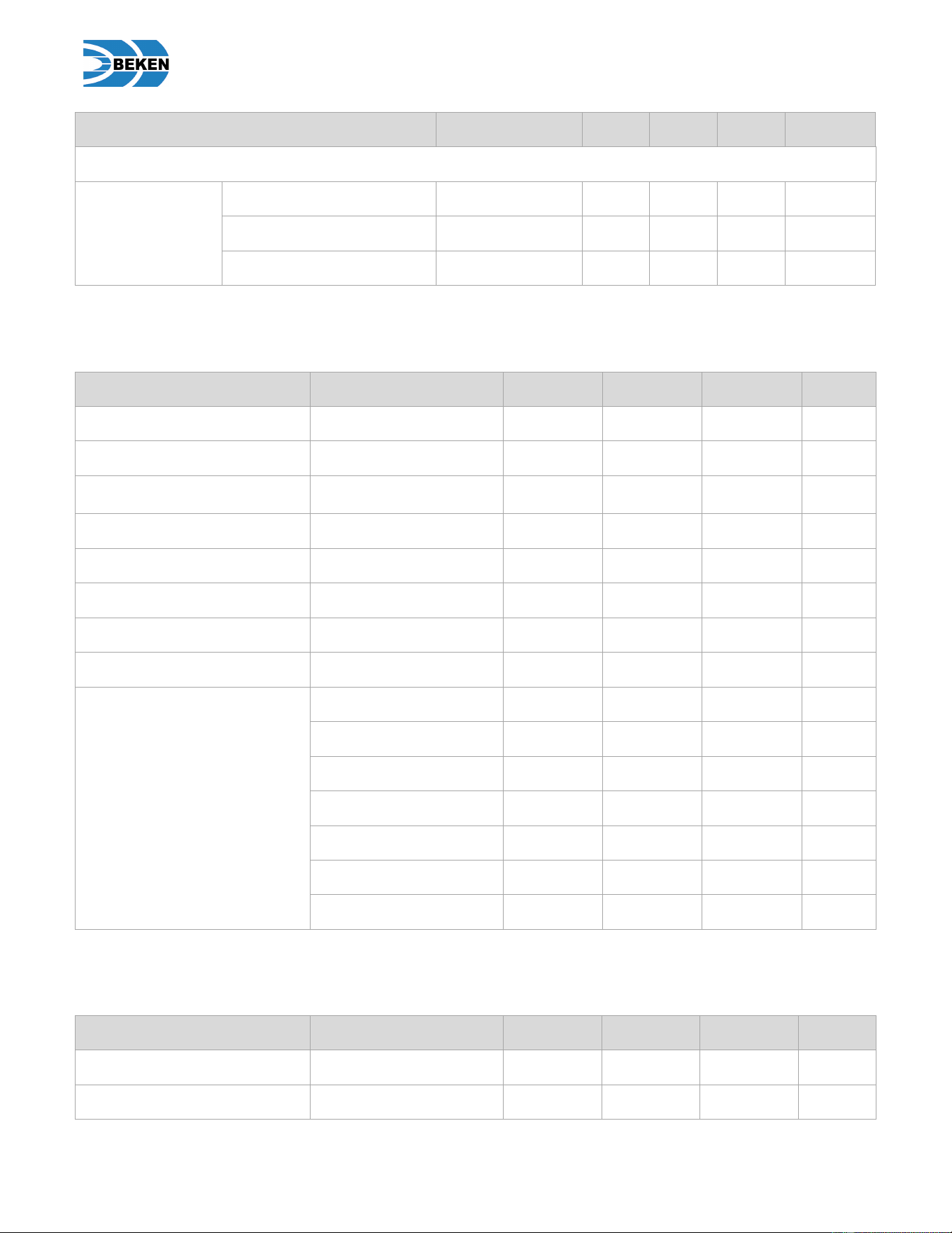
Bluetooth LE 125 kbps
In-band emissions
±2 MHz offset - - -47 - dBm
±3 MHz offset - - -49 - dBm
>±3 MHz offset - - -50 - dBm
Modulation
characteristics
Δf1avg -
-
245
-
kHz
Δf1max - - 246 - kHz
Carrier frequency
offset and drift
Max |f
n
|
n = 0, 1, 2, 3…k
- - 1.5
-
kHz
Max |f
0
– f
n
|
n = 1, 2, 3…k
- - 1.5
-
kHz
|f
0
– f
3
|
- - 1.5
-
kHz
|f
n
– f
n-3
|
n = 7, 8, 9…k
- - 1.5
-
kHz/48 μs
Electrical Characteristics
© 2026 Beken Corporation 21 DS-BKSG2-MINI-E03 V1.2
Parameter
Condition
Min.
Typ.
Max.
Unit
Bluetooth LE 500 kbps
In-band emissions
±2 MHz offset -
-
-47
-
dBm
±3 MHz offset -
-
-49
-
dBm
>±3 MHz offset -
-
-50
-
dBm
4.12 AUX ADC Characteristics
Parameter
Condition Min.
Typ.
Max.
Unit
Conversion clock
- -
-
13
MHz
Conversion time
-1*11( -
16
-
Cycle
V
REF
Internal
-
1.2
-
V
Input voltage range
- 0
-
VBAT
V
Input impedance
-
10
-
-
MΩ
Input capacitance (Cs)
-
-
1
-
pF
DNL
-
-1
-
3
LSB
INL
-
-5
-
5
LSB
Precision
Internal (> 500 mV)
-
-
1
%
Internal (400–500 mV)
-
2
4
%
Internal (300–400 mV)
-
3
6
%
Internal (200–300 mV)
-
-
8
%
Internal (100–200 mV)
-
-
20
%
Internal (50–100 mV)
-
-
40
%
Internal (<50 mV)
-
-
100
%
4.13 I2C Characteristics
Parameter
Condition Min.
Typ.
Max.
Unit
Clock
-
-
-
400
kHz
Pull-up resistor
-
1.5
4.7
10
kΩ

Electrical Characteristics
© 2026 Beken Corporation 22 DS-BKSG2-MINI-E03 V1.2
Parameter
Condition
Min.
Typ.
Max.
Unit
Capacitive load drive strength
(enhanced drive mode)
Ceramic capacitor added to
ground
20
-
-
nF
4.14 PWM Characteristics
Parameter
Condition Min.
Typ.
Max.
Unit
Frequency
- -
-
8
MHz
Recommended pull-down resistor
- -
51
-
KΩ
4.15 NTC Characteristics
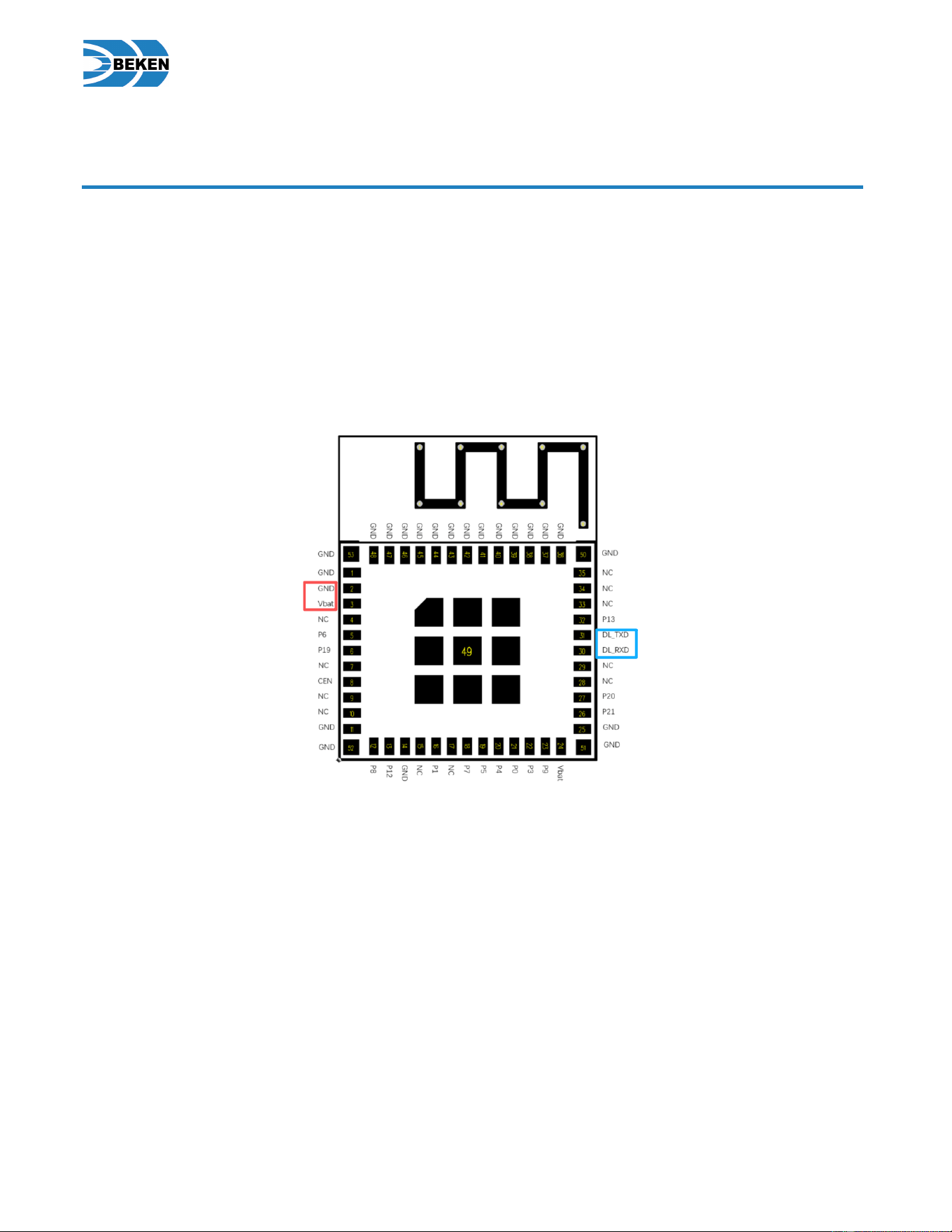
The SOC of BKSG2-MINI includes a temperature sensor (NTC) which, after calibration, can provide chip temperature
detection with an accuracy better than ±5°C.
Module Burning and Test Mode
© 2026 Beken Corporation 23 DS-BKSG2-MINI-E03 V1.2
5. Module Burning and Test Mode
5.1 Firmware Download
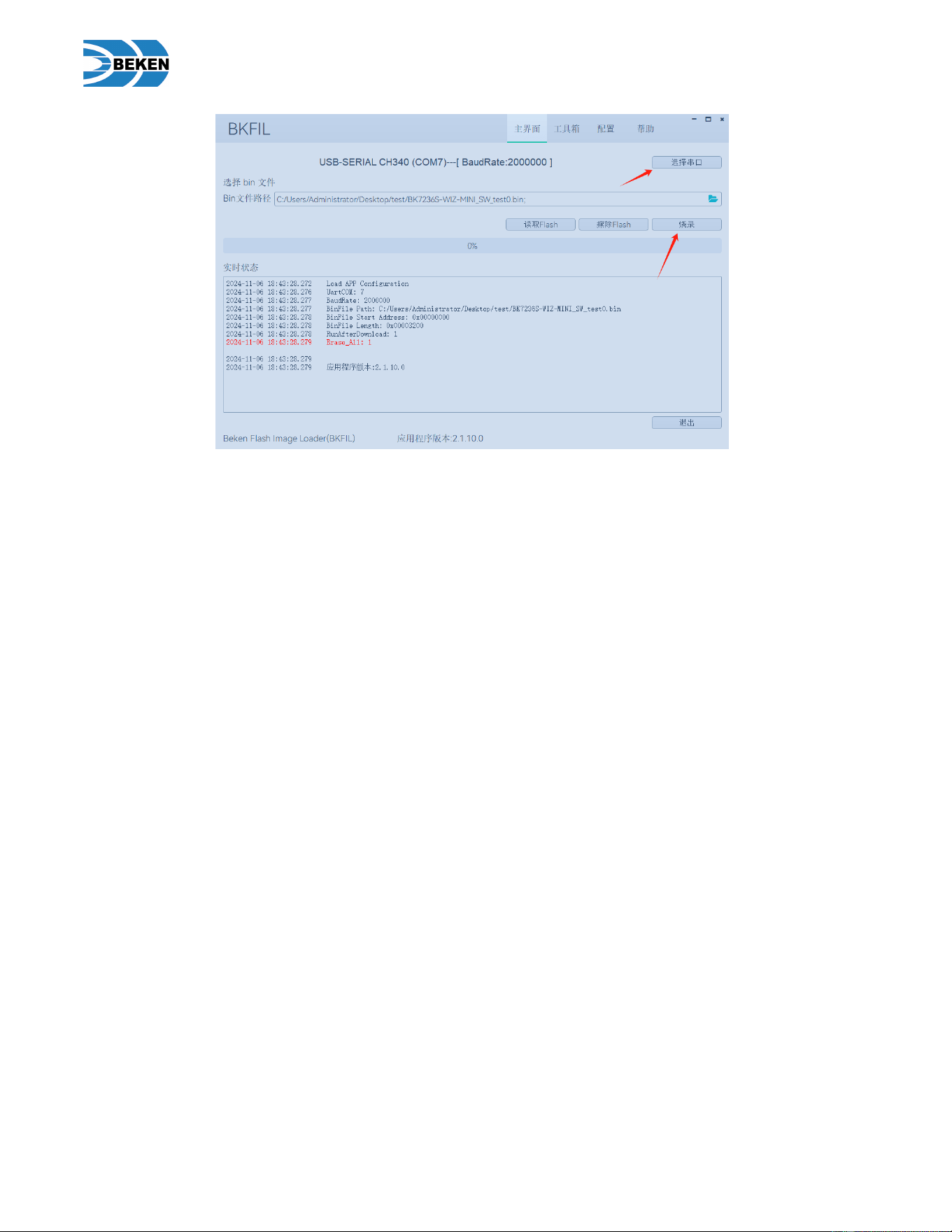
The BK7236-MINI module supports firmware download via UART. Within 5 ms after the chip is powered on, the
downloader sends a handshake command to complete the interaction and then the firmware can be downloaded. The specific
operation method is as follows:
1. Connect the GND, DL_RXD, DL_TXD signal lines of the module to the download tool, and do not supply power to
VBAT for the time being.
2. Open the PC download tool, select the serial port and firmware path, and start burning (the tool also supports script
calls).
Module Burning and Test Mode
© 2026 Beken Corporation 24 DS-BKSG2-MINI-E03 V1.2
3. Supply power to VBAT to start firmware burning.
5.2 Enter Test Mode
During the power-on initialization phase, the module will determine whether the DL_TXD pin is pulled low externally
(usually connected to GND through a 1 KΩ resistor). If it is not pulled low, the firmware will start running normally. If it is
pulled low, the program enters the test mode (ATE mode), and non-signaling tests and other operations can be performed.
Packge information and ordering number
© 2026 Beken Corporation 25 DS-BKSG2-MINI-E03 V1.2
6. Packge information and ordering number
6.1 Packge information
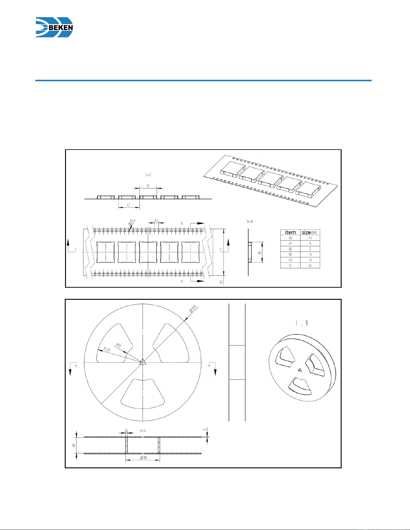
The packaging type of the module is tape reel, the reel width is 48mm, and the diameter is 13 inches with 650 modules per
reel. One packaging box contains 5 reels.

Packge information and ordering number
© 2026 Beken Corporation 26 DS-BKSG2-MINI-E03 V1.2
6.2 Ordering number
The order number of the module is: BKBG2 -MINI-V1.1
Certification
© 2026 Beken Corporation 27 DS-BKSG2-MINI-E03 V1.2
7. Certification
The module has passed the following certifications:
• FCC
• WFA
• BQB
Notes:
•
Due to the optimization of chip and module design, module parameters may change. Please pay attention to the update
of the module datasheet.
• During certification, the transmit power is appropriately adjusted due to the specific application and certification
requirements.
• Test conditions for RF transceiver performance: supply voltage = 3.3 V, ambient temperature = 25 °C.
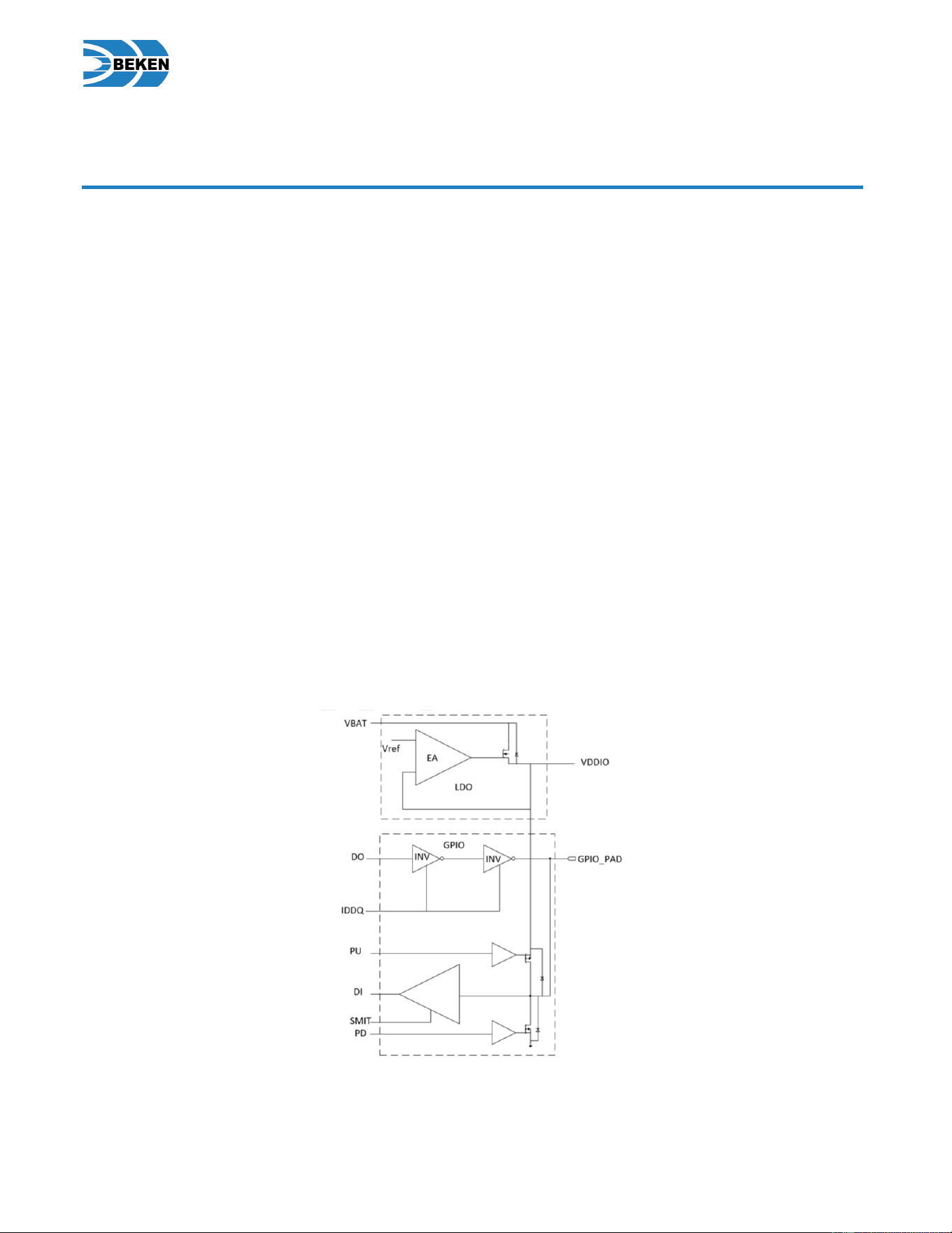
• All GPIOs of the BK7236S have protection diodes for VDDIO and GND, and the structure is shown in the figure
below. When the module does not supply power to Vbat, if the GPIO has a high level with strong drive strength, the
chip will be in a powered operation state. The specific operation is related to the drive strength of the high level on the
GPIO. In order to prevent abnormal operation of the chip, when Vbat is not powered, the voltage applied to the GPIO
is limited to 1.8 V and the drive strength is limited to 2 mA(Equivalent to connecting a 1K resistor in series).
Figure 7-1 Structure of GPIO Protection Diode

Contents
© 2026 Beken Corporation 28 DS-BKSG2-MINI-E03 V1.2
7.1 Revision History
Version
Date Description
1.0
2026/1/5 Initial release
1.1
2026/5/11
Added the connection from module PIN21 to chip PIN16.
1.2
2026/5/19
Add a description of the pin's alternate function. NTC function and
accuracy.

Copyright
© 2026 Beken Corporation. The term “Beken” refers to Beken Corporation and/or its affiliates. This document contains
information that is proprietary to Beken. Any unauthorized use, reproduction, or disclosure of this document in whole or in
part is prohibited.
Disclaimer
The documentation is provided on an "as-is" basis only. Beken reserves the right to make any updates, corrections and any
other modifications to its documentation without further notice and limitation to product information, descriptions, and
specifications herein. Beken does not give warranties as to the accuracy or completeness of the included information. Beken
shall have no liability for any use of the information in this documentation. You should obtain the latest relevant information
before placing orders and should verify that such information is current and complete. Information published by Beken
Use of such information may require a license from a third party under the intellectual property rights of such third party, or
a
regarding any third-party products does not constitute a license to use such products or a warranty or endorsement thereof.
license from Beken under the intellectual property rights of Beken.
Trademarks
Beken, the BEKEN logo, and combinations thereof are trademarks or registered trademarks of Beken. All other product or
brand names mentioned herein are trademarks or registered trademarks of their respective holders.
Beken Corporation
Building 41, 1387 Zhangdong Rd
Shanghai 201203
China
http://www.bekencorp.com

This module is intended for OEM integrators only. Per FCC KDB 996369 D03 OEM
Manual v01 guidance, the following conditions must be strictly followed when using
this certified module:
KDB 996369 D03 OEM Manual v01 rule sections:
2.3 Summarize the specific operational use conditions
The module is tested for standalone mobile RF exposure use condition. Any other
usage conditions such as co-location with other transmitter(s) or being used in a
portable condition will need a separate reassessment through a class II permissive
change application or new
2.2 List of applicable FCC rules This module has been tested for compliance to FCC
part15.247
certification.
2.6 RF exposure considerations This equipment complies with FCC mobile radiation
exposure limits set forth for an uncontrolled environment. This equipment should be
installed and operated with a minimum distance of 20cm between the radiator &
your body. If the module is installed in a portable host, a separate SAR evaluation is
2.4 Single module procedures The EUT was tested inside a specific platform (model:
SmartCore 100)and Single modular app roval for this specific
platform.
2.5 Antenna : PCB Antenna;
Antenna designs Not applicable
required to confirm compliance with relevant FCC portable RF exposure rules.
2.8 Label and compliance information
The final end product must be labeled in a visible area with the following: “Contains
FCC ID:
2BWNW-BKSG2-MINI
”. The grantee'sFCC ID can be used only when all FCC
2.7 Antennas
The following antennas have been certified for use with this module; antennas of the
same type with equal or lower gain may also be used with this module. The antenna
must be installed such that 20 cm can be maintained between the antenna and
users. Antenna Type Antenna : PCB Antenna;
compliance requirements are met.
2.9 Information on test modes and additional testing requirements
This transmitter is tested in a standalone mobile RF exposure condition and any co-
located or simultaneous transmission with other transmitter(s) or portable use will
require a separate class II permissive change re-evaluation or new certification.
2.10 Additional testing, Part 15 Subpart B disclaimer
This transmitter module is tested as a subsystem and its certification does not cover
the FCC Part 15 Subpart B (unintentional radiator) rule requirement applicable to the
final host. The final host will still need to be reassessed for compliance to this portion
of rule requirements if applicable.
FCC Warning
This device complies with Part 15 of the FCC Rules. Operation is subject to the following two
conditions:
(1) This device may not cause harmful interference, and (2) this device must accept any
interference received, including interference that may cause undesired operation.
NOTE 1: Any changes or modifications to this unit not expressly approved by the party
responsible for compliance could void the user's authority to operate the equipment.
FCC Radiation Exposure Statement:
This equipment complies with FCC radiation exposure limits set forth for an uncontrolled
environment. End users must follow the specific operating instructions for satisfying RF exposure
compliance.
This module certified that complies with RF exposure requirement under mobile or fixed condition
, this module is to be installed only in mobile or fixed applications.
A mobile device is defined as a transmitting device designed to be used in other than fixed
locations and to generally be used in such a way that a separation distance of at least 20
centimeters is normally maintained between the transmitter's radiating structure(s) and the body of
the user or nearby persons. Transmitting devices designed to be used by consumers or workers that
can be easily re-located, such as wireless devices associated with a personal computer, are
considered to be mobile devices if they meet the 20 centimeter separation requirement.
A fixed device is defined as a device is physically secured at one location and is not able to be
easily moved to another location.
Note 2: Any modifications made to the module will void the Grant of Certification, this module is
limited to OEM installation only and must not be sold to end-users, end-user has no manual
instructions to remove or install the device, only software or operating procedure shall be placed in
the end-user operating manual of final products.
Note 3: Additional testing and certification may be necessary when multiple modules are used.
Note 4: The module may be operated only with the antenna with which it is authorized. Any
antenna that is of the same type and of equal or less directional gain as an antenna that is
authorized with the intentional radiator may be marketed with, and used with, that intentional
radiator.

