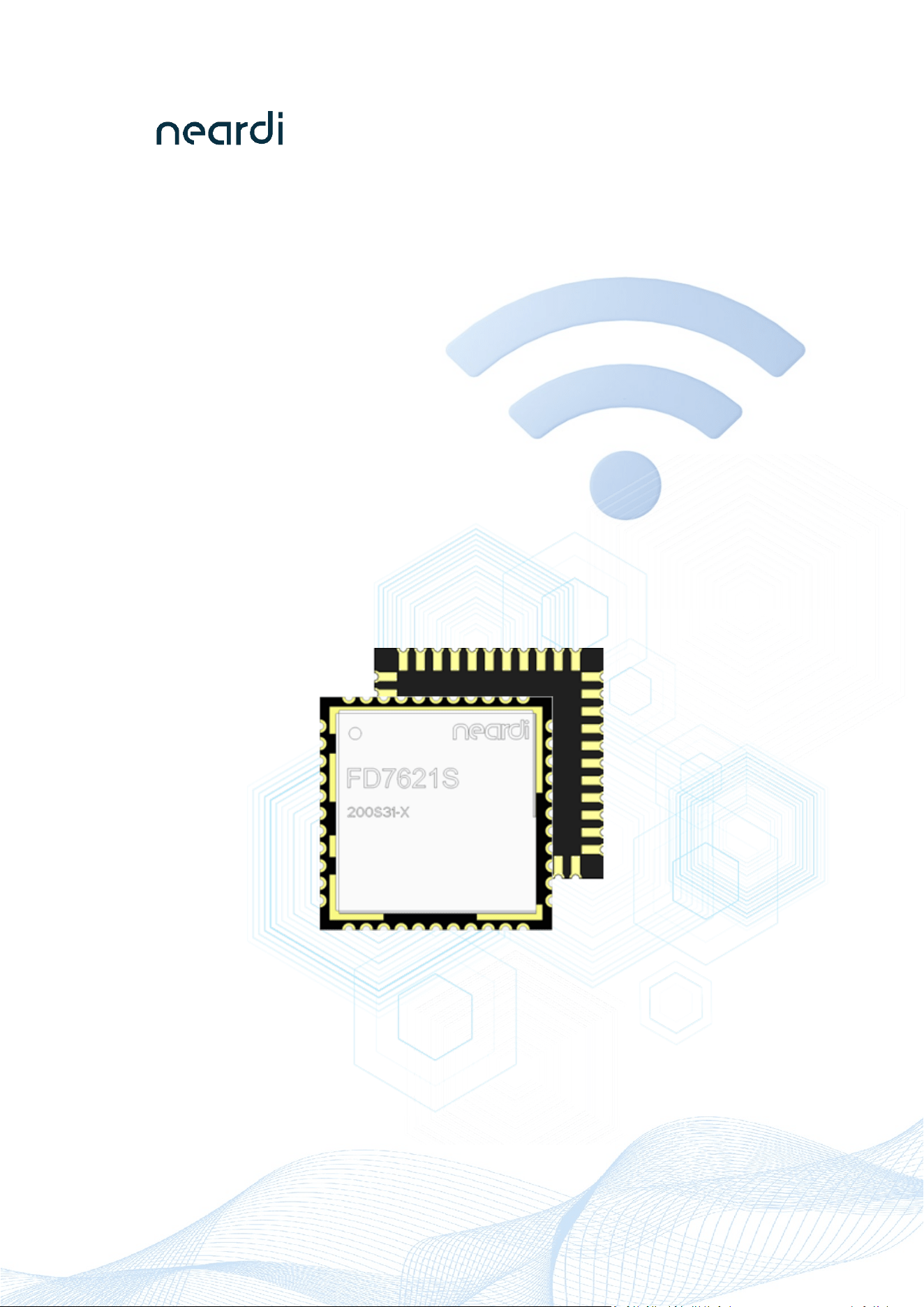
FD7621S WIFI Module
Datasheet
V1.0
Shanghai Neardi Technology Co., Ltd.
www.neardi.com

FD7621S
Neardi Technology www.neardi.com
1 /
Shanghai Neardi Technology Co., Ltd. (referred to as "Neardi Technology") always adheres to the
customer-first service tenet and provides customers with fast and efficient support services. If
you have any needs, please feel free to contact our company, the contact information is as
follows:
Shanghai Neardi Technology Co., Ltd.
www.neardi.com
Tel: +86 21 20952021
Email: sales@neardi.com
Introduction
Neardi Technology provides this document for customers to use as a reference for product design and terminal
applications. It is recommended that customers confirm the specifications and parameters provided in the
document in detail, and confirm whether it can meet the design or application of the required products. At the
same time, it is strongly recommended that customers do detailed tests in actual application scenarios based on
the samples provided by our company to ensure that they meet the end use requirements. Neardi Technology is
not responsible for any damages suffered due to the use of documents, materials and product functions.
The relevant parameters or design charts in this document are only examples, and customers should base their
own independent analysis, evaluation and judgment when designing or using terminal products. Before
customers use any design or service guided by this document, please read this statement carefully, understand
and agree that although Neardi Technology has taken reasonable commercial efforts to provide the best possible
experience, this document and its contents are PROVIDED TO YOU ON AN "AS AVAILABLE" BASIS. The information
in this document is subject to change without notice.
Agreement
Unless specifically authorized by Neardi Technology, the recipient of the product documentation, hardware
reference drawings, software descriptions and other materials provided by our company must keep the received
content confidential and shall not use it for any other purpose other than the implementation and development
of this project.
Copyright Statement
Documents and information provided by our company may not be obtained, used or disclosed to third parties, or
such copyrighted materials may be copied, reproduced, plagiarized, published, displayed, translated, distributed
or merged, modified or created derivative works unless obtain prior written consent. Neardi Technology has
exclusive rights to copyrighted materials and does not grant or convey a license to any patent, copyright,
trademark or service mark rights, and no purchase of any kind shall be deemed to be the grant of a license.
Neardi Technology has the right to pursue legal responsibility for any illegal infringements that violate
confidentiality, use without authorization or maliciously use the documents and information in other illegal
forms.
© 2023 Shanghai Neardi Technology Co., Ltd. All Rights Reserved.

FD7621S
Neardi Technology www.neardi.com
2 /
Version History
Version Date Illustrate
V1.0 2026/3/13 Initial Version

FD7621S
Neardi Technology www.neardi.com
3 /
Contents
1 Product Overview .......................................................................................................................... 4
1.1 Product Introduction ........................................................................................................... 4
1.2 Wi-Fi Characteristics ............................................................................................................ 5
1.3 Bluetooth Characteristics .................................................................................................... 5
1.4 Block Diagram ..................................................................................................................... 6
1.5 Parameters .......................................................................................................................... 6
2 Pin Definition ................................................................................................................................. 7
2.1 Pin Number ......................................................................................................................... 7
2.2 Pin Description .................................................................................................................... 7
3 Mechanical Specifications ............................................................................................................. 9
3.1 Mechanical Dimensions ...................................................................................................... 9
3.2 Recommended PCB Layout Footprint ................................................................................. 9
4 Electrical Performance and Reliability ......................................................................................... 10
4.1 Absolute Maximum Voltage Range ................................................................................... 10
4.2 Recommended Operation Conditions ............................................................................... 10
4.3 Power On/Off Sequence.................................................................................................... 10
4.4 Reliability ........................................................................................................................... 11
5 Interface Timing Parameters ....................................................................................................... 12
5.1 SDIO Interface Timing........................................................................................................ 12
5.2 PCM Interface Timing ........................................................................................................ 15
6RF Characteristics
.......................................................................................................................... 16
6.1 2.4GHZ Wi-Fi Radio Frequency (RF) Characteristics .......................................................... 16
6.3 Bluetooth Radio Frequency (RF) Characteristics ............................................................... 19
7Hardware Design Guide ................................................................................................................ 21
7.1 Power Design Notice ......................................................................................................... 21
7.2 Interface Design Notice ..................................................................................................... 22
8 Storage,Production and Packaging ............................................................................................... 24
8.1 Storage Conditions ............................................................................................................ 24
8.2 Production Welding ........................................................................................................... 24
8.3 Packing Specifications ....................................................................................................... 25
FD7621S
Neardi Technology www.neardi.com
4 /
1 Product Overview
1.1 Product Introduction
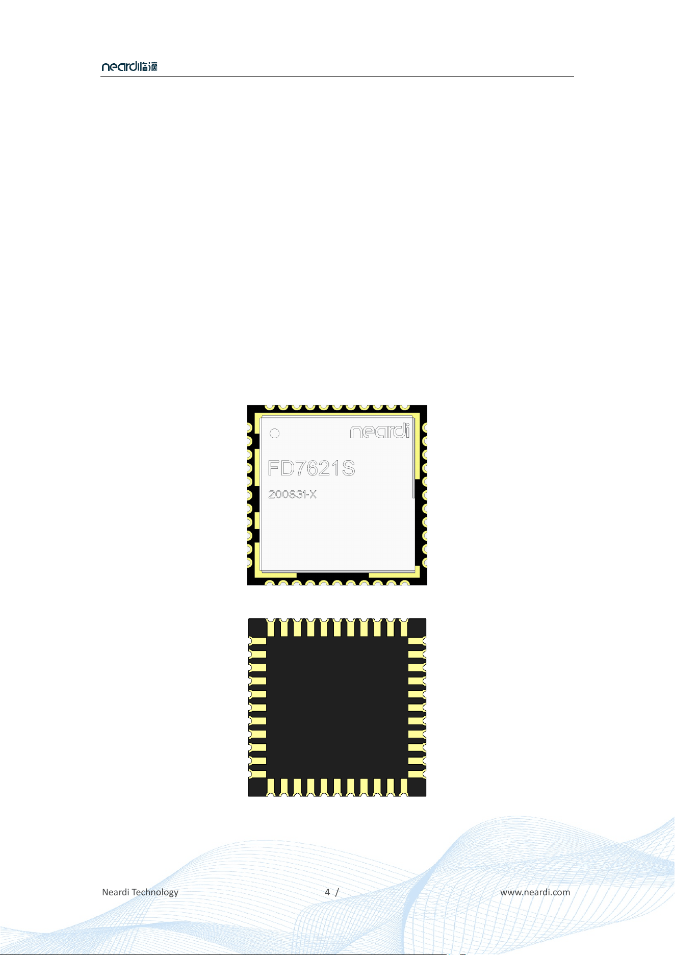
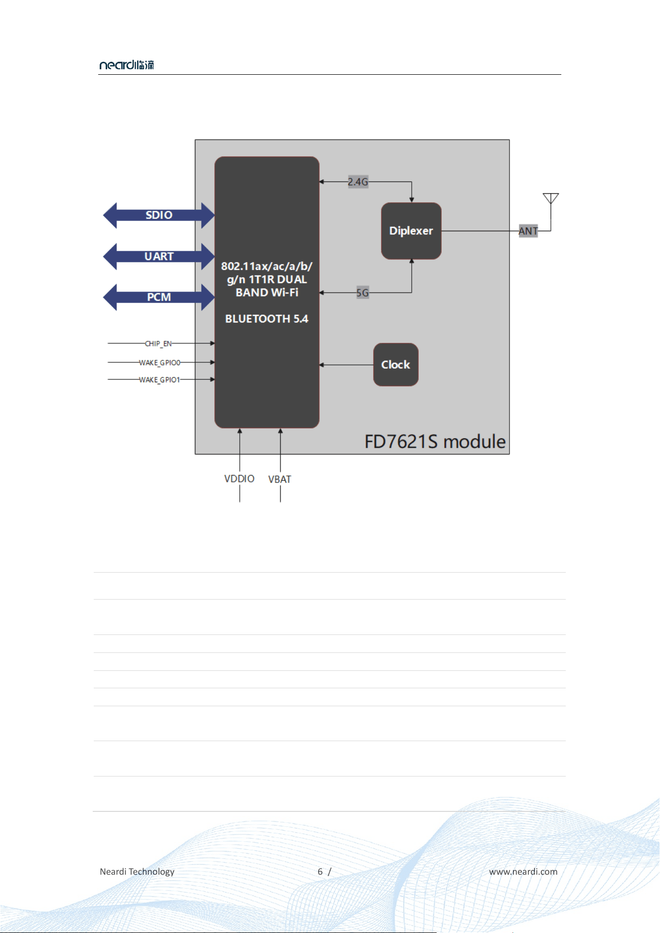
FD7621S is a highly integrated, low-cost combo module with high-performance and
low-power. It supports Wi-Fi 6 and Bluetooth 5.4 protocol, supports Wi-Fi MAC of the final
version of Wi-Fi 6 Wave2 protocol, Wi-Fi Baseband of 1T1R, and high-performance RF. It also
supports SDIO3.0, HS-UART and PCM interfaces for connection with the Host. This module also
supports BT and Wi-Fi to work in coexistence mode. It is suitable for consumer electronics such
as IPC, tablet and IOT, and can also be used in fields with high reliability requirements such as
industrial interconnection.

FD7621S
Neardi Technology www.neardi.com
5 /
1.2 Wi-Fi Characteristics
IEEE 802.11a/b/g/n/ac/ax (supports wave-2) wireless LAN communication protocol
IEEE 802.11 d/e/h/i/k/mc/r/v/w
Phy rate up to 600.5Mbps, Throughput rate up to 520Mbps
Multiple modes such as Wi-Fi STA, AP, and P2P
2.4G 40MHZ, 5G 80MHz bandwidth, 1T/1R
Up to 1024QAM modulation, supports LDPC and STBC
UL/DL OFDMA, DL MU-MIMO
QoS, WFA WMM, WMM PS
RSSI and CSI Reporting
Beamformee and 4*1 Tx Beamforming
WPA, WPA2, WPA3 encryption and decryption, WAPI and WPS2.0
ER, DCM to improve transceiver gain
20in40/80/160, 80in160 HE PPDU, Partial band MU MIMO to improve air interface
utilization;
BSS Color, Spatial Reuse to improve air interface utilization
TWT, Intra-PPDU PS, VHT TXOP PS to optimize dynamic power consumption in small
bandwidth and multi-BSS environment
1.3 Bluetooth Characteristics
Support Bluetooth (Classic BT+BLE) v2.1, v3.0, v4.2, v5.4 features
SDIO interface for BT data transmission
PCM/IIS interface for audio transmission
BR/EDR/LE 1M/LE 2M/LE LR
Support sco and esco link
SSP/Secure Connection
Low power mode (sniff, sniff sub-rating)
Support BT/Wi-Fi coexistence
FD7621S
Neardi Technology www.neardi.com
6 /
1.4 Block Diagram
1.5 Parameters
Product Name FD7621S
Product
description
802.11ax/ac/a/b/g/n 1T1R dual band Wi-Fi and Bluetooth 5.4 comb module
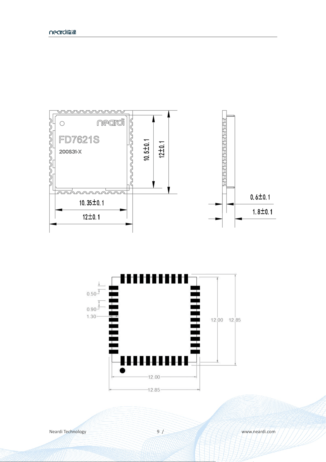
Dimension 12.0(±0.1)mm*12.0(±0.1)mm*1.8(±0.1)mm
Power supply VBAT:3.0~3.6V;VDDIO:1.62V~1.92V/3.0V~3.6V
Host interface SDIO3.0 + UART + PCM
Footprint LCC 44pin
Operating
temperature
-30°C to 70°C
Operating
humidity
10% to 90% (Non-Condensing)
Storage
temperature
- 40°C to 85°C
FD7621S
Neardi Technology www.neardi.com
7 /
2 Pin Definition
2.1 Pin Number
2.2 Pin Description
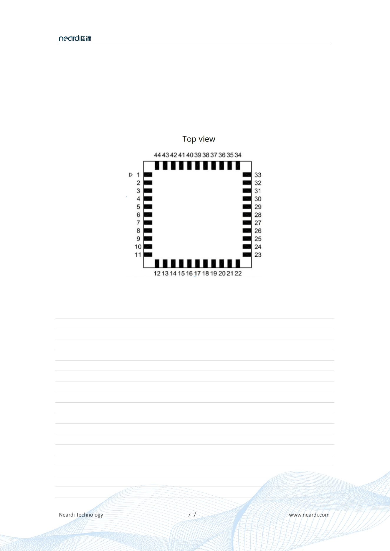
Pin Number Pin Name Pin Type Pin Description
1
GND
G
Ground connections
2
WL_BT_ANT
RF
Wi-Fi & BT antenna I/O port
3
GND
G
Ground connections
4
NC
-
Floating (Don’t connected to ground)
5
NC
-
Floating (Don’t connected to ground)
6
NC
-
Floating (Don’t connected to ground)
7
NC
-
Floating (Don’t connected to ground)
8
GND
-
Ground connections
9
VBAT
P
Main power voltage source input
10
NC
-
Floating (Don’t connected to ground)
11
NC
-
Floating (Don’t connected to ground)
12
CHIP_EN
I
Module enable signal
13
WAKE_GPIO0
I/O
Wake up signal with auto negotiation
14
SDIO_DATA_2
I/O
SDIO data line 2
15
SDIO_DATA_3
I/O
SDIO data line 3
16
SDIO_DATA_CMD
I/O
SDIO command line

FD7621S
Neardi Technology www.neardi.com
8 /
17
SDIO_DATA_CLK
I/O
SDIO clock line
18
SDIO_DATA_0
I/O
SDIO data line 0
19
SDIO_DATA_1
I/O
SDIO data line 1
20
GND
G
Ground connections
21
NC
-
Floating (Don’t connected to ground)
22
VDDIO
P
I/O Voltage supply input
23
NC
-
Floating (Don’t connected to ground)
24
NC
-
Floating (Don’t connected to ground)
25
PCM_OUT
O
PCM Data output
26
PCM_CLK
I/O
PCM clock
27
PCM_IN
I
PCM data input
28
PCM_SYNC
I/O
PCM sync signal
29
NC
-
Floating (Don’t connected to ground)
30
NC
-
Floating (Don’t connected to ground)
31
GND
G
Ground connections
32 NC -
Floating (Don’t connected to ground)
33 GND G
Ground connections
34 WAKE_GPIO1 I/O
Wake up signal with auto negotiation
35 NC -
Floating (Don’t connected to ground)
36 GND G
Ground connections
37 NC -
Floating (Don’t connected to ground)
38 NC -
Floating (Don’t connected to ground)
39 NC -
Floating (Don’t connected to ground)
40 NC -
Floating (Don’t connected to ground)
41 UART_RTS_N I/O
UART DCE request send signal
42 UART_TXD I/O
UART TX signal
43 UART_RXD I/O
UART RX signal
44 UART_CTS_N I/O
UART DEC clear send signal
FD7621S
Neardi Technology www.neardi.com
9 /
3 Mechanical Specifications
3.1 Mechanical Dimensions
3.2 Recommended PCB Layout Footprint
FD7621S
Neardi Technology www.neardi.com
10 /
4 Electrical Performance and Reliability
4.1 Absolute Maximum Voltage Range
Symbol Description Min Max Unit
VBAT Power Supply Voltage -0.5 5.0
*
V
VDDIO Digital/Bluetooth/SDIO/ I/O Voltage -0.5 5.0
*
V
* If the voltage exceeds this value, the chip will be irreversibly damaged.
4.2 Recommended Operation Conditions
Symbol Description Min Type Max Unit
Ta Ambient Operating Temperature -30 25 70 ℃
Antenna External Antenna VSWR
1.92:1 2:01
VBAT Power Supply Voltage 3 3.3 3.6 V
Power Supply Current - 500 1000 mA
VDDIO I/O Voltage
1.62 1.8 1.92 V
3 3.3 3.6 V
Supply Current
- - 100 mA
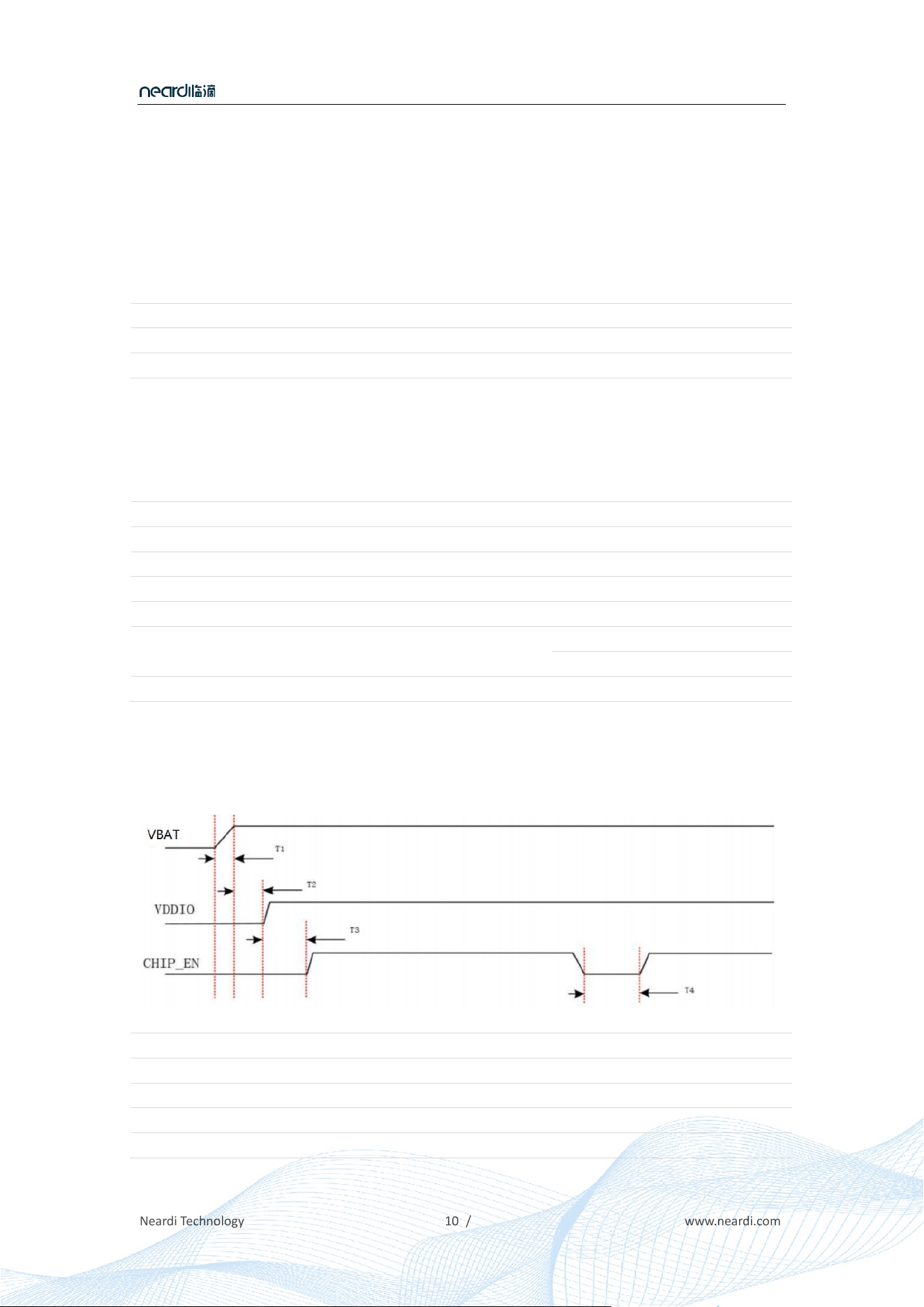
4.3 Power On/Off Sequence
Symbol Description Min Type Max Unit
1 VBAT Ramp up time 0.2 0.5 - mS
2 VDDIO should be powered on after VBAT is powered on 0 - - mS
3 CHIP_EN should be powered on after VDDIO is powered on 0 - - mS
4 CHIP_EN reset time 50 - - mS
FD7621S
Neardi Technology www.neardi.com
11 /
4.4 Reliability
Item Test Model Class Level Criteria
ESD
HBM 2 2000V
ANSI/ESDA/JEDEC
JS-001-2017
CDM C2a 500V
ANSI/ESDA/JEDEC
JS-002-2018
Latch-up
Current II A 200mA
JEDEC STANDARD NO.78F
JANUARY 2022
Voltage II A 1.5xVmax
JEDEC STANDARD NO.78F
JANUARY 2022
FD7621S
Neardi Technology www.neardi.com
12 /
5 Interface Timing Parameters
5.1 SDIO Interface Timing
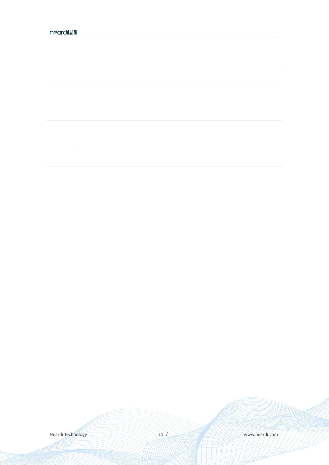
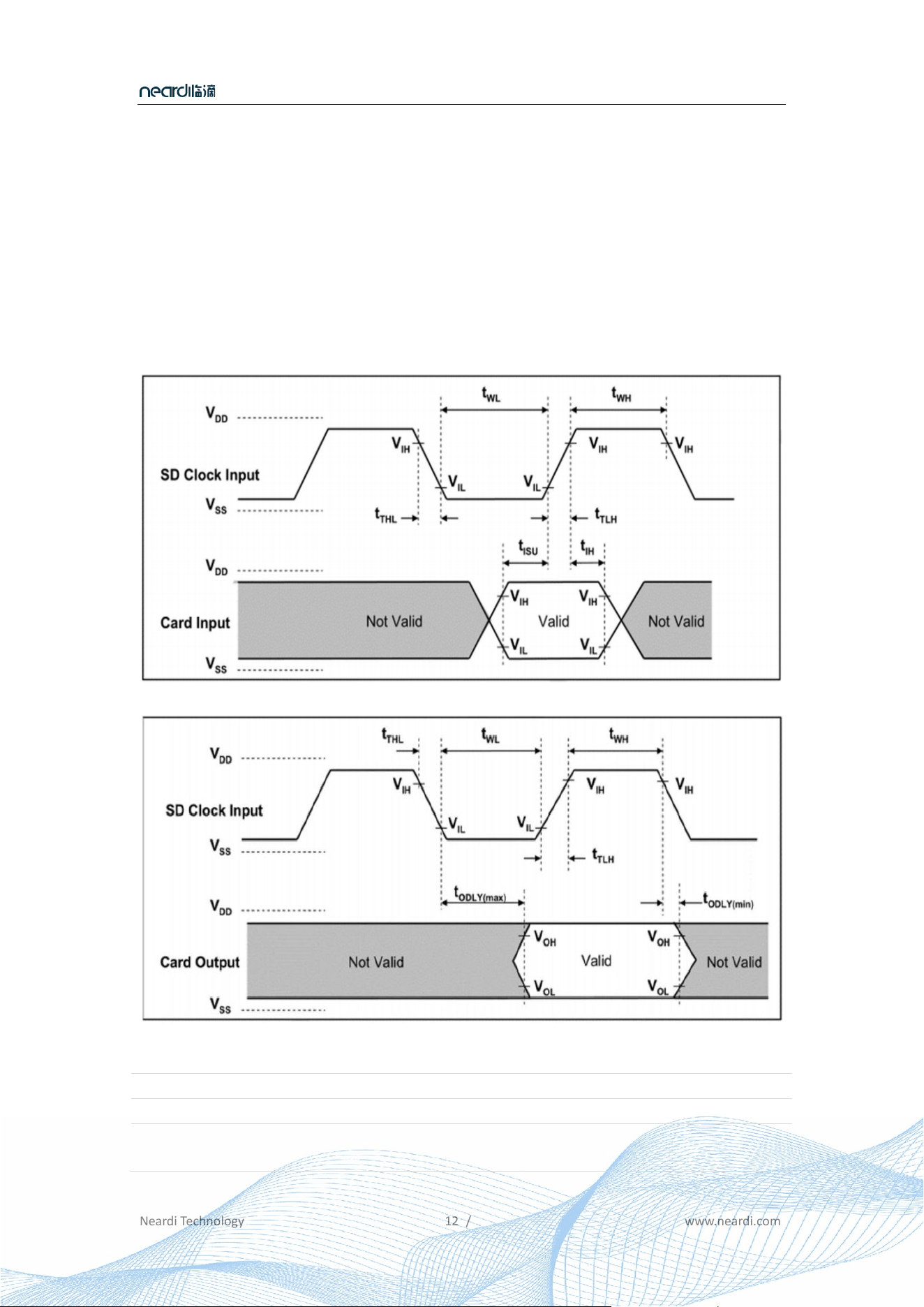
5.1.1 Default Speed Mode
SDIO device input timing(Default Speed Mode)
SDIO device output timing (Default Speed Mode)
Parameter Symbol Min Max Unit Remark
Clock
Clock Freq Data Transfer Mode fPP 0 25 MHZ Cload ≤ 10 pF
FD7621S
Neardi Technology www.neardi.com
13 /
Clock Freq Identification Mode fO 0 400 KHZ Cload ≤ 10 pF
Clock low time wxya 10
ns Cload ≤ 10 pF
Clock high time tWH 10
ns Cload ≤ 10 pF
Clock rise time tTLH
10 ns Cload ≤ 10 pF
Clock fall time tTHL
10 ns Cload ≤ 10 pF
Inputs CMD,DAT(referenced to CLK)
Input set-up time tISU 5
ns Cload ≤ 10 pF
Input hold time tIHU 5
ns Cload ≤ 10 pF
Outputs CMD,DAT(referenced to CLK)
Output Delay time during Data
Transfer Mode
tODLY 0 14 ns Cload ≤ 40 pF
Output Delay time during
Identification Mode
tODLY 0 50 ns Cload ≤ 40 pF
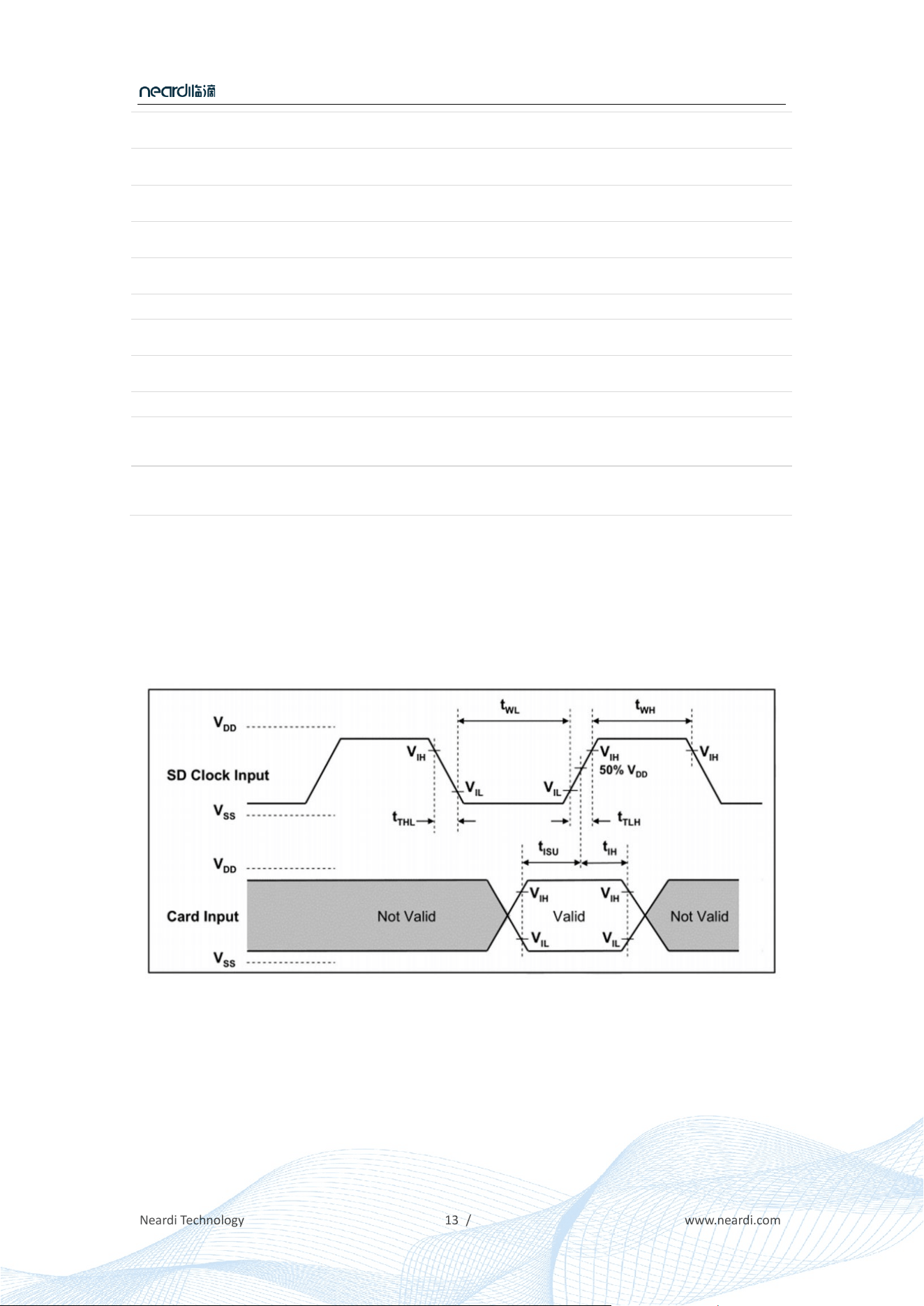
5.1.2 High-Speed Mode
SDIO device input timing (High Speed Mode)
FD7621S
Neardi Technology www.neardi.com
14 /
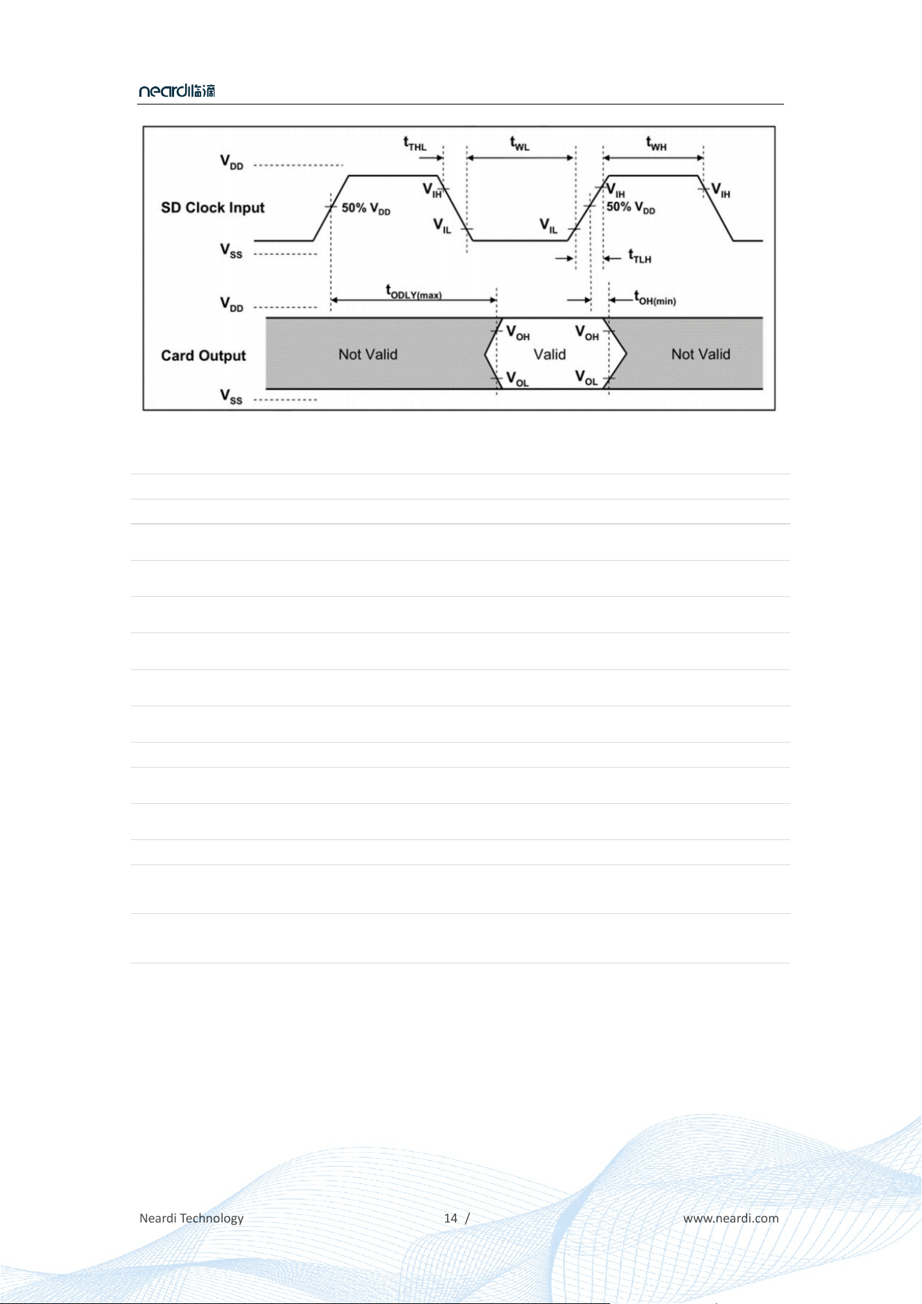
SDIO device output timing (High Speed Mode)
Parameter Symbol Min Max Unit Remark
Clock
Clock Freq Data Transfer Mode fPP 0 50 MHZ Cload ≤ 10 pF
Clock Freq Identification Mode fO 0 400 KHZ Cload ≤ 10 pF
Clock low time wxya 7
ns Cload ≤ 10 pF
Clock high time tWH 7
ns Cload ≤ 10 pF
Clock rise time tTLH
3 ns Cload ≤ 10 pF
Clock fall time tTHL
3 ns Cload ≤ 10 pF
Inputs CMD,DAT(referenced to CLK)
Input set-up time tISU 6
ns Cload ≤ 10 pF
Input hold time tIHU 2
ns Cload ≤ 10 pF
Outputs CMD,DAT(referenced to CLK)
Output Delay time during Data
Transfer Mode
tODLY 0 14 ns Cload ≤ 4 0 pF
Output Delay time during
Identification Mode
tODLY 2.5
ns Cload ≤ 15 pF
FD7621S
Neardi Technology www.neardi.com
15 /
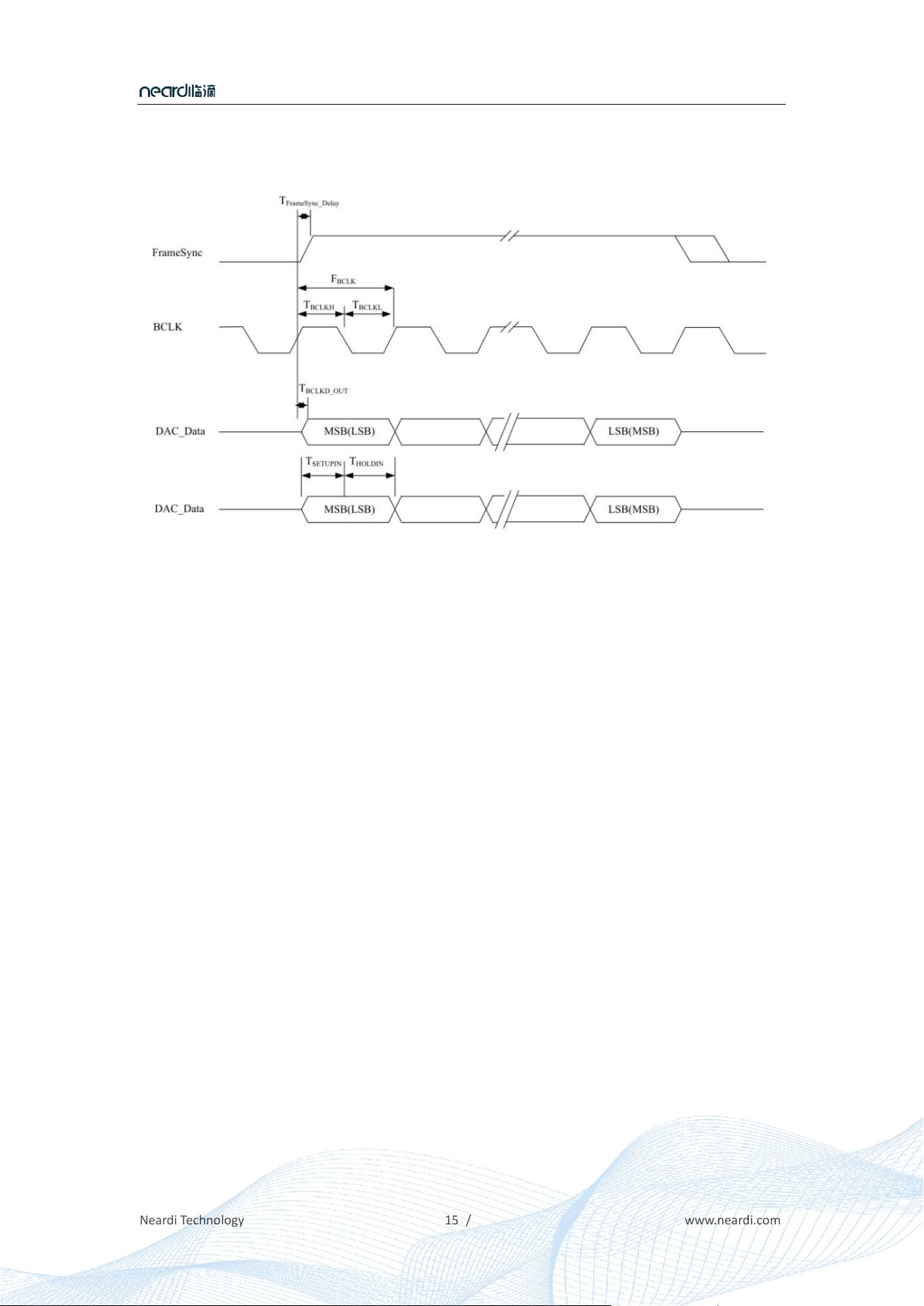
5.2 PCM Interface Timing
PCM Bus Timing
FD7621S
Neardi Technology www.neardi.com
16 /
6 RF Characteristics
6.1 2.4GHZ Wi-Fi Radio Frequency (RF) Characteristics
Conditions: VBAT=3.3V; VDDIO=1.8V; Ta:25℃
Features Description
Wi-Fi Standard IEEE 802.11b/g/n/ac/ax
Frequency Range 2.4~2.4835GHz(2.4GHz ISM Band)
Channels Ch1~Ch13
Modulation
802.11b (DSSS): CCK, DQPSK, DBPSK;
802.11g (OFDM): BPSK, QPSK, QAM16, QAM64;
802.11n (OFDM): BPSK, QPSK, QAM16, QAM64;
802.11ac (OFDM): BPSK, QPSK, QAM16, QAM64, QAM256;
802.11ax (OFDMA): BPSK, BPSK_DCM, QPSK, QPSK_DCM, QAM16,
QAM16_DCM, QAM64, QAM256, QAM1024;
Date Rate
802.11b: 1, 2, 5.5, 11Mbps;
802.11g: 6, 9, 12, 18, 24, 36, 48, 54Mbps;
802.11n (HT20): MCS0~MCS7 6.5~72.2Mbps;
802.11n (HT40): MCS0~MCS7 13.5~150Mbps;
802.11ac(VHT20): MCS0~MCS8 6.5~86.7Mbps;
802.11ac(VHT40): MCS0~MCS9 13.5~200Mbps;
802.11ax (HE20): MCS0~MCS11 8~143.4Mbps;
802.11ax (HE40): MCS0~MCS11 16~286.8Mbps;
Frequency Tolerance ≤±5ppm
2.4G Transmitter Specifications
Modulation TX Rate
TX
EVM
(dB)
TX
Mask
VBAT
current
(mA)
802.11b 1Mbps ≤35% PASS 413
802.11b 11Mbps ≤35% PASS 253
802.11g 6Mbps ≤-5 PASS 256
802.11g 54Mbps ≤-25 PASS 317
802.11n HT20 MCS0 ≤-5 PASS 251
802.11n HT20 MCS7 ≤-27 PASS 253
802.11n HT40 MCS0 ≤-5 PASS 254
802.11n HT40 MCS7 ≤-27 PASS 231
802.11ac VHT20 MCS0 ≤-5 PASS 247
802.11ac VHT20 MCS8 ≤-30 PASS 220

FD7621S
Neardi Technology www.neardi.com
17 /
802.11ac VHT40 MCS0 ≤-5 PASS 251
802.11ac VHT40 MCS9 ≤-32 PASS 188
802.11ax HE20 MCS0 ≤-5 PASS 224
802.11ax HE20 MCS11 ≤-35 PASS 210
802.11ax HE40 MCS0 ≤-5 PASS 234
802.11ax HE40 MCS11 ≤-35 PASS 150
2.4G Receiver Specifications
Modulation RX Rate
Min
Input
Level
(dBm)
Max
Input
Level
(dBm)
PER
VBAT
current
(mA)
802.11b 1Mbps ≤-96 -5 8% 77.8
802.11b 11Mbps ≤-87 -5 8% 77.8
802.11g 6Mbps ≤-92 -5 10% 80.4
802.11g 54Mbps ≤-75 -5 10% 80.7
802.11n HT20 MCS0 ≤-92 -5 10% 82.8
802.11n HT20 MCS7 ≤-72 -5 10% 84.5
802.11n HT40 MCS0 ≤-89 -5 10% 86.7
802.11n HT40 MCS7 ≤-70 -5 10% 89.7
802.11ac VHT20 MCS0 ≤-91 -5 10% 83.1
802.11ac VHT20 MCS8 ≤-68 -5 10% 84.9
802.11ac VHT40 MCS0 ≤-89 -5 10% 87.2
802.11ac VHT40 MCS9 ≤-63 -5 10% 90.6
802.11ax HE20 MCS0 ≤-92 -5 10% 83.6
802.11ax HE20 MCS11 ≤-60 -5 10% 83.6
802.11ax HE40 MCS0 ≤-89 -5 10% 87.6
802.11ax HE40 MCS11 ≤-58 -5 10% 88.5
6.2 5GHZ Wi-Fi RF Characteristics
Conditions: VBAT=3.3V; VDDIO=1.8V; Ta:25℃
Features Description
Wi-Fi
Standard
IEEE 802.11a/n/ac/ax
Frequency
Range
5.15~5.25GHz; 5.25~5.35GHz; 5.47~5.73GHz; 5.735~5.835GHz (5GHz ISM Band)
Channels Ch36,Ch40, Ch44, Ch48; Ch52~Ch64; Ch100~Ch140; Ch149~Ch165
Modulation
802.11a (OFDM): BPSK, QPSK, QAM16, QAM64;
802.11n (OFDM): BPSK, QPSK, QAM16, QAM64;
802.11ac (OFDM): BPSK, QPSK, QAM16, QAM64, QAM256;
802.11ax (OFDMA): BPSK, BPSK_DCM, QPSK, QPSK_DCM, QAM16, QAM16_DCM, QAM64,
QAM256, QAM1024;

FD7621S
Neardi Technology www.neardi.com
18 /
Date Rate
802.11a: 6, 9, 12, 18, 24, 36, 48, 54Mbps;
802.11n (HT20): MCS0~MCS7: 6.5~72.2Mbps;
802.11n (HT40): MCS0~MCS7: 13.5~150Mbps;
802.11ac (VHT20): MCS0~MCS8: 6.5~86.7Mbps;
802.11ac (VHT40): MCS0~MCS9: 13.5~200Mbps;
802.11ac (VHT80): MCS0~MCS9: 29.3~433.3Mbps;
802.11ax (HE20): MCS0~MCS11: 8~143.4Mbps;
802.11ax (HE40): MCS0~MCS11: 16~286.8Mbps;
802.11ax (HE80): MCS0~MCS11: 34~600.5Mbps;
Frequency
Tolerance
≤±5ppm
5G Transmitter Specifications
Modulation TX Rate TX EVM(dB) TX Mask
VBAT current
(mA)
802.11a 6Mbps ≤-5 PASS 276
802.11a 54Mbps ≤-25 PASS 342
802.11n HT20 MCS0 ≤-5 PASS 273
802.11n HT20 MCS7 ≤-27 PASS 276
802.11n HT40 MCS0 ≤-5 PASS 258
802.11n HT40 MCS7 ≤-27 PASS 232
802.11ac VHT20 MCS0 ≤-5 PASS 273
802.11ac VHT20 MCS8 ≤-30 PASS 242
802.11ac VHT40 MCS0 ≤-5 PASS 258
802.11ac VHT40 MCS9 ≤-32 PASS 186
802.11ac VHT80 MCS0 ≤-5 PASS 256
802.11ac VHT80 MCS9 ≤-32 PASS 285
802.11ax HE20 MCS0 ≤-5 PASS 247
802.11ax HE20 MCS11 ≤-35 PASS 221
802.11ax HE40 MCS0 ≤-5 PASS 243
802.11ax HE40 MCS11 ≤-35 PASS 149
802.11ax HE80 MCS0 ≤-5 PASS 246
802.11ax HE80 MCS11 ≤-35 PASS 267
5G Receiver Specifications
Modulation RX Rate Min Input Level(dBm)
Max Input Level
(dBm)
PER
VBAT current
(mA)
802.11a 6Mbps -91 -5 10% 87.5
802.11a 54Mbps -74 -5 10% 88.1
802.11n HT20 MCS0 -91 -5 10% 90.5
802.11n HT20 MCS7 -71 -5 10% 92.7
802.11n HT40 MCS0 -88 -5 10% 94.1
802.11n HT40 MCS7 -69 -5 10% 98.2
802.11ac VHT20 MCS0 -91 -5 10% 90.9
802.11ac VHT20 MCS8 -67 -5 10% 92.4

FD7621S
Neardi Technology www.neardi.com
19 /
802.11ac VHT40 MCS0 -88 -5 10% 95.6
802.11ac VHT40 MCS9 -63 -5 10% 98.7
802.11ac VHT80 MCS0 -85 -5 10% 102.5
802.11ac VHT80 MCS9 -59 -5 10% 109.2
802.11ax HE20 MCS0 -91 -5 10% 92.1
802.11ax HE20 MCS11 -60 -5 10% 92.5
802.11ax HE40 MCS0 -89 -5 10% 96.7
802.11ax HE40 MCS11 -58 -5 10% 96.6
802.11ax HE80 MCS0 -86 -5 10% 105.3
802.11ax HE80 MCS11 -53 -5 10% 106.5
6.3 Bluetooth Radio Frequency (RF) Characteristics
Conditions: VBAT=3.3V; VDDIO=1.8V; Ta:25℃
Features Description
Bluetooth
Standard
Bluetooth v2.1+EDR/3.0+HS/4.2/5. 0
Frequency
Range
2.4~2.4835GHz
Channels
Bluetooth Classic: Ch0~Ch78 (For 1MHz Channels);
Bluetooth Low Energy: Ch0~Ch39 (For 2MHz Channels);
Power class
Bluetooth Classic: Class1;
Bluetooth Low Energy: Class1.5;
Modulation
BR_1Mbps: GFSK;
EDR_2Mbps: π/4-DQPSK;
EDR_3Mbps: 8DPSK;
LE_1Mbps: GFSK (Uncoded);
Bluetooth Transmitter Specifications
Item
Min Max
BR_1M 6 10
EDR_2M /3M 6 10
10
LE_1M
6
Bluetooth Receiver Specifications
Item Sensitivity(dBm)
Max Input Level
(dBm)

FD7621S
Neardi Technology www.neardi.com
20 /
Input Level (Typ) BER
Input
Level
BR_1Mbps <-88 0.10% >-20
EDR_2Mbps -<86 0.01% >-20
EDR_3Mbps <-83 0.01% >-20
BLE <-88 30.80% >-20

FD7621S
Neardi Technology www.neardi.com
21 /
7 Hardware Design Guide
7.1 Power Design Notice
7.1.1 Voltage Requirement
The main power supply (VBAT) input range of the module is 3.3V+/-10%, and the interface VDDIO
supports two level ranges, 1.8V+/-10% or 3.3V+/-10%. Due to the ripple of the main power can
affect the RF performance of Wi-Fi and Bluetooth, therefore the power supply ripple VPP is
required to be less than 50mV.
7.1.2 Current Requirement
Under different standards, when Wi-Fi transmits continuously, the peak value and amplitude of
the operating current on the main power supply are as shown in the table below. The 3.3V power
converter must be able to provide 650mA RMS current and fast transient response (when the
transient current change rate is 80mA/us, the voltage drop is less than 100mV).
Mode Burst power (dBm) Peak current (mA) RMS current (mA)
11b 11M long
2.4G ch1
23.5 833 607
21.8 753 573
19.6 647 473
17.4 593 440
15.5 566 407
11ax MCS0
2.4G CH1
22 720 500
20 640 427
18 587 420
16 553 393
11ax MCS0
5G CH36
22 827 560
19.9 667 433
18 620 380
16 540 307
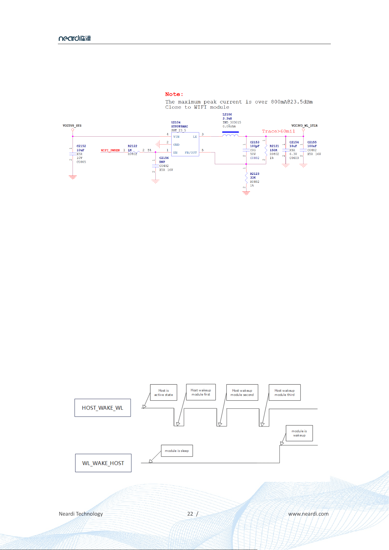
7.1.3 Power Supply Reference
Under different standards, when Wi-Fi transmits continuously, the peak value and amplitude of
FD7621S
Neardi Technology www.neardi.com
22 /
the operating current on the main power supply are as shown in the table below. The 3.3V power
converter must be able to provide 1000mA RMS current and fast transient response (when the
transient current change rate is 80mA/us, the voltage drop is less than 100mV).
For the power on/off sequence of the module, please refer to the requirements in the "4.3 Power
On/Off Sequence" chapter.
7.2 Interface Design Notice
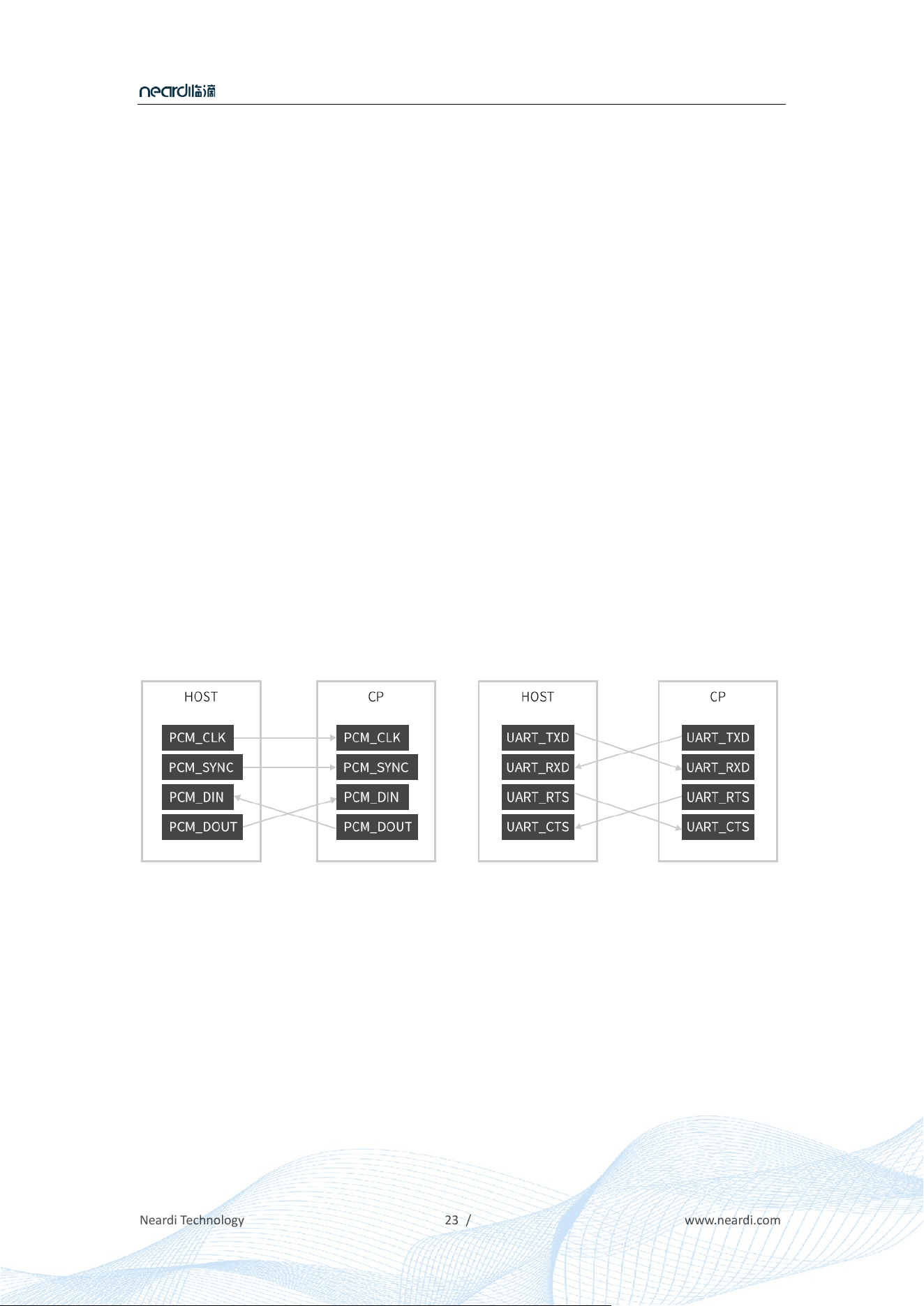
7.2.1 Wake-up Signals
This module require two GPIOs as handshake signals with the host controller, the wake up
direction of these two GPIOs support auto negotiation. As default, for example, WL_ WAKE_
HOST is the output signal "CP wakes up the Host", and HOST_ WAKE_ WL is the input signal "Host
wakes up CP", also we can swap then when connect with the host. Wi-Fi and Bluetooth use the
same handshake signal. The working mechanism is as follows.
FD7621S
Neardi Technology www.neardi.com
23 /
7.2.2 HCI Commend Interface
The Bluetooth supports SDIO3.0 and HS-UART (4Mbps) as HCI (Host Controller Interface).
SDIO3.0 is used as HCI by default, which means the HS-UART port does not need in the HOST
controller.
7.2.3 SDIO Interface
This module supports SDIO3.0. When the input level of VDDIO is 3.3v, SDIO supports the clock
frequencies of 25MHz and 50MHz.When the input level of VDDIO is 1.8v, SDIO supports SDR25,
SDR50 and SDR104, and the clock frequency of SDR104 is 208MHz.
The clock frequency of the SDIO3.0 interface is up to 208MHz. The SDIO bus needs to be
controlled with a single-ended 50 ohm impedance. The maximum length of the bus routing is
15cm. The SDIO signal group needs to be controlled to be of equal length with 100mil.
7.2.4 PCM and UART Interface
As shown in the figure below, the PCM bus and UART bus and data lines between the Host and
the module need to be cross-connected.

FD7621S
Neardi Technology www.neardi.com
24 /
8 Storage,Production and Packaging
8.1 Storage Conditions
FD7621S module is 3 (MSL3) and packed in a vacuum-sealed bag when shipped, the
recommended storage temperature is 25±5°C, and the relative humidity is 35%~60%. Under
this condition, the module can be stored for 12 months.
The Module shall be stored without opening the packing. After the packing opened, the
module shall be completed the patch soldering within 24 hours.
FD7621S module can be stored for no more than 168 hours in a workshop environment with
a temperature of 25±5°C, a relative humidity below 60% and in compliance with IPC/JEDEC
J-STD-033. It is not recommended to expose the module unpacked to the air for a long time.
If not immediately patch soldering, it is recommended to store the module in a
moisture-proof cabinet with a relative humidity of less than 10% to keep the module dry.
If the module is not stored according to the above recommended method, it needs to be
baked at high temperature (120±5°C) for 8 hours. The re-baked module shall be patched
within 24 hours.
Please pay attention to ESD protection when unpacking and handling modules.
8.2 Production Welding
During the production welding process, please do not use any organic solvents (such as alcohol,
isopropanol, acetone, trichloroethylene, etc.) to wipe the shield of the FD7621S module,
otherwise it may cause the shield to rust. Please do not ultrasonically clean the module, it may
cause damage to the crystal inside the module. Please make sure that the spray material used
will not chemically react with the module shield or PCB and will not flow into the module when
spraying modules.
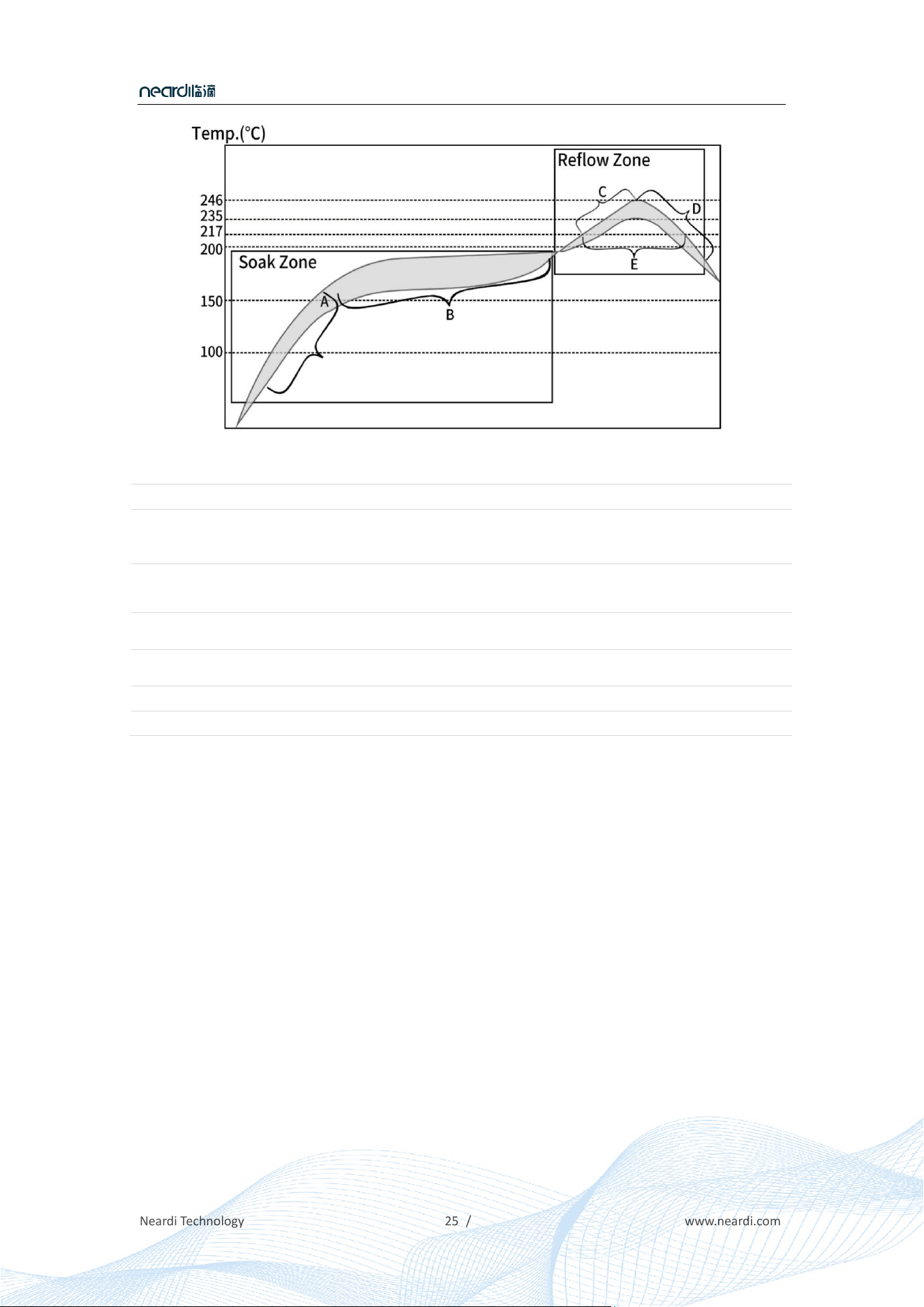
In order to ensure the welding quality and reliability of the FD7621S module, the thickness of the
printed stencil is recommended to be 0.15~0.18mm; the recommended reflow curve is as
follows:
FD7621S
Neardi Technology www.neardi.com
25 /
Recommended reflow curve
Item Description Value
Endothermic Zone Heating Rate Interval A ≤3℃/s
Soak time
From the end of interval A to the beginning of
interval B
60~120s
Reflow Zone Heating Rate Interval C ≤3 ℃/s
Maximum Temperature Highest point of the curve 246℃(+5/-0℃)
Cooling Rate Interval D <6 ℃/s
Reflow Time Interval E 60~150 seconds
8.3 Packing Specifications
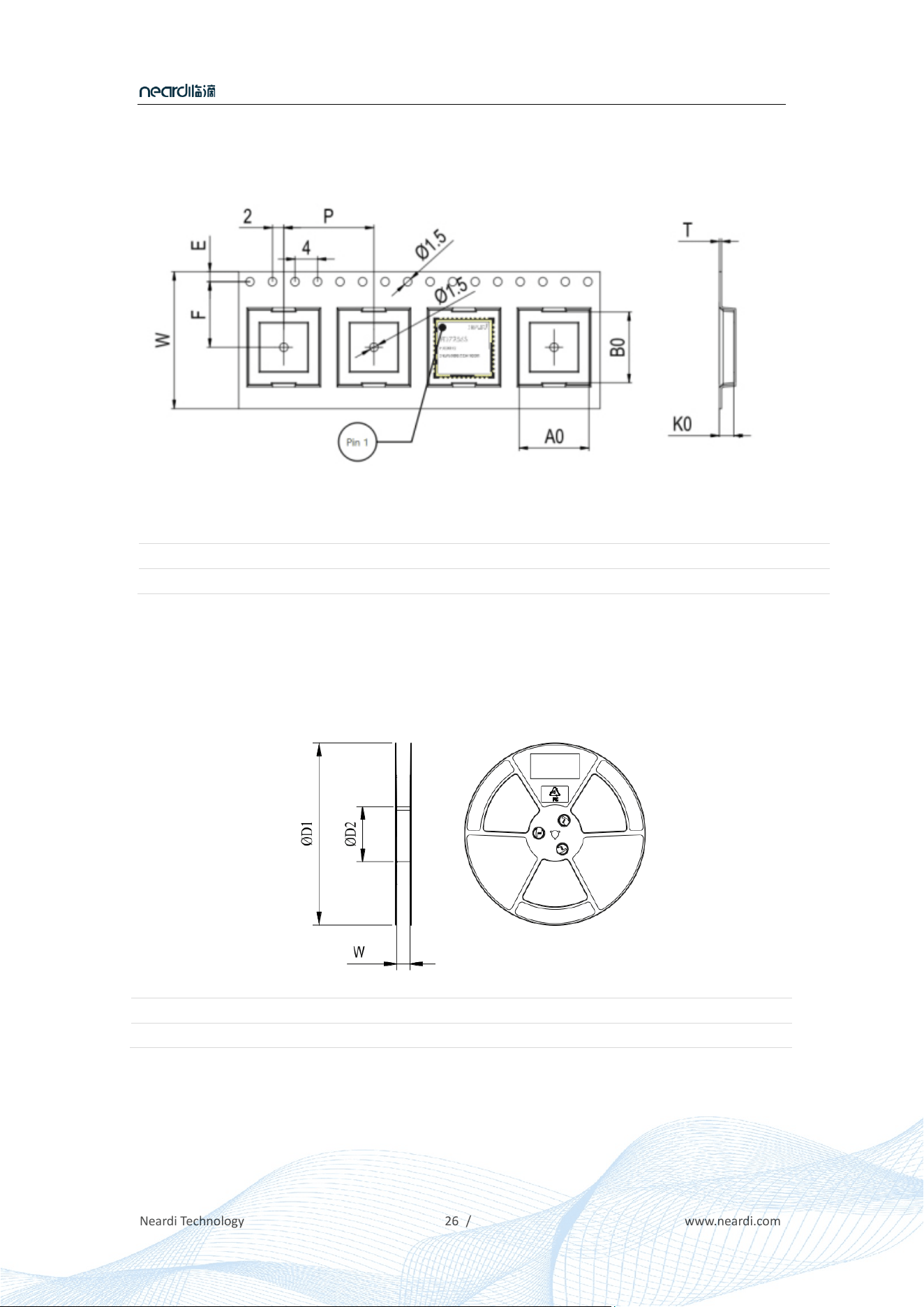
The key parameters and packaging processes described in this chapter are for reference only. The
appearance and structure of the specific packaging materials are subject to actual delivery.
FD7621S
Neardi Technology www.neardi.com
26 /
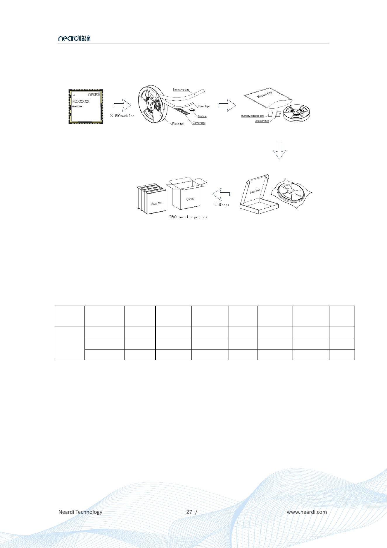
8.3.1 Tape Dimensions
Tape dimensions
W P T A0 B0 K0 F E. Unit
24 16 0.35 12.4 12.4 2.5 11.5 1.75 mm
8.3.2 Plastic Reel Dimensions
ΦD1 φD2 W unit
330 100 24 mm
FD7621S
Neardi Technology www.neardi.com
27 /
8.3.3 Packaging Process
Package specification
8.3.4 Ordering Information
Product Model Marking Data Rate Throughput Antenna Bandwidth Frequency
Band
BT&BLE
FD7621S FD7621S-0 200S31-0 600.5Mbps 520Mbps 1T1R 80M 2.4+5G BT+BLE
FD7621S-1 200S31-1 286.8Mbps 270Mbps 1T1R 40M 2.4+5G BT+BLE
FD7621S-2 200S31-2 286.8Mbps 270Mbps 1T1R 40M 2.4+5G BLE

FD7621S
Neardi Technology www.neardi.com
28
/
9 Antenna Design
9.1 Summarize
This device complies with part 15 of the FCC Rules. Operation is subject to the following two conditions:
(1) This device may not cause harmful interference, and
(2) this device must accept any interference received, including interference that may cause undesired
operation.
This equipment has been tested and found to comply with the limits for a Class B digital device, pursuant to
part 15 of the FCC Rules. These limits are designed to provide reasonable protection against harmful
interference in a residential installation. This equipment generates, uses and can radiate radio frequency
energy and, if not installed and used in accordance with the instructions, may cause harmful interference to
radio communications. However, there is no guarantee that interference will not occur in a particular installation.
If this equipment does cause harmful interference to radio or television reception, which can be determined by
turning the equipment off and on, the user is encouraged to try to correct the interference by one or more of the
following
measures:
- Reorient or relocate the receiving antenna.
- Increase the separation between the equipment and receiver.
- Connect the equipment into an outlet on a circuit different from that to which the receiver is connected.
- Consult the dealer or an experienced radio/TV technician for help.
This modular has been tested and found to comply with part 15 requirements for Modular
Approval.
- FCC Caution: Any changes or modifications not expressly approved by the party responsible for compliance
could void the user's authority to operate the equipment. This transmitter must not be co-located or operating in
conjunction with any other antenna or
transmitter.
- Integration instructions for host product manufacturers according to KDB 996369 D03
OEM Manual v01r01
9.2 List of applicable FCC rules
CFR 47 FCC Part 15 Subpart C and Subpart F has been investigated. It is applicable to the modular transmitter
FD7621S
Neardi Technology www.neardi.com
29
/
9.3 Specific Operational Use Conditions-Antenna Placement Within the Host Platform
The module is tested for standalone mobile RF exposure use condition.
● The antenna must be installed such that 20cm is maintained between the antenna and
users,
● The transmitter module may not be co-located with any other transmitter or antenna.In the event that these
conditions cannot be met (for example certain laptop configurations or co-location with another transmitter),
then the FCC authorization is no longer considered valid and the FCC ID cannot be used on the final product.
In these
circumstances, the OEM integrator will be responsible for re-evaluating the end product (including the
transmitter) and obtaining a separate FCC authorization.
9.4 Limited Module Procedures
Not applicable
9.5 Trace Antenna Designs
Users should connect antennas to half hole pad through copper tube structure or FP types of RF trace and the
trace impedance must be controlled in 50Ω.recommends that the total insertion loss between the antenna pads
and antennas should meet
the following requirements:
Frequency
Loss
2400MHz-2500MHz
<0.6dB
5150MHz-5850MHz
<1.2dB
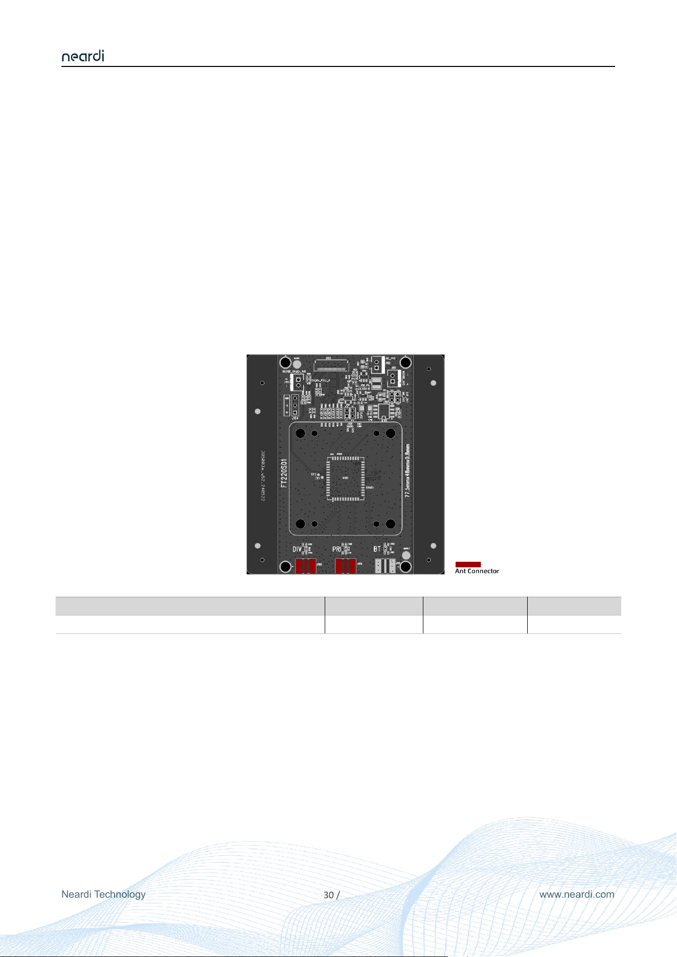
To facilitate the antenna tuning and certification test, a RF connector and an antenna matching circuit should be
added. The following figure is the recommended circuit.
FD7621S
Neardi Technology www.neardi.com
30
/
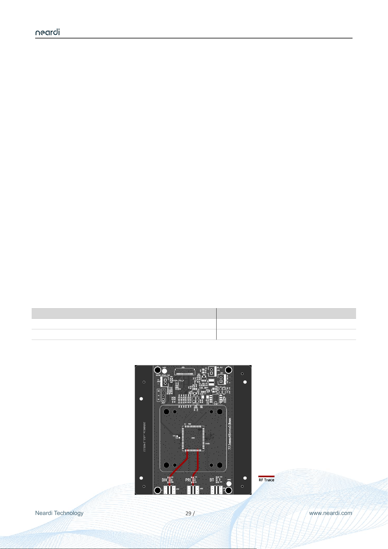
The module needs to be attached to the PCB board and connected to the external antenna
through the solder joint of the circuit on the PCB. The gain of the external antenna is 2dB(i Max.),the internal
structure is copper tube structure or FPC. A resistance of 0R is added between the module and the antenna at
C1003 to ensure that the impedance of the connection between the module and the antenna reaches 50R.The
J0800 position on the PCB is where the external antenna is connected.
RF traces layout
1.Keep the RF trace from module ant pin to antenna as short as possible
2.RF trace should be 50 Ω either on the top layer or in the inner layer
3.RF trace should be avoided right angle and sharp angle.
4.Put enough GND vias around RF traces.
5.RF trace should be far away from other high speed signal lines.
External Antenna VSWR
9.6 RF Exposure Considerations
This device complies with FCC radiation exposure limits set forth for an uncontrolled environment. This
equipment should be installed and operated with minimum distance 20cm between the radiator & your body
9.7 Antenna Type and Gain
The following antennas have been certified for use with this module.
Only antennas of the same type with equal or lower gain may also be used with this module.
Parameters
Min
Typ
Max
External Antenna VSWR
1
1.6
2.0
FD7621S
Neardi Technology www.neardi.com
31
/
Other types of antennas and/or higher gain antennas may require the additional authorization for operation.
Antenna Specification list below:
Model
Type
Connector
Peak gain ( dBi )
2400-2483.5
MHz
5150-5250
MHz
5250-5350
MHz
5470-5725
MHz
5725-5850
MHz
FD7621S
External
Antenna
/
2.00dBi
2.00dBi
2.00dBi
2.00dBi
2.00dBi
9.8 End Product Labelling Compliance Information
When the module is installed in the host device, the FCC ID label must be visible through a window on the final
device or it must be visible when an access panel, door or cover is easily removed. If not, a second label must
be placed on the outside of the final device
that contains the following text: “Contains FCC ID: 2BFAK-FD220S”. The FCC ID can be
used only when all FCC compliance requirements are met
9.9 Information on Test Modes and Additional Testing Requirements
This transmitter is tested in a standalone mobile RF exposure condition and any co-located or simultaneous
transmission with other transmitter(s) class II permissive change re-evaluation or new FCC authorization.
Host manufacturer installed this modular with single modular approval should perform the
test of radiated emission and spurious emission according to FCC part 15C, Part 15E,
15.209, 15.207 requirement, only if the test result comply with FCC part 15C, Part 15E,
15.209, 15.207 requirement, then the host can be sold legally.
9.10 Additional testing, Part 15 Subpart B Disclaimer
This transmitter modular us tested as a subsystem and its certification does not cover the FCC Part 15 Subpart
B rules requirement applicable to the final host. The final host will still need to be reassessed for compliance to
this portion of rules requirements if applicable.
As long as all conditions above are met, further transmitter test will not be required. However, the OEM
integrator is still responsible for testing their end-product for any additional compliance requirements required
with this modular installed.

FD7621S
Neardi Technology www.neardi.com
32
/
8.11 Note EMI Considerations
The OEM integrator has to be aware not to provide information to the end user regarding how to install or
remove this RF module in the user’s manual of the end product which integrates this module.
The host integrator must follow the integration instructions provided in this document and ensure that the
composite system end product complies with the requirements by a technical assessment or evaluation to the
rules and to KDB Publication 996369.
The host integrator installing this module into their product must ensure that the final composite product
complies with the requirements by a technical assessment or evaluation to the rules, including the transmitter
operation and should refer to guidance in KDB Publication 996369.
OEM/Host Manufacturer Responsibilities
OEM/Host manufacturers are ultimately responsible for the compliance of the Host and Module. The final
product must be reassessed against all the essential requirements of the FCC rule such as FCC Part 15
Subpart B before it can be placed on the US market.
This includes reassessing the transmitter module for compliance with the Radio and RF Exposure essential
requirements of the FCC rules.
8.12 How to Make Changes - Important Note
In the event that these conditions cannot be met (for example certain laptop configurations or co-location with
another transmitter), then the FCC authorization is no longer considered valid and the FCC ID cannot be used
on the final product. In these circumstances, the OEM integrator will be responsible for re-evaluating the end
product (including the transmitter) and obtaining a separate FCC authorization.