
User Manual for
TL3228X-DG96D Dongle Board
UM-TL3228X-DG96D-E1
Ver 1.0.0
2026/06/16
Keyword
TL3228X-DG96D, Bluetooth
®
LE, Zigbee, Thread, Matter, 2.4 GHz
Brief
This document is the dongle board user manual for the Telink multi-standard wireless SoC TL3228X. It mainly
introduces the development board diagram, features, peripheral interfaces, and detailed function descriptions.
TL3228X-DG96D Dongle Board User Manual
UM-TL3228X-DG96D-E1 1 Ver 1.0.0
Published by
Telink Semiconductor
10-11/F, Building 1, 61 Shengxia Road,
Pudong District, Shanghai, China 201203
© Telink Semiconductor
All Rights Reserved
Legal Disclaimer
This document is provided as-is. Telink Semiconductor reserves the right to make improvements without
further notice to this document or any products herein. This document may contain technical inaccuracies or
typographical er
rors. Telink Semiconductor disclaims any and all liability for any errors, inaccuracies or
incompleteness contained herein.
Copyright © 2026 Telink Semiconductor (Shanghai) Co., Ltd.
Information
For further information on the technology, product, and business terms, please contact Telink Semiconductor
Company (www.telink-semi.com
).
For sales or technical support, please send an email to the address:
TL3228X-DG96D Dongle Board User Manual
UM-TL3228X-DG96D-E1 2 Ver 1.0.0
Revision History
Version
Change Description
1.0.0 Initial release.
TL3228X-DG96D Dongle Board User Manual
UM-TL3228X-DG96D-E1 3 Ver 1.0.0
Table of Content
1 Overview....................................................................................................................................... 6
1.1 Block Diagram........................................................................................................................ 7
1.2 Board Features ...................................................................................................................... 8
1.3 Kit List.................................................................................................................................. 8
1.4 Board Pictures ....................................................................................................................... 8
1.5 Connectors ...........................................................................................................................10
1.6 LED ..................................................................................................................................... 11
1.7 Button ................................................................................................................................. 12
2 Function Description...................................................................................................................... 13
2.1 Power Supply ....................................................................................................................... 13
2.2 Debug and GPIO Interfaces..................................................................................................... 14
2.3 RF Test................................................................................................................................ 15
2.4 Peripheral Interface - USB Type-A .......................................................................................... 15
2.5 Peripheral Interface - Flash .................................................................................................... 16
3 Related Documents ....................................................................................................................... 17
4 Certification Statement .................................................................................................................. 18
4.1 FCC Statement ..................................................................................................................... 18
TL3228X-DG96D Dongle Board User Manual
UM-TL3228X-DG96D-E1 4 Ver 1.0.0
List of Figures
Figure 1-1 Board Top View ................................................................................................................. 7
Figure 1-2 Board Bottom View............................................................................................................ 7
Figure 1-3 Real Board Top View.......................................................................................................... 9
Figure 1-4 Real Board Bottom View..................................................................................................... 9
Figure 1-5 Board Top Connectors .......................................................................................................10
Figure 1-6 Board Top LEDs ................................................................................................................ 11
Figure 1-7 Board Top Buttons ............................................................................................................ 12
Figure 2-1 Power Supply Path............................................................................................................ 13
Figure 2-2 Debug and GPIO Interfaces on the Board ............................................................................. 15
TL3228X-DG96D Dongle Board User Manual
UM-TL3228X-DG96D-E1 5 Ver 1.0.0
List of Tables
Table 1-1 Board Features .................................................................................................................. 8
Table 1-2 Kit List ............................................................................................................................. 8
Table 1-3 Board Top Connector List................................................................................................... 10
Table 1-4 Board Top LEDs ................................................................................................................ 11
Table 1-5 Board Top Button List ....................................................................................................... 12
Table 2-1 Power Supply of the Chip .................................................................................................. 13
Table 2-2 Debug Methods................................................................................................................ 14
Table 2-3 GPIO Connections............................................................................................................. 14
Table 2-4 RF Test Method................................................................................................................ 15
Table 2-5 DM and DP of USB ........................................................................................................... 16
Table 2-6 Connections of Flash Pins.................................................................................................. 16
Table 3-1 Related Documents........................................................................................................... 17
TL3228X-DG96D Dongle Board User Manual
UM-TL3228X-DG96D-E1 6 Ver 1.0.0
1 Overview
The TL3228X-DG96D dongle board is designed based on the TL3228X chip.
The TL3228X is a wireless SoC for Bluetooth
®
LE 6.0, 802.15.4, and 2.4 GHz proprietary. This chip supports
industrial alliance standards including Bluetooth
®
LE, Zigbee, Thread, Matter, and 2.4 GHz proprietary
standard.
This development board supports testing of various functions, such as RF conduction
testing, lights, and
buttons. Sufficient GPIOs are reserved for debugging.
This document provides a detailed description of the TL3228X-DG96D dongle board's interfaces, power supply,
debugging methods, buttons, LEDs, and other components to help users familiarize themselves with the board
and use it for subsequent development and debugging.
TL3228X-DG96D Dongle Board User Manual
UM-TL3228X-DG96D-E1 7 Ver 1.0.0
1.1 Block Diagram
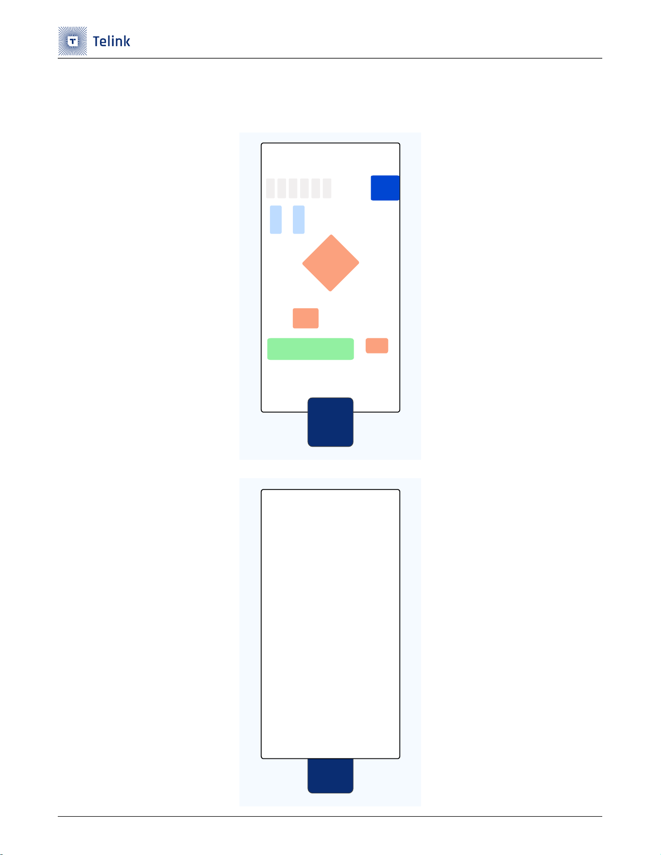
The top and bottom views of the TL3228X-DG96D dongle board are shown below.
Figure 1-1 Board Top View
Figure 1-2 Board Bottom View
USB
Type-A
RF SOC
TL3228X
FLASH
LED
LDO
LED
LED
LED
LED
BUTTON
ANTENNA
LED
2×8 HEADER
BUTTON
SMA
Connector
USB
Type-A
TL3228X-DG96D Dongle Board User Manual
UM-TL3228X-DG96D-E1 8 Ver 1.0.0
1.2 Board Features
The following table lists the features of the TL3228X-DG96D dongle board.
Table 1-1 Board Features
1.3 Kit List
The following table lists the main materials in this development kit.
Table 1-2 Kit List
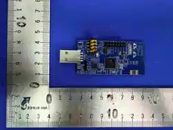
1.4 Board Pictures
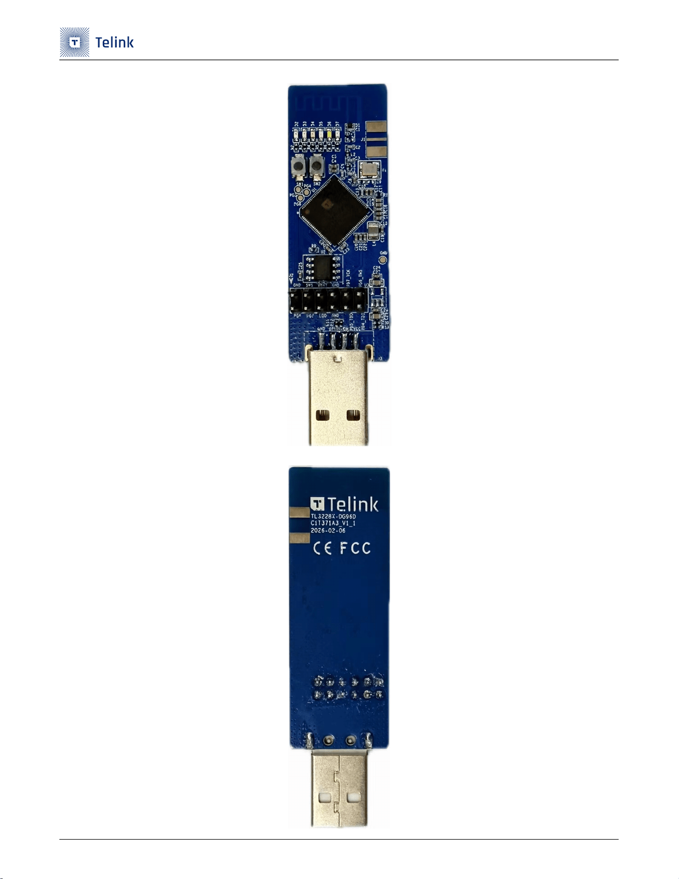
The following picture shows the board's default state for user verification.
No. Name Description Reference section
1
Power supply
interface
Power supply via USB Type-A 2.1 Power Supply
2
Debug and GPIO
interfaces
• Supports 2-wire SDP and 4-wire JTAG
interface
• Supports High-speed USB interface
• 6 GPIOs are reserved for debugging
2.2 Debug and GPIO Interfaces
3 RF interface
• Supports external whip antenna
• Supports onboard inverted-F PCB antenna
2.3 RF Test
4 Peripheral interface
Supports peripherals such as buttons, LEDs, an
external flash.
2.4 Peripheral Interface - USB Type-A
2.5 Peripheral Interface - Flash
No. Name Quantity
1 TL3228X-DG96D dongle board 1
2 Whip antenna 1
3 Display (optional) 1
TL3228X-DG96D Dongle Board User Manual
UM-TL3228X-DG96D-E1 9 Ver 1.0.0
Figure 1-3 Real Board Top View
Figure 1-4 Real Board Bottom View
TL3228X-DG96D Dongle Board User Manual
UM-TL3228X-DG96D-E1 10 Ver 1.0.0
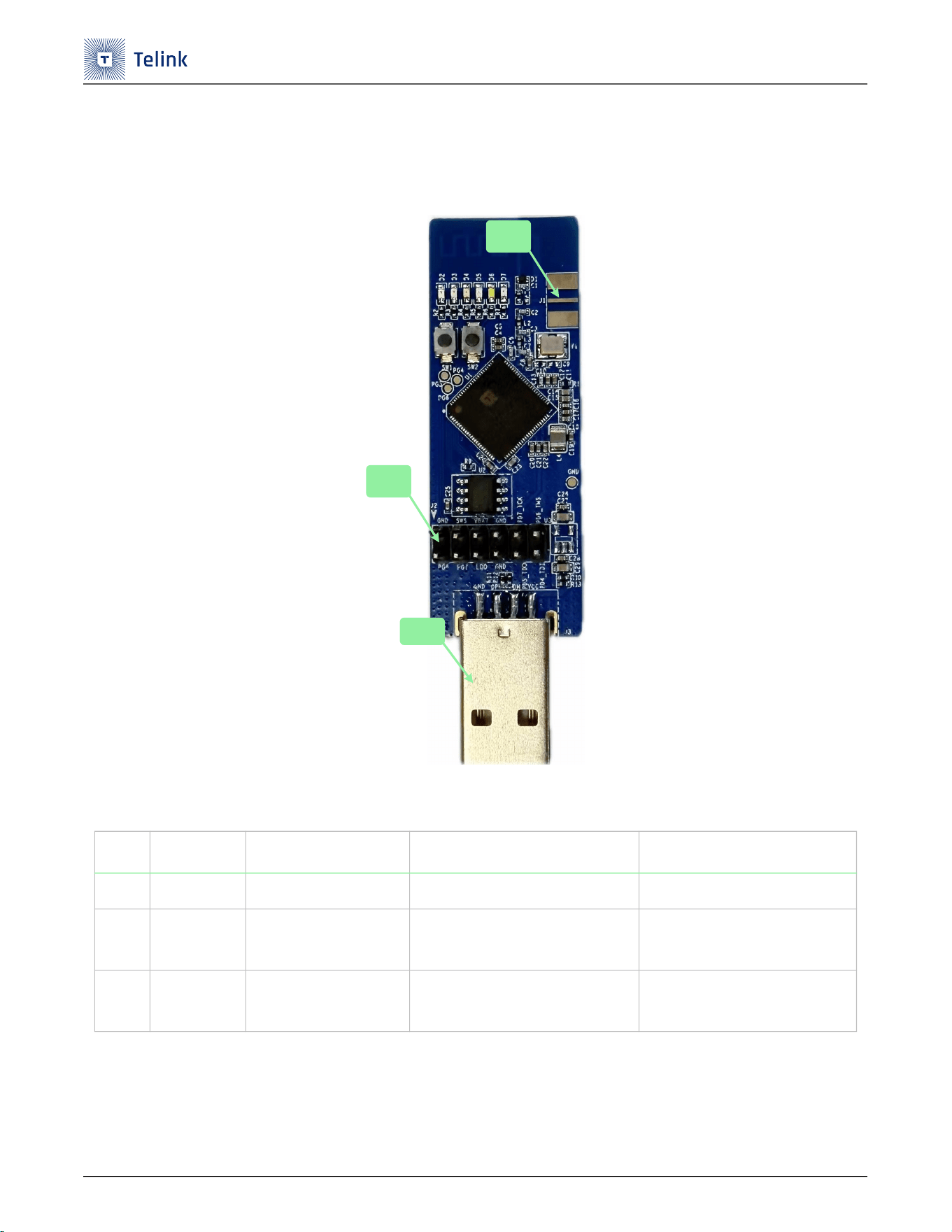
1.5 Connectors
The following figure identifies the connectors such as test headers and sockets on the top of the development
board.
Figure 1-5 Board Top Connectors
The following table lists the connectors on the top of the development board.
Table 1-3 Board Top Connector List
No. Ref. Des. Connector type Description Reference section
1 J1 SMA connector RF connector 2.3 RF Test
2 J2 2x6-pin header
JTAG, single wire, debug and
GPIO connector
2.2 Debug and GPIO Interfaces
3 J3 USB Type-A High-speed USB connector
2.4 Peripheral Interface - USB
Type-A
J2
J3
J1
TL3228X-DG96D Dongle Board User Manual
UM-TL3228X-DG96D-E1 11 Ver 1.0.0
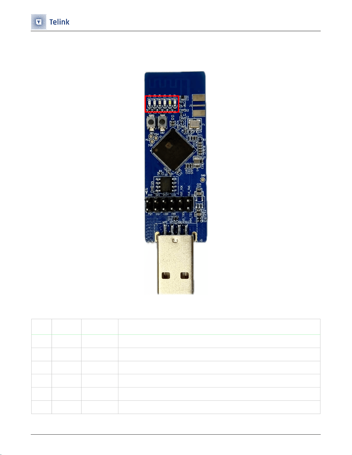
1.6 LED
The following figure identifies the LEDs on the top of the development board.
Figure 1-6 Board Top LEDs
The following table lists the LEDs on the top of the board.
Table 1-4 Board Top LEDs
No. Ref. Des. LED color Description
1 D2 Green PF6 of TL3228X connects to D2 via current-limiting resistor R2.
2 D3 Red PF5 of TL3228X connects to D3 via current-limiting resistor R3.
3 D4 Yellow PF4 of TL3228X connects to D4 via current-limiting resistor R4.
4 D5 Blue PF3 of TL3228X connects to D5 via current-limiting resistor R5.
5 D6 White PF1 of TL3228X connects to D6 via current-limiting resistor R6.
6 D7 Orange PF0 of TL3228X connects to D7 via current-limiting resistor R7.
TL3228X-DG96D Dongle Board User Manual
UM-TL3228X-DG96D-E1 12 Ver 1.0.0
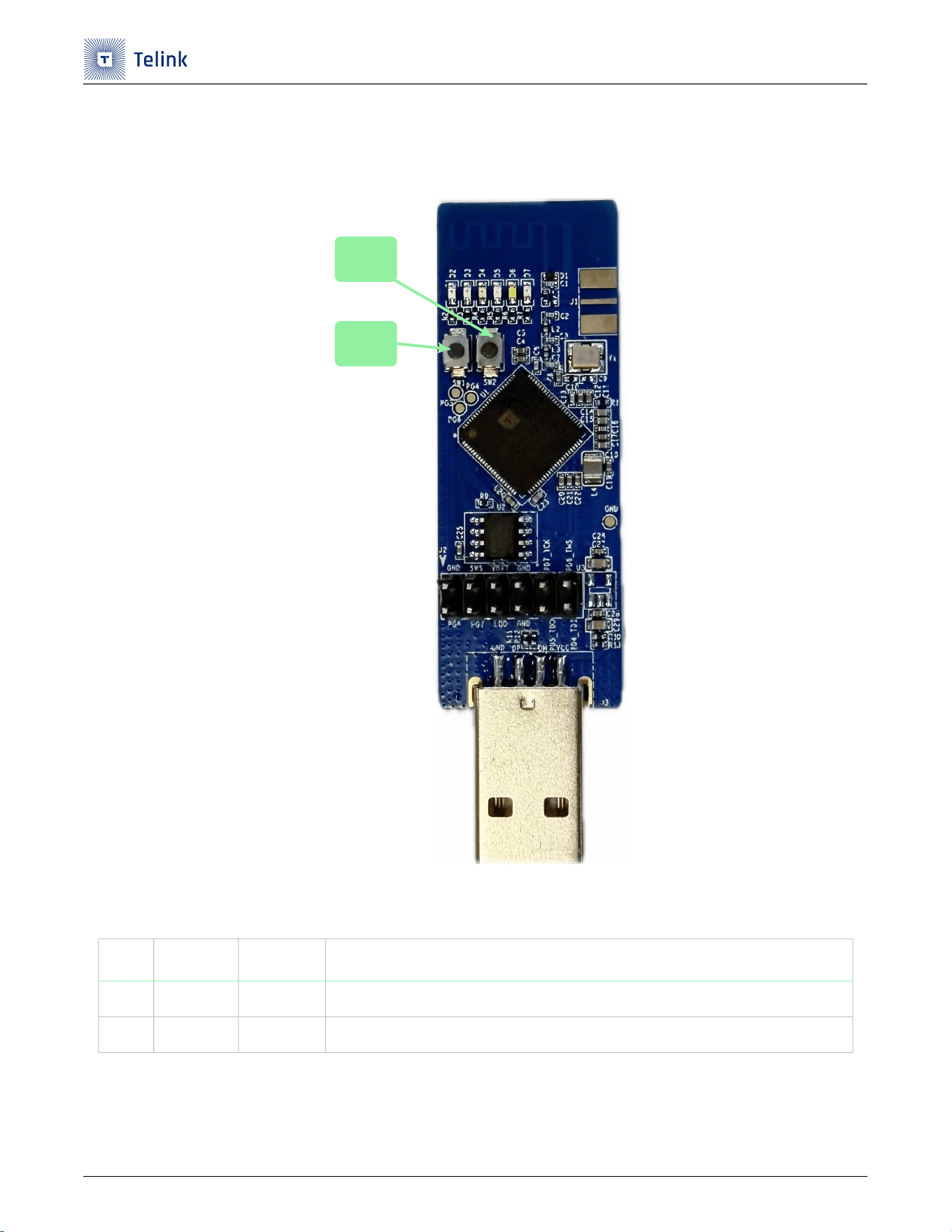
1.7 Button
The following figure identifies the Buttons on the top of the board.
Figure 1-7 Board Top Buttons
The following table lists the buttons on the top of the board.
Table 1-5 Board Top Button List
No. Ref. Des. Function Description
1 SW2 GPIO KEY PF2 of TL3228X connects to SW2.
2 SW1 GPIO KEY PF7 of TL3228X connects to SW1.
SW1
SW2
TL3228X-DG96D Dongle Board User Manual
UM-TL3228X-DG96D-E1 13 Ver 1.0.0
2 Function Description
2.1 Power Supply
The TL3228X-DG96D dongle board can be powered in the following ways:
• 5 V via the USB Type-A port, directly supplying the chip VBUS pin.
The following table shows the chip's power path.
Table 2-1 Power Supply of the Chip
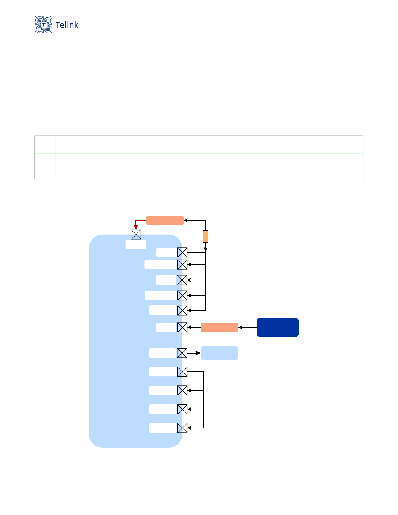
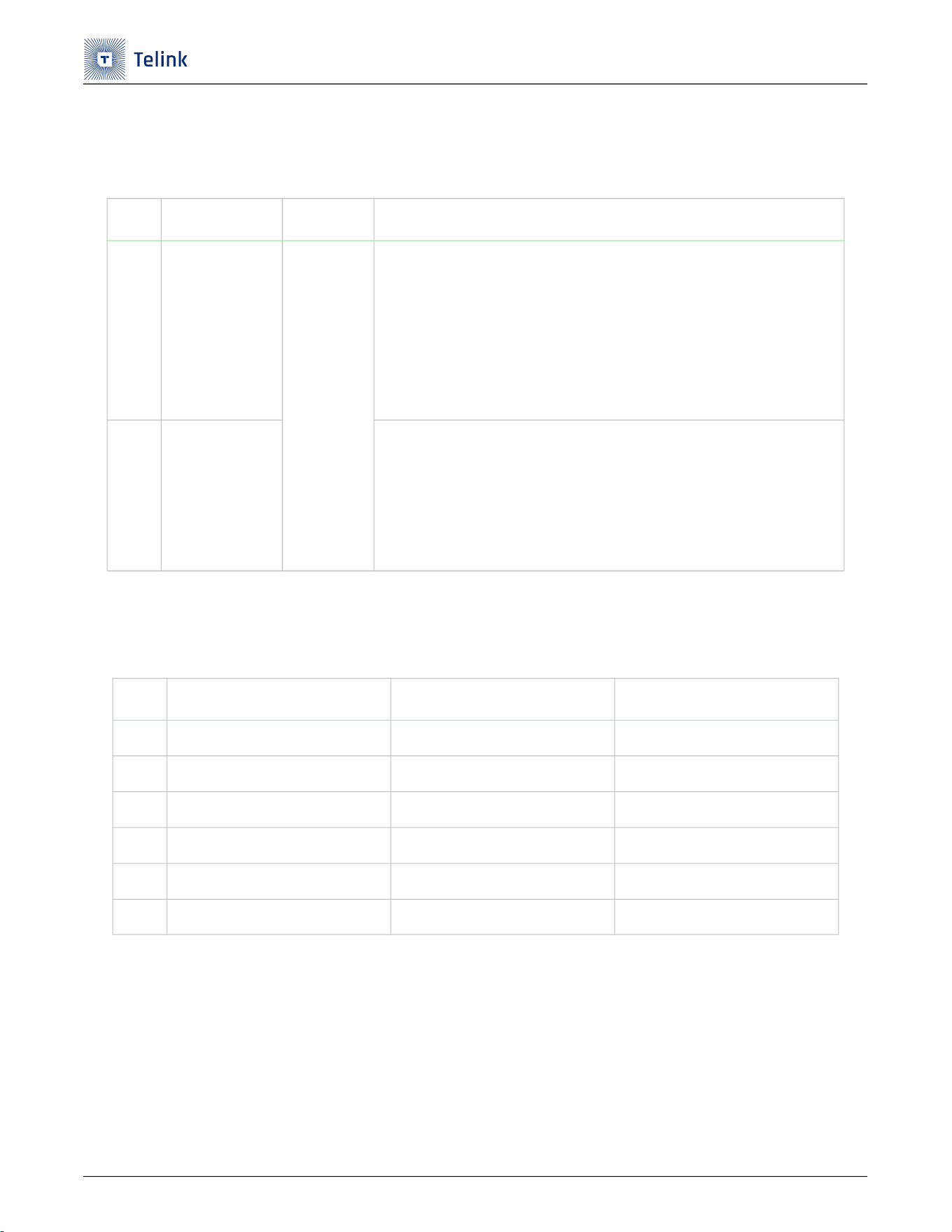
The following figure shows the power supply path of the main power sources.
Figure 2-1 Power Supply Path
No. Power source Power supply Description
1
External power via
USB Type-A J5
5V
Directly supplying the chip VBUS pin. The chip VDDO3 is connected to
VBAT by default through the 0 Ω resistor at R8.
Type-C
High-speed USB
TL_5V
TL3228X
TL_VBAT
J3
U2
VBUS
VBAT
VDDO3
AVDD3
VDDIOAMS
VDD3DCDC
VDDIOF FLASH U5
VDDIOPE
VDD1P2
AVDD1P2
DVDD1P2
VLINE
R8
TL3228X-DG96D Dongle Board User Manual
UM-TL3228X-DG96D-E1 14 Ver 1.0.0
2.2 Debug and GPIO Interfaces
The TL3228X-DG96D dongle board supports the following two debug methods.
Table 2-2 Debug Methods
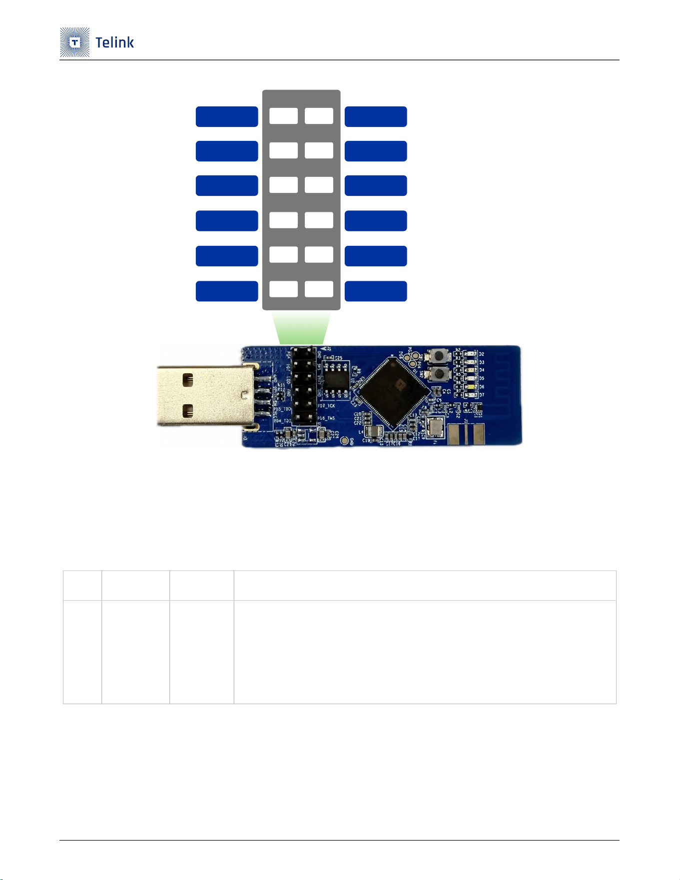
On the TL3228X-DG96D dongle board, some GPIOs are connected to the connectors for easy access.
The following table lists the connections of all GPIOs.
Table 2-3 GPIO Connections
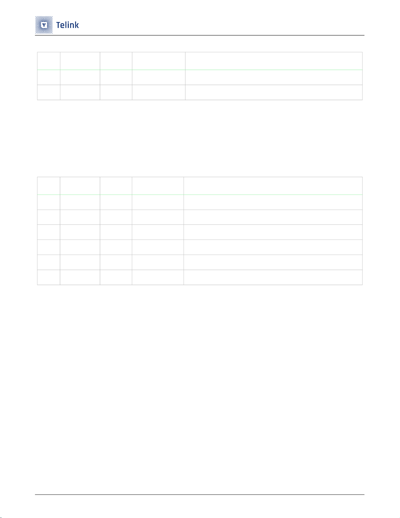
The following figure shows the details of each J2 pin, including the debug and GPIO interfaces.
No. Debug method Connector Description
1 JTAG
J4
(1) Power up the TL3228X-DG96D dongle board.
(2) J2 supports a 4-wire JTAG function
• U1.PIN19.PD4 to J2.PIN12 - TDI
• U1.PIN18.PD5 to J2.PIN10 - TDO
• U1.PIN17.PD6 to J2.PIN11 - TMS
• U1.PIN16.PD7 to J2.PIN09 - TCK
2 Single Wire
(1) Power up the TL3228X-DG96D dongle board.
(2) J2 supports Telink proprietary debug protocol, single wire.
• U1.PIN37.PA7 to J2.PIN03 - SWS
(3) Connect the SWM of the burner with this SWS.
(4) The SWS connects to U1.PIN37 of the chip.
No. Chip pins IO name Connector pins
1 U1.PIN92 PG6 J2.PIN02
2 U1.PIN93 PG7 J2.PIN04
3 U1.PIN16 PD7 J2.PIN09
4 U1.PIN17 PD6 J2.PIN11
5 U1.PIN18 PD5 J2.PIN10
6 U1.PIN19 PD4 J2.PIN12
TL3228X-DG96D Dongle Board User Manual
UM-TL3228X-DG96D-E1 15 Ver 1.0.0
Figure 2-2 Debug and GPIO Interfaces on the Board
2.3 RF Test
The methods for conducting and radiating RF tests on the TL3228X-DG96D dongle board are provided.
The following table lists the methods of RF test.
Table 2-4 RF Test Method
2.4 Peripheral Interface - USB Type-A
The TL3228X-DG96D dongle board is designed with a USB Type-A connector for power supply and high-speed
communication support.
The following table lists the connections of DM and DP.
No. Test item Connector Description
1 RF test J1
(1) Power up the TL3228X-DG96D dongle board normally.
(2) RF radiation test: The on-board PCB antenna is used by default, allowing RF
radiation testing to be performed directly.
(3) RF conduction test: Move the default 0 Ω resistor populated at L1 to R1, then
solder an SMA connector to perform RF conduction testing.
PG6
PG7
LDO
GND
PD5_TDO
PD4_TDI
GND
SWS
VBAT
GND
PD7_TCK
PD6_TMS
PIN02 PIN01
PIN04 PIN03
PIN06 PIN05
PIN08 PIN07
PIN10 PIN09
J2
PIN12 PIN11
TL3228X-DG96D Dongle Board User Manual
UM-TL3228X-DG96D-E1 16 Ver 1.0.0
Table 2-5 DM and DP of USB
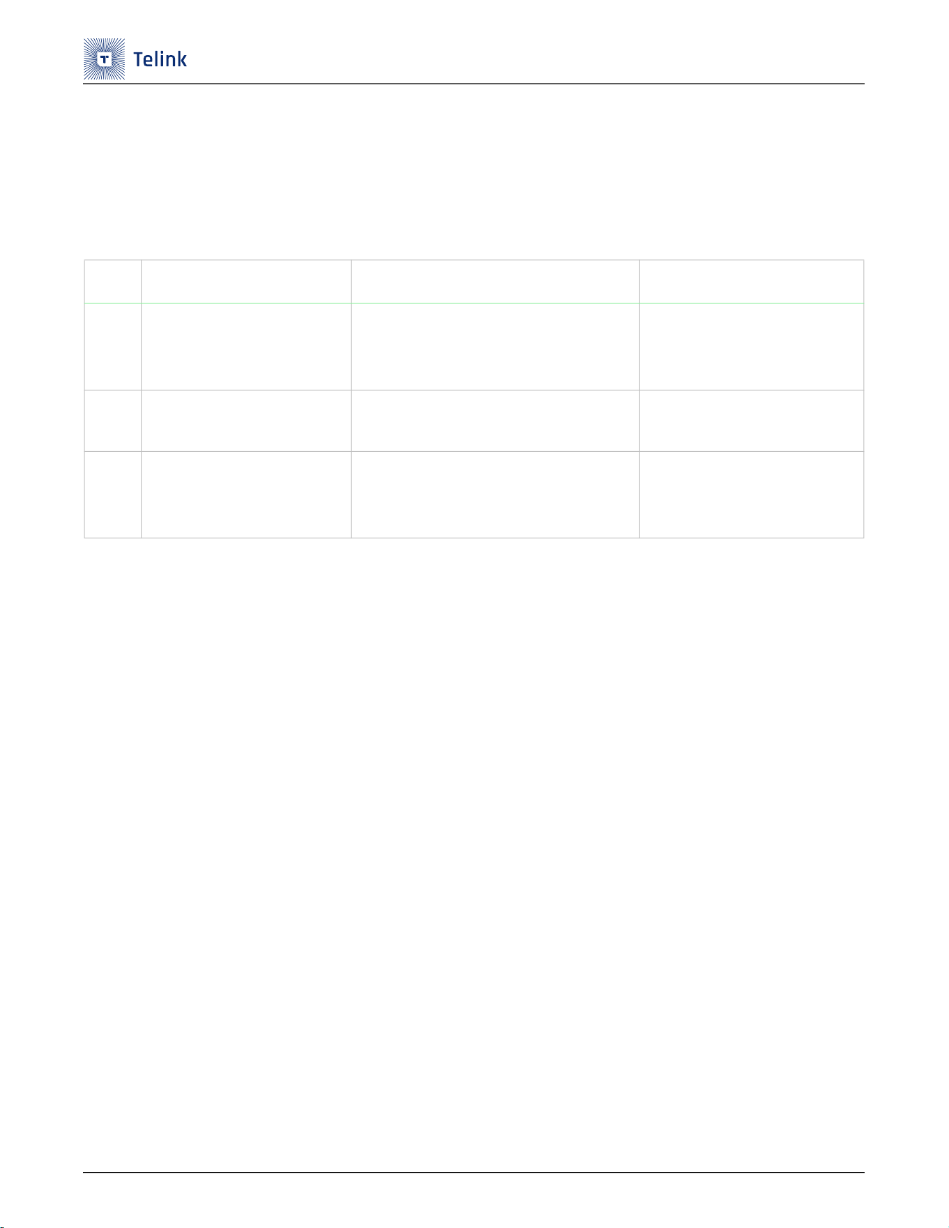
2.5 Peripheral Interface - Flash
The TL3228X-DG96D dongle board is equipped with an external flash (part number P25Q16SU), which makes
it convenient for customers to extend its use or verify the new flash.
The following table lists the connections of the flash pins.
Table 2-6 Connections of Flash Pins
No. Chip pins IO name Connector pins Description
1 U1.PIN34 PA3 J3.PIN02 Connects to the USB DM pin.
2 U1.PIN33 PA4 J3.PIN03 Connects to the USB DP pin.
No. Chip pins IO name Flash Description
1 U1.PIN01 PI0 U2.PIN05 Connects to the flash MSPI_MOSI pin.
2 U1.PIN02 PI1 U2.PIN06 Connects to the flash MSPI_CK pin.
3 U1.PIN03 PI2 U2.PIN07 Connects to the flash MSPI_IO3 pin.
4 U1.PIN04 PI3 U2.PIN01 Connects to the flash MSPI_CN pin.
5 U1.PIN05 PI4 U2.PIN02 Connects to the flash MSPI_MISO pin.
6 U1.PIN06 PI5 U2.PIN03 Connects to the flash MSPI_IO2 pin.
TL3228X-DG96D Dongle Board User Manual
UM-TL3228X-DG96D-E1 17 Ver 1.0.0
3 Related Documents
The following table lists other documents and resources that you can refer to for more information. Some of
these documents are only available under a Non-Disclosure Agreement (NDA). To access these documents,
please contact your local Telink Field Application Engineer (FAE) or sales representative.
Table 3-1 Related Documents
No. Name Description Link / Obtain method
1 TL3228X datasheet
Provides information on the electrical
characteristics, hardware description, and
ordering options for the TL3228X chip.
Contact a Telink FAE / Sales
representative.
2 TL3228X hardware guideline
Provides a hardware design guide for the
TL3228X chip.
Contact a Telink FAE / Sales
representative.
3
TL3228X-DG96D dongle
board files
Provides design files for the schematic,
PCB layout, and Gerber files for the
TL3228X-DG96D dongle board.
Contact a Telink FAE / Sales
representative.
TL3228X-DG96D Dongle Board User Manual
UM-TL3228X-DG96D-E1 18 Ver 1.0.0
4 Certification Statement
4.1 FCC Statement
This device complies with Part 15 of the FCC rules. Operation is subject to the following two conditions: (1)
this device may not cause harmful interference, and (2) this device must accept any interference received,
including interference that may cause undesired operation.
This equipment has been tested and found to comply with the limits for a Class B digital device, pursuant to
Part 15 of the FCC rules. These limits are designed to provide reasonable protection against harmful
interference in a residential installation. This equipment generates, uses, and can radiate radio frequency
energy and, if not installed and used in accordance with the instructions, may cause harmful interference to
radio communications. However, there is no guarantee that interference will not occur in a particular
installation. If this equipment does cause harmful interference to radio or television reception, which can be
determined by turning the equipment off and on, the user is encouraged to try to correct the interference by
one or more of the following measures:
• Reorient the receiving antenna.
• Increase the separation between the equipment and receiver.
• Connect the equipment into an outlet on a circuit different from that to which the receiver is
connected.
• Consult the dealer or an experienced radio/TV technician for help.
Changes or modifications not expressly approved by the party responsible for compliance could void your
authority to operate the equipment.
RF warning statement:
The device has been evaluated to meet general RF exposure requirement. The device can be used in portable
exposure condition without restriction.
The EUT is for indoor use only.