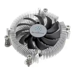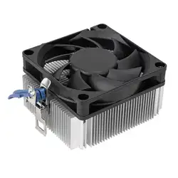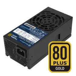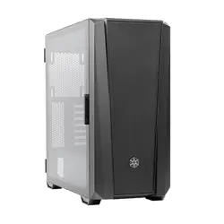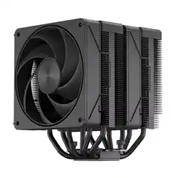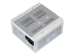

SST-ST40NF
Optimum fan-less power supply
with stability and silence
NIGHTJAR SERIES
SilverStone Nightjar ST40NF
ATX12V 2.3 Switching Power Supply
With Active PFC
PS/2 400W
This is the specification of Model SST-ST40NF; AC-line powered switching power supply
with active PFC (Power Factor Correction) circuit, meet EN61000-3-2 and with AC
Input features 99Vac~264Vac.
The subject power supply will meet the EMI requirements and obtain main safety approvals
as following:
- FCC Part 15 Subpart J, Class ‘B’ 115 Vac operation.
- CISPR 22 Class ‘B’ 230 Vac operation.
NEMKO EN 60950-1
- VDE EN 60950-1
- UL 60950-1
- CB EN 60950-1
IEC 60950-1
- CE :
EN 55022:1998+A1: 2000, Class B
EN 61000-3-2: 2000
EN 61000-3-3: 1995+A1: 2001
CISPR22: 1997+A1: 2000, Class B
AS/NZS CISPR 22: 2002, Class B
2.1 REFERENCE DOCUMENTS
2.2 SAFETY
GENERAL DESCRIPTION AND SCOPE
GENERAL DESCRIPTION AND SCOPE
REFERENCE DOCUMENTS
REFERENCE DOCUMENTS
3. INPUT ELECTRICAL SPECIFICATIONS
4. ELECTRICAL REQUIREMENTS
EN 55024: 1998+A1: 2001
IEC 61000-4-2: 2001
IEC 61000-4-3: 2002
IEC 61000-4-4:1995
+A1:2000+A2: 2001
IEC 61000-4-5: 2001
IEC 61000-4-6: 2001
IEC 61000-4-8: 2001
IEC 61000-4-11: 2001
The +3.3V and +5V total output shall not exceed 130watts, total output power max shall
not exceed 400W ,
Ripple and noise measurements shall be made under all specified load conditions
through a single pole low pass filter with 20MHz cutoff frequency. Outputs shall bypassed
at the connector with a 0.1uF ceramic disk capacitor and a 10uF electrolytic capacitor to
simulate system loading.
The subject power supply will meet all electrical specifications below, over the full operation
temperature range and dynamic load regulation.
4.1.1. OUTPUT RATING
3.1 AC INPUT
3.2 INRUSH CURRENT
4.1 OUTPUT ELECTRICAL REQUIREMENTS
3.3 INPUT LINE CURRENT
(Cold start – 25 deg. C)
SST-ST40NF
GENERAL DESCRIPTION AND SCOPE
REFERENCE DOCUMENTS
3. INPUT ELECTRICAL SPECIFICATIONS
3. INPUT ELECTRICAL SPECIFICATIONS
4. ELECTRICAL REQUIREMENTS
4. ELECTRICAL REQUIREMENTS
Parameter
Min. Max. Unit
Vin Voltage
Vin Frequency
99
47 Hz
264
63
VAC
rms
Hz
115V
230V
No damage
No damage
115V
230V
5.0 Amps – rms maximum
2.5 Amps – rms maximum
Output Nominal Regulation Ripple/Noise Min Max Peak
1
2
3
4
5
+3.3V
+5V
+12V
-12V
+5VSB
±3%
±3%
±3%
±10%
±5%
50mV
50mV
120mV
120mV
50mV
0A
0A
0.2A
0 A
0 A
20.0 A
14.0 A
27.0 A
0.5 A
2.5A
-
-
31.5A
-
3.5A
02
4.2 EFFICIENCY
4.2.1 HOLD-UP TIME (@FULL LOAD)
4.2.2 OUTPUT RISE TIM
4.2.4 SHORT CIRCUIT PROTECTION
Efficiency
In Standby mode, +5Vsb efficiency should be greater than 50% with a minimum loading of
100mA under I/P 230Vac.
99V ~264V: 17 mSec. Minimum.
The output voltage will remain within specification, in the event that the input power is
removed or interrupted, for the duration of one cycle of the input frequency. The interruption
may occur at any point in the AC voltage cycle. The power good signal shall remain high
during this test.
For all output range voltages shall rise from 10% of nominal to within the regulation ranges
specified in Section 4.1.1 within 0.1 ms to 20 ms (0.1 ms T1 20 ms).
(10% TO 90% OF FINAL OUTPUT VALUE, @FULL LOAD)
Output short circuit is defined to be a short circuit load of less than 0.1 ohm.
In the event of an output short circuit condition on +3.3V, +5V, -12V or +12V, the power supply
will shutdown and latch off without damage to the power supply. The power supply shall
return to normal operation after the short circuit has been removed and the power switch has
been turned off for no more than 2 seconds.
Loading Voltage Full load Typical load Light load
Required Minimum Efficiency
115V >82% >85% >82%
Voltage Source
+3.3V
+5V
+12V
3.7V-4.5V
5.7V-7.0V
13.1-15.6V
Protection Point
=
<
=
<
=
<
4.2.3 OVER VOLTAGE PROTECTION
03
SST-ST40NF
4.2.5 OVERLOAD PROTECTION
4.2.6 POWER GOOD SIGNAL
The power good signal is a TTL compatible signal for the purpose of initiating an orderly
star-up procedure under normal input operating conditions. This signal is asserted (low)
until +5Vdc has reached 4.75 volts during power up. Characteristics:
TTTL signal asserted (low state) : less than 0.4V while sinking 4mA.
TTL signal asserted (high state): Between 2.4 V and 5 V output while sourcing 200 µA
High state output impedance: less or equal to 1Kohm from output to common.
OUTPUT VOLTAGE
+3.3V
+5V
+12V
50A
48A
40A
Max. overcurrent limit
POWER GOOD @ 99Vac~264Vac,FULL LOAD
POWER FAIL @99Vac~264Vac, FULL LOAD
100 –500mSec.
1 mSec. minimum
PS_ON ON
OFF
T1 20mS
T2 100~500mS
T3 1mS
+3.3VO/P
+5V O/P
+12VO/P
P. G .
P.G. SENSE
LEVEL 95%
T1 T2 T3
=
=
<
=
<
04
05
4.3 OUTPUT TRANSIENT LOAD RESPONSE
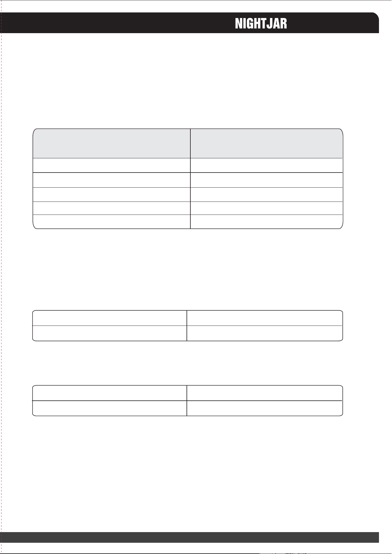
4.4. PS_ ON#
DC Output Transient Step Sizes
summarizes the expected output transient step sizes for each output. The
transient load slew rate is = 1.0 A/μs.
PS_ON# is an active-low, TTL-compatible signal that allows a motherboard to remotely
control the power supply in conjunction with features such as soft on/off, Wake on LAN+,
or wake-on-modem.When PS_ON# is pulled to TTL low, the power supply should turn on
the five main DC output rails: +12VDC,+5VDC,+3.3VDC,and –12VDC. When PS_ON# is
pulled to TTL high or open-circuited, the DC output rails should not deliver current and
should be held at zero potential with respect to ground. PS_ON# has no effect on the
+5VSB output, which is always enabled whenever the AC power is present. Table lists
PS_ON# signal characteristics. The power supply shall provide an internal pull-up to TTL
high. The power supply shall also provide debounce circuitry on PS_ON# to prevent it from
oscillating on/off at startup when activated by a mechanical switch. The DC output enable
circuitry must be SELV-compliant.
Load-changing repetition rate of 50 Hz to 10 kHz
Ac input range per section 3.1
Capacitive loading per section 4.5
Output Max . step size
(amps)
Max. setp size
(% of rated output amps per Sec 4.1.1)
+12VDC
+5VDC
+3.3VDC
-12VDC
+5VSB
50%
30%
30%
-
-
-
-
-
0.1A
0.5A
PS_ON# Signal Characteristics
Min. Max.
VIL, Input Low Voltage
IIL, Input Low Current (Vin = 0.4V)
VIH, Input High Voltage (lin = -200μA)
VIH OPEN circuit, lin = 0
0.0V
-
2.0V
-
0.8V
-1.6mA
-
5.25V
5. ENVIRONMENTAL REQUIREMENTS
SST-ST40NF
06
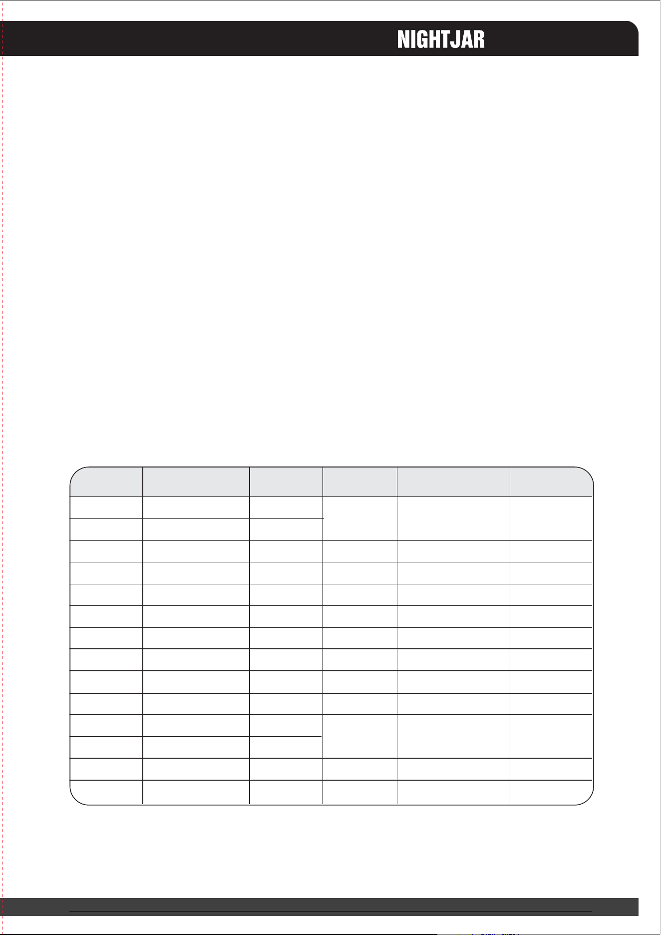
4.5 Capacitive Load
5.1. TEMPERATURE RANGE
5.2 HUMIDITY
Output Capacitive Loads
The power supply should be able to power up and operate normally with the following
capacitances simultaneously present on the DC outputs. This capacitive loading should be
used to check stability and should not be included for noise testing.
The power supply will be compliant with each item in this specification for the following
Environmental conditions.
Output ATX12V
Capacitive load (μF)
+12VDC
+5VDC
+3.3VDC
-12VDC
+5VSB
5000
6000
6000
350
350
5. ENVIRONMENTAL REQUIREMENTS
5. ENVIRONMENTAL REQUIREMENTS
Operating
Storage
0 to 40C
-20 to 80C
O
O
Operating
Storage
5 –95% RH, Non-condensing
5 –95% RH, Non-condensing

07
5.3 VIBRATION
5.4 MECHANICAL SHOCK
6.1 LEAKAGE CURRENT
7.1 LINE CONDUCTED EMI
7.2 RADIATED EMI
The leakage current from AC to safety ground will not exceed 3.5 mA-rms at 264Vac, 50 Hz.
The subject power supply will meet FCC and VFG class B requirements under full load
conditions.
The subject power supply will meet FCC and CISPR 22 requirements under normal load
conditions.
The subject power supply will withstand the following imposed conditions without experiencing
non-recoverable failure or deviation from specified output characteristics.
Vibration Operating – Sine wave excited, 0.25 G maximum acceleration, 10-250 Hz swept at one
octave / min. Fifteen minute dwell at all resonant points, where resonance is defined as those
exciting frequencies at which the device under test experiences excursions two times large than
non-resonant excursions.
Plane of vibration to be along three mutually perpendicular axes.
Non-operating 50 g, trapezoidal input; velocity change 170 in/s
Three drops on each of six faces are applied to each sample.
=
<
6. SAFETY
6. SAFETY
8. LABELLING
9.PHYSICAL REQUIREMENTS
7. ELECTORMAGNETIC COMPATIBILITY
7. ELECTORMAGNETIC COMPATIBILITY
SST-ST40NF
08
8.1 MODEL NUMBER LABEL
Label marking will be permanent, legible and complied with all agency requirements.
150 mm (W) × 86 mm (H) × 160mm (D)
9.1 Physical Dimension
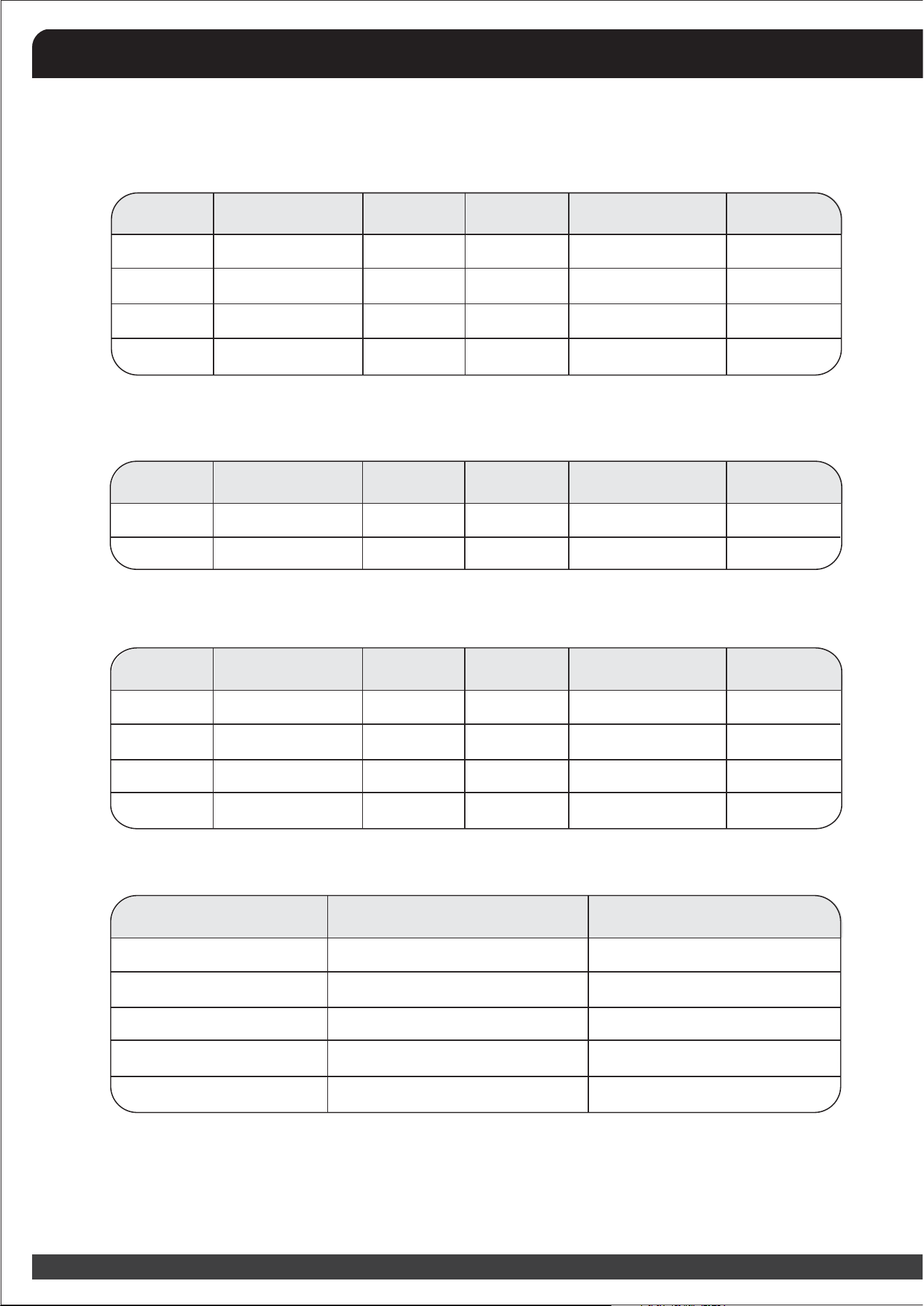
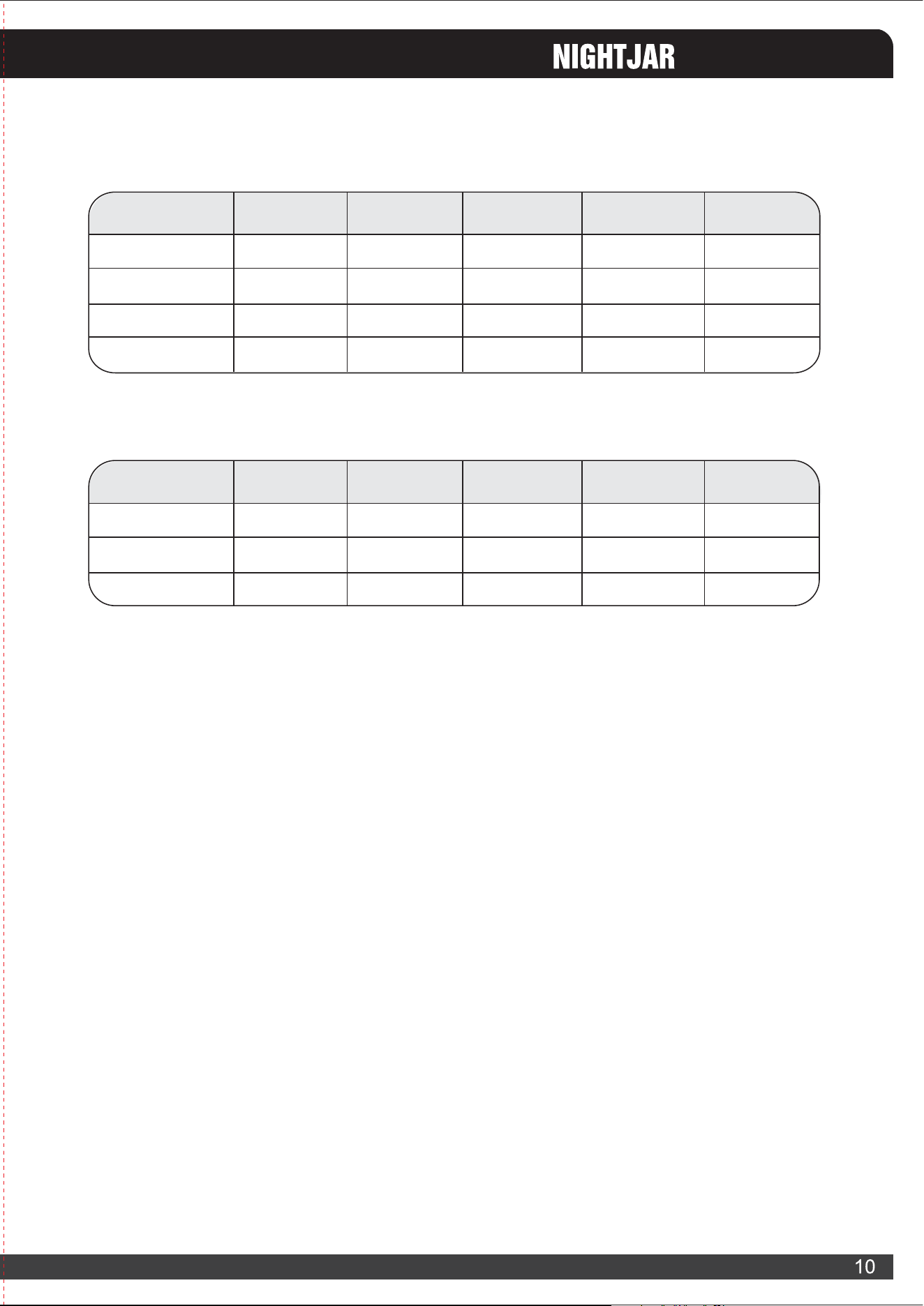
9.2 Connectors Define
Labels will be affixed to the sides of the power supply showing the following:
- Manufacturer’s name and logo.
- Model no., serial no., revision level, location of manufacturer.
- The total power output and the maximum load for each output.
- AC input rating.
6. SAFETY
8. LABELLING
8. LABELLING
9.PHYSICAL REQUIREMENTS
9.PHYSICAL REQUIREMENTS
7. ELECTORMAGNETIC COMPATIBILITY
Signal SignalPin Pin
Orange
Orange
Blue
Black
Green
Black
Black
Black
White
Red
Red
Red
Red
Black
+3.3V
+3.3Vsense
-12VDC
COM
PS-ON
COM
COM
COM
N/C
+5VDC
+5VDC
+5Vsense
+5VDC
COM
13
13
14
15
16
17
18
19
20
21
22
22
23
24
2
3
4
5
6
7
8
9
11
12
+3.3V
COM
+5VDC
COM
+5VDC
COM
PWRGOOD
+5Vsb
+12V
+3.3V
Orange
Black
Red
Black
Red
Black
Grey
Purple
Yellow
Orange
1
10
+12V
+3.3V Orange
Yellow
M/B 24PIN connector
Signal SignalPin Pin
Black
Black
GND
GND
+12V
+12V
Yellow
Yellow
1
2
3
4
ATX 12V 4PIN (4+4PIN EPS 12V in split mode)
Signal SignalPin Pin
Yellow
Black
Black
Red
+12V
COM
COM
+5VDC
+5VDC
COM
COM
+12V
Red
Black
Black
Yellow
1
2
3
4
1
2
3
4
4PIN floppy connector (FDD)4PIN peripheral connector (HDD)
PinSignal
Orange
Black
Red
Black
Yellow
5
4
3
2
1
+3.3V
COM
+5V
COM
+12V
SATA connector
Signal SignalPin Pin
Yellow
Yellow
Yellow
Yellow
+12V
+12V
+12V
+12V
COM
COM
COM
COM
Black
Black
Black
Black
5
6
7
8
1
2
3
4
EPS 12V 8PIN connector
09
SST-ST40NF
Signal SignalPin Pin
Yellow
Yellow
Yellow
Black sense1
+12V
+12V
+12V
COM
COM
COM
COM
COM
Black
Black
Black
Black
1
2
3
4
5
6
7
8
8PIN PCI Express connector
Signal SignalPin Pin
Yellow
Yellow
Yellow
+12V
+12V
+12V
COM
COM
COM
Black
Black
Black
1
2
3
4
5
6
6PIN PCI Express connector
February, 2009
NO:G1120