CD-BK110V/CD-BP99V
No. S0174CDBK110V
CONTENTS
Page
SAFETY PRECAUTION FOR SERVICE MANUAL ........................................................................................................... 2
VOLTAGE SELECTION (CD-BK110V ONLY) ................................................................................................................... 2
AC POWER SUPPLY CORD AND AC PLUG ADAPTOR ................................................................................................. 2
SPECIFICATIONS ............................................................................................................................................................. 3
NAMES OF PARTS ........................................................................................................................................................... 4
OPERATION MANUAL ...................................................................................................................................................... 7
DISASSEMBLY ................................................................................................................................................................ 10
REMOVING AND REINSTALLING THE MAIN PARTS ................................................................................................... 13
ADJUSTMENT ................................................................................................................................................................. 14
NOTES ON SCHEMATIC DIAGRAM .............................................................................................................................. 16
TYPES OF TRANSISTOR AND LED............................................................................................................................... 16
BLOCK DIAGRAM ........................................................................................................................................................... 17
SCHEMATIC DIAGRAM / WIRING SIDE OF P.W.BOARD ..............................................................................................20
VOLTAGE ........................................................................................................................................................................ 43
WAVEFORMS OF CD CIRCUIT ...................................................................................................................................... 44
TROUBLESHOOTING ..................................................................................................................................................... 45
FUNCTION TABLE OF IC................................................................................................................................................ 49
FL DISPLAY ..................................................................................................................................................................... 60
REPLACEMENT PARTS LIST/EXPLODED VIEW
• In the interests of user-safety the set should be restored to its
original condition and only parts identical to those specified be
used.
SERVICE MANUAL
This document has been published to be used
for after sales service only.
The contents are subject to change without notice.
SHARP CORPORATION
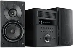
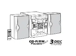
VIDEO CD MINI SYSTEM
MODEL CD-BK110V
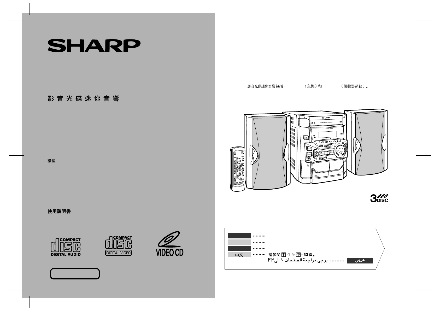
CD-BK110V Video CD Mini System consisting of
CD-BK110V (main unit) and CP-BK110 (speaker system).
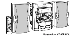
Illustration: CD-BK110V
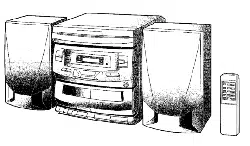
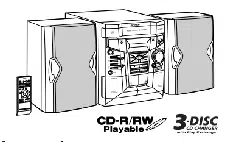
VIDEO CD MINI SYSTEM
MODEL CD-BP99V
CD-BP99V Video CD Mini System consisting of
CD-BP99V (main unit) and CP-BP99 (speaker system).
NTSC/PAL
Illustration: CD-BP99V

CD-BK110V/CD-BP99V
– 2 –
SAFETY PRECAUTION FOR SERVICE MANUAL
WARNINGS
THE AEL (ACCESSIBLE EMISSION LEVEL) OF THE LASER POWER OUTPUT IS LESS THAN CLASS 1 BUT THE LASER
COMPONENT IS CAPABLE OF EMITTING RADIATION EXCEEDING THE LIMIT FOR CLASS 1. THEREFORE IT IS
IMPORTANT THAT THE FOLLOWING PRECAUTIONS ARE OBSERVED DURING SERVICING TO PROTECT YOUR EYES
AGAINST EXPOSURE TO THE LASER BEAM.
1-WHEN THE CABINET IS REMOVED, THE POWER IS TURNED ON WITHOUT A COMPACT DISC IN POSITION AND THE
PICKUP IS ON THE OUTER EDGE THE LASER WILL LIGHT FOR SEVERAL SECONDS TO DETECT A DISC. DO NOT
LOOK INTO THE PICKUP LENS.
2-THE LASER POWER OUTPUT OF THE PICKUP UNIT AND REPLACEMENT SERVICE PARTS ARE ALL FACTORY
PRESET BEFORE SHIPMENT.
DO NOT ATTEMPT TO READJUST THE LASER PICKUP UNIT DURING REPLACEMENT OR SERVICING.
3-UNDER NO CIRCUMSTANCES STARE INTO THE PICKUP LENS AT ANY TIME.
4-CAUTION-USE OF CONTROLS OR ADJUSTMENTS, OR PERFORMANCE OF PROCEDURES OTHER THAN THOSE
SPECIFIED HEREIN MAY RESULT IN HAZARDOUS RADIATION EXPOSURE.
Laser Diode Properties
Material: GaAIAs
Wavelength: 780 nm
Emission Duration: continuous
Laser Output: max. 0.6 mW
Laser Diode Properties
Material: GaAIAs
Wavelength: 780 nm
Emission Duration: continuous
Laser Output: max. 0.6 mW
CAUTION-INVISIBLE LASER RADIATION WHEN OPEN.
DO NOT STARE INTO BEAM OR VIEW DIRECTLY WITH
OPTICAL INSTRUMENTS.
WARNUNG-UNSICHTBARE LASERSTRAHLUNG WENN GERÄT
GEÖFFNET. NICHT IN DIE STRAHLUNG SCHAUEN ODER
DIREKT MIT OPTISCHEN HILFSMITTELN BETRACHTEN.
ATTENTION-RAYON LASER INVISIBLE EN CAS D’OUVERTURE.
NE PAS REGARDER LE FAISCEAU DIRECTEMENT OU AVEC DES
INSTRUMENTS OPTIQUES.
VOLTAGE SELECTION (CD-BK110V ONLY)
AC POWER SUPPLY CORD AND AC PLUG ADAPTOR
Before operating the unit on mains, check the preset voltage. If the voltage is different from your local voltage, adjust the voltage
as follows.
Turn the selector with a screwdriver until the appropriate voltage number appears in the window (110 V, 127 V, 220 V or 230 V-240 V AC).
QACCB0012AW00
QACCE0007AW00
92L24801800222
QPLGA0004AWZZ QPLGA0003AWZZ
For CD-BK110V
For CD-BP99V

– 3 –
CD-BK110V/CD-BP99V
FOR A COMPLETE DESCRIPTION OF THE OPERATION OF THIS UNIT, PLEASE REFER
TO THE OPERATION MANUAL.
Specifications for this model are subject to change without
prior notice.
SPECIFICATIONS
■ General
■ Amplifier
■ CD player
■ Tuner
■ Cassette deck
Power source
AC 110/127/220/230 - 240 V, 50/60 Hz
Power consumption
40 W
Dimensions
Width: 270 mm (10-5/8")
Height: 300 mm (11-4/5")
Depth: 344 mm (13-1/2")
Weight
5.4 kg (11.9 lbs.)
Output power
MPO: 32 W (16 W + 16 W) (10 % T.H.D.)
Output terminals
Speakers: 8 ohms
Headphones: 16 - 50 ohms (recommended: 32 ohms)
Type
3-disc multi-play compact disc player
Signal readout
Non-contact, 3-beam semiconductor laser pickup
D/A converter
1-bit D/A converter
Frequency response
20 - 20,000 Hz
Dynamic range
90 dB (1 kHz)
Frequency range
FM: 88 - 108 MHz
AM: 531 - 1,602 kHz
Frequency response
50 - 14,000 Hz (Normal tape)
Signal/noise ratio
55 dB (TAPE 1, playback)
50 dB (TAPE 2, recording/playback)
Wow and flutter
0.3 % (WRMS)
Type
10 cm (4") full-range speaker
Maximum input power
20 W
Rated input power
10 W
Impedance
8 ohms
Dimensions
Width: 200 mm (7-9/10")
Height: 300 mm (11-4/5")
Depth: 165 mm (6-1/2")
Weight
2.6 kg (5.7 lbs.)/each
RMS: 20 W (10 W + 10 W) (10 % T.H.D.)
■ General
■ Amplifier
■ CD player
■ Tuner
■ Cassette deck
Power source
AC 220 - 240 V, 50/60 Hz
Power consumption
33 W
Dimensions
Width: 270 mm (10-5/8")
Height: 300 mm (11-4/5")
Depth: 344 mm (13-1/2")
Weight
5.1 kg (11.2 lbs.)
MPO: 16 W (8 W + 8 W) (10 % T.H.D.)
Speakers: 3 ohms
Headphones: 16 - 50 ohms (recommended: 32 ohms)
Type
3-disc multi-play compact disc player
Signal readout
Non-contact, 3-beam semiconductor laser pickup
D/A converter
1-bit D/A converter
Frequency response
20 - 20,000 Hz
Dynamic range
90 dB (1 kHz)
Frequency range
FM: 88 - 108 MHz
AM: 531 - 1,602 kHz
Frequency response
50 - 14,000 Hz (Normal tape)
Signal/noise ratio
55 dB (TAPE 1, playback)
50 dB (TAPE 2, recording/playback)
Wow and flutter
0.3 % (WRMS)
Type
10 cm (4") full-range speaker
Maximum input power
10 W
Rated input power
5 W
Impedance
3 ohms
Dimensions
Width: 200 mm (7-9/10")
Height: 300 mm (11-4/5")
Depth: 165 mm (6-1/2")
Weight
2.6 kg (5.7 lbs.)/each
RMS: 10 W (5 W + 5 W) (10 % T.H.D.)
Output power
Output terminals
■
Video CD
Video out: 1 Vp-p (75 ohms)
Video output format
PAL/PAL 60/NTSC
■
Video CD
Video output format
PAL/PAL 60/NTSC
Video out: 1 Vp-p (75 ohms)
For CP-BK110
For CP-BP99
For CD-BP99V
For CD-BK110V
CD-BK110V/CD-BP99V
– 4 –
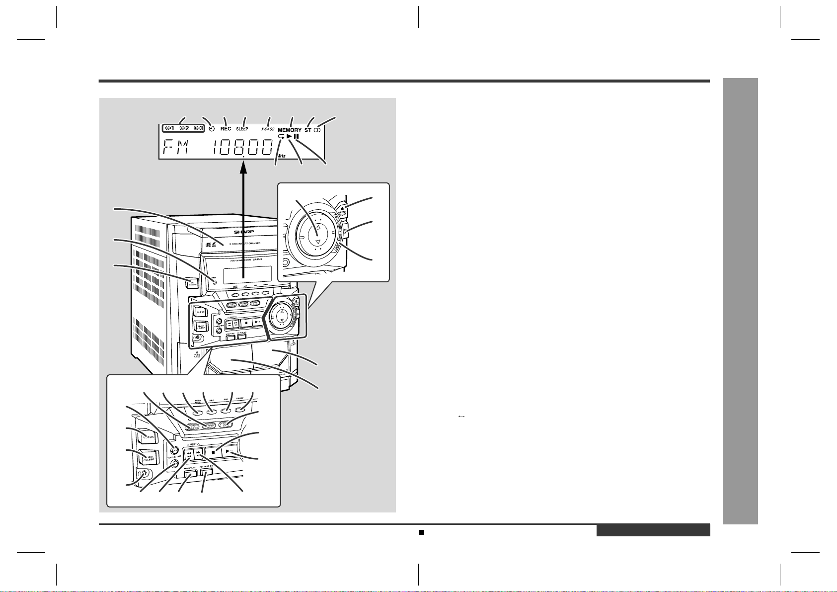
NAMES OF PARTS
■ Display
1. Disc Number Indicators
2. Timer Indicator
3. Tape 2 Record Indicator
4. Sleep Indicator
5. Extra Bass Indicator
6. Disc or Tuner Memory Indicator
7. FM Stereo Mode Indicator
8. FM Stereo Receiving Indicator
9. Disc Repeat Play Indicator
10. Disc or Tape Play Indicator
11. Disc Pause Indicator
■ Front panel
1. Disc Tray
2. Timer Set Indicator
3. On/Stand-by Button
4. Volume Up and Down Buttons
5. Disc Tray Open/Close Button
6. Disc Skip Button
7. Equaliser Mode Select/Extra Bass/Demo Mode Button
8. Tape 2 Cassette Compartment
9. Tape 1 Cassette Compartment
10. Video CD/CD Button
11. Tuner (Band) Button
12. Audio Mode Button
13. Video CD Playback Control Button
14. Video CD On Screen Display On/Off Button
15. Video CD Digest/Time Search Button
16. Tuning and Time Up Button
17. Clock Button
18. Timer/Sleep Button
19. Headphone Socket
20. Tape (1 2) Button
21. Video CD Stop or Return, CD/Tape Stop Button
22. Video CD Play or Repeat or Select or Resume, CD Play or Repeat
Tape Play Button
23. Tuning and Time Down Button
24. Video CD Skip or Previous, CD Track Down or Fast Reverse,
Tape 2 Rewind, Tuner Preset Down Button
25. Memory/Set Button
26. Tape 2 Record Pause Button
27. Video CD Skip or Next, CD Track Up or Fast Forward,
Tape 2 Fast Forward, Tuner Preset Up Button
28. Microphone Level Control
29. Microphone Socket
1. Disc Tray
2. Timer Set Indicator
3. On/Stand-by Button
4. Volume Up and Down Buttons
5. Disc Tray Open/Close Button
6. Disc Skip Button
7. Equaliser Mode Select/Extra Bass/Demo Mode Button
8. Tape 2 Cassette Compartment
9. Tape 1 Cassette Compartment
10. Video CD/CD Button
11. Tuner (Band) Button
12. Audio Mode Button
13. Video CD Playback Control Button
14. Video CD On Screen Display On/Off Button
15. Video CD Digest/Time Search Button
16. Tuning and Time Up Button
17. Clock Button
18. Timer/Sleep Button
19. Headphone Socket
20. Tape (1 2) Button
21. Video CD Stop or Return, CD/Tape Stop Button
22. Video CD Play or Repeat or Select or Resume, CD Play or Repeat
Tape Play Button
23. Tuning and Time Down Button
24. Video CD Skip or Previous, CD Track Down or Fast Reverse,
Tape 2 Rewind, Tuner Preset Down Button
25. Memory/Set Button
26. Tape 2 Record Pause Button
27. Video CD Skip or Next, CD Track Up or Fast Forward,
Ta
p
e 2 Fast Forward, Tuner Preset U
p
Button
8
9
1
2
3
4
5
6
7
18
2523
17
13 14 15121110
16
27
24
29
26
28
19
20
21
22
123 4 5 6 7 8
11109
8
9
1
2
3
4
5
6
7
18
2523
17
13 14 15121110
16
27
24
26
19
20
21
22
For CD-BP99V
For CD-BK110V
CD-BK110V/CD-BP99V
– 5 –
CD-BK110V/CD-BP99V
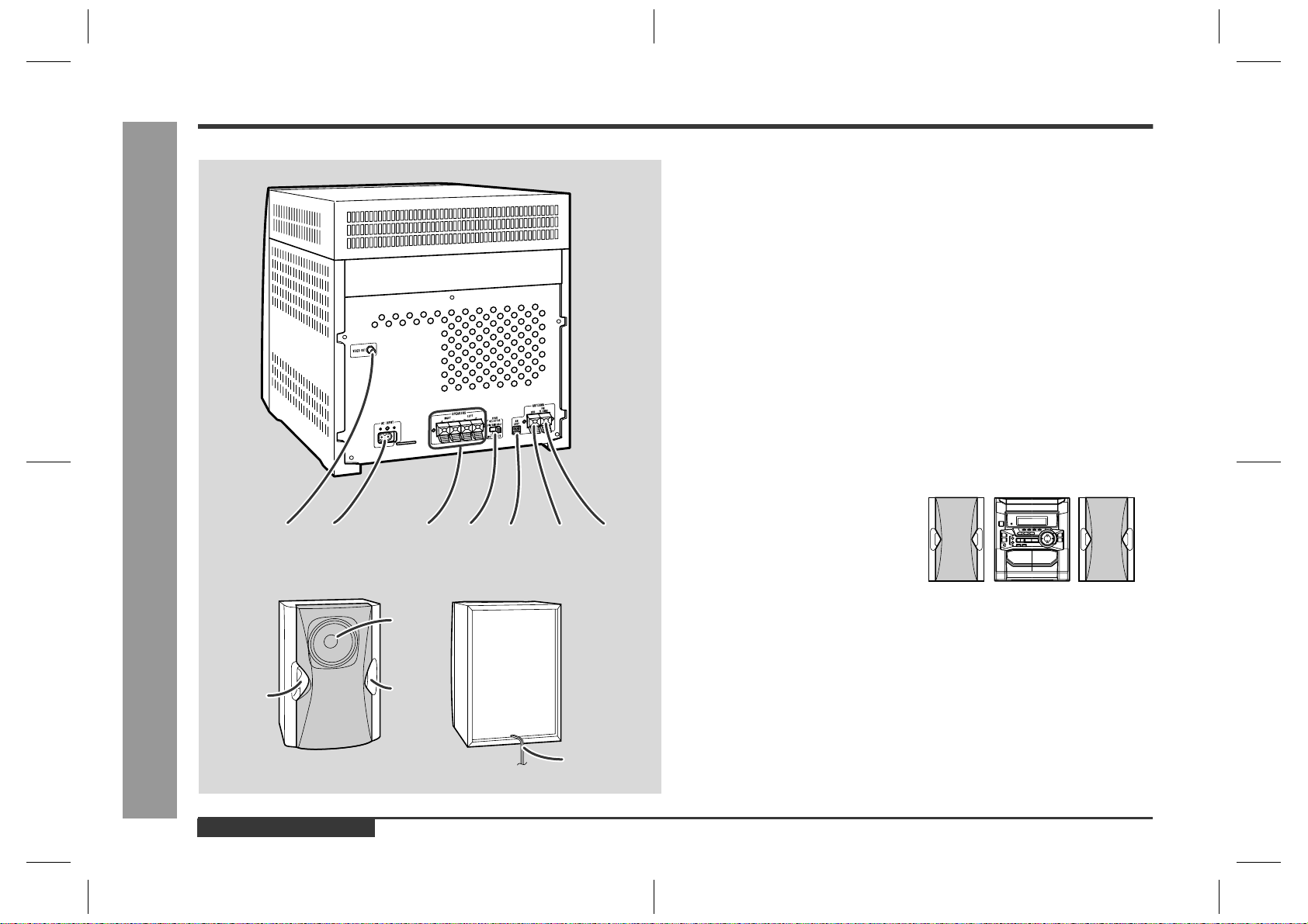
■ Rear panel
1. Video Output Socket
2. AC Power Input Socket
3. AC Voltage Selector
4. Speaker Terminals
5. Span Selector Switch
6. AM Loop Aerial Socket
7. FM Aerial Earth Terminal
8. FM 75 Ohms Aerial Terminal
1. Video Output Socket
2. AC Power Input Socket
3. Speaker Terminals
4. Span Selector Switch
5. AM Loop Aerial Socket
6. FM Aerial Earth Terminal
7. FM 75 Ohms Aerial Terminal
■ Speaker system
1. Full-Range Speaker
2. Bass Reflex Duct
3. Speaker Wire
2
1
2
3
321
67854
21
56743
CP-BK110/CP-BP99
For CD-BP99V
For CD-BK110V
CD-BK110V/CD-BP99V
– 6 –
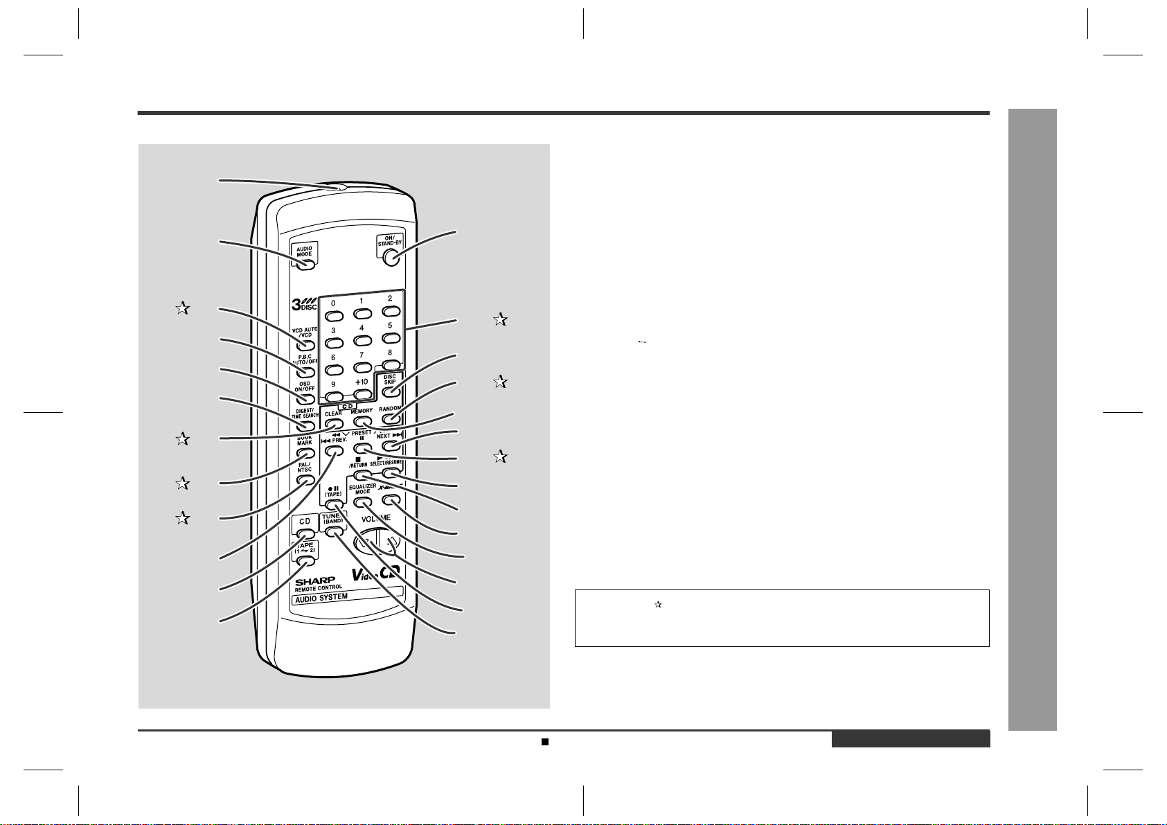
■ Remote control
1. Remote Control Transmitter
2. Audio Mode Button
3. Video CD Auto/On Button
4. Video CD Playback Control Auto/Off Button
5. Video CD On Screen Display On/Off Button
6. Video CD Digest/Time Search Button
7. CD Clear Button
8. Video CD Bookmark Button
9. PAL/NTSC Select Button
10. Video CD Skip or Previous, CD Track Down or Fast Reverse,
Tape 2 Rewind, Tuner Preset Down Button
11. Video CD/CD Button
12. Tape (1 2) Button
13. On/Stand-by Button
14. Disc Direct Search Buttons
15. Disc Skip Button
16. Disc Random Button
17. Disc Memory Button
18. Video CD Skip or Next, CD Track Up or Fast Forward,
Tape 2 Fast Forward, Tuner Preset Up Button
19. Disc Pause Button
20. Video CD Play or Repeat or Select or Resume, CD Play or Repeat,
Tape Play Button
21. Video CD Stop or Return, CD/Tape Stop Button
22. Extra Bass Button
23. Equalizer Mode Select Button
24. Volume Up and Down Buttons
25. Tape 2 Record Pause Button
26. Tuner (Band) Button
Buttons with " " mark in the illustration can be operated on the remote control
only.
Other buttons can be operated both on the main unit and the remote control.
1
2
14
16
15
17
19
18
20
24
6
3
4
5
7
8
9
10
25
13
22
21
23
26
12
11
CD-BK110V/CD-BP99V
– 7 –
CD-BK110V/CD-BP99V
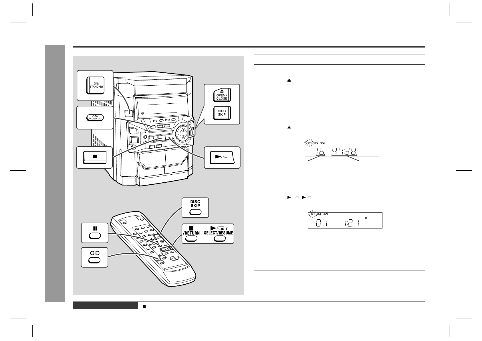
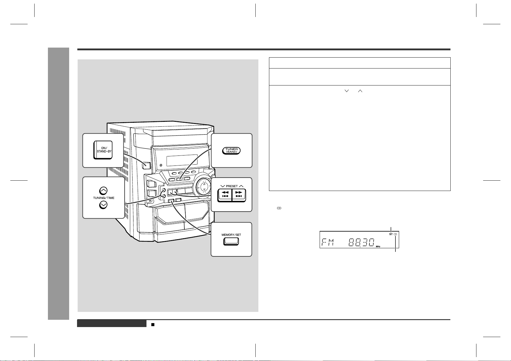
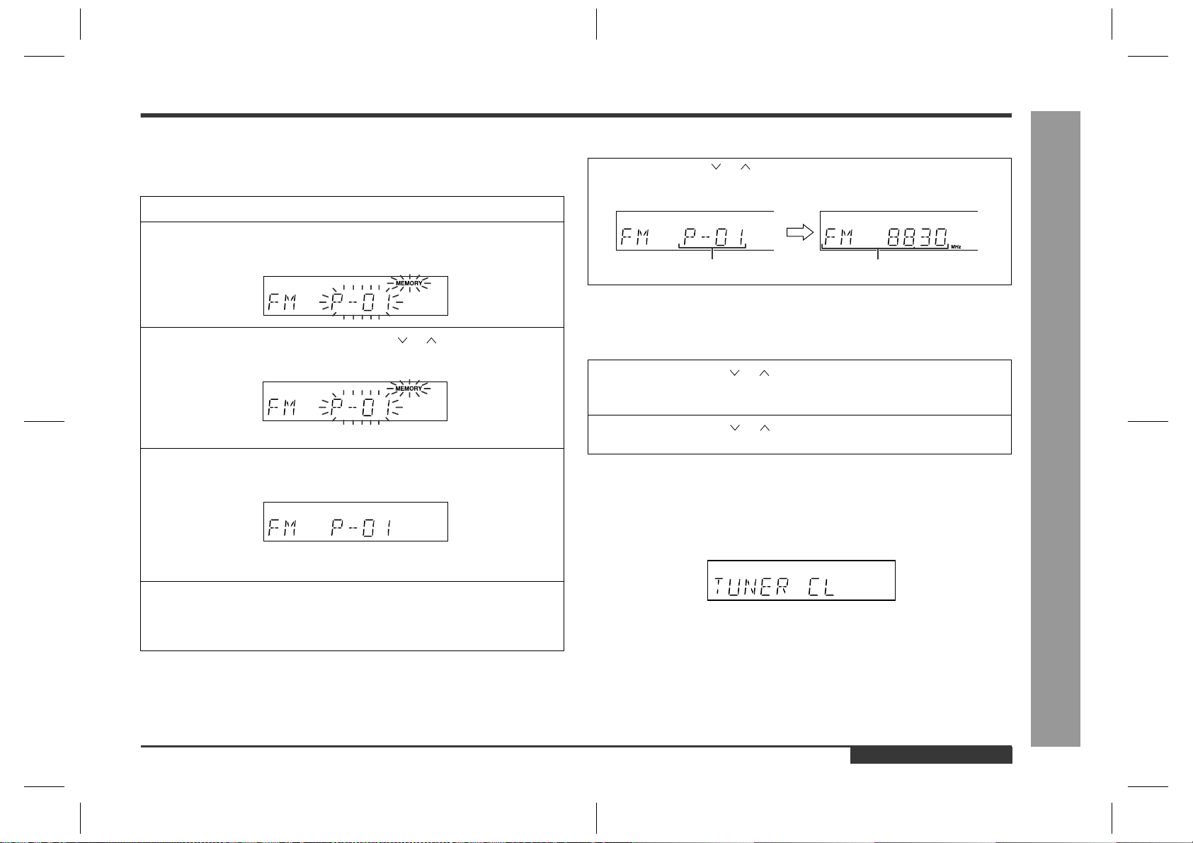
OPERATION MANUAL
1
2
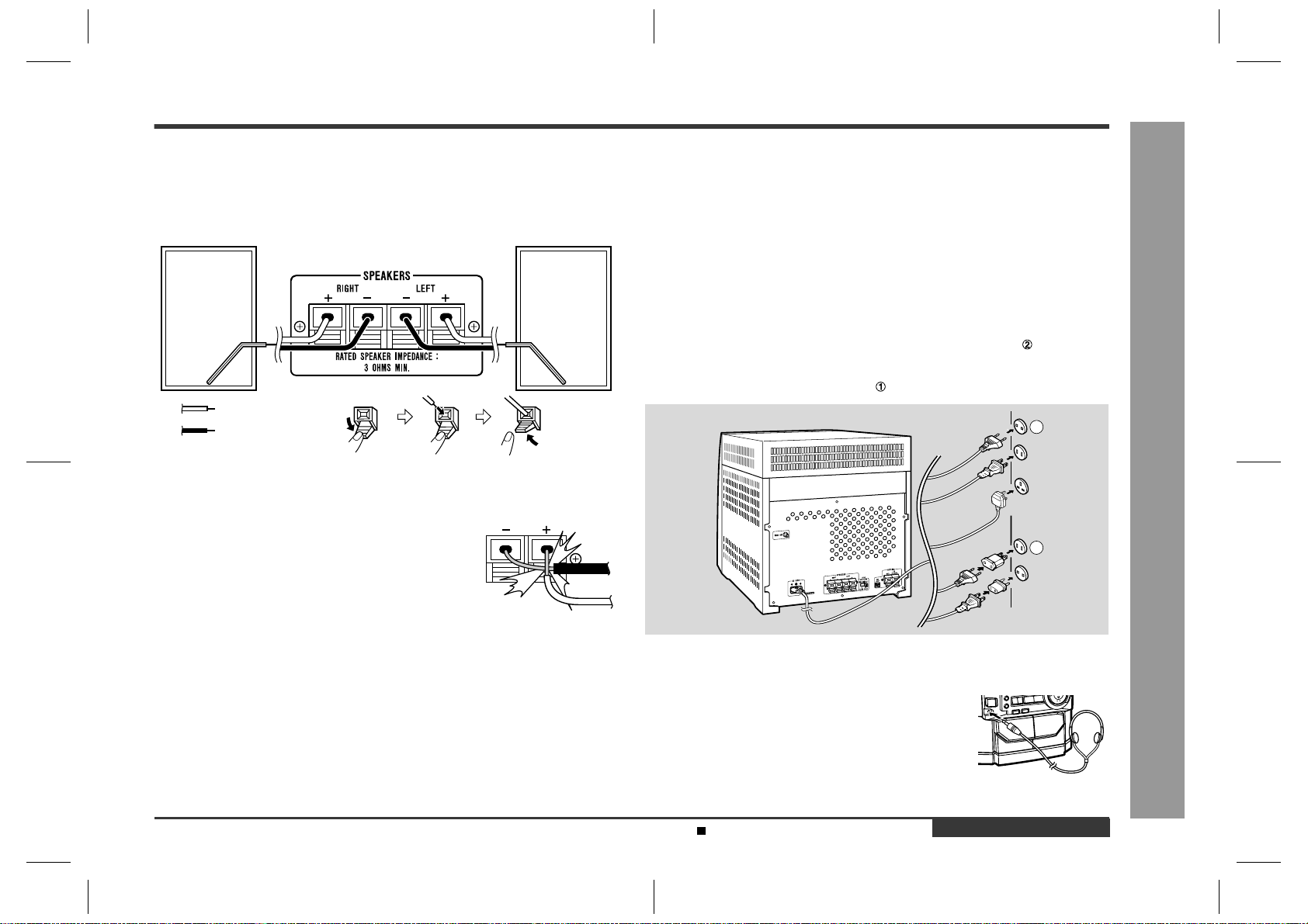
Setting the AC voltage selector
Check the setting of the AC voltage selector located on the rear panel before plug-
ging the unit into an AC socket. If necessary, adjust the selector to correspond to the
AC power voltage used in your area.
Turn the selector with a screwdriver until the appropriate voltage num-
ber appears in the window (110 V, 127 V, 220 V or 230 V - 240 V AC).
Connecting the AC power lead
After making all connections, connect the AC power lead to the unit
and then into the wall socket. If you plug in the unit first, it will enter
the demonstration mode.
Notes:
Unplug the AC power lead from the AC socket if the unit will not be in use for a pro-
longed period of time.
Never use a power lead other than the one supplied. Use of a power lead
other than the one supplied may cause an electric shock or fire.
AC Plug Adaptor
In areas (or countries) where an AC socket as shown in illustration is used, con-
nect the unit using the AC plug adaptor supplied with the unit, as illustrated. The AC
plug adaptor is not included in areas where the AC wall socket and AC power plug
can be directly connected (see illustration ).
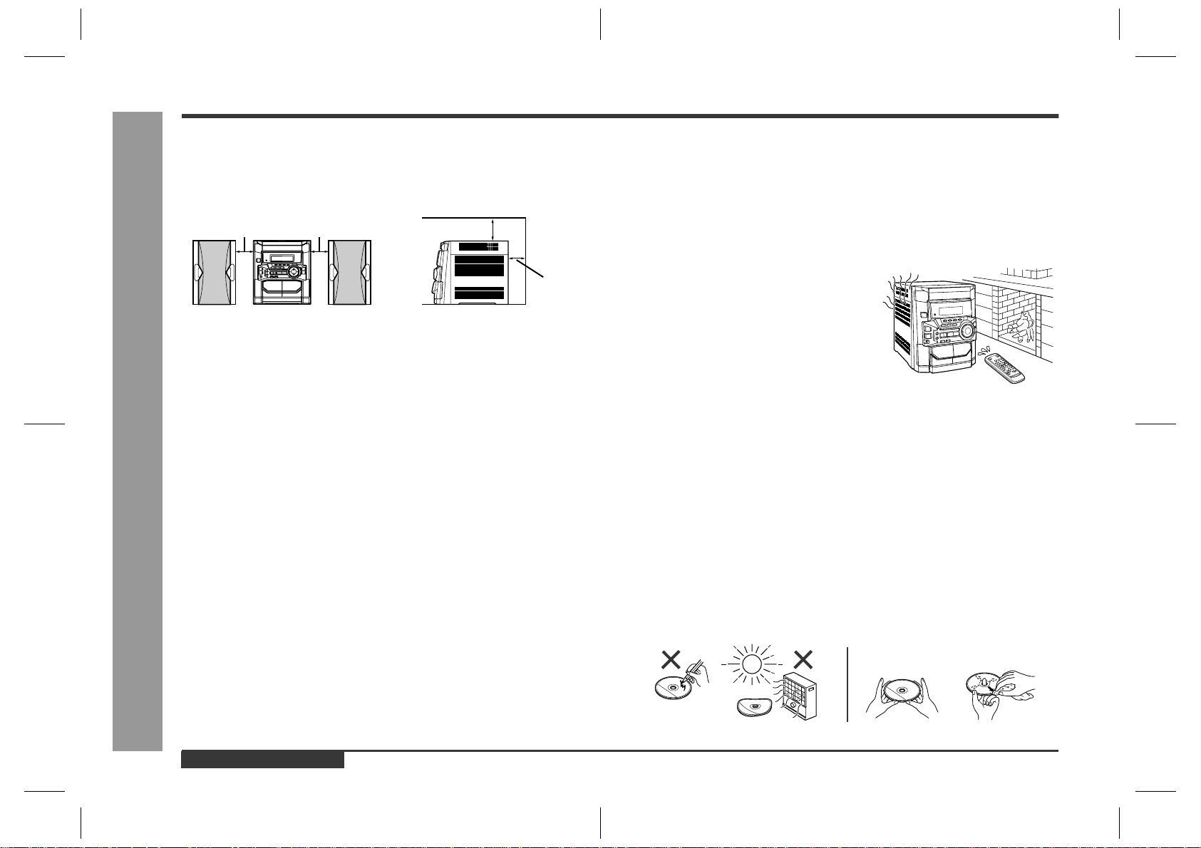
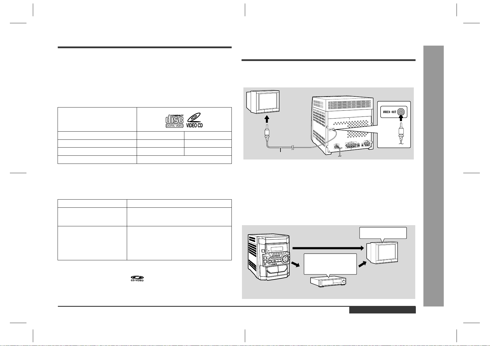
System Connections (For CD-BK110V)
Setting the FM/AM Span Selector
The International Telecommunication Union (ITU) has established that member coun-
tries should maintain either a 100 kHz or a 50 kHz interval between broadcasting fre-
quencies of FM stations and 10 kHz or 9 kHz for AM station. The illustration shows
the 50/9 kHz zones (regions 1 and 3), and the 100/10 kHz zone (region 2).
Before using the unit, set the SPAN SELECTOR switch (on the rear panel) to the
interval (span) of your area.
To change the tuning zone:
Caution:
This operation will erase all data stored in memory including clock, timer settings,
tuner preset, and CD programme.
1 Press the ON/STAND-BY button to enter the stand-by mode.
2 Set the SPAN SELECTOR switch (on the rear panel) as follows.
For 50 kHz FM interval (9 kHz in AM) 50/9
For 100 kHz FM interval (10 kHz in AM) 100/10
3 Whilst pressing down the / button and the EQUALIZER/X-BASS/DEMO button,
press the ON/STAND-BY button until "CLEAR AL" appears.
Connecting the AC power lead
After making all connections, connect the AC power lead to the unit
and then into the wall socket. If you plug in the unit first, it will enter
the demonstration mode.
Notes:
Unplug the AC power lead from the AC socket if the unit will not be in use for a pro-
longed period of time.
Never use a power lead other than the one supplied. Use of a power lead
other than the one supplied may cause an electric shock or fire.
AC Plug Adaptor
In areas (or countries) where an AC socket as shown in illustration is used, con-
nect the unit using the AC plug adaptor supplied with the unit, as illustrated. The AC
plug adaptor is not included in areas where the AC wall socket and AC power plug
can be directly connected (see illustration ).
System Connections (For CD-BP99V)
Setting the FM/AM Span Selector
The International Telecommunication Union (ITU) has established that member coun-
tries should maintain either a 100 kHz or a 50 kHz interval between broadcasting fre-
quencies of FM stations and 10 kHz or 9 kHz for AM station. The illustration shows
the 50/9 kHz zones (regions 1 and 3), and the 100/10 kHz zone (region 2).
Before using the unit, set the SPAN SELECTOR switch (on the rear panel) to the
interval (span) of your area.
To change the tuning zone:
Caution:
This operation will erase all data stored in memory including clock, timer settings,
tuner preset, and CD programme.
1 Press the ON/STAND-BY button to enter the stand-by mode.
2 Set the SPAN SELECTOR switch (on the rear panel) as follows.
For 50 kHz FM interval (9 kHz in AM) 50/9
For 100 kHz FM interval (10 kHz in AM) 100/10
3 Whilst pressing down the / button and the EQUALIZER/X-BASS/DEMO button,
press the ON/STAND-BY button until "CLEAR AL" appears.
1
2
CD-BK110V/CD-BP99V
– 8 –
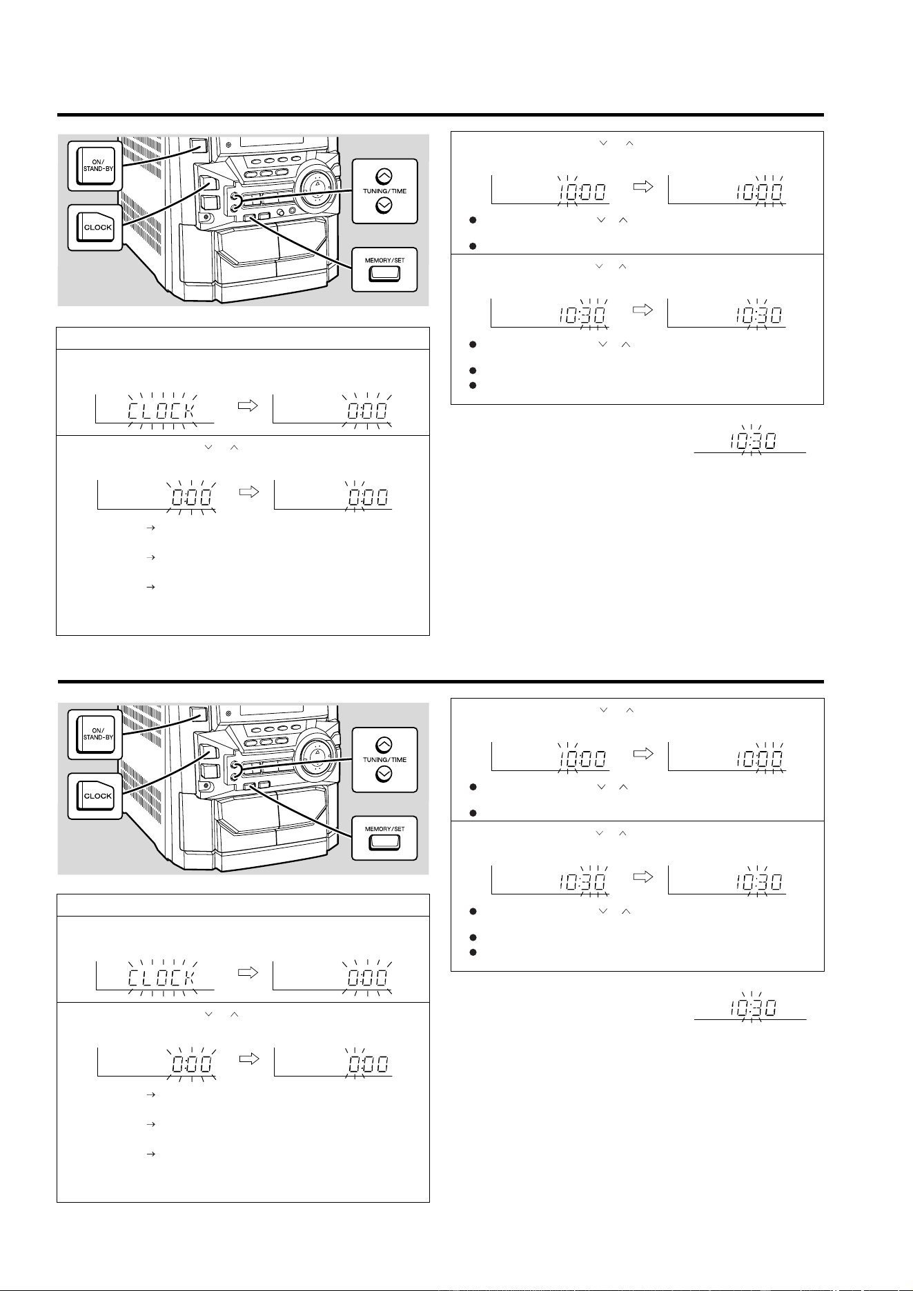
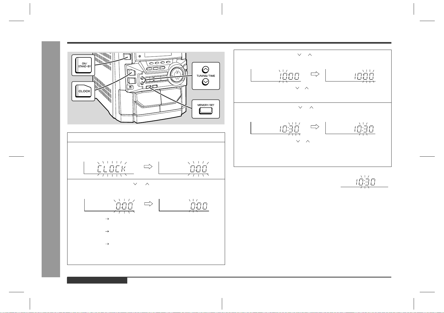
Setting the Clock (For CD-BK110V)
In this example, the clock is set for the 24-hour (0:00) display.
Note:
The "CLOCK" or time will flash at the push of the CLOCK button when the AC power
supply is restored after a power failure or unplugging the unit.
Readjust the clock as follows.
To readjust the clock:
Perform "Setting the Clock" from the beginning. If the time display is flashing, step 3
(for selecting the 24-hour or 12-hour display) will be skipped.
To change the 24-hour or 12-hour display:
1
Press the ON/STAND-BY button to turn the power on.
2
Press the CLOCK button and within 5 seconds, press the MEMORY/
SET button.
3
Press the TUNING/TIME ( or ) button to select 24-hour or 12-hour
display and then press the MEMORY/SET button.
"0:00" The 24-hour display will appear.
(0:00 - 23:59)
"AM 12:00" The 12-hour display will appear.
(AM 12:00 - PM 11:59)
"AM 0:00" The 12-hour display will appear.
(AM 0:00 - PM 11:59)
Note that this can only be set when the unit is first installed or it has been reset.
[Refer to "Clearing all the memory (reset)".]
4
Press the TUNING/TIME ( or ) button to adjust the hour and then
press the MEMORY/SET button.
Press the TUNING/TIME ( or ) button once to advance the time by 1 hour.
Hold it down to advance continuously.
When the 12-hour display is selected, "AM" will change automatically to "PM".
5
Press the TUNING/TIME ( or ) button to adjust the minutes and then
press the MEMORY/SET button.
Press the TUNING/TIME ( or ) button once to advance the time by 1
minute. Hold it down to change the time in 5-minute intervals.
The hour will not advance even if minutes advance from "59" to "00".
The clock begins counting from "0" seconds. (Seconds are not displayed.)
The time display will disappear after a few seconds.
To confirm the time display:
Press the CLOCK button.
The time display will appear for about 5 seconds.
1 Clear all the programmed contents. [Refer to "Clearing all the memory (reset)".]
2 Perform "Setting the Clock" from the beginning.
Setting the Clock (For CD-BP99V)
In this example, the clock is set for the 24-hour (0:00) display.
Note:
The "CLOCK" or time will flash at the push of the CLOCK button when the AC power
supply is restored after a power failure or unplugging the unit.
Readjust the clock as follows.
To readjust the clock:
Perform "Setting the Clock" from the beginning. If the time display is flashing, step 3
(for selecting the 24-hour or 12-hour display) will be skipped.
To change the 24-hour or 12-hour display:
1
Press the ON/STAND-BY button to turn the power on.
2
Press the CLOCK button and within 5 seconds, press the MEMORY/
SET button.
3
Press the TUNING/TIME ( or ) button to select 24-hour or 12-hour
display and then press the MEMORY/SET button.
"0:00" The 24-hour display will appear.
(0:00 - 23:59)
"AM 12:00" The 12-hour display will appear.
(AM 12:00 - PM 11:59)
"AM 0:00" The 12-hour display will appear.
(AM 0:00 - PM 11:59)
Note that this can only be set when the unit is first installed or it has been reset.
[Refer to "Clearing all the memory (reset)".]
4
Press the TUNING/TIME ( or ) button to adjust the hour and then
press the MEMORY/SET button.
Press the TUNING/TIME ( or ) button once to advance the time by 1 hour.
Hold it down to advance continuously.
When the 12-hour display is selected, "AM" will change automatically to "PM".
5
Press the TUNING/TIME ( or ) button to adjust the minutes and then
press the MEMORY/SET button.
Press the TUNING/TIME ( or ) button once to advance the time by 1
minute. Hold it down to change the time in 5-minute intervals.
The hour will not advance even if minutes advance from "59" to "00".
The clock begins counting from "0" seconds. (Seconds are not displayed.)
The time display will disappear after a few seconds.
To confirm the time display:
Press the CLOCK button.
The time display will appear for about 5 seconds.
1 Clear all the programmed contents. [Refer to "Clearing all the memory (reset)".]
2 Perform "Setting the Clock" from the beginning.
– 9 –
CD-BK110V/CD-BP99V
Troubleshooting
If trouble occurs
When this product is subjected to strong external interference (mechanical shock,
excessive static electricity, abnormal supply voltage due to lightning, etc.) or if it is
operated incorrectly, it may malfunction.
If such a problem occurs, do the following:
1 Set the unit to the stand-by mode and turn the power on again.
2 If the unit is not restored in the previous operation, unplug and plug in the unit,
and then turn the power on.
Note:
If neither operation above restores the unit, clear all the memory by resetting it.
Clearing all the memory (reset)
1 Press the ON/STAND-BY button to enter the power stand-by mode.
2 Whilst pressing down the / button and the EQUALIZER/X-BASS/DEMO but-
ton, press the ON/STAND-BY button until "CLEAR AL" appears.
Caution:
This operation will erase all data stored in memory including clock, timer settings,
tuner preset, and CD programme.
Before transporting the unit
1 Press the ON/STAND-BY button to turn the power on.
2 Press the CD/VIDEO CD button.
3 Press the OPEN/CLOSE button to open the disc tray.
Remove all discs from the unit.
4 Press the OPEN/CLOSE button to close the disc tray.
Make sure that "NO DISC" is displayed.
5 Press the ON/STAND-BY button to enter the stand-by mode, and then unplug
the AC power lead from the AC socket.
Remote Control (For CD-BK110V)
Test of the remote control
Face the remote control directly to the remote
sensor on the unit.
The remote control can be used within
the range shown:
Press the ON/STAND-BY button. Does the
power turn on? Now, you can enjoy the music.
Remote Control (For CD-BP99V)
Test of the remote control
Face the remote control directly to the remote
sensor on the unit.
The remote control can be used within
the range shown:
Press the ON/STAND-BY button. Does the
power turn on? Now, you can enjoy the music.
Remote sensor
0.2 m - 6 m
(8" - 20')
Remote sensor
0.2 m - 6 m
(8" - 20')
CD-BK110V/CD-BP99V
– 10 –
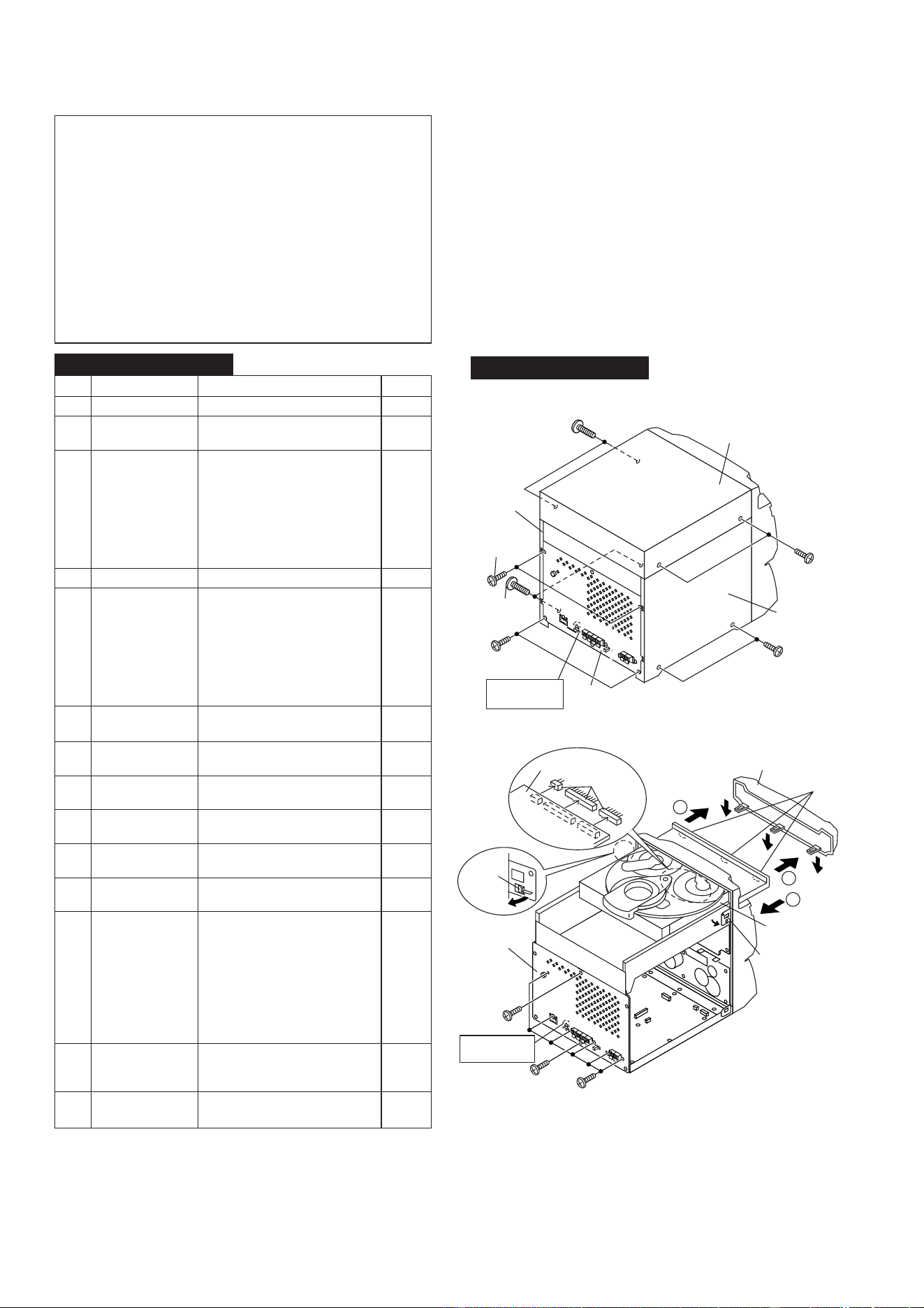
1 Top Cabinet 1. Screw ...................... (A1) x4 10-1
2 Side Panel 1. Screw ...................... (B1) x8 10-1
(Left/Right)
3 CD Tray Cover/ 1. Turn on the power supply, .. 10-2
CD Player Unit open the disc tray, take out
the CD tray cover, and close.
(Note 1)
2. Hook ........................ (C1) x3
3. Screw ...................... (C2) x1
4. Hook ........................ (C3) x2
5. Socket ..................... (C4) x3
4 Rear Panel 1. Screw ...................... (D1) x7 10-2
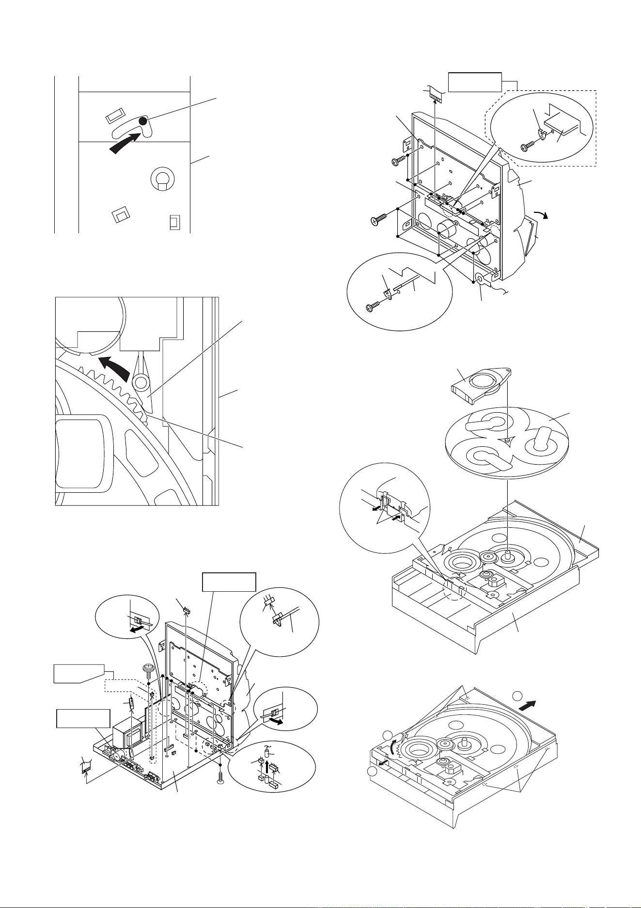
5 Front Panel 1. Flat Cable ............... (E1) x1 11-3
2. Socket ..................... (E2) x4
(For CD-BK110V)
2. Socket ..................... (E2) x3
(For CD-BP99V)
3. Tip ........................... (E3) x1
4. Screw ...................... (E4) x3
5. Hook ........................ (E5) x2
6 Main PWB 1. Socket ......................(F1) x2 11-3
2. Screw .......................(F2) x7
7 Mic PWB 1. Screw ...................... (G1) x1 11-4
(CD-BK110V Only)
2. Bracket .................... (G2) x1
8 Display PWB 1. Screw .................... (H1) x11 11-4
2. Flat Wire.................. (H2) x1
9
Headphones PWB
1. Screw ....................... (J1) x1 11-4
2. Bracket ..................... (J2) x1
10 Tape Mechanism 1. Open the cassette holder. .. 11-4
2. Screw...................... (K1) x6
11 Turntable 1. Hook ......................... (L1) x2 11-5
2. Cover ....................... (L2) x1
12 Disc Tray 1.
Turn fully the lock lever in the
11-1
arrow direction
.
2.
While holding the lock lever,rotate
11-2
the cam gear until the cam gear
rib engages with the clamp lever.
3.
Push the slide chassis backward
11-6
to engage the claw with the
groove and remove it in the
direction of the arrow
..
(M1) x6
13 VIDEO CD PWB 1. Screw ...................... (N1) x1 12-1
(Note 2) 2. Socket ..................... (N2) x4
3. Hook ........................ (N3) x2
14 CD Mechanism 1. Hook ........................ (P1) x2 12-2
2. Hook ........................ (P2) x3
DISASSEMBLY
Caution on Disassembly
Follow the below-mentioned notes when disassembling
the unit and reassembling it, to keep it safe and ensure
excellent performance:
1. Take cassette tape and compact disc out of the unit.
2. Be sure to remove the power supply plug from the wall
outlet before starting to disassemble the unit.
3. Take off nylon bands or wire holders where they need to
be removed when disassembling the unit. After servicing
the unit, be sure to rearrange the leads where they were
before disassembling.
4. Take sufficient care on static electricity of integrated
circuits and other circuits when servicing.
Figure 10-2
STEP
REMOVAL
PROCEDURE
FIGURE
Figure 10-1
Note 1: How to open the changer manually. (Fig. 11-1)
1. In this state, turn fully the lock lever in the arrow direction through
the hole on the loading chassis bottom.
2.
While holding the lock lever, rotate the cam gear anticlockwise until the
cam gear rib engages with the clamp lever.
(Fig. 11-2)
3. After that, push forward the slide chassis.
Note 2:
1. After removing the connector for the optical pickup from the
connector, wrap the conductive aluminium foil around the front end
of the connector so as to protect the optical pickup from electro-
static damage.
Note 3:
1. Be careful not to break the claw of the CD mechanism.
2. When fining back the cam gear assembly, let it lock by front
movement.
Illustration: CD-BK110V
(A1) x 2
ø3 x 12mm
(B1) x 2
ø3 x 7mm
(B1) x 2
ø3 x 7mm
Rear
Panel
(B1) x 2
ø3 x 7mm
Side Panel
(Right)
Side Panel
(Left)
(A1) x 2
ø3 x 12mm
Top Cabinet
(B1) x 2
ø3 x 10mm
CD-BK110V
ONLY
Pull
Pull
(C3) x 1
(C4) x 3
VIDEO CD
PWB
CD Tray Cover
(C1) x 3
1
1
2
(C3) x 1
CD Player
Unit
(D1) x 6
ø3 x 10mm
(C2) x 1
ø3 x 10mm
Rear
Panel
(D1) x 1
ø3 x 7mm
CD-BK110V
ONLY
CD-BK110V/CD-BP99V
CD-BK110V/CD-BP99V
– 11 –
CD-BK110V/CD-BP99V
Figure 11-1
Figure 11-2
Figure 11-3
Figure 11-4
Figure 11-5
Figure 11-6
Lock Lever
CD Player Unit
(Bottom View)
Clamp Lever
CD Player Unit
(Top View)
Cam Gear Rib
(E1) x 1
(F2) x 7
ø3 x 10mm
(E2) x 1
Front
Panel
(E4) x 3
ø3 x 8mm
Main PWB
Headphones
PWB
(E3) x 1
(E5) x 1
Pull
(E2) x 1
(F1) x 1
(E2) x 1
(F1) x 1
(E2) x 1
(E5) x 1
Pull
CD-BK110V
ONLY
CD-BK110V
ONLY
CD-BK110V
ONLY
Mic PWB
(G1) x 1
ø3 x 10mm
Open
Cassette
Holder
Lug Wire
Headphones
PWB
(J1) x 1
ø3 x 10mm
(K1) x 6
ø3 x 10mm
Tape
Mechanism
(H1) x 11
ø3 x 10mm
Display
PWB
Front
Panel
(H2) x 1
(G2) x 1
(J2) x 1
CD-BK110V
ONLY
Turntable
Slide
Chassis
(L2) x 1
CD Player Unit
(L1) x 2
3
(M1) x 3
(M1) x 3
1
2
CD-BK110V/CD-BP99V
– 12 –
Figure 12-1
Figure 12-2
(N2) x 2
(N3) x 2
(N2) x 2
VIDEO CD
PWB
Slide
Chassis
(N1) x 1
ø3 x 8mm
(P2) x 3
(P1) x 1
(P1) x 1
Slide
Chassis
CD
Mechanism
These speakers CP-BK110/CP-BP99 are available in
assemblies only and may not be disassembled.
CP-BK110/CP-BP99
– 13 –
CD-BK110V/CD-BP99V
REMOVING AND REINSTALLING THE MAIN PARTS
TAPE MECHANISM SECTION
Perform steps 1 to 5 and 10 of the disassembly method to
remove the tape mechanism. (See page 10.)
How to remove the record/playback and erase
heads (TAPE 2) (See Fig. 13-1)
1. When you remove the screws (A1) x 2 pcs., the recording/
playback head and three-dimensional head of the erasing
head can be removed.
How to remove the playback head (TAPE 1)
(See Fig. 13-2)
1. When you remove the screws (B1) x 2 pcs., the playback
head can be removed.
How to remove the pinch roller (TAPE 1/2)
(See Fig. 13-3)
1. Carefully bend the pinch roller pawl in the direction of the
arrow <A>, and remove the pinch roller (C1) x 1 pc., in the
direction of the arrow <B>.
Note:
When installing the pinch roller, pay attention to the spring
mounting position.
How to remove the belt (TAPE 2) (See Fig. 13-4)
1. Remove the main belt (D1) x 1 pc., from the motor side.
2. Remove the FF/REW belt (D2) x 1 pc.
How to remove the belt (TAPE 1) (See Fig. 13-4)
1. Remove the main belt (E1) x 1 pc., from the motor side.
2. Remove the FF/REW belt (E2) x 1 pc.
How to remove the motor (See Fig. 13-5)
1. Remove the screws (F1) x 2 pcs., to remove the motor.
Figure 13-1
Figure 13-2
Figure 13-3
Figure 13-4Figure 13-5
(A1) x 2
Ø2 x 9mm
TAPE 2
Record/Playback
Head
Erase Head
Clutch Ass'y
(B1) x 2
Ø2 x 9mm
TAPE 1
Playback
Head
Clutch Ass'y
Pinch Roller
(C1) x 1
<A>
<B>
Pinch
Roller
Pawl
Pull
TAPE 2
TAPE 1
Main Belt
(E1) x 1
TAPE 2
Main Belt
(D1) x 1
TAPE 1
Main Belt
(D1) x 1
FF/REW
Belt
(D2) x 1
FF/REW
Belt
(E2) x 1
Motor
Motor
(F1) x 2
Ø2.6 x 5mm
Motor
Clutch Ass'y
CD-BK110V/CD-BP99V
– 14 –
How to remove the pickup (See Fig. 14-2)
1. Remove the stop washer (B1) x 1 pc., to remove the gear
(B2) x 1 pc.
2. Remove the screws (B3) x 2 pcs., to remove the shaft
(B4) x 1 pc.
3. Remove the pickup.
Note
After removing the connector for the optical pickup from the
connector wrap the conductive aluminium foil around the front
end of connector so as to protect the optical pickup from
electrostatic damage.
Figure 14-2
CD MECHANISM SECTION
Perform steps 1, 2, 3, 11,12, 13 and 14 of the disassembly
method to remove the CD mechanism. (See page 10.)
How to remove the loading motor
(See Fig. 14-1)
1. Bend the hooks (A1) x 5 pcs., to remove the loading motor.
2. Remove the drive belt (A2) x 1pc.
Figure 14-1
ADJUSTMENT
MECHANISM SECTION
• Driving Force Check
Torque Meter Specified Value
Play: TW-2111 Tape 1: Over 80 g
Tape 2: Over 80 g
• Torque Check
Torque Meter
Tape 2
Play: TW-2111 30 to 80 g.cm 30 to 80 g.cm
Fast forward: TW-2231 — 70 to 180 g.cm
Rewind: TW-2231 — 70 to 180 g.cm
Specified Value
Tape 1
Specified
Value
Adjusting
Point
Instrument
Connection
Test Tape
Normal MTT-111 Variable 3,000 ± 30 Hz Speaker
speed Resistor in Terminal
motor. (Load
resistance:
6 ohms)
• Tape Speed
Figure 14-3
(A1) x 2
(A1) x 1
Loading Motor
Loading
Motor PWB
Slide
Chassis
(A1) x 2
Pulley
Drive Belt
(A2) x 1
Loading
Motor
(B3) x 2
ø2.6 x 6mm
Shaft
(B4) x 1
Stop Washer
(B1) x 1
Gear
(B2) x 1
CD Mechanism
Pickup
TAPE MECHANISM
Tape
Motor
Variable Resistor in motor
– 15 –
CD-BK110V/CD-BP99V
Figure 15-2
CD ERROR CODE DESCRIPTION
Error State Code
[Servo System Error]
0001 Cannot detect Pickup-in SW
0002 DSP access error
[Error during close operation]
0101 Open/Close SW not functioning (Low → High)
0103 Open/Close SW not functioning (High → Low)
[Error during open operation]
0201 Open/Close SW not functioning (Low → High)
0203 Open/Close SW not functioning (High → Low)
[Error during skip operation]
0302 Pickup-in SW is not detected
0306 During Disc 1 search, Open/Close SW or Clamp SW
or Disc SW do not change to low.
0307 Clamp SW not function (Low → High)
0308 Clamp SW not function (High → Low)
T
T
EFBL
FDO
TE
Stopped
CH1=500 mV
DC 10:1
CH2=200 mV
DC 10:1
CH3=1 V
DC 10:1
500 ms/div
(500 ms/div)
NORM:20 kS/s
1
2
3
=Record Length=
Smoothing : ON CH1 : 0.000 V
CH2 : 0.000 V
Main : 100 K
Zoom : 2 k
Mode : SINGLE
Type : EDGE CH1
Delay : 0.0 ns
Hold off : 0.2 µs
CH3 : 0.00 V
CH4 : 0.00 V
BW : FULL
=Trigger==Filter= =Offset=
CH2
v/DIV
200 mV
1999/04/05 20:26:47
Test Stage
Frequency Frequency
Display
Setting/
Adjusting
Parts
Instrument
Connection
CD SECTION
• AM IF/RF
Signal generator: 400 Hz, 30%, AM modulated
*1. Input: Antenna Output: TP302
*2. Input: Antenna Output: TP301
TUNER SECTION
fL: Low-range frequency
fH: High-range frequency
AM IF 450 kHz 1,602 kHz T351 *1
AM Band — 531 kHz (fL): T306 *2
Coverage 1.1 ± 0.1 V
AM Tracking 990 kHz 990 kHz (fL): T303 *1
*1. Input: Antenna Output: TP301
*2. Input: Antenna Output: Speaker terminal
• FM RF
Signal generator: 1 kHz, 40 kHz dev., FM modulated
FM Band — 87.50 MHz T301(fL): *1
Coverage 1.3 V ± 0.1 V
FM RF 98.00 MHz 98.00 MHz L312 *2
(10-30 dB)
Test Stage
Instrument
Connection
Frequency Frequency
Display
Setting/
Adjusting
Point
Figure 15-1 ADJUSTMENT POINTS
Items adjusted automatically
(1) Offset adjustment (The offset voltage between the head
amplifier output and the VREF reference voltage is
compensated inside the IC.)
* Focus offset adjustment
* Tracking offset adjustment
(2) Tracking balance adjustment (waveform drawing
Fig.15-2 EFBL)
(3) Gain adjustment (The gain is compensated inside the IC
so that the loop gain at the gain crossover frequency will
be 0 dB.)
* Focus gain adjustment
* Tracking gain adjustment
• Adjustment
Since this CD system incorporates the following automatic
adjustment functions, readjustment is not needed when
replacing the pickup. Therefore, different PWBs and pickups
can be combined freely.
Each time a disc is changed, these adjustments are
performed automatically. Therefore, playback of each disc
can be performed under optimum conditions.
• FM IF
Signal generator: 10.7 MHz, FM modulated
IF 10.7 MHz 98 MHz T302 *1
(Turn the
core of trans-
former T302
fully counter-
clock wise)
Test Stage
Instrument
Connection
Frequency Frequency
Display
Setting/
Adjusting
Point
*1. Input: Antenna Output: TP301
MAIN PWB
AM
TRACKING fL
CNP302
AM LOOP
ANTENNA
T303
SO302
FM ANTENNA
TERMINAL
T301
R316
R356
TP301
TP302
IC301
IC303
L312
T302
T351
T306
AM BAND
COVERAGE fL
AM IF
FM IF
FM RF
FM BAND
COVERAGE fL
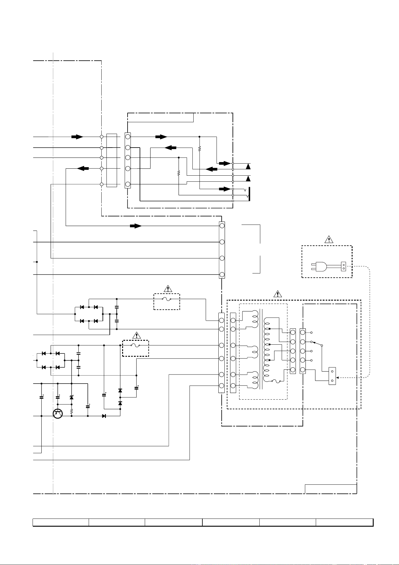
CD-BK110V/CD-BP99V
– 16 –
• The indicated voltage in each section is the one measured
by Digital Multimeter between such a section and the chas-
sis with no signal given.
1. In the tuner section,
indicates AM
indicates FM stereo
2. In the main section, a tape is being played back.
3. In the deck section, a tape is being played back.
( ) indicates the record state.
4. In the power section, a tape is being played back.
5. In the CD section, the CD is stopped.
• Parts marked with “ 1 ” ( ) are important for
maintaining the safety of the set. Be sure to replace these
parts with specified ones for maintaining the safety and
performance of the set.
NOTES ON SCHEMATIC DIAGRAM
• Resistor:
To differentiate the units of resistors, such symbol as K and
M are used: the symbol K means 1000 ohm and the symbol
M means 1000 kohm and the resistor without any symbol is
ohm-type resistor. Besides, the one with “Fusible” is a fuse
type.
• Capacitor:
To indicate the unit of capacitor, a symbol P is used: this
symbol P means pico-farad and the unit of the capacitor
without such a symbol is microfarad. As to electrolytic
capacitor, the expression “capacitance/withstand voltage”
is used.
(CH), (TH), (RH), (UJ): Temperature compensation
(ML): Mylar type
(P.P.): Polypropylene type
• Schematic diagram and Wiring Side of P.W.Board for this
model are subject to change for improvement without prior
notice.
REF. NO
DESCRIPTION
POSITION
SW712 VOLUME UP ON—OFF
SW713 VOLUME DOWN ON—OFF
SW714 CD ON—OFF
SW715 TAPE ON—OFF
SW716 TUNING DOWN ON—OFF
SW717 MEMORY/SET ON—OFF
SW718 REWIND ON—OFF
SW719 FAST FORWARD ON—OFF
SW720 PLAY ON—OFF
SW721 STOP ON—OFF
SW723 REC PAUSE ON—OFF
SW724 TUNING UP ON—OFF
SW725 TUNER BAND ON—OFF
SW801 VOLTAGE SELECTOR 110 V—127 V—
(CD-BK110V ONLY) 220 V—230-240 V
SW1 OPEN/CLOSE ON—OFF
SW2 CLAMP ON—OFF
SW3 DISC NUMBER ON—OFF
SW4 PICKUP IN ON—OFF
SW601 SPAN SELECTOR 50/9 Hz—100/10 Hz
SW701 ON/STAND-BY ON—OFF
SW702 CLOCK ON—OFF
SW703 TIMER ON—OFF
SW704 KARAOKE MODE ON—OFF
SW705 P.B.C. ON—OFF
SW706 OSD ON—OFF
SW707 DIGEST ON—OFF
SW709 DISC SKIP ON—OFF
SW710 OPEN/CLOSE ON—OFF
SW711 EQ./X-BASS/DEMO ON—OFF
TYPES OF TRANSISTOR AND LED
REF. NO DESCRIPTION POSITION
(1) (2) (3)
(S) (G) (D)
E C B
FRONT
VIEW
C B E
FRONT
VIEW
B C E
FRONT
VIEW
2SC1845 F
2SC3331 S
KRC102 M
KRC104 M
KRC107 M
KTA1266 GR
KTA1298 Y
4204SRT7KTC20269014 C
FRONT
VIEW
KTA1271 Y
KTA1273 Y
KTA1504 GR
KTC3194 Y
KTC3203 Y
KTC3265 Y
– 17 –
CD-BK110V/CD-BP99V
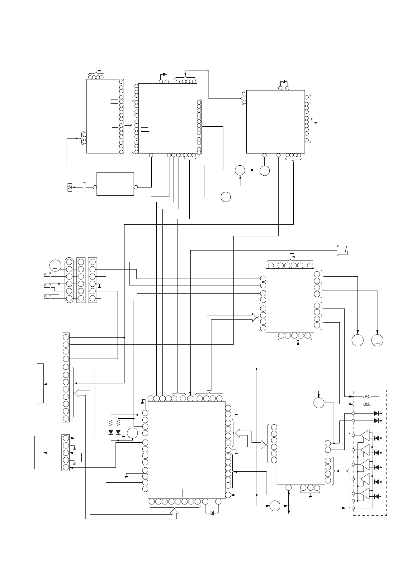
Figure 17 BLOCK DIAGRAM (1/3)
CNP12
CNP11
Q2
+3.3V
+5V
CONT5
CONT2
CONT3
CONT4
CONT7
CONT6
SLDO
SPDO
FDO
TDO
+5V
TO DISPLAY SECTION
CLAMP SW
CDINT
WRQ
CE
DO
CLK
DI
CD RES
GND
SBUSY
MBUSY
DRF
CNS4
BI4
CNP4
M2
SLED
MOTOR
M1
SPINDLE
MOTOR
M
M
TRACKING COIL
FOCUS COIL
PICKUP UNIT
TE
FE
PH(RFENV)
HFL
VVDD
ADAVDD
VDD
LVDD
RVDD
XVDD
VDD5V
FE-
REFV
FE
TE-
TE
HFL
+3.3V
CONSTANT
VOLTAGE
+5V
Q1
Q3
LASER
DRIVER
LDD
PD
VCC3
VCC2
VCC4
VCC1
TIN2
TIN1
FIN2
FIN1
IC3
M63001FP
FOCUS/TRACKING/
SPIN/SLED DRIVER
IC1
LA9235M
SERVO AMP.
TO MAIN SECTION
(TO IC601)
R-CH
L-CH
AGND
DGND
+5V
RCHO
RVSS
LVSS
LCHO
IC2
LC78636E
SERVO/SIGNAL
CONTROL
-
+
M
SW1
OPEN/
CLOSE
XL1
16.9344 MHz
6
5
4
3
3
2
5
4
1
1
2
3
4
7
8
2
1
7
8
9
10
11
12
1
2
4
3
5
SW2
CLAMP
SW3
DISC
NUMBER
M3
T/T
UP/DOWN
LOADING
MOTOR
6
1
2
4
3
5
6
1
2
4
3
5
6
75
76
45
53
46
47
48
32
31
30
40
65 66
67
68
69
70 71 72
CE
CL
DI
DO
INT
WRQ
RES
DEF
52
51
XOUT
XIN
73
5
18
36
44
49
50
7
3
14
15
16
19
23
242526
3359
5735545556
17
18
19
20
21
22
30 23 11 9
1
4
5
6
7
15
16
26
27
2
17
25
41
42
38
39
35 29 22 21 14 8
40
18
24 23 28
SW4
PICKUP IN
+3.3V
QV3
+3.3V
XV1
4.19 MHz
7
XV2
27 MHz
ICV1
MPEG CONTROLLER
IX0495AW
ICV2
D61012GC
MPEG DECODER
ICV3
SDM4260C
DRAM
~~
~
~
~~
~
~
~~
~
~~
~~~
~
~
~~
~~
~
MBUSY
MCK
MDO
MDI
X1
X2
PWR_MPEG
SBUSY
ICV4
NJM2267M
VIDEO
OPERATION AMP.
CNPV3
JK902
VIDO OUT
JACK
HD7
HD0
AUDO
AUBCK
AULRCK
CDC2PO
CDLRCK
CDBCK
CDI
X1
X2
VOUT1
VDD,CKSEL,HSELX,
HSELA,AVDD
HD7
HD4
HD3
HD0
MA8
MA4
MA3
MA0
MRAS
MWE
MCAS
MD5
MD7
MD4
MD0
MD11
MD8
~
~~
MD15
MD12
VDD
DQ0
DQ3
DQ4
DQ7
DQ8
DQ11
DQ12
DQ15
WE
RAS
A0
A3
A4
A8
9
14
16
22
20
1918
40
64
1
15
17
23
25
36
44
51
63
75
83
84
92
257
1014
38
2
1
6
20
5
7
86
16
35 32 339597 98 99
42
45
10
13
14
16
19
22
26
31
34
36
39
21273540
~
~~
~~
48
49
52
53
54
56
58
62
65
68
70
73
13
57
41
15 44
17
25
33
42
45
50
~
~
QV2
~
29
28
LCAS
UCAS
QV4
~~
+B
VCC
+B
+B
13
64
+B
CD-BK110V/CD-BP99V
– 18 –
Figure 18 BLOCK DIAGRAM (2/3)
AM LOOP
ANTENNA
SO302
FM ANTENNA
TERMINAL
FM
ANTENNA
CNP302
1
2
L
R
5
4
+B4
Q102
Q103
IC101
AN7345K
RECORD/
PLAYBACK AMP.
VF2
+5
V
UN
_
FM+B
+B3
CL
+B5
AM IF
OSC BUFF
FM IF
FM
OSC
B.P.F
CNS601
Q107-
Q104
Q110
Q111
Q601
Q602
10.7 MHz
450kHz
REC/PLAY
CLK
CE
DI
DO
DI
CE
MO/ST
CONSTANT
VOLTAGE
+B3
+B2
+B2
FM/AM
IC302
LC72131
PLL(TUNER)
FM/AM
OUT
L
R
BIAS
T1/T2
MUTING
P.B.
REC.
AC BIAS
L
R
L
R
L
R
L
R
TAPE
TUNER
CD
P.B.
CNP11
FROM VIDEO
CD SECTION
ERASE
HEAD
SWITCHING
SWITCHING
BIAS
Q101
Q113
Q706
SWITCHING
Q114
BIAS
OSC
Q112
L103
Q104
Q106
RECORD/
PLAYBACK
HEAD
TAPE 2
PLAYBACK
HEAD
TAPE 1
L-CH
R-CH
L-CH
R-CH
IC601
LC75341
AUDIO PROCESSOR
+B3
REC.
R
L
L NF
R NF
R REC
L REC
R NF
L NF
SWITCHING
L(T2)
R(T2)
R(T1)
L(T1)
R
L
FM/AM
MPX
IN
STEREO
AM RF IN
AM OSC IN
FM
Q360
VT
X IN X OUT
X352
4.5 MHZ
AM BAND
COVERAGE
AM TRACKING
T303 T306
Q302
X351
456 kHz
MO/ST
MPX
VCO
FM
DET
VCC
GND
AM IF
CF351
IC303
LA1832S
FM IF DET/.
FM MPX./
AM IF
AM MIX
CF352
T351
RF
FM
OSC
FM
L312 T301
CF302T302
IC301
TA7358AP
FM FRONT END
BF301
21
22
3
4
24
2
1
178
3
9
10
18
11
3
15
10
23
14
12
13
1
2
19
7
18
8
17
44
42 43
50
51
13
21
4
2
24
23
9
16
15
13
12
1
5413
83
1
21
7
98517
6
21
21
20 22 11
17
1615
9
6
5
7
13
14
12
15
1623
4
7
H/N
P.B
REC
T1/T2
VR401
MIC
VOLUME
SYSTEM
MUTE
VDD
Q401
Q402
Q403~
Q406
JK1
MIC
SWITCHING
IC701
IX0338AW(2/2)
MOTOR
DRIVER
SOLENOID
DRIVER
TAPE
MECHANISM
ASS'Y
Q704
Q705
BUFFER
TAPE 2
SWITCHING
L R
– 19 –
CD-BK110V/CD-BP99V
Figure 19 BLOCK DIAGRAM (3/3)
SW601
SPAN
SELECTOR
53
3
1
2
KIA7810AP
VOLTAGE REGULATOR
–VP
VF1
VF2
Q904
Q905
+5V(CD_+B)
+B4
UN_SW_5V
+B5
KIA7805AP
VOLTAGE
REGULATOR
IC904
+B3
M+10V
+B2
+B1
+B6
-
10
30
–
R
L
+B5
+B5
RX701
LED722
REMOTE
SENSOR
D911~D914
D907~D910
JK901
HEADPHONES
Q707
Q701
IC902
IC901
LA4282
POWER AMP.
A+10V
F902
T1.6A L 250V
F901
T2.5A L 250V
Vcc
R-OUT
L-OUT
CLK
SO901
SPEAKER
TERMINAL
VLOAD
RESET
+B5
+B5
+B5
+B5
+B5
+B5
+B6
VDD
VDD
VDD
–
CE
DI
DO
XL701
4.1943 MHz
–
A
S
T
2
AVDD
AVD1
SW701-SW707
SW709-SW721
SW723-SW725
KEY
TO CD
SECTION
IC701
IX0338AW(1/2)
SYSTEM
MICROCOMPUTER
FL701
FL DISPLAY
333231
71
11
99
80
1
4
56 78
5
2
312
3
1
2
9
4
11
10
7
78
33
31
4546
1112
9
1 0 16 1 7 20 2123
60
2224
79
100
40
39
35
34
T.F.
PT801
POWER
TRANSFORMER
110 V
127 V
220 V
230-240 V
SW801
VOLTAGE
SELECTOR
AC POWER
SUPPLY CORD
AC 110/127/220/230-240 V
50/60 Hz
SO902
AC INPUT SOCKET
AC 110/127/220/230-240 V
50/60 Hz
RESET
CD-BK110V
CD-BK110V
R
L
IC901
BA5415A
POWER AMP.
Vcc
R-OUT
L-OUT
8
5
12
2
1
11
CD-BP99V
T.F.
PT801
POWER
TRANSFORMER
AC POWER
SUPPLY CORD
AC 220-240 V
50/60 Hz
SO902
AC INPUT SOCKET
AC 220-240 V
50/60 Hz
CD-BP99V
+B1
IC704
KIA7042A
SYSTEM
RESET
-
-
CONSTANT
VOLTAGE
GND
GND
15
CD-BK110V/CD-BP99V
– 20 –
Figure 20 SCHEMATIC DIAGRAM (1/14)
A
B
C
D
E
F
G
H
1
23456
• NOTES ON SCHEMATIC DIAGRAM can be found on page 16.
LUG1
TAPE
MECHANISM
R-CH
L-CH
TAPE 2
ERASE HEAD
R-CH
L-CH
TAPE 2
RECORD/PLAYBACK
HEAD
TAPE 1
PLAYBACK HEAD
5
4
3
2
1
5
4
3
2
1
A_GND
L-CH
CD_GND
+5V
GND(A_GND)
R-CH
L
R
+5V
GND(CD_GND)
Q601.Q602:SYSTEM MUTE
7
6
5
4
3
2
1
7
6
5
4
3
2
1
3
2
1
3
2
1
TAPE1_R
A_GND
TAPE1_L
SWITCHING
SWITCHING
GND
KT-R
KCD-L
KT-L
12345678
1718192021222324
R
L
MU
T
1
2
3
1
2
3
GND
K
19
18
17
16
15
14
13
L4
L3
L2
LSELO
L1
R1
R2
R3
R4
RSELO
RIN
RTRE
AUX
DECK
TUN
CD
AUX
DECK
TUN
CD
7
6
5
4
3
INTERFACE
+
––
+
–
+
–
–
+
–
+
VSS
LOUT
LBASS
LTRE
LIN
RBASS
+
–
+
–
12
11
10
9
8
2
1
24
23
22
21
20
+
DI
CE
ROUT
VREF
VDD
CLK
CCB
+B
+B
SWITCHING
SWITCHING
15
19
17
18
16
P24 1 - F,G (CD-BK110V)
P26 1 - F,G (CD-BP99V)
TO POWER SECTION
P33 12 - D
TO VIDEO CD PWB
CD-BK110V
ONLY
CNP11
SWITCHING
SWITCHING
SWITCHING
Q403-406:
SWITCHING
R127
6.8K
C129
R131
C119
0.033
(ML)
C121
560P
C113
330P
C123
1/50
C117
100/16
R117
56
R123
5.6K
R125
12K
C147
0.001
R129
3.9K
C127
270P
C137
0.022
C139
3.3/50
C112
330P
C114
330P
C118
0.033
(ML)
C120
560P
R114
1K
R118
100K
R120
3.9K
C116
100/16
C122
1/50
R116
56
R122
5.6K
C128
C126
270P
C146
0.001
R128
6.8K
R130
3.9K
R126
68K
R124
12K
R134
100
R132
R137
15K
R138
15K
R121
3.9K
R119
100K
R115
1K
C115
330P
C104
180P
Q106
2SC1845 F
Q104
2SC1845 F
R106
2.2K
R108
3.3K
C105
180P
Q107
2SC1845 F
Q105
2SC1845 F
R109
3.3K
R107
2.2K
Q109
2SC3331 S
R111
4.7K
R113
47K
Q108
2SC3331 S
R110
47K
R112
4.7K
R105
1K
R104
1K
Q406
9014 C
R416
330
R428
10K
Q102
KRC104 M
Q103
KRC104 M
R103
4.7K
C108
100/16
Q101
KTA1266 GR
C101
0.047
R101
10K
R102
10K
C106
560P
C107
560P
R424
4.7K
R420
470K
Q405
9014 C
R415
330
R427
10K
R423
4.7K
R419 470K
C413
1/50
R414
330
R426
10K
R422
4.7K
R418
470K
C433
1/50
Q403
9014 C
Q404
9014 C
R412
330
R410
10K
R421
4.7K
R417
470K
C409
1/50
R429
22K
R433
2.2K
C440
1/50
C414
220/6.3
C412
1/50
Q407
9014 C
R434
470K
R430
22K
Q408
9014 C
R435
4.7K
R439
330
R438
4.7K
R411
210
R432
1K
R437
2.2K
R436
470K
R425
330
C441
1/50
C411
220/6.3
C611
0.1(ML)
C613
0.0027(ML)
C617
1/50
C629
1/50
C623
1/50
C625
1/50
C609
0.1(ML)
C627
1/50
C420
1/50
R617
R431
1K
C615
220P
C616
220P
R615
3.9K
C607
C604
100/25
C605
0.022
C102
560P
C103
560P
C407
4.7/50
C401
1/50
CNP102 CNP101
R405
100K
VR401
50K(A)
C406
1/50
C408
220/6.3
Q402
9014 C
R401
1.5K
R402
1K
R403
470K
Q401
9014 C
C404
1/50
R407
4.7K
R408
560
R404
1M
C403
220P
C402
1/50
C405
0.0047
R409
10K
BI601
CNS601
R601
330
R602
330 R610
R609
Q601
2SC3331 S
Q602
2SC3331 S
R603
1.8K
R604
1.8K
R608
2.2K
R607
2.2K
C602
0.001
C601
0.001
C
4
1
/
C
1
C
1
C
1
0
C
6
2
2
IC601
LC75341
AUDIO PROCESSOR
IC101
AN7345K
IC101
AN7345K
RECORD/PLAYBACK AMP.
JK1
MIC
10/50
R609, R610: 10K (CD-BK110V)
R609, R610: 39K (CD-BP99V)
MIC
VOLUME
C150
0.0033
R617: 3.3K (CD-BK110V)
R617: 2.7K (CD-BP99V)
FM SIGNAL
PLAYBACK SIGNAL
RECORD SIGNAL
CD SIGNAL
MIC SIGNAL
– 21 –
CD-BK110V/CD-BP99V
Figure 21 SCHEMATIC DIAGRAM (2/14)
7
8 9 10 11 12
456789
10 11 12
1314151617181920
2
1
RIPPLE
VCC
GNDALC
MUTING
MUTING
D
REC_R
REC_L
KCD-R
19
18
17
16
15
14
13
R1
R2
R3
R4
RSELO
RIN
RTRE
AUX
DECK
TUN
CD
E
+
–
–
+
–
RBASS
+
–
+
–
24
23
22
21
20
+
ROUT
VREF
VDD
CLK
A_10V
A_10V
SWITCHING
BIAS OSC
BIAS
2 3
1
A_10V
A_10V
GND
1 3 4 5 6 7 9 2
11 12
A_10V
VF1
–VP
VF2
M_10V
SW_5V
UN_SW_5V
POWER
GND(M_GND)
P24 1 - G,H (CD-BK110V)
P26 1 - G,H (CD-BP99V)
TO POWER SECTION
GND(D_GND)
21
20
19
18
17
16
15
14
13
12
11
10
9
8
7
6
5
4
3
2
1
P29 12 - C
TO DISPLAY PWB
CE
DO
DI
CLK
T_BIAS
T_T1/T2
REC/PLAY
M_GND
M_10V
SMUTE
VF1
–VP
VF2
UN_SW 5V
D_GND
SW 5V
+B
+B
+B
+B
+B
+B
+B
+B
+B
+B
POWER
SPAN
SW OUT
28
27
26
25
24
23
22
21
20
P23 11,12 - H
TO TUNER SECTION
A_10V
CE
DI
CLK
TUN_R
GND(D_GND)
GND(A_GND)
DO
TUN_L
50/9 kHz
100/10 kHz
MAIN PWB-A (1/3)
MIC PWB-C
(CD-BK110V ONLY)
SOK2
21
1
SW601
SPAN
SELECTOR
R127
6.8K
C135
47/50
C129
22/50
R133
100
C131
0.022
R131
C133
0.0033
R135
10K
C121
560P
C123
1/50
R123
5.6K
2
5
K
C147
0.001
R129
3.9K
C127
270P
C137
0.022
C139
3.3/50
1
8
3
3
L
)
C120
560P
1
8
0
K
R120
3.9K
C122
1/50
R
122
5
.6K
C136
22/50
C134
47/50
C128
22/50
C126
270P
C146
0.001
C132
0.0033
R136
10K
R128
6.8K
R130
3.9K
R126
68K
C130
0.022
R134
100
R132
Q110
2SC3331 S
D101
1N4148
R140
10K
R141
10K
D102
1N4148
Q111
2SC3331 S
R150
1K
R142
220K
C138
220/6.3
C145
0.001
C140
0.0082(P.P.)
C141
0.039(ML)
C148
0.047
R148
22K
R149
4.7
R147
47K
R146
82
Q114
KTC3203 Y
C142
47/50
Q112
KTA1266 GR
Q113
KRC104 M
R144
47K
R145
4.7K
C109
0.001
L103
100µH
D103
1N4148
C110
10/50
R143
220K
R121
3.9K
100K
R151
1K
1
08
0
/16
R157
100
R432
1K
4
1
5
0
R625
22K
C603
1/50
CNP701
L104
330µH
R139
180
R618
C421
1/50
C628
1/50
C626
1/50
C624
1/50
C619
220P
R616
3.9K
C610
0.1(ML)
C612
0.1(ML)
C614
0.0027(ML)
C618
1/50
C630
1/50
C608
10/50
C606
22/50
IC101
AN7345K
FFC701
R131: 1.2K (CD-BK110V)
R131: 1.5K (CD-BP99V)
R132: 1.2K (CD-BK110V)
R132: 1.5K (CD-BP99V)
R618: 3.3K (CD-BK110V)
R618: 2.7K (CD-BP99V)
CD-BK110V/CD-BP99V
– 22 –
A
B
C
D
E
F
G
H
1
23456
• NOTES ON SCHEMATIC DIAGRAM can be found on page 16.
Figure 22 SCHEMATIC DIAGRAM (3/14)
5
6
7
8
9
1234
TP301
AM TRACKING fL
RF BY PASS
RF IN
RF OUT
MIX IN
GND
MIX OUT
OSC MONI
OSC
VCC
1
2
1
2
AM LOOP
ANTENNA
FM IF
FM OSC.
AM BAND
COVERAGE fL
FM RF
13
2
BUFFER
MAIN PWB-A (2/3)
+B
+B
D301
1SS133
D302
1SS133
C323
0.022
T303
C330
15P
C332
0.022
VD301
SVC348S
C331
0.047
R336
10K
R323
68K
C334
27P
T306
AM OSC.
IC301
TA7358AP
FM FRONT END
C303
10P
BF301
C304A
100P
C304
0.001
C305
5P
C321
0.001
SO302
FM ANTENNA
TERMINAL
C308
5P
D305
1SS133
L312
C309
0.001
R311
100K
VD302
SVC211C
R313
R314
22
C315
0.0047
C314
0.0047
C316
0.001
C317
0.001
R322
680
R325
47K
Q302
KTC3194 Y
R327
33
C302
0.001
C301
0.001
D304A
1SS133
D303A
1SS133
C318
100P
T302
C312
0.022
T301
C324
4P
R309
10K
C313
22P
VD303
SVC211C
R316
4.7K
CF302
R382
150
C397
0.022
C320
0.022
C322
0.001
C381
12P
X352
4.5 MHz
C382
15P
R375
820
C35
1
0.02
2
C342
0.022
R358
3.9K
CNP302
R302
22
C306
0.022
C307
10/50
C311
18P
C310
15P
C335
560P
33K
AM ANTENNA
13
2
D304
1SS133
D303
1SS133
B.P.F.
FM SIGNAL
AM SIGNAL
– 23 –
CD-BK110V/CD-BP99V
Figure 23 SCHEMATIC DIAGRAM (4/14)
7
8 9 10 11 12
5
6
7
8
9101112
131415161718192021222324
1234
5
6
7
8
91011
1213141516171819202122
1234
T
P301
TP302
L-CH
OUT
R-CH
OUT
MPX
IN
MPX
VCO
AM
RF IN
FM
AFC
AM OSC
IN
AM OSC
OUT
FM IF
IN
AM MIX
OUT
REG
AM IF
IN
GND
VSM
AM LOW
CUT
FM/AM
OUT
FM/AMPHASE
AM IF
A_10V
A_GND
UN_SW_5V
SW_5V
TUN_R
TUN_L
DI
CE
DO
CLK
GND
(D_GND)
P21 12 - C
TO MAIN SECTION
P24 1 - G (CD-BK110V)
P26 1 - G (CD-BP99V)
TO POWER SECTION
X OUT
VSS
AOUT
AIN
PO
VDD
FM IN
AM IN
N.C
IF IN
SD
X IN
N.C
CE
DI
FM/AM
IF
CONT
FM/AM
DO
CL
ST INO
MO/ST
SD FM DET
IF
OUT
VCC
MO/ST
STEREO
13
2
CONSTANT
VOLTAGE
20 287 9 24 25 22 21 26 23 27
+B
+B
+B
+B
+B
R382
150
C397
0.022
C394
47/16
C392
0.001
R381
10K
R380
1.5K
C393
1/50
C380
10/50
C387
0.022
R379
2.2K
C385
0.01
L351
100µH
C386
330P
IC302
LC72131
PLL (TUNER)
R395
47K
R360
4.7K
C320
0.022
C322
0.001
C381
12P
X352
4.5 MHz
C382
15P
R375
820
C319
100P
R374
1K
R373
1K
R372
1K
R378
1K
R386
22K
R376
1K
C391
47/16
R384
5.6K
R383
5.6K
R385
5.6K
Q360
KTA1266 GR
R359
1.8K
R387
5.6K
R377
47K
R393
1K
C351
0.022
C352
10/50
C350
0.022
T351
CF352
R352
1K
C353
0.022
C354
0.022
R353
390
C398
100/16
C357
2.2/50
R355
3.3K
C356
0.001
CF351
C399
0.022
C355
22P
R388
3.9K
C370
1/50
L352
100µH
D306
1SS133
C396
100/16
C395
0.022
R351
5.6K
R365
10K
C342
0.022
R358
3.9K
C362
3.3/50
C361
0.022
C364
10/50
C363
0.022
C365
0.022
X351
456 kHz
C366
0.001
C367
1/50
R350
2.7K
R357
470K
R356
1K
C368
1/50
C369
27P
C374
0.015(ML)
C373
0.015
(ML)
C371
1/50
R361
C372
1/50
R362
R364
6.8K
R363
6.8K
IC303
LA1832S
FM IF DET./
FM MPX./AM IF
C358
1/50
R361, R362: 5.1K (CD-BK110V)
R361, R362: 3.3K (CD-BP99V)
CD-BK110V/CD-BP99V
– 24 –
Figure 24 SCHEMATIC DIAGRAM (5/14)
A
B
C
D
E
F
G
H
1
23456
• NOTES ON SCHEMATIC DIAGRAM can be found on page 16.
234
5
6
7
8
9101112
1
16
15
17
9
4
5
6
11
18
19
1
2
3
12
P20 1 - C/P23 10 - H/P21 10 - H
TO MAIN SECTION/TUNER SECTION
GND(A_GND)
L
R
POWER
GND(CD_GND)
A_10V
SW_5V
UN_SW_5V
VF1
–VP
VF2
M_10V
GND(D_GND)
GND(M_GND)
+5V(CD_+B)
7
1
3
2
MUTE
RIPPLE
FILTER
PRE-GND
IN2
POWER
GND2
VCC
OUT1
POWER
GND1
CH2
+
NF2
OUT2
–
THERMAL OVER
VOL. PROTECTOR
CH1
+
–
1
1
2
2
33
1
3
+B
+B
+B
+B
+B
+B
+B
+B
+B
2
IC901
LA4282
POWER AMP.
C905
0.022
C906
100/16
C907
100/25
R905
120
R907
1K
C909
0.082(ML)
C918
220P
R906
1K
C908
0.082(ML)
R908
120
C914
1000/25
C910
100/25
R910
270
R909
56K
C911
0.022
C919
10/50
C915
1000/25
C912
0.1(ML)
C916
0.1(ML)
R912
4.7
R911
270
R913
4.7
C917
0.1(ML)
C913
0.1(ML)
C903
470P
C904
470P
Q901
KRC102 M
R914
22K
Q902
KRC102 M
C946
2200/50
R915
820
C933
68P
C934
0.047
(ML)
R922
22K
C935
22/50
D922
DZ3.9BSB
Q905
KTC2026
R923
560
IC902
KIA7810AP
C940
0.1(ML)
C939
0.1(ML)
C938
47/50
R925
22K
IC904
KIA7805AP
C945
0.1(ML)
D918
1SS133
C944
0.022
C943
47/50
R926
10K
D902
1N4001
C947
3300/35
R928
12K
C954
100/50
C955
47/50
C956
47/50
R927
2.2K
Q904
KTA1266 GR
ZD903
MTZJ6.2A
R930
220
R929
220
D913
D914
D911 D912
IC902, IC904: VOLTAGE REGULATOR
D911~D914: 1N4004S
CONSTANT
VOLTAGE
FM SIGNAL
CD-BK110V
– 25 –
CD-BK110V/CD-BP99V
Figure 25 SCHEMATIC DIAGRAM (6/14)
7
8 9 10 11 12
AC POWER
SUPPLY CORD
AC 110/127/220/230-240 V
50/60 Hz
6
5
4
3
5
4
3
2
1
5
4
3
2
1
2
1
6
5
4
3
2
1
220V
230-240V
110V
127V
–
+
–
+
1
5
4
3
2
1
5
SP_R-CH_GND
SP_R-CH
SP_L-CH_GND
SP_L-CH
B
+B
HEADPHONES PWB-D
MAIN PWB-A(3/3)
PW901A
PW901B
R916
220
JK901
HEADPHONES
SO902
AC INPUT SOCKET
CNP801
CNS801
T.F.
CNP901
CNS901
F901
T2.5A L 250V
C950
0.047(ML)
C951
0.047(ML)
D909 D910
D907 D908
0
C955
47/50
C956
47/50
ZD902
DZ30BSB
C957
47/50
R927
2.2K
Q904
KTA1266 GR
D917
1N4004S
C958
100/50
D915
1N4004S
D916
1N4004S
C959
100/50
0
3
6
.2A
D913
D914
D911 D912
C953
0.047(ML)
C952
0.047(ML)
F902
T1.6A L 250V
R917
220
AC 110/127/220/230-240 V
50/60 Hz
4
S
D907~D910: 1N4004S
PT801
POWER TRANSFORMER
SW801
VOLTAGE
SELECTOR
SO901
SPEAKER
TERMINAL
CD-BK110V/CD-BP99V
– 26 –
Figure 26 SCHEMATIC DIAGRAM (7/14)
A
B
C
D
E
F
G
H
1
23456
• NOTES ON SCHEMATIC DIAGRAM can be found on page 16.
234
5
6
7
8
9101112
1
16
15
17
9
4
5
6
11
18
19
1
2
3
12
P20 1 - C/P23 10 - H/P21 10 - H
TO MAIN SECTION/TUNER SECTION
GND(A_GND)
L
R
POWER
GND(CD_GND)
A_10V
SW_5V
UN_SW_5V
VF1
–VP
VF2
M_10V
GND(D_GND)
GND(M_GND)
+5V(CD_+B)
+B
+B
+B
+B
+B
+B
+B
7
1
3
2
1
3
2
VCC GND
IC901
BA5415A
POWER AMP.
C903
470P
C904
470P
C946
3300/35
C933
68P
C934
0.047
(ML)
R922
22K
C935
22/50
D922
DZ3.9BSB
Q905
KTC2026
R923
33
IC902
KIA7810AP
C940
0.1(ML)
C939
0.1(ML)
C938
47/50
R925
22K
IC904
KIA7805AP
C945
0.1(ML)
D918
1SS133
C944
0.022
C943
47/50
R926
10K
D902
1N4001
C947
3300/35
R928
12K
C954
100/50
C955
47/50
C956
47/50
R927
2.2K
Q904
KTA1266 GR
ZD903
MTZJ6.2A
R930
220
R929
220
D913
D914
D911 D912
IC902, IC904: VOLTAGE REGULATOR
D911~D914: 1N4004S
R902
1.8K
R901
1.8K
C901
0.1(ML)
C906
0.1(ML)
C902
47/16
R904
240
R903
240
C914
100/16
C912
100/16
C911
100/16
C907
47/16
C908
1000/25
C905
1000/25
C916
4.7/50
R910
4.7K
D901
1N4148
CONSTANT
VOLTAGE
R931
1K
FM SIGNAL
CD-BP99V
– 27 –
CD-BK110V/CD-BP99V
Figure 27 SCHEMATIC DIAGRAM (8/14)
7
8 9 10 11 12
+B
6
5
4
3
2
1
2
1
2
1
6
5
4
3
2
1
–
+
–
+
1
5
4
3
2
1
5
SP_R-CH_GND
SP_R-CH
SP_L-CH_GND
SP_L-CH
HEADPHONES PWB-D
MAIN PWB-A(3/3)
PW901A
PW901B
R916
68
JK901
HEADPHONES
SO902
AC INPUT SOCKET
AC 220-240 V
50/60 Hz
CNP801
CNS801
T.F.
CNP901
CNS901
F901
T2.5A L 250V
C950
0.047(ML)
C951
0.047(ML)
D909 D910
D907 D908
0
C955
47/50
C956
47/50
ZD902
DZ30BSB
C957
47/50
R927
2.2K
Q904
KTA1266 GR
D917
1N4004S
C958
100/50
D915
1N4004S
D916
1N4004S
C959
100/50
0
3
6
.2A
D913
D914
D911 D912
C953
0.047(ML)
C952
0.047(ML)
F902
T1.6A L 250V
R917
68
4
S
D907~D910: 1N4004S
PT801
POWER TRANSFORMER
SO901
SPEAKER
TERMINAL
AC POWER
SUPPLY CORD
AC 220-240 V
50/60 Hz
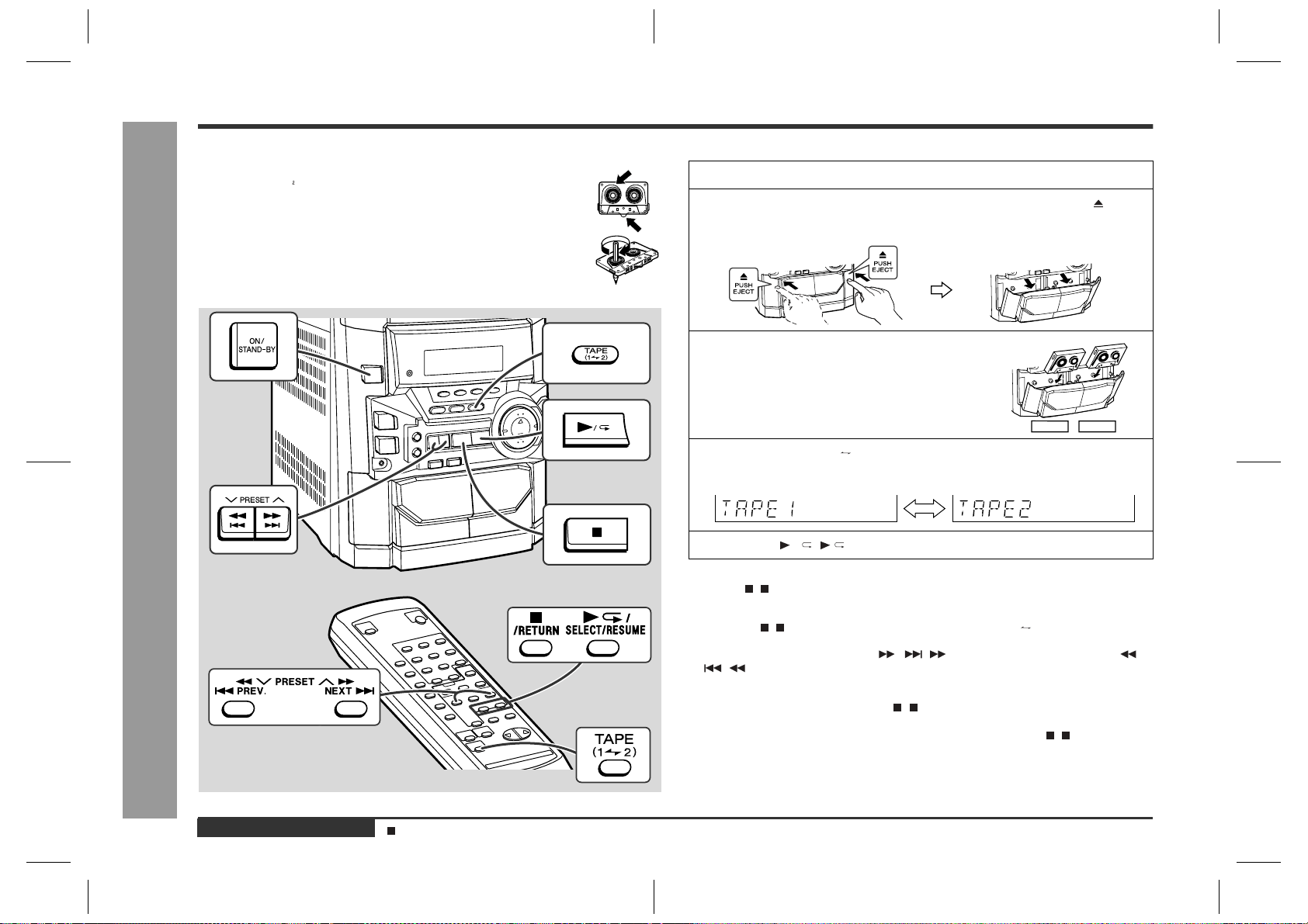
CD-BK110V/CD-BP99V
– 28 –
A
B
C
D
E
F
G
H
1
23456
• NOTES ON SCHEMATIC DIAGRAM can be found on page 16.
Figure 28 SCHEMATIC DIAGRAM (9/14)
10V
0V
10V
0V
10V
10V
10V
10V
0V
–
4.9V
TAPE MECHANISM
PWB-F
M
11
10
9
8
7
6
5
4
3
2
1
11
10
9
8
7
6
5
4
3
2
1
SOLENOID
SOLENOID
+
–
TAPE
MOTOR
PLAY SW1
END SW1
F_REC
SOL1
SOL2
MTR+
END SW2
GND
PLAY SW2
T2 PLAY
GND
T2 RUN
+MTR
SOL2
SOL1
F_REC
T1 RUN
T1 PLAY
1 2 3 4 5 6 7 8 9
10 11 12 13 14 15 16 17 18 19 20 21 22 23 24 25 26 27 28 29 30 31 32 33
F1
F2
P15
P16
P13
P20
P14
P11
P10
P9
P8
P7
P6
5G
P5
P4
6G
7G
P3
P2
8G
P1
P12
P19
P18
P17
2G
1G
4G
3G
9G
F4
F3
80
80
79
78
77
76
75
74
73
72
71
70
69
68
67
66
65
64
63
62
61
60
59
58
57
56
55
54
53
52
51
54
53
52
51
30
29
30
29
28
27
26
25
24
23
22
21
20
19
18
17
16
15
14
13
12
11
10
9
8
7
6
5
4
3
2
1
1
50
49 48 47 46 45 44 43 42 41 40
39 38 37 36 35 34 33 32 31
81 82 83 84 85 86 87 88 89 90 91 92 93 94 95 96 97 98 99
100
KEY3
SPEANA0
SMUTE
VSS
REMOCON
NO USE
SP_PLA
SYS STOP
AVD1
KEY0
AVDD
KEY2
SPEANA2
SPEANA3
M+BUSY/TUN SM
VDD
TIMER LED
T_MOTOR
T_SOL_A
T_SOL_B
T1 RUN
SPK_DET
PLAY_CONT
POWER
T2 RUN
CD CLAMP SW
T1 PLAY SW_A
T2 PLAY SW_B
FPA
FPB
KARAOKE LATCH
MIC IN
DISTOUT/SW OUT
SPN
N.C.
DIST3
DIST2
DIST1
DIST0
P15
P16
P13
P20
P14
P11
P8
VLOAD
P9
P10
P7
P6
P5
P4
P3
P2
P1
P12
P19
P18
P17
5G
6G
7G
8G
1G
2G
3G
4G
9G
VDD
–20DB ATT
S_BUSY
T_BIAS
T_T1/T2
REC/PLAY
RES OUT
DRF
WRQ
RESET
X2
X1
VPP/IC
XT2
CD INT
VDD
CD CLK
CD DI
CD DO
CD CE
CE
CLK
DI
DO
AVSS
N.C.
N.C.
N.C.
N.C.
N.C.
SPEANA1
+B
+B
AC
1
2
1
11
MOTOR DRIVER
+B
+B
SOLENOID
DRIVER
O
Q705
KTA1271 Y
Q706
KTA1273 Y
R768
10K
Q704
KTA1271 Y
D703
1SS133
D702
1SS133
C710
47/16
R767
10K
R766
10K
SOK3
R719
1K
R720
1K
R721
1K
R722
10K
R724
1K
R726
2.2K
R727
2.2K
R728 2.2K
R729 2.2K
R778 1K
R792 1K
R732 1K
R737 1K
R736 1K
R735 1K
R734 1K
R742
1K
D714
1SS133
R750 10K
R749
10K
R751 10K
R748
4.7K
R753 10K
R777
10K
R755
4.7K
R775
10K
R776
10K
R758
10K
R759
10K
R702
R703
R704
R705
R706
R707
R708
R
R710
R717
R716
R715
R714
R713
R712
R711
Q7
0
KRC1
0
R744
1K
LED722
4204SRT7
D701
1SS133
R733
1K
C705 100/10
C708 1/50
R743 33
FL701
FL DISPLAY
IC701
IX0338AW
SYSTEM
MICROCOMPUTER
FFC702
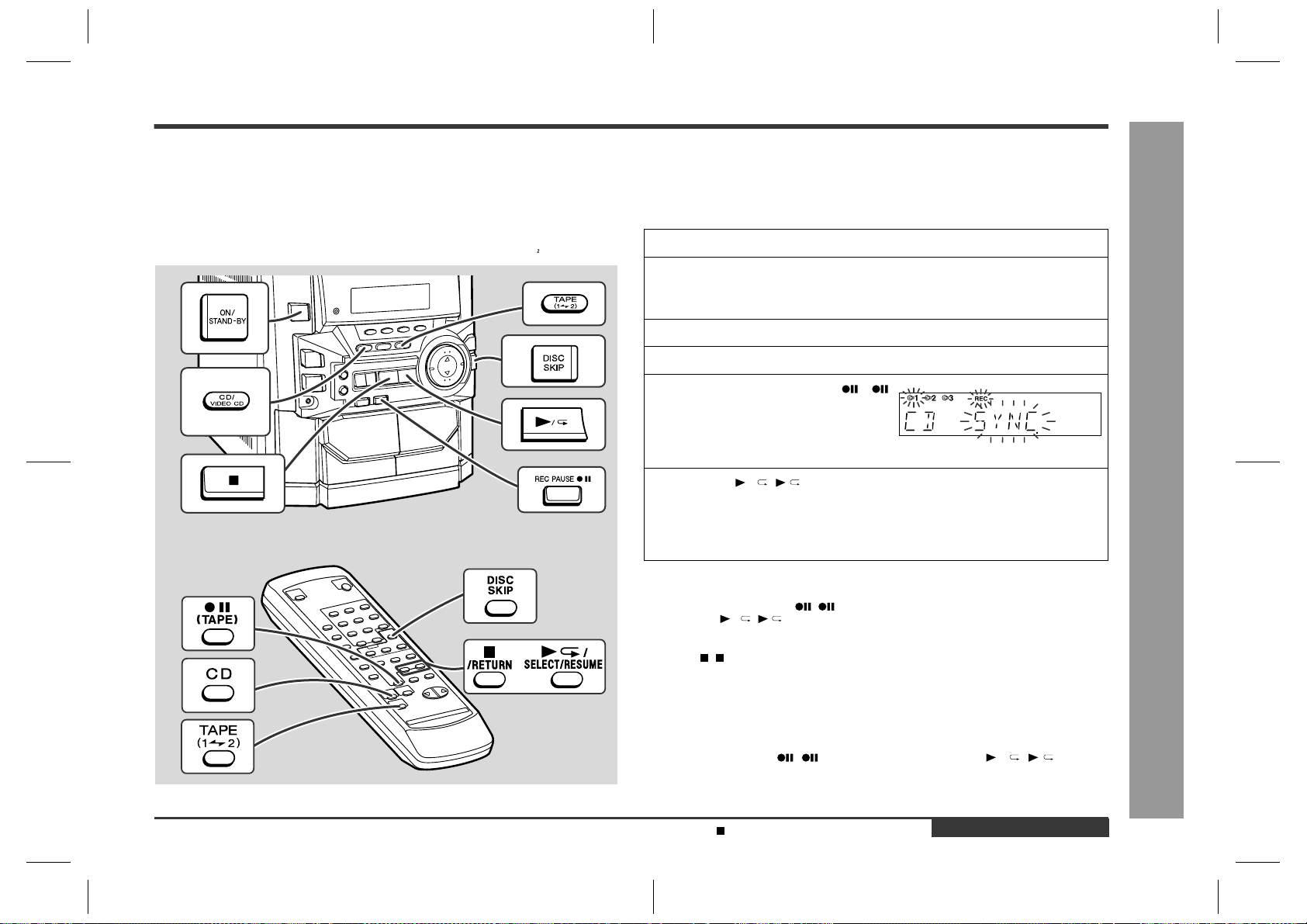
– 29 –
CD-BK110V/CD-BP99V
Figure 29 SCHEMATIC DIAGRAM (10/14)
7
8 9 10 11 12
–25.6V
–25.4V
4.9V
9.7V
0V
0V
3
0 31 32 33
4G
9G
F4
F3
30
29
28
27
26
25
24
23
22
21
20
19
18
17
16
15
14
13
12
11
10
9
8
7
6
5
4
3
2
1
34 33 32 31
97 98 99
100
KEY3
KEY0
AVDD
KEY2
SPEANA2
SPEANA3
B
USY/TUN SM
2G
3G
4G
9G
–20DB ATT
S_BUSY
T_BIAS
T_T1/T2
REC/PLAY
RES OUT
DRF
WRQ
RESET
X2
X1
VPP/IC
XT2
CD INT
VDD
CD CLK
CD DI
CD DO
CD CE
CE
CLK
DI
DO
AVSS
1
2
3
2
1
3
1
+B
2
3
213
3 2
1
10
11
12
9
8
7
6
5
4
3
2
1
10
11
9
8
7
6
5
4
3
2
1
21
20
19
18
17
16
15
14
13
12
11
10
9
8
7
6
5
4
3
2
1
P33 12 - F
TO VIDEO CD PWB
CD INT
DRF
WRO(DSP)
CD CE
CD DO
CD DI
CD CLK
RES OUT
CLAMP SW
CD GND
SBUSY
MBUSY
TUN SM
CE
DO
CLK
T-BIAS
T_T1/T2
REC/PLAY
M_GND
M_10V
SMUTE
VF1
–VP
VF2
AC_RLY CONT
UN_SW 5V
D_GND
SW_5V
POWER
SPAN
SW OUT
CNP12
DI
CNP701
P21 12 - E
TO MAIN PWB
1
21
DISPLAY PWB-B
+B
+B
+B
+B
+B
+
B
+B
+B
12
SW701
ON/STAND-BY
RD01
680
SW702
CLOCK
RD02
820
SW703
TIMER/SLEEP
RD03
1K
RD04
1.5K
RD05
2.2K
RD06
2.7K
RD07
3.9K
SW709
DISC SKIP
SW710
OPEN/CLOSE
RD08
56K
RD26
6.8K
RD09
100K
SW714
CD
RD13
680
SW715
TAPE
RD14
820
SW716
TUNING
DOWN
RD15
1K
SW717
MEMORY/SET
RD16
1.5K
SW718
REWIND
RD17
2.2K
SW719
FAST FORWARD
RD18
2.7K
SW720
PLAY
RD19
3.9K
SW721
STOP
RD21
10K
SW723
REC PAUSE
RD20
5.6K
RD22
15K
SW724
TUNING UP
SW725
TUNER(BAND)
RD23
33K
RD24
100K
SW711
EQUALIZER/
X-BASS/DEMO
SW712
VOLUME UP
SW713
VOLUME
DOWN
RD12
1.5K
RD10
820
RD11
1K
RD25
680
R719
1K
R720
1K
R721
1K
R777
10K
R755
4.7K
R
775
10K
R776
10K
R702 1K
R703 1K
R704 1K
R705 1K
R706 1K
R707 1K
R708 1K
R709
1K
R710 1K
R717 1K
R716 1K
R715 1K
R714 1K
R713 1K
R712 1K
R711 1K
R718
1K
D716
1SS133
Q708
KRC107 M
C720
1/50
XL701
4.1943 MHz
R700
1M
C704
30P
C703
30P
C713
0.1/50
C702
1000/6.3
C701
0.022
Q701
KRC107 M
R744
1K
R779
3.3
L701
100µH
R725
1K
C714
0.01
D707
1SS133
R770
47K
D708
1SS133
Q707
KRC102 M
R771
100K
D709
1SS133
C716
0.022
C715
3.3/50
IC704
KIA7042A
SYSTEM RESET
RX701
REMOTE
SENSOR
C717
10/16
C719
47/16
C718
0.022
R773
100
R772
4.7K
R769
10K
D710
1SS133
D711
1SS133
BI702
CNS702
SOK2
R745
100K
C707
1/50
FFC701
SW704
KARAOKE
MODE
SW705
P.B.C
SW706
OSD
SW707
DIGEST
R701
1K
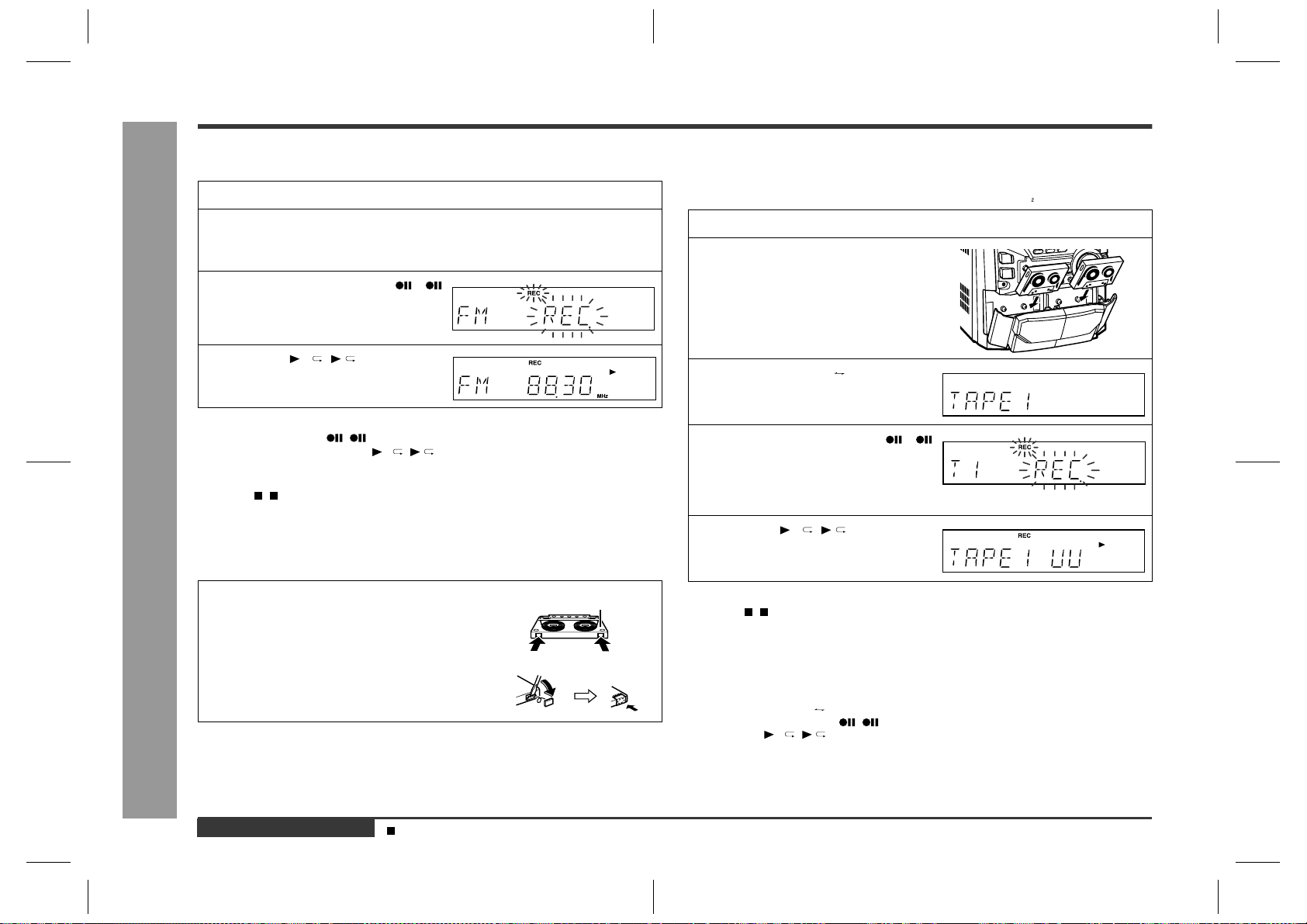
CD-BK110V/CD-BP99V
– 30 –
A
B
C
D
E
F
G
H
1
23456
• NOTES ON SCHEMATIC DIAGRAM can be found on page 16.
Figure 30 SCHEMATIC DIAGRAM (11/14)
64
63
62
61
60
59
58
57
56
55
54
53
52
51
50
49
48
47
46
45
44
43
42
41
40
39
38
37
36
35
34
33
32
31
30
29
28
27
26
25
24
23
22
21
20
19
18
17
16
15
14
13
12
11
10
9
8
7
6
5
4 3 2
2
1
1
AUEMP
AV_GND
D_GND
RES
TEST POINT
MBUSY
+5V
+B
+B
+B
+B
+B
+B
+B
+B
+B
+
+B
+B
+B
+B
DATAD
C2PO
BCLK
LRCK
SBUSY
AULRCK
AUDO
AUCLK
AUBCK
MCLK
MDO
MDI
3.3V
TO CD SECTION
P33 11 - C/P33 11 - F
GND
SCK
SI
SO
RESET
VDD
VPP
TO CD SECTION
P33 11 - C/P33 11 - E/P33 11 - F
7
6
5
4
1
2
3
KEY CONT.
VOCAL CANCEL
HD0
HD1
K_C_STRB
K_C_CLK
K_C_DATA
VSS0
VDD0
PWR_MPEG
MDI
MDO
MCK
SBUSY
MBUSY
VDD1
AVSS
HD7
HD6
HD5
HD4
HD3
HD2
AVREF
AVDD
RESET
XT2
XT1
IC
X2
X1
VSS1
INT
HCS
HRD
HWR
HDAK
HA
MPEG RESET
CD-LD M-
CD-LD M+
CD-SOL
MO_SPEED
2
3
1
10
8
18
4
3
2
16
11
12
14
13
15
19
17
6
1
7
5
9
6.5V
6.2V
5V
0V
10V
10.2V
10.2V
8.8V
ICV1
IX0352AW
MPEG CONTROLLER
QV2
KTA1298 Y
CV1
47/10
RV1
10K
RV2
1K
DV4
1SS133
QV3
KRC102 M
RV86
4.7K
RV11
1K
CV4
47/6.3
CV5
0.22
L64
0.82µH
RV93 10K
RV15
1K
RV94 10K
CV2
0.22
RV20
1K
XV1
4.19 MHz
RV22
1K
RV59 10K
RV37
1K
RV38 3.9K
RV39 3.9K
RV40 3.9K
RV41 3.9K
RV42 3.9K
RV43 3.9K
RV44 3.9K
RV45 3.9K
RV46 3.9K
RV47 3.9K
RV48 3.9K
RV49 3.9K
RV50 3.9K
CV10
47/10
CV9
0.022
CV7
27P
XV2
XV2
27M Hz
CV6
27P
CV11
0.022
RV85
10K
RV84
4.7K
DV5
1SS133
QV4
KTA1298 Y
0V
RV92
0
RV51
47K
CV44
27P
CV45
27P
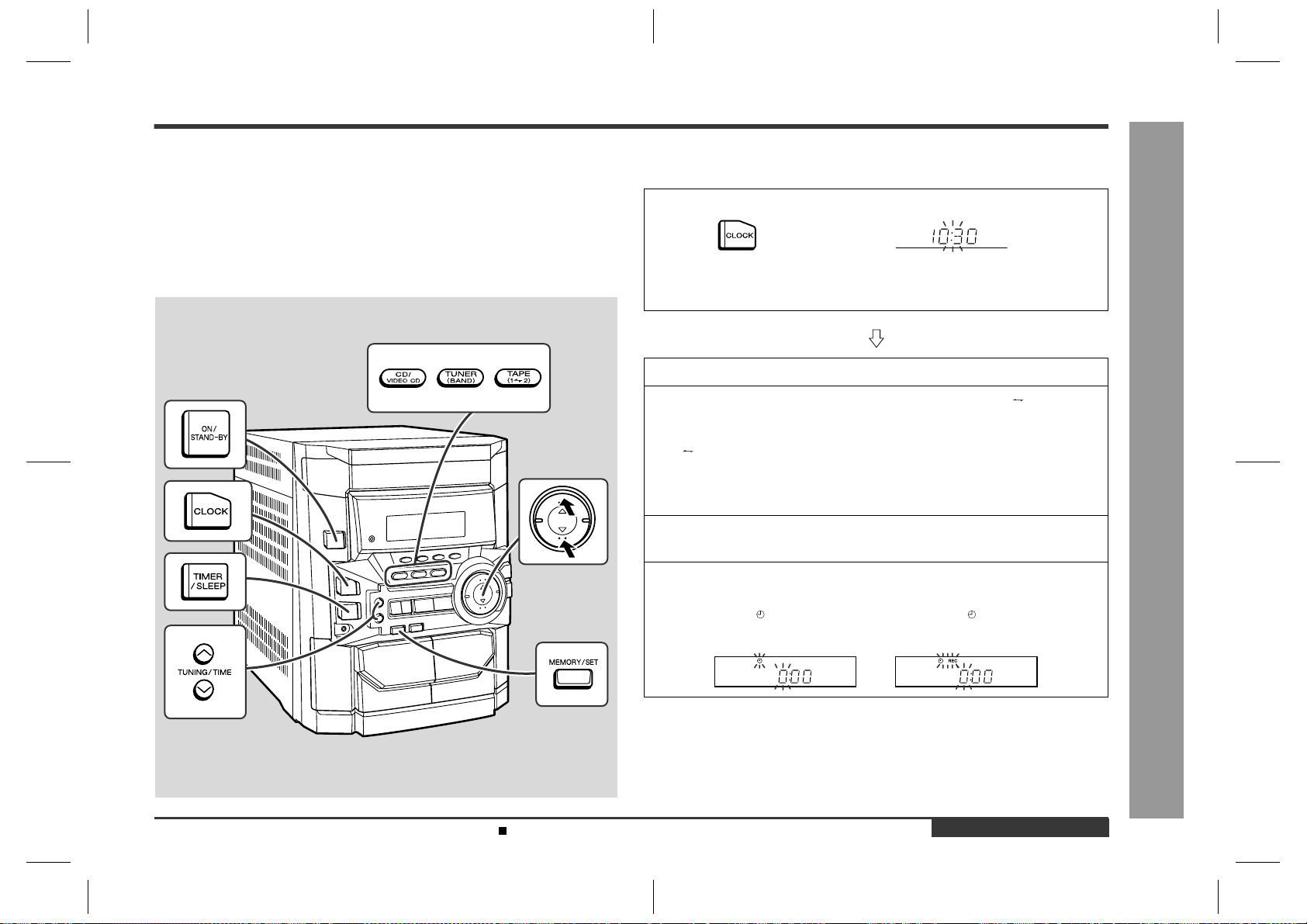
– 31 –
CD-BK110V/CD-BP99V
Figure 31 SCHEMATIC DIAGRAM (12/14)
7
8 9 10 11 12
8
7
6
5
4
3
2
1
100
100
99
99
98
97
96
95
94
93
92
91
90
89
88
87
86
85
84
83
82
81
80
79
78
77
77
76
76
75
74
73
72
71
70
69
68
67
66
65
64
63
62
61
60
59
58
57
56
55
54
53
52
51
50
50
49
49
48
47
46
45
44
43
42
41
40
39
38
37
36
35
34
33
32
31
30
29
28
27
27
26
26
25
24
23
22
21
20
19
18
17
16
15
14
13
12
11
10
9
8
7
6
5
4
3
2
1
40
39
38
37
36
35
34
33
32
31
30
29
28
27
26
25
24
23
22
21
20
19
18
17
16
15
14
13
12
11
10
9
8
7
6
5
4
3
2
1
+B
+B
+B
+B
+B
+B
+B
+B
+B
+B
2
1
CDBCK
CDLRCK
CDEMPH
CDC2PO
AGND
VOUT3
VOUT2
VOUT1
CBP3
CBP2
CBP1
AVDD
HSYNC
NSYNC
CSYNC
VCLK
VCLK
CDI
MD8
MD9
MD10
MD11
GND
MD12
MD13
MD14
MD15
MD0
MD1
MD2
MD3
MD4
MD5
MD6
MD7
MCAS
MWE
VDD
VDD
VDD
VDD
VDD
MRAS
MA0
MA1
MA2
MA3
VDD
MA4
MA5
MA6
MA7
MA8
VDD
AUDO
AUEMPH
AULRCK
AUBCK
AUCLK
INT
HDAK
RESET
VDD
HSELA
HSELX
HA
HWR
HRD
HCS
VDD
CKSEL
VDD
X2
X1
HD0
HD1
HD2
HD3
GND
GND
GND
GND
GND
GND
GND
GND
GND
GND
GND
GND
GND
GND
HD4
HD5
HD6
HD7
GND
VDD
VSS
DQ15
DQ14
DQ13
DQ12
VSS
DQ11
DQ10
DQ9
DQ8
LCAS
UCAS
OE
A8
A7
A6
A5
A4
VSS
VDD
A3
A2
A1
A0
RAS
WE
DQ7
DQ6
DQ5
DQ4
VDD
DQ3
DQ2
DQ1
DQ0
VDD
VIDEO SIGNAL
VIDEO CD PWB-E(1/2)
1
2
1
2
D919
1SS133
D920
1SS133
BI902
CNS902
JK902
VIDEO OUT
JACK
VIDEO OUT
PWB-J
CV10
47/10
CV9
0.022
CV7
27P
XV2
XV2
27M Hz
CV6
27P
CV11
0.022
RV64
47
RV95
6.8K
ICV4
NJM2267M
VIDEO
OPERATION AMP.
CV39
1000/6.3
CV40
22/10
CV41
4.7/50
RV96
33K
CV17 0.01
CV18 1000/6.3
RV61
100K
CV15
4.7/50
RV60
100
CV13
0.1
CV14
0.1
CV16
0.1
ICV2
D61012GC
MPEG DECODER
CV12
0.022
CV20
0.022
L63
0.82µH
CV23
47/10
CV25
0.22
ICV3
SDM4260C
DRAM
CV24
0.22
CNPV3
RV63
150
RV62
150
CV22
47/10
CV19
0.022
CV21
0.022
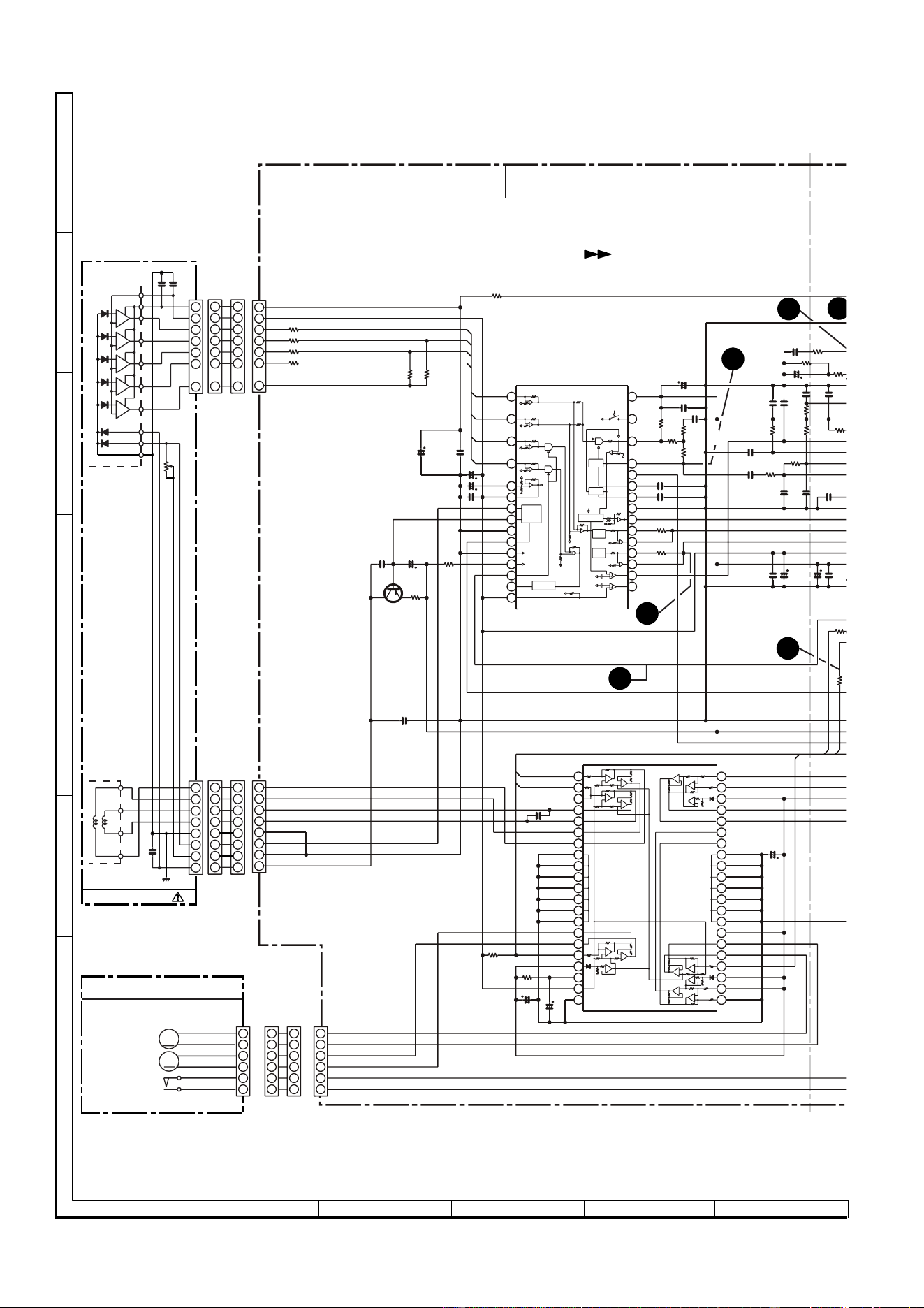
CD-BK110V/CD-BP99V
– 32 –
A
B
C
D
E
F
G
H
1
23456
• NOTES ON SCHEMATIC DIAGRAM can be found on page 16.
Figure 32 SCHEMATIC DIAGRAM (13/14)
CD MOTOR PWB-H
PICKUP UNIT
TR-
TR+
FO+
FO-
GND
ACTUATOR
FO+
FO-
TR-
TR+
PD
VR
LD
5
2
8
3
6
7
1
4
1
2
3
4
5
6
7
88
3
6
7
1
4
5
2
Vcc
C
Vref
F
B
E
A
2
5
3
1
7
6
4
5
1
3
7
6
4
2
4
3
2
1
7
6
5
CNS1A
CNS1B
CD SIGNAL
+B
+B
+B
+B
+B
+B
LD
VR
PD
GND
FO–
FO+
TR+
TR–
1
2
3
4
5
7
6
9
10
11
12
13
14
15
16
17
18
19
20
21
22
23
24
25
26
27
28
29
30
8
7
6
5
4
3
2
1
N.C.
N.C.
LDON
EFBL
FIN1
FIN2
REF1
TIN2
TIN1
N.C.
AGON
LDD
TEST0
TEST
HFL
TE
TE–
FE
FE–
RFEV
BH
PH
RF
RF–
RFSW
VCC
GND
VREF
TES1
NC
REF
ODRV
AGCON
ODRV
REF
REF
REF
REF
REF
REF
REF
REF
REF
REF
REF
REF
REF
REF
AGCON
ODRV
APC
LPF
DH
PH
LPF
LPF
PH/BH
PC
K
FDO
TDO
T
BH
PH
ADA
V
ADA
V
V
PH(RF
E
JI
JI
E
F
S
L
S
L
V
V
V
V
P
D
PD01
N.C.
9
10
11
12
13
14
15
16
17
18
19
20
21
22
23
24
25
26
27
28
29
30
31
32
33
34
35
36
37
38
39
40
41
42
8
7
6
5
4
3
2
1
N.C.
N.C.
SLDO
FDO
TDO
LOADING M–
VCC3
VCC2(SPN)
VCC4
LD_M+
LD_M–
LOADING M+
SP–
SP+
SPO
MUTE
Vref
STANDBY
VCC1
SL–
SL+
GND
GND
TR+
TR–
FO–
FO+
FO
FD
TO
+
+
+
+
+
–
–
–
–
–
+
–
+
–
+
–
–
–
–
+
+
+
+
–
+
–
+
–
+
–
8
7
6
5
4
3
2
1
GND(D)
PUIN
SP+
SP–
SL+
SL–
6
2
3
1
4
5
6
2
3
1
4
5
6
2
3
1
4
5
6
2
3
1
4
5
M
M
+
-
-
+
TDO
FDO
SPDO
EFBL
FIN2
FIN1
TIN2
TIN1
VIDEO CD PWB-E(2/2)
7
8
1.5V
C8
0.022
C7
10/16
C20
0.1
C14
0.33
R56
56K
R55
56K
R54 68K
R53 56K
R52 56K
R51 68K
CNP1
CNP2
C54
47/10
C13
0.01
R50
47
C47
100/10
C55
0.01
C51
47/10
C53
0.001
R47
3.3
Q3
KTA1504 GR
CNP3
C41
100/10
R8
330
C11
47/10
R10
27K
C26
0.047
C22
100P
R80
1M
C49
100/10
C50
100/10
R79
1.5M
C24
2.2/50
C21
0.1
C23
0.047
R12
680
R35
1K
C52
0.01
R25
10K
R14
1.2K
R11
12K
R13
680
C81
0.0
2
R6
27K
C27
0.1
C28
47/10
C82
0.022
R7
6.8K
R44
1K
C17
0.0047
S
E
R5
39K
C12
0.022
C46
0.022
R15
10K
C18
6P
R3
47K
C2
9
0.0
2
R4
10K
C42
68P
C25
0.022
IC3
FOCUS/TRACKING/
SPIN/SLED DRIVER
R48
6.8K
CNS3A
CNS3B
M1
SPINDLE
MOTOR
M2
SLED
MOTOR
SW4
PICKUP IN
CNP3A
CNS2A
CNS2B
IC1
LA9235M
SERVO AMP.
R42
56K
IC3
M63001FP
C6
100/10
5
4
13
1
2.3V
2.7V
LASER
DRIVER
R2
1.5K
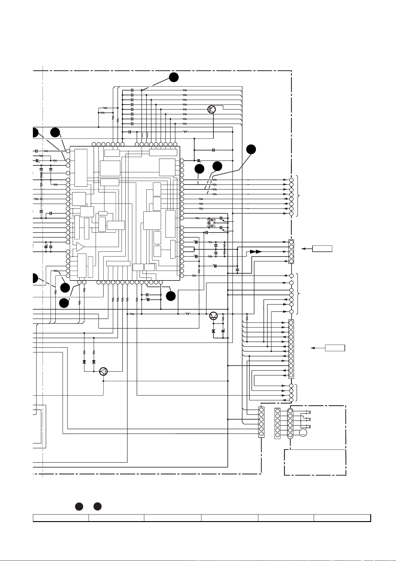
– 33 –
CD-BK110V/CD-BP99V
Figure 33 SCHEMATIC DIAGRAM (14/14)
7
8 9 10 11 12
• The numbers 1 to 13 are waveform numbers shown in page 44.
5
2
1
4
3
6
5
2
1
4
3
6
5
2
1
19
18
17
16
4
3
6
DISC_NO
GND(D)
M–
M+
M
RES
C2PO
SBUSY
MBUSY
TO
MPEG
SECTION
P30 1 - C,
P30 1 - F
MBUSY
SBUSY
DRF
GND
CD RES
CLK
WRQ
CDINT
CLAMP SW
DI
DO
CE
DO
INT
DRF
WRQ
CE
RES
DI
CL
AUEMP
3.3V
MCLK
MDI
MDO
D_GND
AV_GND
+5V
DGND
AGND
L-CH
R-CH
5
4
3
2
1
+5V
+B
+B
+B
+B
+B
+B
AULRCK
AUBCK
AUDO
LRCK
BCLK
DATAD
AUCLK
TO
MPEG
SECTION
P30 1 - C,
P30 1 - F
14
15
13
12
11
10
9
8
7
6
5
4
3
2
1
O/C
TO
MPEG
SECTION
P30 1-C,
P30 1-F
CNS601
P20 1 - B
FROM MAIN PWB
P29 12 - B
CNS702
FROM
DISPLAY PWB
9
10
11
12
13
14
15
16
17
18
19
20
21
22
23
24
25
26
27
28
29
30
31
32
33
34
35
36
37
38
39
40
41
42
43
44
45
46
47
48
49
50
51
52
53
54
55
56
57
58
59
60
61
62
63
64
65
66
67
68
69
70
71
72
73
74
75
76
77
78
79
80
8
7
6
5
4
3
2
1
N.C.
N.C.
N.C.
NC
N.C.
N.C.
N.C.
N.C.
N.C.
N.C.
FG(D_Vref)
C2F
PCKIST
TEST
DOUT
VDD
PCK
SLDO
SPDO
FDO
TDO
TBLO
BHREF
PHREF
ADAVSS
ADAVDD
VREF
TE
FE
PH(RFENV)
BH
JITTC
JITTV
EFMIN
SLCO
SLCIST
HFL
FR
VVDD
VVSS
PD02
PD01
EMPH
MUTEL
MUTER
LVDD
LCHO
XVDD
LVSS
RVSS
RCHO
RVDD
XIN
XOUT
XVSS
ASLRCK
ASDACK
ASDFIN
LRSY
DATACK
DATA
16M
SFSY
SBSY
PW
SBCK
VDD5V
EFMO
N.C.
EFLG
FSX
CONT5
CONT4
CONT3
CONT2
CONT1
LASER
SERIAL
OUT
EXTERNAL
AUDIO IN
DIGITAL
FILTER
1BIT
DAC
LPF
INTERPOLATION
MUTE
ATTENUATION
DEEMPHASIS
AUDIO
OUT
ERROR
CORRECT
FRAME SYNC
DEFECT,PROTECT
EFM DECODE
CLV
CONTROL
CLOCK
GENERATOR
GENERAL
SUBCODE
DECODE
CRC
COMMAND
INTERFACE
GENERAL
SW
SERVO
PROCESSEROR
AUTO
ADJUST
–
+
S/H
JITER
DEFECT
CONTROL
A/D
SW
SLICE
LEVEL
CONTROL
PLL
VCEC
D/A
CONT7
CONT6
CE
CL
DI
DO
WRQ
RES
DEF
VSS
V/vP
FSEQ
DEFECT
32
1
TDO
SLDO
FDO
RES
WRQ
CE
CL
DI
DRF
INT
O/C
DISC_NO
9
10
11
12
8
7
1
5
6
4
2
3
+
–
CD LOADING
MOTOR PWB-G
EFBL
9
10
11
12
3
7
8
R97
3.9K
R96
1K
R19
47
C64
47/10
ZD61
DZ3.9BSB
C56
470/6.3
R20
220
R16
10K
L61
0.82µH
Q4
KTA1504 GR
C34
0.022
XL1
16.93 MHz
C45
100/10
R1
1K
R89 1K
R91 1K
R90 1K
R93 1K
R92 1K
R86 1K
R85 100
R95
4.7K
R94
3.3K
R67
1K
R68
1K
C83
0.022
R84
10K
C40
0.0015
C43
0.0015
R83
10K
R82
3.9K
R81
3.9K
R17 1K
D21
1SS133
R21
470
R22
470
Q2
KRC102 M
D22
1SS133
R46 1K
R45 1.2K
R40 1.2K
C80
0.1
R73 1K
R71 1K
C72 100P R72 1K
C71 100P
C73 100P
C75 100P
C76 100P
C77 100P
C78 100P
R75 1K
R76 1K
R77 1K
R78 1K
C74 100P R74 1K
L62
2.2µH
C38
10/16
C39
10/16
CNP4
4
1
/
10
C26
0
.047
C22
100P
R80
1M
R
79
.5M
C24
2.2/50
C21
0.1
C23
0
.047
R12
680
R35
1K
R39
470
R38
270
C44
0.022
C31
100/10
R14
1.2K
R11
12K
R13
680
C81
0.022
C27
0.1
C28
47/10
R44
1K
IC2
SERVO/SIGNAL
CONTROL
R58
220
Q1
KTC3265 Y
C30
0.022
R15
10K
C29
0.022
DO
SW3
DISC NUMBER
SW2 CLAMP
SW1
OPEN/CLOSE
M3
T/T UP/DOWN
LOADING MOTOR
BI4
CNS4
IC2
LC78636E
2
1
6
CNP12
CNP11
10V
10V
0V
3.3V
4V
5V
1V
0V
0V
CONSTANT
VOLTAGE
C58
27P
C57
27P
CD-BK110V/CD-BP99V
– 34 –
A
B
C
D
E
F
G
H
1
23456
Figure 34 WIRING SIDE OF P.W.BOARD (1/9)
C141
L104
R137
1234567
123
R138
C105
C150
C119
CNP101
CN102
FROM
TAPE 2 RECORD/
PLAYBACK HEAD
FROM TAPE 1
PLAYBACK HEAD
C104
C103
C115
C113
C139
C135
C133
C131
C127
CNP901
654321
C129
C137
C138
C145
C959
C953
C958
C952
C947
D914
D912
D911
D913
C951 C950
C912
C914
R910
R912
R913
R911
R908
C91
0
R926
C944
C945
SW801
VOLTA
G
SELECT
O
C908
C904
C903
D917
D103
R128
R150
Q103
R143
R140
R141
C128
C136
D916
C946
C911
C917
R914
R915
R928
C954
R930
ZD903
R929
Q904
R927
C956
ZD902
C957
C955
Q902
Q901
C913
C916
F901
T2.5A L 250V
D910
D908
D909
D907
D915
C130
C132
C126
C134
C123
IC101
C112
C114
C120
C146
C118
R120
R124
C116
R117
R115
R119
R135
R127
F902
T1.6A L 250V
R121
R133
R139
R136
R132
R123
R122
R125
R607
R142
R130
R129
R151
D101
D102
C122
C110
C603
R617
R625
D902
CNP701
1
3
5
7
9
11
13
15
17
19
21
2
4
6
8
10
12
14
16
18
20
R411
R419
R414
R425
R423
JP402
CNP801
2
110V
127V
C413
R427
R410
R417
R421
C414
R422
Q403
C409
R429
R412
R433
R439
Q404
R426
R428
R424
3
2
1
R405
Q405
Q407
R415
R437
R418
R420
R363
R364
R362
C369
C366
C365
C363
C364
C367
T303
C361
C362
C330
C335
T306
R323
VD301
VD303
R322
R325
R327
VD302
C334
C314
C310
C315
D305
R314
R313
L312
C323
C321
D302
CNP302
SW601
SPAN
SELECTOR
SO901
SPEAKER
TERMINAL
+
-
D301
50/9 kHz
75 OHMS GND
100/10 kHz
C368
C374C371
R357
R356
C331
C332
R351
R365
R311
R358
R350
TP302
C372
L-CH
+
-
R-CH
R361
R355
C399
C398
C373
IC303
R353
C433
Q407
C357
C358
R436
R416
Q408
Q406
R435
Q602
C602
R604
C440
R438
R432
C441
R610
R430
R360
C608
C612C610
R616
R372
R378
R359
R386
D306
R395
L351
R388
R387
R377
C396
C395
C320
C356
C355
R352
R393
C386
C387
R383
R382
R379
T351
R380
R336
T302
C312
Q360
R316
C313
C324
C311
C317
C318
C316
R375
R302
T301
B
C
E
R309
Q302
D304
C393
C342
C307
C308
C305
C303
BF301
C304
SO302
FM ANTENNA
TERMINAL
C301
C304A
D304A
D303A
C309
D303
IC301
C306
CF302
R381
C322
C302
CF352
R385
C394
C391
C380
C397
C392
C385
C351
C352
C350
C381
IC302
R384
C319
X352
C382
C412
L352
R376
CF351
C353
C354
X351
C370
R434
C411
R608
BI601
5
1
C147
C601
Q601
R601
R603
R134
R131
C121
R105
C102
C117
Q106
Q104
Q107
Q105
Q110
Q111
Q102
R107
R103
R109
R110
R112
R102
R101
R144R145
C109
C605
C604
R615
C611
C609
C607
R609
C623
C420
C617
C616
R374
C613
C629
C625
C627
C628
C421
C626
C630
IC601
C606
C614
C618
C615
R373
C619
C624
R618
R602
R431
R157
R106
R148
R146
L103
R147
R114
C107
R104
R126
R116
R113
R111
R118
C140
C148
C142
C106
C108
C101
Q114
Q109
Q108
Q101
Q113
Q112
R149
R108
1
510
1520
1
2
3
1
2
3
4
5
6
7
8
9
24
13
24
20 15
13
12
1
5
10
12
24
20 15
13
1
5
10
12
22
20 15
12
1
5
10
11
1
5
12345
CNS601
GY
WH
GY
WH
RD
CNP11
P40 3 - A
TO VIDEO CD PWB
FROM
TAPE MECHANISM GND
B C E
B C E
E C B
E C B
E
C
B
E
C
B
E
C
B
B C E
B C E
B C E
1 2 3
1 2 3
E
C
B
1
2
3
E C B
B
C
E
1 2 3
B C E
TP301
3
2
1
12
12
AM LOOP
ANTENNA
E
B
C
C B E
C B E
C B E
E
B
C
E B C
E
C
B
1 2 3
1 2 3
1
2
3
4
5
P42 5 - E
P42 5 - E
LUG1
CD-BK110V

– 35 –
CD-BK110V/CD-BP99V
Figure 35 WIRING SIDE OF P.W.BOARD (2/9)
7
8 9 10 11 12
AC POWER SUPPLY CORD
AC 110/127/220/230-240 V
50/60 Hz
C912
C914
R910
R912
R913
R911
R908
R907
R905
C907
C934
C935
C910
R926
C943
D918
C944
C945
R917
R916
JK901
HEADPHONES
R408
Q401
C403
C404
Q402
C402
R404
R403
1
R402
R401
R407
R409
JK1
MIC
C406
C405
C401
C408
SO902
SW801
VOLTAGE
SELECTOR
3
IC904
3
2
1
C908
C904
C903
Q905
B
C
E
R923
D922
C938
IC902
C940
3
2
1
C939
R925
C909
R922
R906
C915
R909
C905
IC901
C918
C933
C946
C911
C906
C919
C917
R914
R915
5
5
Q902
Q901
C913
C916
D907
1
21
3
2
1
SOK2
TO DISPLAY PWB
CNP801
220V
WH
RD
BK
WH
RD
BK
230-240V
110V
127V
+
1
2
3
4
5
6
7
8
9
10
11
12
54321
12345
PW901B
HEADPHONES
PWB-D
MIC PWB-C
MAIN PWB-A
5
6
4
3
2
1
YL
YL
BR
BR
WH
WH
CNS901
PT801
POWER
TRANSFORMER
RD
OR
BR
YL
BL
CNS801
3
2
1
4
5
1 2 3
1 2 3
PW901A
VR401
MIC
VOLUME
E B C
C
B
E
AC INPUT SOCKET
AC 110/127/220/230-240 V
50/60 Hz
BR
COLOR TABLE
RD(R)
OR
YL
GR
BL
VL
GY
WH(W)
BK
PK
BROWN
RED
ORANGE
YELLOW
GREEN
BLUE
VIOLET
GRAY
WHITE
BLACK
PINK
1
2
3
4
5
JP401
P39 10 - H
FFC701
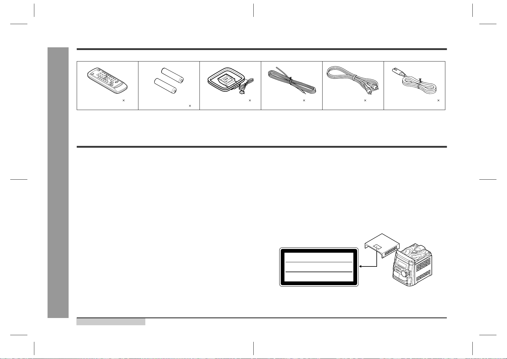
CD-BK110V/CD-BP99V
– 36 –
Figure 36 WIRING SIDE OF P.W.BOARD (3/9)
A
B
C
D
E
F
G
H
1
23456
12345
CNS601
GY
WH
GY
WH
RD
C141
L104
R137
123
R138
C105
C150
C119
CNP101
CN102
C104
C103
C115
C113
C139
C135
C133
C131
C127
CNP901
C129
C137
C138
C145
C959
C953
C958
C952
C947
C916
D914
D912
D911
D913
C951
C950
C908
R901
R
9
C
C904
D917
D103
R128
R150
Q103
R143
R140
R141
C128
C136
D916
C946
R928
R910
C954
R930
ZD903
R929
Q904
R927
C956
ZD902
C957
D901
C955
F901
T2.5A L 250V
D910
D908
D909 D907
D915
C130
C132
C126
C134
C123
IC101
C112
C114
C120
C146
C118
R120
R124
C116
R117
R115
R119
R135
R127
R121
R133
R139
R136
R132
R123
R122
R125
R607
R142
R130
R129
R151
D101
D102
C122
C110
C603
R617
R625
D902
CNP801
R363
R364
R362
C369
C366
C365
C363
C364
C367
T303
C361
C362
C330
C335
T306
C331
VD301
VD303
R322
R325
R327
VD302
C334
C314
C310
C315
D305
R314
R313
L312
C323
C321
D302
CNP302
D301
C368
C374
C371
R357
R356
R323
C332
R351
R365
R311
R358
R350
C372
R361
R355
C399
C398
C373
IC303
R353
C357
C358
Q602
C602
R604
R610
R360
C608
C612
C610
R616
R372
R378
R359
R386
D306
R395
L351
R388
R387
R377
C396
C395
C320
C356
C355
R352
R393
C386
C387
R383
R379
T351
R380
R336
T302
C312
Q360
R316
C313
C324
C311
C317
C318
C316
R375
R302
T301
R309
Q302
C393
C342
C307
C308
C305
C303
BF301
C304
D304
C301
C304A
D304A
D303A
C309
D303
IC301
C306
CF302
R381
C322
C302
CF352
R385
C394
C391
C397
R382
C380
C392
C385
C351
C352
C350
C381
IC302
R384
C319
X352
C382
L352
R376
CF351
C353
C354
X351
C370
R608
BI601
5
1
C147
C601
Q601
R601
R603
R134
R131
C121
R105
C102
C117
Q106
Q104
Q107
Q105
Q110
Q111
Q102
R107
R103
R109
R110
R112
R102
R101
R144
R145
C109
C605
C604
R615
C611
C609
C607
R609
C623
C617
C616
R374
C613
C629
C625
C627
C628
C626
C630
IC601
C606
C614
C618
C615
R373
C619
C624
R618
R602
R157
R106
R148
R146
L103
R147
R114
C107
R104
R126
R116
R113
R111
R118
C140
C148
C142
C106
C108
C101
Q114
Q109
Q108
Q101
Q113
Q112
R149
R108
F902
T1.6A L 250V
1
5
1234567
654321
CNP701
1
3
5
7
9
11
13
15
17
19
21
2
4
6
8
10
12
14
16
18
20
SO901
SPEAKER
TERMINAL
+
-
L-CH
+
-
R-CH
SW601
SPAN
SELECTOR
50/9 kHz 100/10 kHz
75 OHMS GND
SO302
FM ANTENNA
TERMINAL
1
2
3
1
5
10
1520
24
13
12
24
20
15
13
1
5
10
12
22
20 15
12
1
5
10
11
1
2
3
4
5
6
7
8
9
24
20
15
13
1
5
10
12
FROM
TAPE 2 RECORD/
PLAYBACK HEAD
FROM TAPE 1
PLAYBACK HEAD
FROM
TAPE MECHANISM GND
CNP11
P40 3 - A
TO VIDEO CD PWB
B C E
B C E
E C B
E C B
E C B
E
C
B
E
C
B
E
C
B
E
C
B
1
2
3
B C E
B C E
B C E
1 2 3
1 2 3
B
C
E
B C E
TP301
B
C
E
TP302
3
2
1
1 2 3
12
12
AM LOOP
ANTENNA
E
C
B
1
2
P42 5 - E
P42 5 - E
LUG1
R931
CD-BP99V
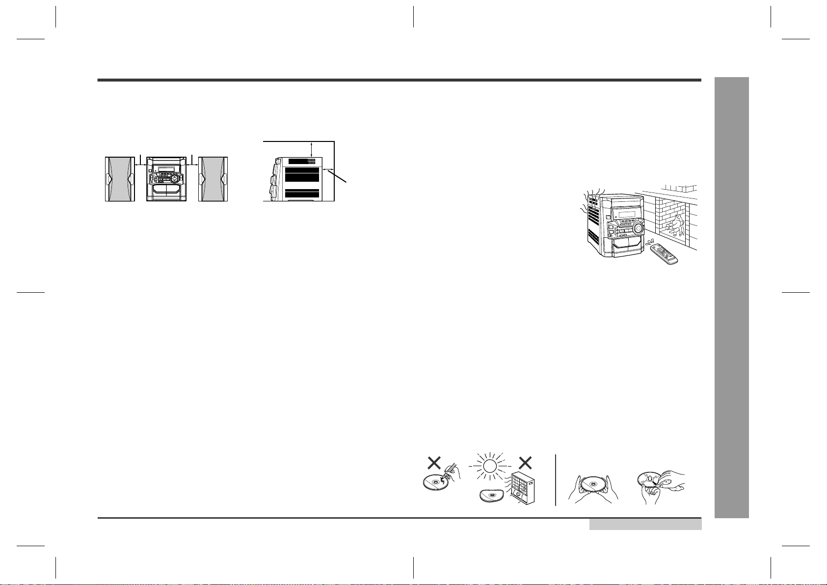
– 37 –
CD-BK110V/CD-BP99V
Figure 37 WIRING SIDE OF P.W.BOARD (4/9)
7
8 9 10 11 12
54321
12345
C916
C908
C933
C905
C906
C907
C934
C935
R901
R902
R926
C943
D918
C944
C945
R917
R916
SO902
IC904
C901
C904
C903
Q905
B
C
E
R923
D922
C938
IC902
C940
C939
R925
C902
R922
C912
R903
R904
C911
C914
IC901
C946
R910
C954
D901
C955
D
909 D907
CNP801
PW901B
JK901
HEADPHONES
+
C
H
3
2
1
3
2
1
1
2
3
4
5
6
7
8
9
10
11
12
1
21
SOK2
TO DISPLAY PWB
5
6
4
3
2
1
YL
YL
BR
BR
WH
WH
CNS901
RD
BL
CNS801
1
2
PT801
POWER
TRANSFORMER
PW901A
HEADPHONES
PWB-D
MAIN PWB-A
AC POWER SUPPLY CORD
AC 220-240 V
50/60 Hz
AC INPUT SOCKET
AC 220-240 V
50/60 Hz
1
2
BR
COLOR TABLE
RD(R)
OR
YL
GR
BL
VL
GY
WH(W)
BK
PK
BROWN
RED
ORANGE
YELLOW
GREEN
BLUE
VIOLET
GRAY
WHITE
BLACK
PINK
P39 10 - H
FFC701
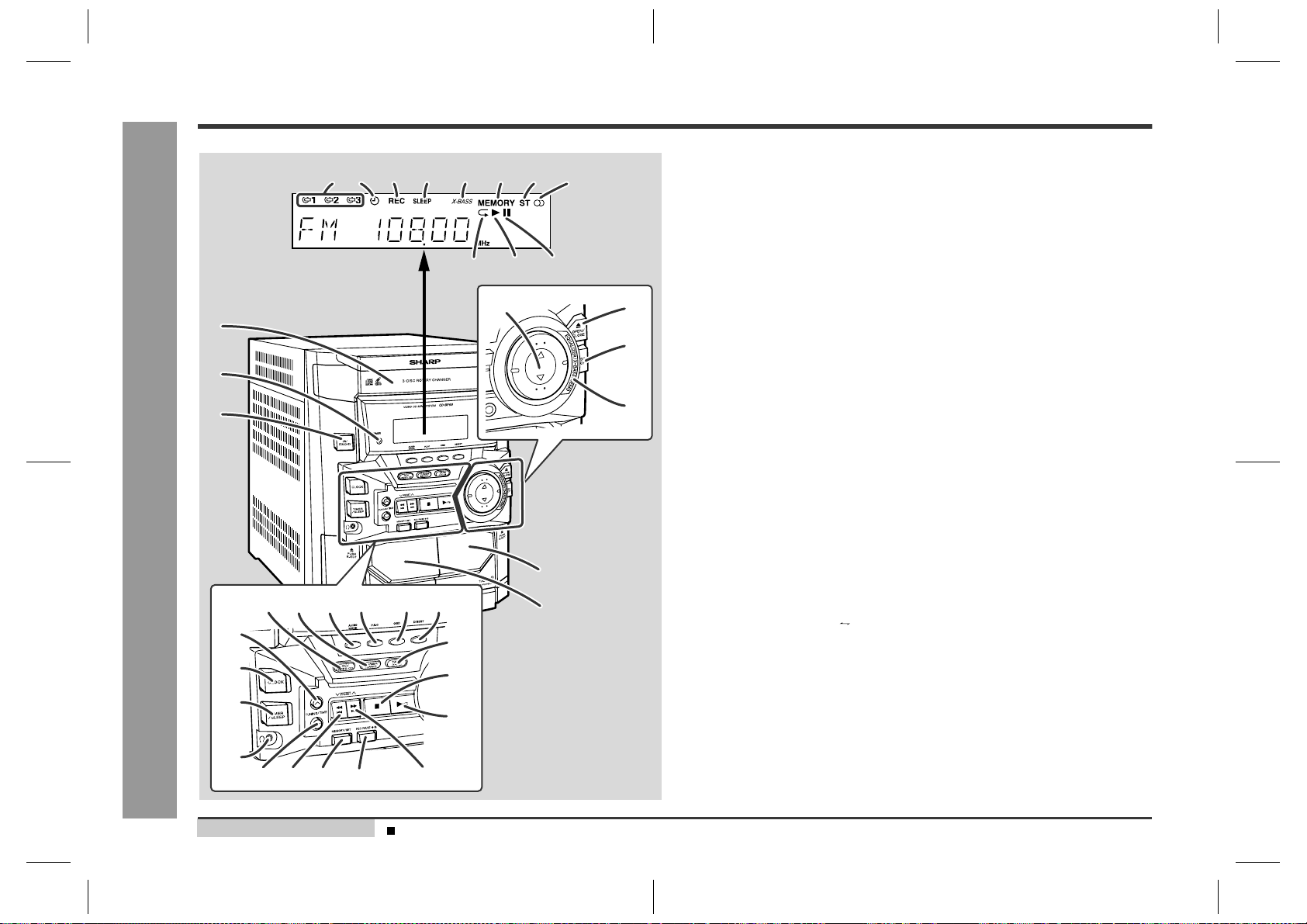
CD-BK110V/CD-BP99V
– 38 –
Figure 38 WIRING SIDE OF P.W.BOARD (5/9)
A
B
C
D
E
F
G
H
1
23456
R771
D709
Q707
C714
C716
C701
Q701
R779
R706
R707
XL701
R700
R704
R703
R702
R708
RD06
RD07
R714
R715
R716
C703
C704
F3
F4
9G
4G
3G
2G
1G
P17
P18
P19
P1
8G
P2
P3
P12
7G
6G
P4
P5
C707
R768
RD09
RD26
RD10
RD11
RD12
RD08
R728
R727
R726
C718
C717
C710
IC704
C715
R770
R772
R701
R744
100
81
80
30
R
D
SW715
TAPE
TO TAPE MECHANISM PWB
1
246 810
357911
SW720
PLAY
SW712
VOLUME UP
R709
R710
R711
R712
R713
R717
R724
FL
7
FL DI
S
1
5
10
15
20
25
3
65
70
75
85
90
95
R773
R722
R769
R766
R767
D711
D707
L701
D710
C702
C719
C713
C720
Q708
Q705
D703
D702
Q706
Q704
D716
SOK3
SW710
OPEN/CLOSE
SW711
EQUALIZER/
X-BASS/DEMO
SW713
VOLUME
DOWN
RX701
D708
SW709
DISC SKIP
1 2 3
321
1
11
B C E B C E
B C E
3
2
1
3
2
1
1
2
3
IC701
15161718192021222324252627282930313233
DISPLAY PWB-B
P42 2 - A
FFC702
SW707
DIGEST
SW706
OSD
R705
– 39 –
CD-BK110V/CD-BP99V
Figure 39 WIRING SIDE OF P.W.BOARD (6/9)
7
8 9 10 11 12
121
0
1
R718
RD18
RD17
RD16
RD15
3
7G
6G
P4
P5
5G
P6
P7
P8
P9
P10
P11
P14
P20
P13
P16
P15
F2
F1
WH
GY
RD
WH
WH
WH
WH
WH
GY
GY
GY
GY
D714
R745
R742
R737
R734
R735
R743
R748
R749
R751
R750
R736
R729
RD20
RD21
RD22
RD23
RD24
RD19
RD14
RD25
R775
R778
R725
R732
R759
R733
R758
R777
R776
R755
R792
RD03
RD02
RD01
R753
D701
80
51
31
30
R721
R720
R719
RD04
RD05
RD13
SW714
CD
SW724
TUNING UP
SW703
TIMER/SLEEP
SW725
TUNER
(BAND)
SW719
FAST
FORWARD
SW723
REC PAUSE
SW718
REWIND
SW717
MEMORY/SET
SW715
TAPE
SW716
TUNING DOWN
SOK2
CNP701
P35 10 - E (CD-BK110V)
P37 10 - E (CD-BP99V)
TO MAIN PWB
1
2 4 6 8 10 12 14 16 18 20
3 5 7 9 11 13 15 17 19 21
SW721
STOP
1
1 23 456789
10 11 12
BI702
CNS702
P40 3 - A
TO CD SERVO PWB
CNP12
C708
C705
LED722
SW701
ON/STAD-BY
SW702
CLOCK
12
50
FL701
FL DISPLAY
15
20
25
35
40
45
55
60
65
70
75
8
5
IC701
123456789
101112131415161718
BR
COLOR TABLE
RD(R)
OR
YL
GR
BL
VL
GY
WH(W)
BK
PK
BROWN
RED
ORANGE
YELLOW
GREEN
BLUE
VIOLET
GRAY
WHITE
BLACK
PINK
SW705
P.B.C.
SW704
KARAOKE
MODE
FFC701
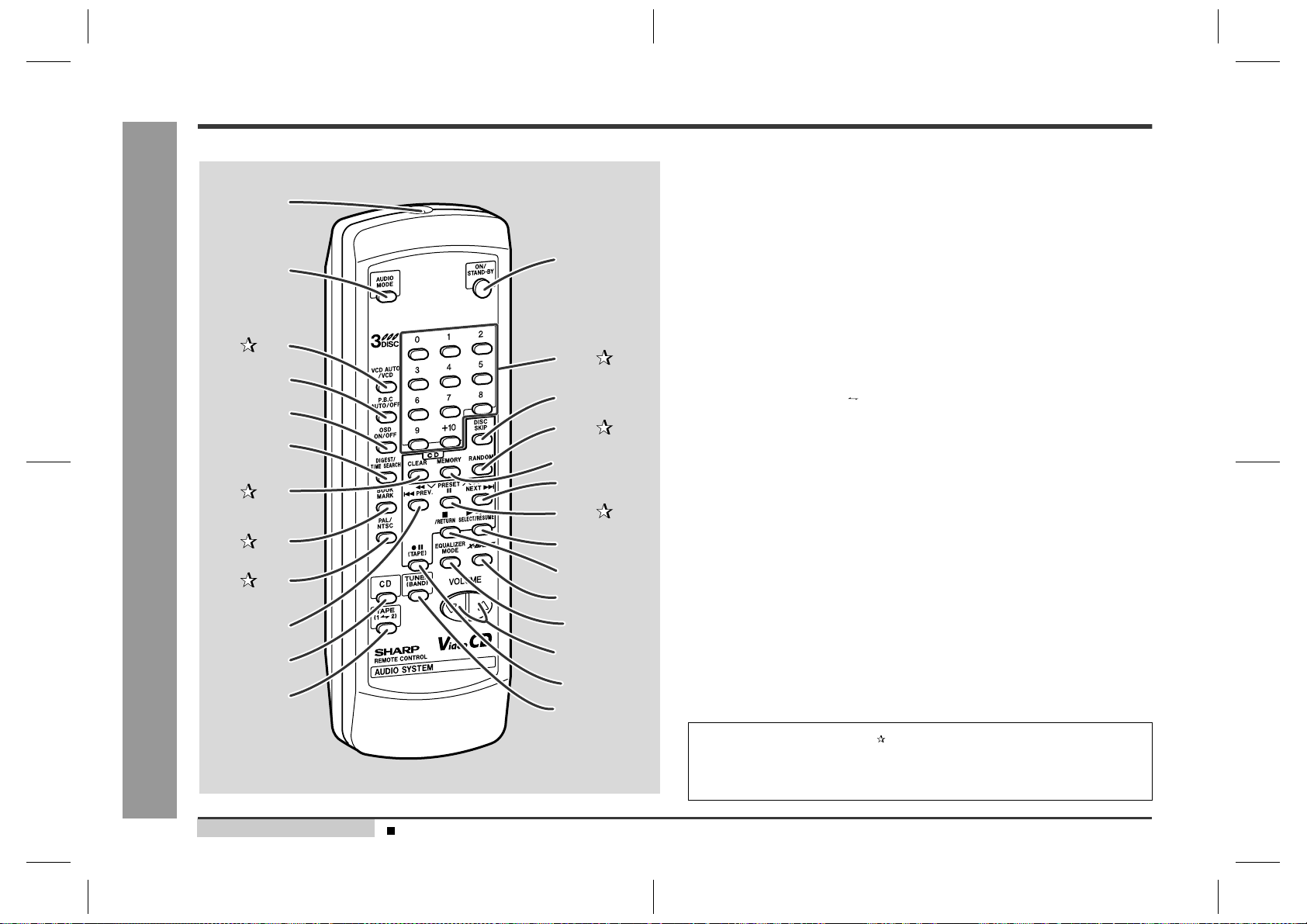
CD-BK110V/CD-BP99V
– 40 –
Figure 40 WIRING SIDE OF P.W.BOARD (7/9)
A
B
C
D
E
F
G
H
1
23456
• The numbers 1 to 13 are waveform numbers shown in page 44.
CNP11CNP12
CV39
CNPV3
CV18
C38
C39
CV15
ICV4
DV4
CV1
DV5
CV41
CV40
1
45
8
C56
XL1
XV1
CV4
L64
XV2
CNP4
CNP3
1
6
1
6
CV10
L63
CV23
1
5
10
15
20
25
26
30 35 40 45
50
51
55
60
65
70
75
76
80859095
100
ICV3
5
10
15
25
30
35
1
20 21
40
C49
C50
D22
D21
C47
CNP1
C6
C54
C7
CV22
C31
C28
C41
C24
C64
ZD61
L61
L62
C45
C11
C51
CNP2
1
7
1
8
ICV2
1
5
1
12
VIDEO CD PWB-E (TOP VIEW)
CNS4
FROM
CD LOADING
MOTOR PWB
P42 1 - F
CNS3A
FROM
PICKUP UNIT
P42 6
-
F
FROM
PICKUP UNIT
P42 6 - G
CNS2A
CNS1A
FROM
CD MOTOR PWB
P42 3 - H
FROM
MAIN PWB
P34 4 - A (CD-BK110V)
P36 4 - A (CD-BK99V)
FROM
DISPLAY PWB
P39 9 - A
CNS902
FROM VIDEO
OUT PWB
P42 2 - C
CNS702
CNS601
12
: Through-hole where the top and bottom patterns are connected.
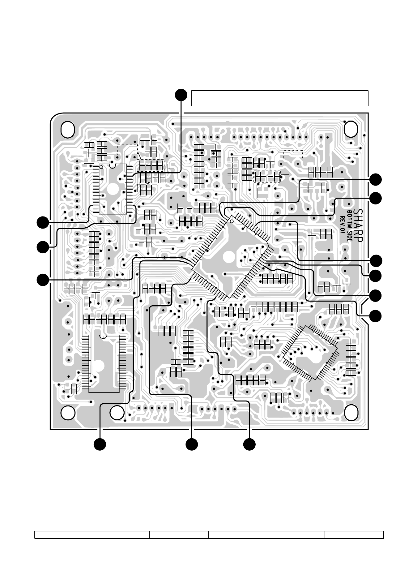
– 41 –
CD-BK110V/CD-BP99V
Figure 41 WIRING SIDE OF P.W.BOARD (8/9)
7
8 9 10 11 12
VIDEO CD PWB-E (BOTTOM VIEW)
R6
C13
R25
C52
C12
R47
C53
Q3
C14
C18
C17
R42
C44
R5
R7
R3
C42
Q1
R4
R8
R58
R68
R95
R94
R67
R97
R82
R84
IC1
5
10
20
25
30
C29
R10
R80
C26
C20
C81
C82
C55
R50
R51
R52
R53
R54
R55
R56
15
16
R1
R16
R17
C30
Q2
C8
R44
R35
C46
R39
R38
R40
R21
R22
R45
CV24
R46
1
42
R2
R48
IC3
5
10
15
20
21 22
25
30
35
40
CV20
CV13
CV14
CV16
CV19
CV25
CV21
R89
R96
R91
R90
R85
CV12
RV11
RV59
RV41
RV51
RV37
RV86
CV5
CV9
CV7
CV6
RV42
RV40
RV39
CV11
R86
R92
R93
C25
C22
C27
R14
R11
C21
R79
C23
R12
R13
RV38
R19
C34
C58
C57
R20
RV43
RV44
RV45
RV46
RV47
RV48
RV49
RV50
IC2
5
10
15
20
24
25
30
35
40 41
45
50
55
R77
C77
R76
C76
C80
C71
C73
R73
C74
R74
C72
R71
R72
C40
R83
C43
R81
C83
64
65
70
75
80
C75
R75
C78
R78
1
RV60
RV62
RV63
RV64
CV17
RV61
RV96
Q4
RV22
CV45
CV44
QV3
QV2
RV84
RV85
QV4
RV2
RV1
ICV1
16
17
1
5
10
15
20
25
30
35
40
45
4849
50
55
60
64
RV20
RV15
RV93
RV94
RV92
CV2
32
33
1
60
RV95
R15
4
13
5
12
11
10
3
961
2
7
8
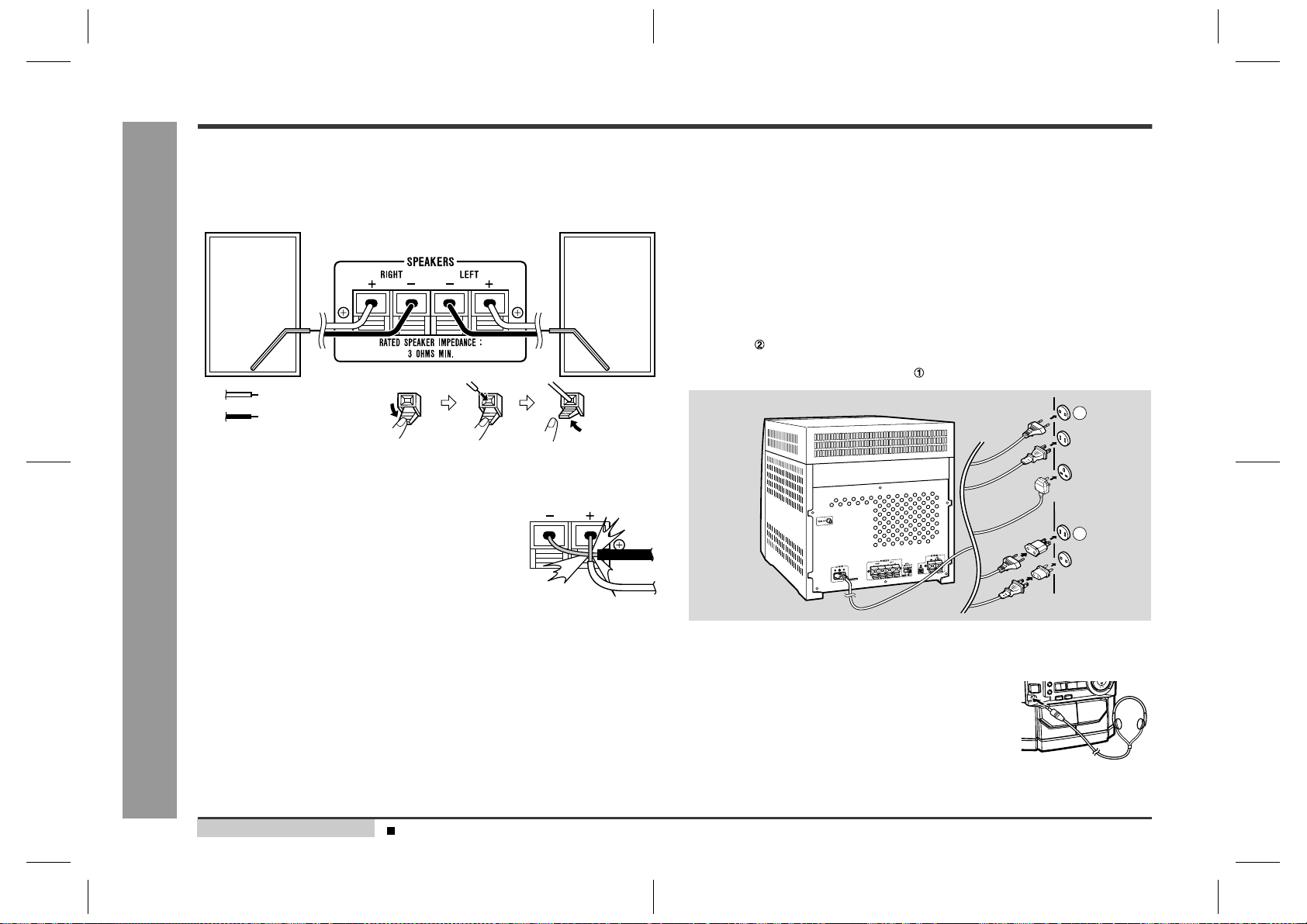
CD-BK110V/CD-BP99V
– 42 –
Figure 42 WIRING SIDE OF P.W.BOARD (9/9)
A
B
C
D
E
F
G
H
1
23456
-
+
SOK3
P38 2 - G
TO DISPLAY PWB
1
2
3
4
5
6
79
11
8
10
SOLENOID
SW
SW
SW
12
SOLENOID
SW
SW
TAPE MECHANISM PWB-F
TAPE MECHANISM
ASSEMBLY
TAPE 2
ERASE HEAD
RECORD/PLAYBACK
HEAD
BL
WH
YL
BK
WH
BK
PK
WH
BK
GR
GR
BL
YL
WH
PK
TAPE
MOTOR
7 6 5 4 3 2 1
CNP102
TAPE 1
PLAYBACK HEAD
BK
WH
PK
BK
WH
GR
23
1
PK
CNP101
BR
COLOR TABLE
RD(R)
OR
YL
GR
BL
PK
BROWN
RED
ORANGE
YELLOW
GREEN
BLUE
PINK
P34 3 - A (CD-BK110V)
P36 3 - A (CD-BP99V)
TO MAIN PWB
P34 2 - A (CD-BK110V)
P36 2 - A (CD-BP99V)
TO MAIN PWB
VL
GY
WH(W)
BK
VIOLET
GRAY
WHITE
BLACK
1
11
FFC702
F3895AF
1
B
TO HEAT SINK
-
+
-
+
–
+
230-0110V-004
AV PCB
230-0099V-004
AV PCB
WH
BK
WH
BK
CNP2
TO VIDEO CD
PWB
P40 6 - C
CNP1
TO VIDEO CD
PWB
P40 6 - G
CNP3
TO VIDEO CD
PWB
P40 4 - G
M1
SPINDLE MOTOR
SW4
PICKUP IN
M2
SLED MOTOR
1
2
3
4
5
6
CNP3A
CD LOADING MOTOR
PWB-G
CD MOTOR
PWB-H
VIDEO OUT PWB-J
(CD-BK99V)
VIDEO OUT PWB-J
(CD-BK110V)
16
123
456
BI4
M3
T/T UP/DOWN
LOADING MOTOR
RD
WH
BK
WH
BK
WH
SW3
DISC
NUMBER
SW2
CLAMP
SW1
OPEN/
CLOSE
CNS4
CNS3B
CNS3A
RD
WH
GR
WH
GR
WH
1
2
3
4
5
6
1
2
3
4
5
6
17
1
8
PICKUP UNIT(306)
CNS1B
CNS1A
CNPV3
TO VIDEO CD
PWB
P40 1 - A
CNS2A
CNS2B
BL
WH
BL
WH
BL
WH
RD
RD
WH
GY
WH
GY
WH
GY
WH
1
2
3
4
5
6
7
8
1
2
3
4
5
6
7
8
1
2
3
4
5
6
7
3
4
1
2
5
6
7
D920
D919
JK902
VIDEO OUT
JACK
JK902
VIDEO OUT
JACK
BI902
D920
D919
1
2
CNS902
1 2
WH
BK
WH
BK
BI902
1
2
CNS902
1 2
CNP4
TO VIDEO CD
PWB
P40 3 - G
TO POWER
TRANSFORMER
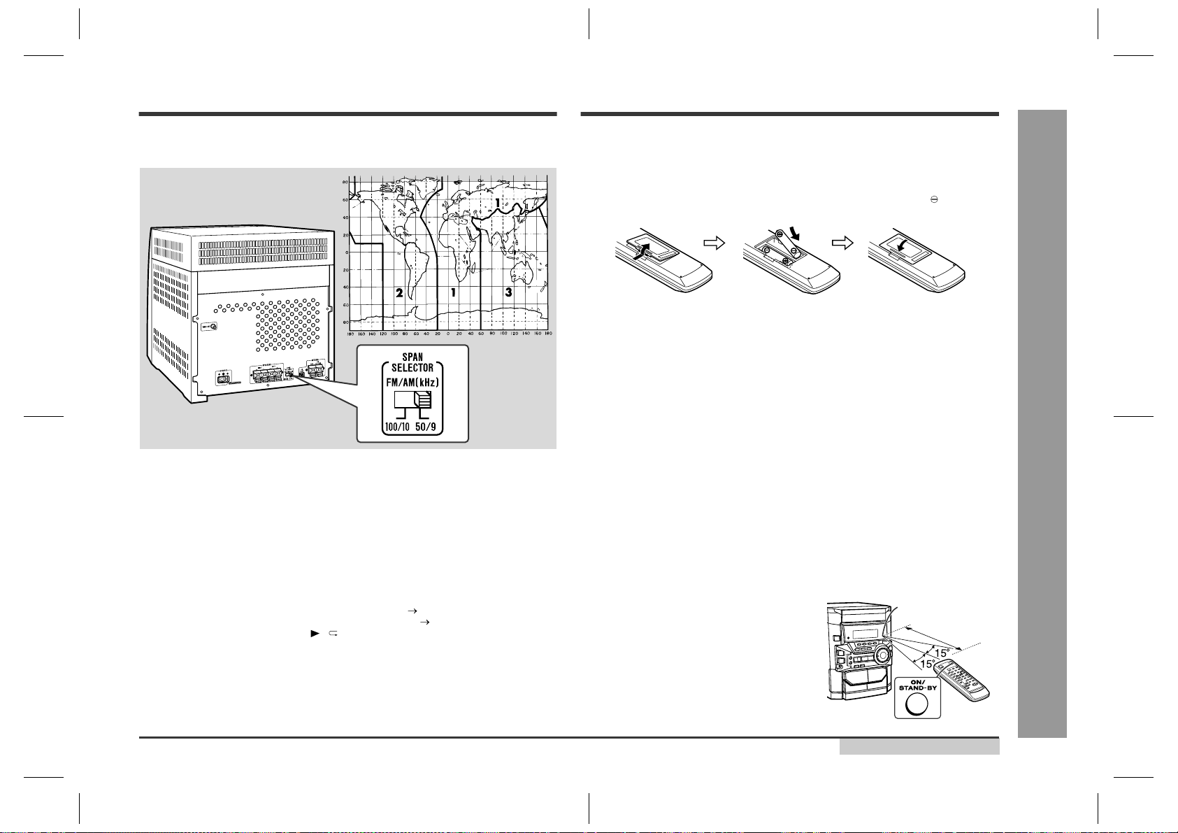
– 43 –
CD-BK110V/CD-BP99V
VOLTAGE
4.86 V
0 V
4.85 V
0 V
4.78 V
4.82 V
4.84 V
0 V
4.91 V
4.72 V
2.34 V
2.31 V
0 V
0 V
4.91 V
4.88 V
4.88 V
0 V
4.91 V
0 V
0 V
0 V
0 V
4.95 V
0 V
0.37 V
0 V
0 V
0 V
0 V
4.97 V
4.97 V
4.97 V
4.87 V
4.98 V
4.97 V
0 V
0 V
4.83 V
0 V
1.94 V
13.76 V
13.76 V
13.76 V
3.55 V
4.85 V
4.85 V
4.72 V
4.97 V
0 V
9
8
7
6
5
4
3
2
1
30
29
28
27
26
25
24
23
22
21
20
19
18
17
16
15
14
13
12
11
10
40
39
38
37
36
35
34
33
32
31
PIN
NO.
VOLTAGE
IC701
0 V
0 V
4.97 V
4.97 V
4.97 V
4.97 V
0 V
0 V
–29.7 V
–29.5 V
–29.5 V
–29.5 V
–29.5 V
–29.5 V
–29.5 V
–29.5 V
–29.5 V
–29.5 V
–29.5 V
–29.5 V
–26.4 V
–20.2 V
–26.4 V
–29.5 V
–20.2 V
–20.2 V
–29.5 V
–26.4 V
–29.5 V
–29.5 V
–20.2 V
–17.3 V
–29.5 V
–29.5 V
–29.5 V
–29.5 V
–26.4 V
–20.2 V
–23.3 V
–29.5 V
–29.5 V
–26.4 V
–26.4 V
–26.4 V
–26.4 V
–26.4 V
–26.4 V
–26.4 V
–26.4 V
–26.4 V
PIN
NO.
VOLTAGE
51
64
63
65
66
67
68
69
70
71
72
73
74
75
76
77
78
79
80
62
61
60
59
58
57
56
55
54
53
52
85
84
86
87
88
89
90
83
82
81
50
49
48
47
46
45
44
43
42
41
95
94
96
97
98
99
100
93
92
91
0 V
0 V
0 V
4.96 V
4.96 V
4.96 V
4.96 V
4.89 V
4.78 V
4.78 V
4.78 V
4.78 V
4.78 V
4.78 V
4.78 V
4.78 V
5.1 V
5.5 V
5.0 V
4.66 V
5.03 V
4.97 V
10.0 V
0 V
9
8
7
6
5
4
3
2
1
24
23
22
21
20
19
18
17
16
15
14
13
12
11
10
PIN
NO.
VOLTAGE
IC601
0 V
0 V
0.55 V
2.16 V
0 V
1.25 V
0 V
0.58 V
3.17 V
3.55 V
0 V
0 V
4.72 V
4.37 V
0 V
3.67 V
0.38 V
0 V
0 V
0 V
2.16 V
0.55 V
0 V
0 V
9
8
7
6
5
4
3
2
1
24
23
22
21
20
19
18
17
16
15
14
13
12
11
10
PIN
NO.
VOLTAGE
IC101
2.12 V
4.78 V
2.12 V
2.11 V
0 V
4.65 V
4.65 V
3.02 V
4.78 V
4.08 V
1.63 V
1.13 V
2.08 V
1.31 V
1.29 V
2.07 V
0 V
1.43 V
1.99 V
1.44 V
2.08 V
2.08 V
4.48 V
3.35 V
9
8
7
6
5
4
3
2
1
24
23
22
21
20
19
18
17
16
15
14
13
12
11
10
PIN
NO.
VOLTAGE
IC303
2.15 V
0 V
0 V
0 V
0 V
4.83 V
9.87 V
4.4 V
0 V
0 V
4.64 V
2.27 V
4.66 V
0 V
2.13 V
0 V
4.86 V
0.73 V
0.73 V
6.3 V
0 V
2.33 V
9
8
7
6
5
4
3
2
1
22
21
20
19
18
17
16
15
14
13
12
11
10
PIN
NO.
VOLTAGE
IC302
0 V
0 V
16.72 V
0 V
0 V
0 V
16.72 V
0 V
0 V
34.2 V
16.6 V
0 V
9
8
7
6
5
4
3
2
1
12
11
10
PIN
NO.
VOLTAGE
IC901
(CD-BK110V)
3
2
1
PIN
NO.
VOLTAGE
IC902
20.3 V
0 V
9.97 V
3
2
1
PIN
NO.
VOLTAGE
IC904
20.3 V
0.67 V
5.7 V
3
2
1
PIN
NO.
VOLTAGE
Q905
14.33 V
20.3 V
13.8 V
8
9
7
6
5
4
3
2
1
PIN
NO.
VOLTAGE
IC301
0.8 V (0V)
1.5 V (0V)
3.6 V (0.4V)
1.5 V (0V)
0 V (0V)
3.6 V (0.4V)
2.8 V (0.2V)
3.5 V (0.3V)
3.6 V (0.3V)
19.35 V
0 V
0 V
0 V
0 V
0 V
0.28 V
0 V
0 V
0 V
0 V
0 V
9
8
7
6
5
4
3
2
1
12
11
10
PIN
NO.
VOLTAGE
IC901
(CD-BP99V)
3
2
1
PIN
NO.
VOLTAGE
IC704
5 V
0 V
5 V
1.5V
1.0V
3.3V
1.3V
5.0V
5.0V
3.3V
3.3V
1.5V
0V
0V
3.3V
3.3V
3.3V
0V
3.3V
3.3V
3.3V
3.3V
3.3V
3.3V
1.3V
3.3V
0V
0.5V
2.2V
3.5V
0V
5.0V
0V
0V
2.5V
2.0V
2.5V
0V
0V
3.3V
0V
1.5V
1.5V
9
8
7
6
5
4
3
2
1
30
29
28
27
26
25
24
23
22
21
20
19
18
17
16
15
14
13
12
11
10
40
39
38
37
36
35
34
33
32
31
PIN
NO. NO.
VOLTAGE
ICV2
PIN
VOLTAGE
0V
0.5V
2.5V
3.3V
3.3V
0V
0V
0V
0V
0V
0V
0V
0V
0V
0V
0V
0V
0V
3.3V
0V
3.3V
0V
0V
0V
60
59
58
57
56
55
54
53
52
51
61
74
73
72
71
70
69
68
67
66
65
64
63
62
0V
0V
0V
0V
1.5V
2.3V
3.3V
0V
1.5V
0V
0V
0V
3.3V
2.2V
3.3V
1.0V
78
77
76
75
79
90
89
88
87
86
85
84
83
82
81
0V
1.5V
1.5V
0V
2.2V
2.5V
1.0V
0.3V
0.5V
2.6V
50
49
48
47
46
45
44
43
42
41
0V
1.5V
2.5V
2.5V
0V
0V
0V
2.3V
0V
3.0V
100
99
98
97
96
95
94
93
92
91
80
0V
0V
0V
0V
0.5V
0V
0V
0V
0V
0.1V
5.0V
0V
0V
1.5V
3.0V
0V
0V
5.0V
0V
0V
0.1V
5.0V
0V
0V
5.0V
0V
0V
0V
0V
0V
0V
0V
9
8
7
6
5
4
3
2
1
30
29
28
27
26
25
24
23
22
21
20
19
18
17
16
15
14
13
12
11
10
32
31
PIN
NO. NO.
VOLTAGE
ICV1
PIN
VOLTAGE
5.0V
5.0V
5.0V
5.0V
0V
3.0V
5.0V
0V
5.0V
0V
0V
0V
0V
0V
3.0V
0V
0V
5.0V
0V
0V
0V
0V
0.1V
1.2V
42
41
40
39
38
37
36
35
34
33
43
56
55
54
53
52
51
50
49
48
47
46
45
44
3.3V
3.3V
3.3V
3.3V
3.3V
0V
3.3V
2.8V
60
59
58
57
61
64
63
62
1.9V
4.9V
0V
0V
1.6V
1.6V
2.1V
0V
0V
0V
0V
0V
2.1V
2.1V
2.1V
1.6V
1.6V
1.8V
2.1V
0V
0V
2.1V
4.9V
3.5V
4.9V
1.6V
2.1V
2.1V
0V
0V
0V
0V
0V
0V
0V
4.2V
9
8
7
6
5
4
3
2
1
30
29
28
27
26
25
24
23
22
21
20
19
18
17
16
15
14
13
12
11
10
36
35
34
33
32
31
0V
2.1V
2.1V
4.9V
2.1V
41
2.1V
42
40
39
38
37
PIN
NO.
VOLTAGE
IC3
2.5V
1.5V
1.5V
0V
3.0V
0.5V
0.5V
2.6V
0V
0V
0.5V
0V
0V
5.0V
0V
3.0V
0V
0V
0V
0V
3.3V
0V
1.0V
2.7V
1.6V
1.5V
1.5V
0V
2.5V
0V
0V
0V
0V
0V
0V
0V
9
8
7
6
5
4
3
2
1
30
29
28
27
26
25
24
23
22
21
20
19
18
17
16
15
14
13
12
11
10
36
35
34
33
32
31
0V
0V
0.3V
0V
40
39
38
37
PIN
NO.
VOLTAGE
ICV3
5.0V
2.2V
2.0V
0V
3.0V
2.0V
2.2V
2.2V
8
7
6
5
4
3
2
1
PIN
NO.
VOLTAGE
ICV4
0V
3.0V
3.3V
3.3V
0V
0V
0V
1.6V
1.6V
1.6V
1.6V
1.6V
1.6V
1.6V
1.7V
4.7V
0V
1.6V
0V
2.4V
3.3V
0V
1.6V
3.0V
0V
3.3V
0V
0.7V
0V
0V
0V
0V
0V
1.6V
3.3V
0V
1.6V
1.6V
1.6V
1.6V
0V
2.1V
2.1V
0V
3.3V
3.5V
3.3V
3.3V
3.3V
1.6V
1.6V
1.5V
0V
1.5V
3.0V
3.3V
1.8V
3.0V
0V
0V
0V
1.7V
2.4V
0V
9
8
7
6
5
4
3
2
1
30
29
28
27
26
25
24
23
22
21
20
19
18
17
16
15
14
13
12
11
10
50
49
48
47
46
45
44
43
42
41
40
39
38
37
36
35
34
33
32
31
PIN
NO.
VOLTAGE
51
64
63
62
61
60
59
58
57
56
55
54
53
52
3.4V
0V
0V
3.2V
0V
0V
0V
0V
0V
4.8V
4.9V
4.9V
4.6V
0V
4.9V
0V
68
67
66
65
69
80
79
78
77
76
75
74
73
72
71
70
IC2
1.6V
0V
1.6V
1.6V
1.6V
0V
0V
1.6V
3.3V
0V
0V
0V
0V
1.6V
1.6V
1.6V
1.6V
1.6V
1.6V
2.6V
1.6V
1.6V
1.6V
1.6V
1.6V
0V
0V
0V
1.6V
3.3V
9
8
7
6
5
4
3
2
1
30
29
28
27
26
25
24
23
22
21
20
19
18
17
16
15
14
13
12
11
10
PIN
NO.
VOLTAGE
IC1
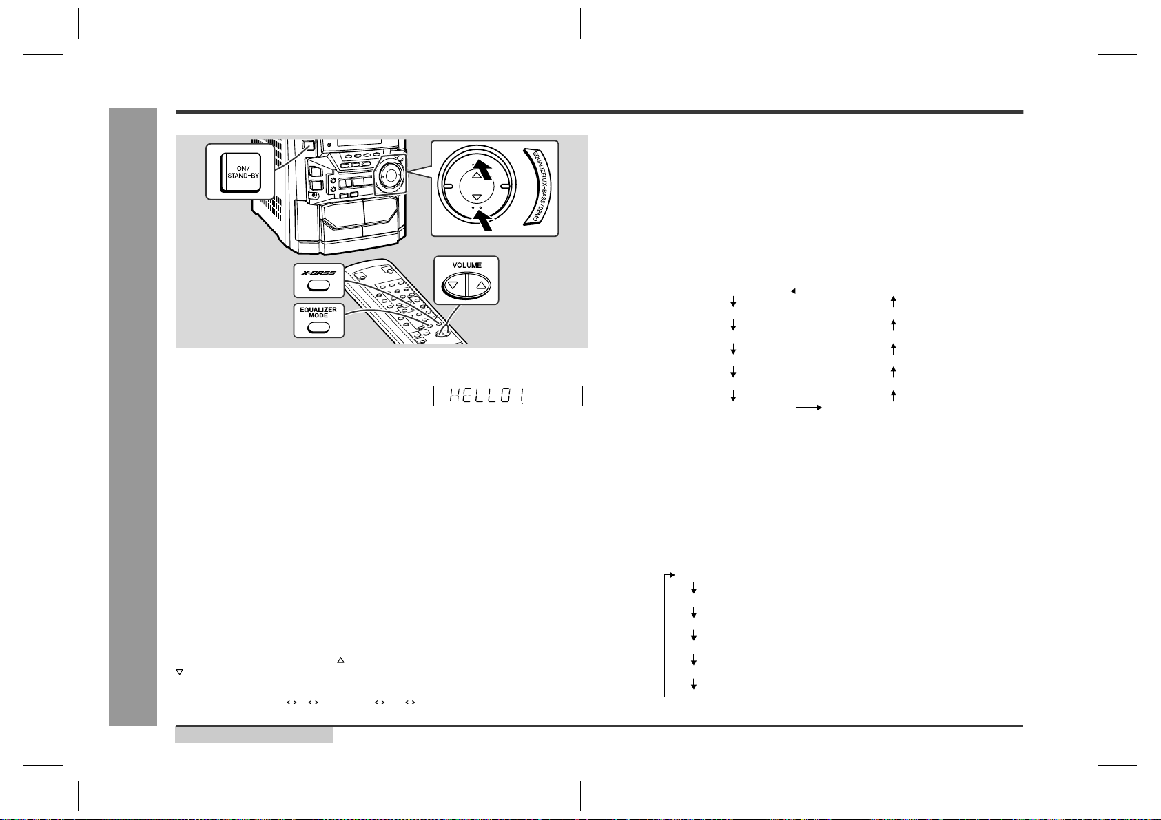
CD-BK110V/CD-BP99V
– 44 –
WAVEFORMS OF CD CIRCUIT
T
FDO
TDO
Stopped
CH1=500 mV
DC 10:1
CH3=500 mV
DC 10:1
500 ms/div
(500 ms/div)
NORM:20 kS/s
1
3
=Record Length=
Smoothing : ON CH1 : 0.000 V
CH2 : 0.0 V
Main : 100 K
Zoom : 2 K
Mode : AUTO
Type : EDGE CH1
Delay : 0.0 ns
Hold off : 0.2 µs
CH3 : 0.000 V
CH4 : 0.00 V
BW : FULL
=Trigger==Filter= =Offset=
CH1
v/DIV
500 mV
1
IC2 24
2
IC2 23
T
FDO
DRF
TE
Stopped
CH1=500 mV
DC 10:1
CH2=10 V
DC 10:1
CH3=1 V
DC 10:1
500 ms/div
(500 ms/div)
NORM:20 kS/s
1
2
3
=Record Length=
Smoothing : ON CH1 : 0.000 V
CH2 : 0.0 V
Main : 100 K
Zoom : 2 K
Mode : AUTO
Type : EDGE CH1
Delay : 0.0 ns
Hold off : 0.2 µs
CH3 : 0.00 V
CH4 : 0.00 V
BW : FULL
=Trigger==Filter= =Offset=
-3 div -1 div 0 div +1 div +3 div
CH Position To
CH2
Position
0.20 div
1
IC2 24
3
IC2 72
4
IC1 18 ,
IC2 16
Vp-p=1.0 V~1.3 V
0.5 mV/div,0.5 µsec/div
5
IC1 27
T
T
TE
DRF
Stopped
CH1=10 V
DC 10:1
CH2=1 V
DC 10:1
100 ms/div
(100 ms/div)
NORM:100 kS/s
2
1
=Record Length=
Smoothing : ON CH1 : 0.0 V
CH2 : 0.00 V
Main : 100 K
Zoom : 2 K
Mode : NORMAL
Type : EDGE CH1
Delay : 2.924 ms
Hold off : 0.2 µs
CH3 : 0.00 V
CH4 : 0.00 V
BW : FULL
=Trigger=
=Filter= =Offset=
3
IC2 72
4
IC1 18 ,
IC2 16
T
T
FDO
SPDO
Stopped
CH1=200 mV
DC 10:1
CH2=500 mV
DC 10:1
500 ms/div
1999/04/07 09:51:15
(500 ms/div)
NORM:20 kS/s
2
1
=Record Length=
Smoothing : ON CH1 : 0.000 V
CH2 : 0.000 V
Main : 100 K
Zoom : 2 K
Mode : NORMAL
Type : EDGE CH2
Delay : 2.924 ms
Hold off : 0.2 µs
CH3 : 0.00 V
CH4 : 0.00 V
BW : FULL
=Trigger==Filter= =Offset=
1
IC2 24
6
IC2 25
T
FDO
PDO2
PDO1
Stopped
CH1=500 mV
DC 10:1
CH3=1 V
DC 10:1
CH4=1 V
DC 10:1
500 ms/div
(500 ms/div)
NORM:20 kS/s
1
4
3
=Record Length=
Smoothing : ON CH1 : 0.000 V
CH2 : 0.0 V
Main : 100 K
Zoom : 2 K
Mode : AUTO
Type : EDGE CH2
Delay : 0.0 ns
Hold off : 0.2 µs
CH3 : 0.00 V
CH4 : 0.00 V
BW : FULL
=Trigger==Filter= =Offset=
CH1
v/DIV
500 mV
1999/04/05 17:33:17
1
IC2 24
7
IC2 1
8
IC2 2
T
T
DOUT
Stopped
CH1=2 V
DC 10:1
500 ns/div
1999/04/07 09:25:28
(500 ns/div)
NORM:200 MS/s
1
=Record Length=
Smoothing : ON CH1 : 0.00 V
CH2 : 0.00 V
Main : 1 K
Zoom : 100
Mode : NORMAL
Type : EDGE CH1
Delay : 2.887 ms
Hold off : 0.2 µs
CH3 : 0.00 V
CH4 : 0.00 V
BW : FULL
=Trigger=
=Filter= =Offset=
9
IC2 37
T
T
DATA
DATACK
LRSY
Stopped
CH1=2 V
DC 10:1
CH2=2 V
DC 10:1
CH3=2 V
DC 10:1
5 us/div
(5 us/div)
NORM:100 kS/s
1
2
3
=Record Length=
Smoothing : ON CH1 : 0.00 V
CH2 : 0.00 V
Main : 5 K
Zoom : 100
Mode : AUTO
Type : EDGE CH3
Delay : 0.0 ns
Hold off : 0.2 µs
CH3 : 0.00 V
CH4 : 0.00 V
BW : FULL
=Trigger==Filter= =Offset=
CH3
v/DIV
2 V
1999/04/05 20:50:17
10
IC2 57
IC2 58
IC2 59
11
12
T
T
EFBL
FDO
TE
Stopped
1
2
3
=Record Length=
Smoothing : ON CH1 : 0.000 V
CH2 : 0.000 V
Main : 100 K
Zoom : 2 k
Mode : SINGLE
Type : EDGE CH1
Delay : 0.0 ns
Hold off : 0.2 µs
CH3 : 0.00 V
CH4 : 0.00 V
BW : FULL
=Trigger==Filter= =Offset=
CH2
v/DIV
200 mV
1999/04/05 20:26:47
1
IC2 24
4
IC1 18 ,
IC2 16
IC1 13 ,
IC2 22
13
CH1=500 mV
DC 10:1
CH2=200 mV
DC 10:1
CH3=1 V
DC 10:1
500 ms/div
(500 ms/div)
NORM:20 kS/s
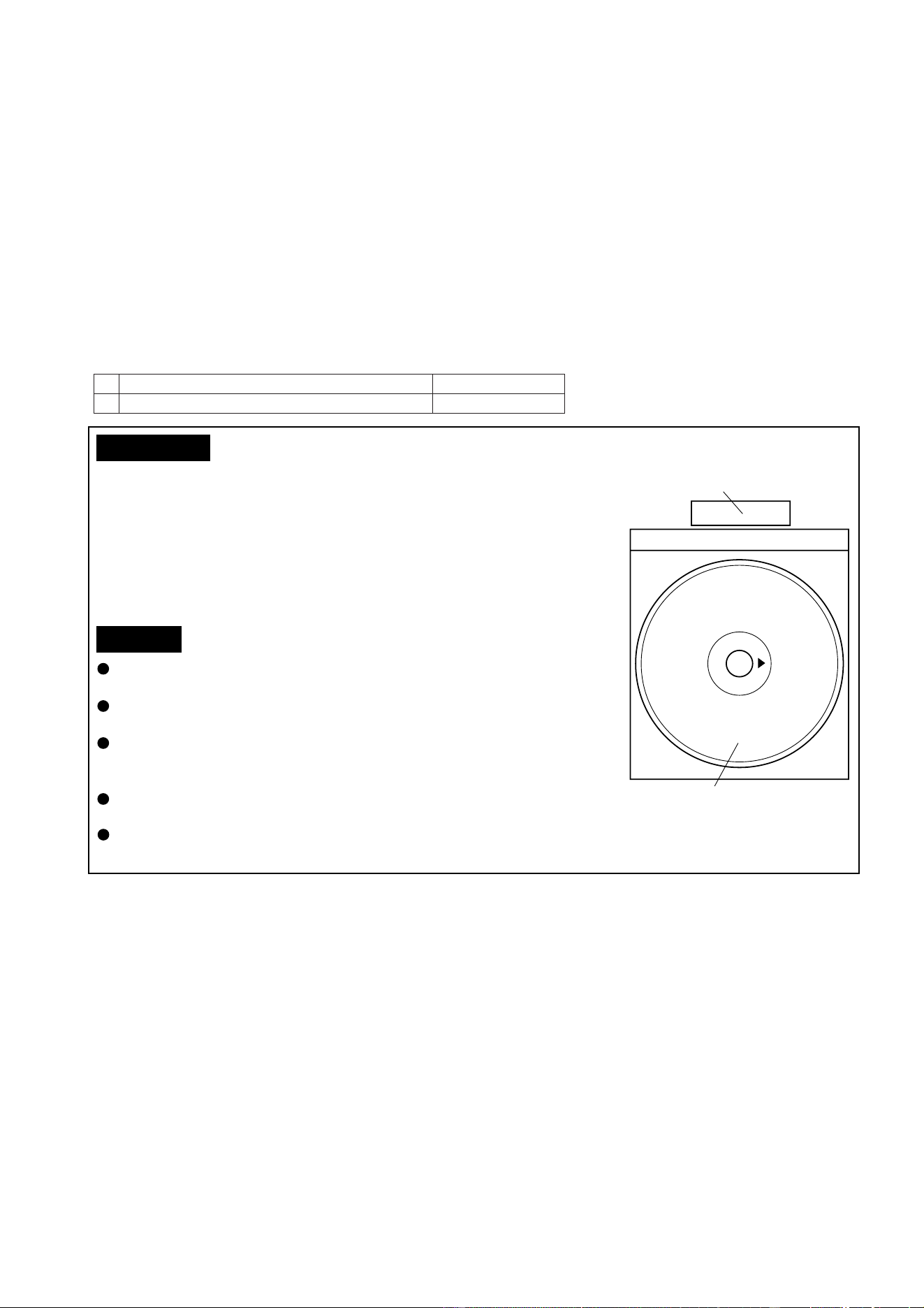
– 45 –
CD-BK110V/CD-BP99V
Parts code
1. CD optical pickup Lens cleaner disc UDSKA0004AFZZ
HOW TO USE
CAUTION
Cleaning fluid
Cleaner disc
Using the brush in the cleaner cap, apply 1 or 2 drops of the cleaning fluid to the
brush on the CD cleaner disc which has the mark next to it.
Place the CD cleaner disc onto the CD disc tray with the brush side down,then
press the play button.
You will hear music for about 20 seconds and the CD player will automatically stop.
If it continuous to turn, press the stop button.
1.
2.
3.
The CD lens cleaner should be effective for 30-50 operations, however if the
brushes become worn out earlier then please the cleaner disc.
If the CD cleaner brushes become very wet then wipe off any excess fluid with a soft
cloth.
Do not drink the cleaner fluid or allow it to come in contact with the eyes. In the
event of this happening then drink and / or rinse with clean water and seek medical
advice.
The CD cleaner disc must not be used on car CD players or on computer CD-ROM
drives.
All rights reserved. Unauthorized duplicating, broadcasting and renting this product
is prohibited by law.
TROUBLESHOOTING
When the CD does not function
When the CD section does not operate when the objective lens of the optical pickup is dirty, this section may not operate. Clean
the objective lens, and check the playback operation. When this section does not operate even after the above step is taken, check
the following items.
Remove the cabinet and follow the trouble shooting instructions.
"Track skipping and/or no TOC (Table Of Contents) may be caused by build up of dust other foreign matter on the laser pickup
lens. Before attempting any adjustment make certain that the lens is clean. If not, clean it as mentioned below."
Turn off the power, and wipe the lens softly using a cleaning paper moistened with commercially available cleaning solution so
as not to damage it. Be careful not to touch the lens with bare hands.
Dust gradually accumulates on the objective lens during use, and it may degrade performance. To avoid this problem, use a
cleaning disc designed for CD optical pickup lenses.
When a CD cannot be played
1. "E-CD01" is displayed.
(1) Check the power to IC2 (LC78636E), the presence of the clock signal (16.943 MHz) and the status of the RESET terminal
(pin 71 on IC2).
(2) Does the pickup move to the PICKUP-IN Switch (SW4) position ?
If (1) and (2) are OK, check the system microcomputer (especially the communication line with the DSP).
2. Pressing the CD operation key is accepted, but playback does not occur.
(1) Focus-HF system check
(2) Tracking system check
(3) Spin system check
(4) PLL system check
(5) Others
CD-BK110V/CD-BP99V
– 46 –
Vp-p=1.0 V~1.3 V
0.5 mV/div,0.5 µsec/div
T
FDO
DRF
TE
Stopped
CH1=500 mV
DC 10:1
CH2=10 V
DC 10:1
CH3=1 V
DC 10:1
500 ms/div
(500 ms/div)
NORM:20 kS/s
1
2
3
=Record Length=
Smoothing : ON CH1 : 0.000 V
CH2 : 0.0 V
Main : 100 K
Zoom : 2 K
Mode : AUTO
Type : EDGE CH1
Delay : 0.0 ns
Hold off : 0.2 µs
CH3 : 0.00 V
CH4 : 0.00 V
BW : FULL
=Trigger==Filter= =Offset=
-3 div -1 div 0 div +1 div +3 div
CH Position To
CH2
Position
0.20 div
T
FDO
TDO
Stopped
CH1=500 mV
DC 10:1
CH3=500 mV
DC 10:1
500 ms/div
(500 ms/div)
NORM:20 kS/s
1
3
=Record Length=
Smoothing : ON CH1 : 0.000 V
CH2 : 0.0 V
Main : 100 K
Zoom : 2 K
Mode : AUTO
Type : EDGE CH1
Delay : 0.0 ns
Hold off : 0.2 µs
CH3 : 0.000 V
CH4 : 0.00 V
BW : FULL
=Trigger==Filter= =Offset=
CH1
v/DIV
500 mV
If the level is not normal, check around pins 27~29 on IC1.
1. Is focus servo activated ?
(Waveform drawing Figure 46-2)
Pins 1~11 on IC1
Check the laser diode driver Q3 peripheral circuit.
Focus error circuit (pins 20 and 21 on IC1).
When a disc is loaded, start playback operation.
2. Does DRF change from "L" to "H" ?
Is the disc rotating ?
3. Is the HF waveform normal ?
(Waveform drawing Figure 46-3)
Check the spin system.
If the disc is spinning and a HF waveform is generated,
DRF will go H.
Figure 46-1
Check the laser diode driver Q3 peripheral circuit.
(1) Focus-HF system check.
Although a CD is inserted and the cover is closed, "NO
DISC" is displayed.
1. Does the pickup move to the PICKUP-IN Switch (SW4)
position ?
Sled motor (M2).
Press the OPEN/CLOSE switch (SW1) without inserting a
disc, and try starting the playback operation.
2. Does the focus (lens) move up and down ?
(Waveform drawing Figure 46-1).
Check the focus peripheral circuit.
3. Is the laser lit ?
Spindle motor (M1).
4. Is the turntable rotating ?
Figure 46-2 Figure 46-3
Yes
Yes
Yes
No
No
No
No
No
No
No
Yes
Yes
No
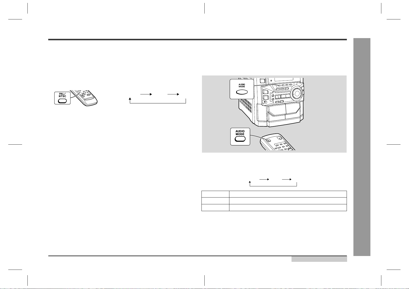
– 47 –
CD-BK110V/CD-BP99V
T
T
FDO
SPDO
Stopped
CH1=200 mV
DC 10:1
CH2=500 mV
DC 10:1
500 ms/div
1999/04/07 09:51:15
(500 ms/div)
NORM:20 kS/s
2
1
=Record Length=
Smoothing : ON CH1 : 0.000 V
CH2 : 0.000 V
Main : 100 K
Zoom : 2 K
Mode : NORMAL
Type : EDGE CH2
Delay : 2.924 ms
Hold off : 0.2 µs
CH3 : 0.00 V
CH4 : 0.00 V
BW : FULL
=Trigger==Filter= =Offset=
T
T
TE
DRF
Stopped
CH1=10 V
DC 10:1
CH2=1 V
DC 10:1
100 ms/div
(100 ms/div)
NORM:100 kS/s
2
1
=Record Length=
Smoothing : ON CH1 : 0.0 V
CH2 : 0.00 V
Main : 100 K
Zoom : 2 K
Mode : NORMAL
Type : EDGE CH1
Delay : 2.924 ms
Hold off : 0.2 µs
CH3 : 0.00 V
CH4 : 0.00 V
BW : FULL
=Trigger=
=Filter= =Offset=
The tracking servo is not activated.
Check the peripheral circuits at pins 18 and 19 on IC1, pin 16 on
IC2, and CNS1A/B.
If the waveform shown in Figure 47-1 appears and soon after
NO DISC appears ?
(2) Tracking system check.
Check the TE waveform at pin 18 on IC1.
A normal jump operation cannot be completed or the beginning of
the track cannot be found.
Check the around pin 23 on IC2.
"Initialization" is possible, but play is not possible ?
Data cannot be read. Check the VCO-PLL system.
"Initialization" is not possible.
Figure 47-1
Figure 47-2
Press the OPEN/CLOSE switch without inserting a disc, and
then try starting the play operation.
(3) Spin system check.
The spin driver circuit is OK.
1. The turntable rotates a little ?
(Waveform drawing Figure 47-2)
Check around pin 25 on IC2, pins 15 and 16 on IC3, and CNS3A/B.
2. The turntable doesn't rotate.
No
Yes
No
Yes
Yes
No
CD-BK110V/CD-BP99V
– 48 –
T
T
DOUT
Stopped
CH1=2 V
DC 10:1
500 ns/div
1999/04/07 09:25:28
(500 ns/div)
NORM:200 MS/s
1
=Record Length=
Smoothing : ON CH1 : 0.00 V
CH2 : 0.00 V
Main : 1 K
Zoom : 100
Mode : NORMAL
Type : EDGE CH1
Delay : 2.887 ms
Hold off : 0.2 µs
CH3 : 0.00 V
CH4 : 0.00 V
BW : FULL
=Trigger==Filter= =Offset=
T
FDO
PDO2
PDO1
Stopped
CH1=500 mV
DC 10:1
CH3=1 V
DC 10:1
CH4=1 V
DC 10:1
500 ms/div
(500 ms/div)
NORM:20 kS/s
1
4
3
=Record Length=
Smoothing : ON CH1 : 0.000 V
CH2 : 0.0 V
Main : 100 K
Zoom : 2 K
Mode : AUTO
Type : EDGE CH2
Delay : 0.0 ns
Hold off : 0.2 µs
CH3 : 0.00 V
CH4 : 0.00 V
BW : FULL
=Trigger==Filter= =Offset=
CH1
v/DIV
500 mV
1999/04/05 17:33:17
Is pin 35 (C2F) on IC2 "L" ?
Yes
No
The HF waveform is normal and the time is displayed
normally, but no sound is produced. Or the sound
has dropouts.
(5) Others.
There are too many error flags on a damaged disc which
makes error correction impossible.
Check again using a known good disc.
1. When playing at normal speed.
Check the peripheral circuit at pin 37 (DOUT) on IC2 and
the waveform (Figure 48-2).
If OK, Check the unit.
When a disc is loaded, start play operation.
(4) PLL system check.
The HF waveform is normal, but the TOC data cannot be
read.
Check the PDO waveform. (Figure 48-1)
Check around pins 1~6 on IC2.
Figure 48-1
Figure 48-2

– 49 –
CD-BK110V/CD-BP99V
FUNCTION TABLE OF IC
IC2 VHiLC78636E-1 : Servo/Signal Control (LC78636E) (1/2)
1 PD01 Output — For PULL Phase-comparison output terminal for built-in VCO control.
2 PD02 Output Input Phase-comparison output terminal for built-in VCO control.
Rough servo : OFF, phase servo : ON.
3 VVSS — — Ground terminal for built-in VCO.
4 PCKIST Input — Resistor terminal for setting the PDO output current.
5 VVDD Input — Power terminal for built-in VCO.
6 FR Input — Resistor terminal for setting the VCO frequency range.
7 HFL Input — Mirror detection signal input terminal.
8 SLCIST Input — For slice level control
Resistance connection terminal for current adjustment of
SLCO output.
9 SLCO Output — Control output.
10 EFMIN Input — EFM signal input terminal.
11* JITTV Output Unfixed Jitter detection/monitor terminal.
12 JITTC Output — Jitter detection/adjustment terminal.
13 BH Input — BH signal input terminal. A/D input.
14 PH(RFENV) Input — PH signal or RFENV signal input terminal. A/D input.
15 FE Input — FE signal input terminal. A/D input.
16 TE Input — TE signal input terminal. A/D input.
17 VREF Input — VREF signal input terminal. A/D input.
18 ADAVDD Input — AD for servo, D/A power terminal.
19 ADAVSS — — AD for servo, D/A ground terminal.
20* PHREF Output (1/2VDD) PH reference output terminal. D/A output.
21* BHREF Output (1/2VDD) BH reference output terminal. D/A output.
22 TBLO Output (1/2VDD) Output terminal for tracking balance. D/A output.
23 TDO Output (1/2VDD) Output terminal for tracking control. D/A output.
24 FDO Output (1/2VDD) Output terminal for focus control. D/A output.
25 SPDO Output (1/2VDD) Output terminal for spindle control. D/A output.
26 SLDO Output (1/2VDD) Output terminal for sled control. D/A output.
27* FG Input — FG signal input terminal. (When not used, connect to 0 V)
28 LASER Output L LASER ON/OFF control terminal.
29 CONT1 Input/Output Input mode General purpose input/output terminal 1.
Controlled with serial data command
30 CONT2 Input/Output Input mode General purpose input/output terminal 2.
from microcomputer
.
When not used,
31 CONT3 Input/Output Input mode General purpose input/output terminal 3.
set it as the input terminal
and
32 CONT4 Input/Output Input mode General purpose input/output terminal 4.
open it by connecting
to 0 V, or set it
33 CONT5 Input/Output Input mode General purpose input/output terminal 5.
as the output terminal and open it.
34* PCK Output H Clock monitor terminal for EFM data replay. 4.3218 MHz as phase clock.
35 C2F Output H C2 flag output terminal.
36 VDD Input — Power terminal of digital system.
37* DOUT Output L Output terminal of digital OUT. (EIAJ format)
38* FSX Output L
Output terminal of synchronous signal of 7.35 kHz divided from quartz oscillation.
39* EFLG Output L C1, C2 correct monitor terminal.
40 TEST Input — Input terminal for test. Surely connected to 0 V.
41 EMPH Input/Output Input mode
Emphasis terminal. After resetting, it is configured as an input terminal. It can be controlled
from the outside. It is also becomes a emphasis monitor terminal under command control.
42* MUTEL Output H Mute output terminal for L channel.
43* MUTER Output H Mute output terminal for R channel.
Pin No.
Function
Terminal Name
Input/Output
Setting in Reset
In this unit, the terminal with asterisk mark (*) is open terminal which is not connected to the outside.

CD-BK110V/CD-BP99V
– 50 –
IC2 VHiLC78636E-1 : Servo/Signal Control (LC78636E) (2/2)
44 LVDD Input — L channel Power terminal for L channel.
45 LCHO Output 1/2VDD D/A converter L channel output terminal.
46 LVSS — — Ground terminal for L channel. Surely connected to 0 V.
47 RVSS — — R channel Ground terminal for R channel. Surely connected to 0 V.
48 RCHO Output 1/2VDD D/A converter R channel output terminal.
49 RVDD Input — Power terminal for R channel.
50 XVDD Input — For quartz Power terminal for quartz oscillation.
51 XIN Input Oscillation oscillation Ground terminal of 16.9344 MHz quartz oscillation.
52 XOUT Output Oscillation
53 XVSS — — Ground terminal for quartz oscillation. Surely connected to 0 V.
54 ASLRCK Input — For anti L/R clock input terminal. (When not used, connect to 0 V)
55 ASDACK Input — shock mode Bit clock input terminal. (When not used, connect to 0 V)
56 ASDFIN Input —
L/R channel data input terminal. (When not used, connect to 0 V)
57 LRSY Output L For digital L/R clock output terminal.
58 DATACK Output L data output Bit clock output terminal.
59 DATA Output L L/R channel data output terminal.
60 16M Output Clock output 16.9344 MHz output terminal.
61* SFSY Output L Output terminal of synchronous signal of subcode frame.
It drops when subcode stand by.
62* SBSY Output L Output terminal of synchronous signal of subcode block.
63* PW Output L Output terminal of sub codes P,A,R,S,T,U and W.
64 SBCK Input — Clock input terminal to read sub code. (When not used, connect to 0 V)
65 CE Input — For Chip enable signal input terminal.
66 CL Input —
microcomputer
Data transmission clock input terminal.
67 DI Input — interface Data input terminal.
68 DO Output L Data output terminal.
69 INT Output H Interruption signal output terminal.
70 WRQ Output H Interruption signal output terminal.
71 RES Input — Reset input terminal of LC78640. When turning on power, set it at "L".
72 DRF Output L Focus ON detection terminal.
73 VDD5V Input — Power terminal for microcomputer interface.
74 VSS — — Ground terminal of digital system. Surely connected to 0 V.
75 CONT6 Input/Output Input mode General purpose input/output terminal 6.
Controlled with serial data command
from microcomputer
.
When not used,
76 CONT7 Input/Output Input mode General purpose input/output terminal 7.
set it as the input terminal
and
open it by connecting
to 0 V, or set it
as the output terminal and open it.
77* V/P Output H Monitor output terminal for automatic switch of rough servo/phase control.
"H" for rough servo, and "L" for phase servo.
78* FSEQ Output L Output terminal synchronous signal detection. "H" is output when
synchronous signal detected by EFM signal matches synchronous signal
internally generated.
79* DEFECT Input/Output Input mode Defect terminal. After resetting, it is configured as an input terminal. It can be
controlled from the outside.
It also becomes a defect monitor terminal under command control
80* EFMO Output Unfixed EFM signal output terminal.
Pin No.
Function
Terminal Name
Input/Output
Setting in Reset
In this unit, the terminal with asterisk mark (*) is open terminal which is not connected to the outside.
Be sure to supply the same potential to each power terminal. (VVDD, ADAVDD, VDD, LVDD, RVDD, XVDD)
Terminal witch is controlled by the power terminal (VDD5 V) for a microcomputer interface :
CE (65 pin), CL (66 pin), DI (67 pin), DO (68 pin), INT (69 pin), WRQ (70 pin), RES (71 pin), DRF (72 pin),
CONT6 (75 pin), CONT7 (76 pin)
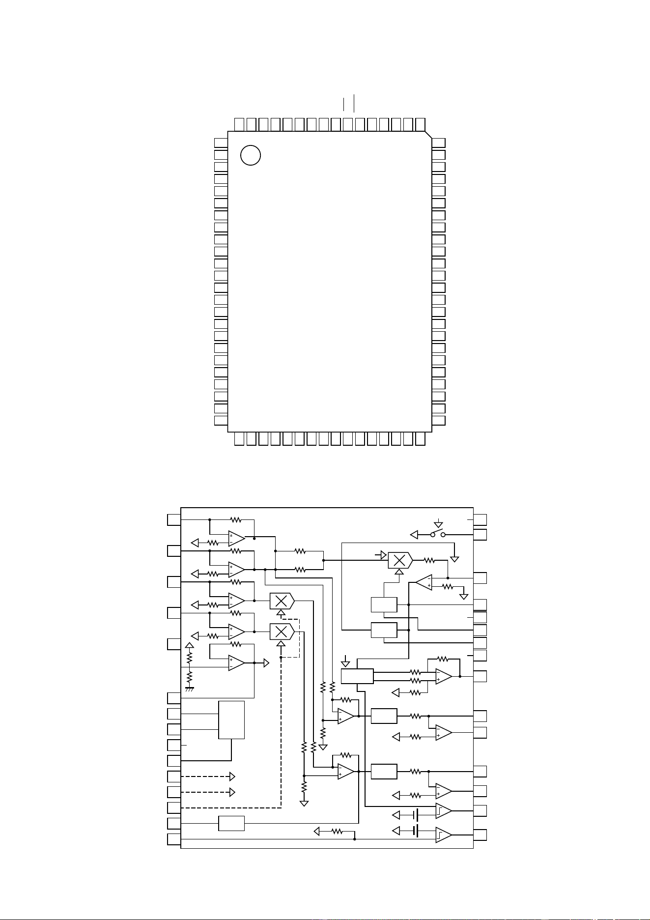
– 51 –
CD-BK110V/CD-BP99V
Figure 51 BLOCK DIAGRAM OF IC
IC2 VHiLC78636E-1 : Servo/Signal Control (LC78636E)
IC1 VHiLA9235M-1 : Servo Amp. (LA9235M)
1
PDO1
2
PDO2
3
VVSS
4
PCKIST
5
VVDD
6
FR
7
HFL
8
SLCIST
9
SLCO
10
EFMIN
11
JITTV
12
JITTC
13
BH
14
PH(RFENV)
15
FE
16
TE
25
SPDO
26
SLDO
27
FG
28
LASER
29
CONT1
30
CONT2
CONT3
CONT4
CONT5
31
32
33
34
PCK
35
C2F
36
VDD
37
DOUT
38
FSX
39
EFLG
40
TEST
EFMO
DEFECT
FSEQ
V/P
CONT7
CONT6
VSS
VDD 5V
DRF
RES
WRQ
INT
DO
DI
CL
CE
17
VREF
18
ADAVDD
19
ADAVSS
20
PHREF
21
BHREF
22
TBLO
23
TDO
24
FDO
SBCK
PW
SBSY
SFSY
16M
DATA
DATACK
LRSY
ASDACK
ASLRCK
ASDFIN
XVSS
XOUT
XIN
XVDD
RVDD
RCHO
RVSS
LVSS
LCHO
LVDD
MUTER
MUTEL
EMPH
80
79
78
77
76
75
74
73
72
71
70
69
68
67
66
65
64
63
62
61
61
59
58
57
56
55
54
53
52
51
50
49
48
47
46
45
44
43
42
41
LC78636E
REF
LA9235M
REF
REF
REF
REF
REF
REF
REF
REF
AGCON
ODRV
AGCON
ODRV
REF
REF
LPF
LPF
APC
ODRV
REF
REF
REF
REF
LPF
PH/BH
PH
BH
1 30FIN1 VCC
2
29
FIN2
RFSW
3TIN1
4
27
TIN2
RF
26 NC
25 PH
24 BH
23 NC
5REF1
15
16
TESI
14TESTO
13EFBL
12AGON
11ODRV
10LDOF
9GND
8LDD
7LDS
6VREF
TEST
17 HFL
18 TE
19 TE-
20 FE
21 FE-
22 RFEV
28 RF-
CD-BK110V/CD-BP99V
– 52 –
1 VDD VDD Input (+) Power supply.
2 P37 -20 dB ATT Output -20 dB Attenuator.
3 P36 NO USE Output GND
DSA_STB Input/Output DSA strube.
4 P35 T_BIAS Output Tape record bias.
5 P34 T_T1/T2 Output Tape T1/T2 change.
6 P33 REC/PLAY Output Tape record/play change.
7 P32 RES OUT Output CD DSP reset & mpeg microcomputer reset.
8 P31 DRF Input CD RF level detection.
9 P30 WRQ Input CD DSP write request.
10 RESET RESET Input RESET.
11 X2 X2 Output Main clock.
12 X1 X1 Input Main clock.
13 VPP/IC XVPP/IC — GND
14* XT2 XT2 — OPEN.
15 P04 SPN Input Tuner span change.
16 VDD VDD Input (+) Power supply.
17 P27 CD CLK Output CD DSP clock.
18 P26 CD DI Output CD DSP command.
19 P25 CD DO Input CD DSP code Q out.
20 P24 CD CE Output CD DSP CE output.
21 P23 CE Output CE output.
22 P22 CLK Output CLOCK output.
23 P21 DI Output DATA output.
24 P20 DO Input DATA input.
25 AVSS AVSS — Analog ground.
26 ANI7 O/C SW Input CD open/close switch.
DISC NO SW Input CD DISC number switch.
DSA_DATA Input/Output DS data input.
27 ANI6 NO USE Input GND
TUNER SM Input Tuner signal meter input.
DSA_ACK Input/Output DSA ACR.
28 ANI5 SPEANA 2 Input Speana data input 16 kHz.
29 ANI4 SPEANA 1 Input Speana data input 1 kHz.
30 ANI3 SPEANA 0 Input Speana data input 63 kHz.
31-33 ANI2-ANI0 KEY 2-KEY 0 Input KEY input.
34 AVDD AVDD Input Analog VDD.
35 AVREF AVREF Input Analog REF voltage.
36 INTP3 P_IN Input Power failure detect.
37* P02 JOG 1 Input JOG volume input 1.
38 P01 JOG 0 Input JOG volume input 0.
39 INTP0 REMOCON Input Remocon input.
40 VSS VSS — Ground voltage.
41 P74 SMUTE Output System mute control.
42 P73 T_SOL_B Output Tape 2 solenoid control.
43 P72 T_SOL_A Output Tape 1 solenoid control.
44 P71 T_MOTOR Output Tape motor control.
45 P70 TIMER LED Output Timer LED control.
46 VDD VDD Input (+) Power supply.
47* P127 AC RLY_CONT Output AC relay control.
48 P126 SP-RLY Output Speaker output relay control.
49 P125 SP_DET Input Speaker output detection.
IC701 RH-iX0338AWZZ : System Microcomputer (IX0338AW) (1/2)
Port Name
Terminal Name
Pin No.
Input/Output
Function
In this unit, the terminal with asterisk mark (*) is (open) terminal which is not connected to the outside.
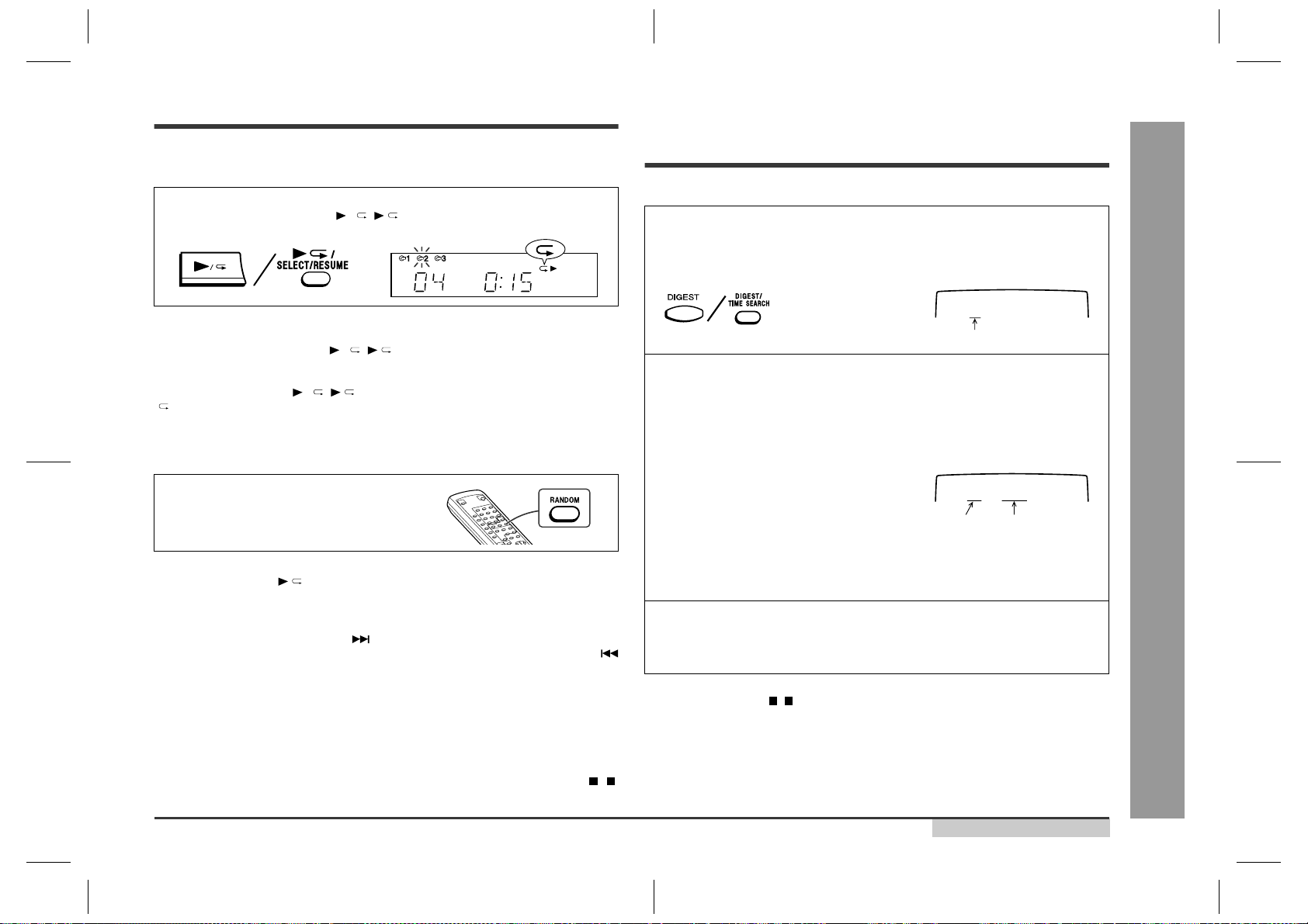
– 53 –
CD-BK110V/CD-BP99V
50 P124 T 1 RUN Input Tape 1 run pulse input.
51 P123 T 2 RUN Input Tape 2 run pulse input.
52 P122 CD CLAMP SW Input CD changer clamp switch.
53 P121 NO USE Input GND
54 P120 PLAY SW_B Input Play switch for T2.
55 P117 FPA Input Tape 2 A-Side full proof.
56 P116 FPB Input Tape 2 B-Side full proof.
57 P115 MIC SW Input Mic switch.
58* P114 LCK 0 Output LED driver lck.
59 P113
DISTOUT
Output Destination output.
60 FIP39 NO USE Output GND
61* FIP38 KARAOKE LATCH Output Karaoke latch.
62* FIP37 NO USE Output GND
MPEG_POW Output Mpeg power control.
63* FIP36 NO USE Output GND
RDS RST/ESS_ACK Output RDS fan reset.
64* FIP35 NO USE Input GND
RDS RDDA/ESS_STB Input RDS transmit data input/DSA strobe.
65* FIP34 NO USE Output GND
RDS RDCL/ESS_DI Output RDS clock/DSA data output.
66* FIP33 NO USE Input GND
RDS READY/ESS_DO Input RDS ready/DSA data input.
67* P103 DIST3 Input Destination input.
FIP32 P22 Output FL display driver.
68* P102 DIST2 Input Destination input.
FIP31 P21 Output FL display driver.
69 P101 DIST1 Input Destination input.
FIP30 P20 Output FL display driver.
70* P100 DIST0 Input Destination input.
FIP29 P19 Output FL display driver.
71-78 FIP28-FIP21 P18-P11 Output FL display driver.
79 VLOAD VLOAD Input FL driver (-) power supp. -30 V
80-89 FIP20-FIP11 P10-P1 Output FL display driver.
90-100 FIP10-FIP0 G11-G1 Output FL display driver.
IC701 RH-iX0338AWZZ : System Microcomputer (IX0338AW) (2/2)
Port Name
Terminal Name
Pin No.
Input/Output
Function
In this unit, the terminal with asterisk mark (*) is (open) terminal which is not connected to the outside.
CD-BK110V/CD-BP99V
– 54 –
IC601 VHiLC75341/-1 : Audio Processor (LC75341)
Figure 54 BLOCK DIAGRAM OF IC
19
20
21
222324
123
4
5
6
7
8
9
10 11 12 13 14 15 16
18
17
LVref
RVref
CONTROL
CIRCUIT
CONTROL
CIRCUIT
CONTROL
CIRCUIT
LOUT
LBASS
LIN
LSEL0
L4
L3
L2 L1
R1 R2
R3 R4
RSEL0
R1N
RTRELTRE
RBASS
ROUT
VREF
VDD
CLK
DI
CE
VSS
CCB
INTERFACE
CD
Tuner
Tape
Video
24 23 22 21 20 19 18 17 16 15 14 13
123456789101112
LC75341
DI
CE
VSS
LOUT
LBASS
LTRE
LIN
LSEL0
L4
L3
L2
L1
CLK
VDD
VREF
ROUT
RBASS
RTRB
RIN
RSEL0
R4
R3
R2
R1
– 55 –
CD-BK110V/CD-BP99V
1 TO CH2 inverted input.
2 FD CH1 inverted input.
3* FO CH1 output offset control.
4 FO+ CH1 inverted output.
5 FO- CH1 non-inverted output.
6 TR+ CH2 inverted output.
7 TR- CH2 non-inverted output.
8-14 GND GND
15 SL- CH3 non-inverted output.
16 SL+ CH3 inverted output.
17 SLDO CH3 inverted input.
18 VCC1 Power supply 1 (CH1, CH2, CH3)
19 STANDBY STANDBY signal input.
20 VRFE CH1-CH4 Reference voltage input.
21 MUTE Mute signal input (CH6).
22 IN5- CH5 inverted input.
23 IN5+ CH5 non-inverted input.
24 VCC2 Power supply 2 (CH4).
25 SPO SPDO CH4 inverted input.
26 SP+ CH4 inverted output.
27 SP- CH4 non-inverted output.
28 VCC3 Power supply 3 (CH5).
29-35 GND GND
36* OUT5+ CH5 non-inverted output.
37* OUT5- CH5 inverted output.
38 LOADING M- CH6 non-inverted output.
39
LOADING M+
CH6 inverted output.
40 VCC4 Power supply 4 (CH6).
41 LD_M- CH6 inverted input.
42 LD_M+ CH6 non-inverted input.
IC3 VHiM63001FP-1 : Focus/Tracking/Spin/Sled Driver (M63001FP)
Pin No.
Terminal
Name
Function
Figure 55-1 BLOCK DIAGRAM OF IC
In this unit, the terminal with asterisk mark (*) is open terminal
which is not connected to the outside.
1
2
3
4
5
6
7
8
9
10
11
12
13
14
15
16
17
18
19
20
21
28
29
30
31
32
33
34
35
36
37
38
39
40
41
42
27
26
25
24
23
22
TO
FD
FO
FO+
FO–
TR+
TR–
SL–
SL+
SLDO
VCC1
STANDBY
VTEF
MUTE
GND
GND
VCC3
SP–
SP+
SPO SPDO
VCC2(SPN)
IN5+
IN5–
LD_M+
LD_M–
VCC4
LOADING M+
LOADING M–
OUT5–
OUT5+
M63001FP
Pin No.
Terminal Name
Function
1 Clamp input terminal Input of 1.9 V clamp, 1 Vp-p composite or Y-signal.
2 GND Ground
3 Sag correction terminal Able to obtain an output without any sag by feeding back the sag, generated from output
coupling C, using the external C (see block diagram).
When not using the sag correction terminal, connect directly to the pin 4.
4,5 Output terminal 6 dB amplifier output. Able to drive 75 ohms video line.
6 Sag correction terminal Able to obtain an output without any sag by feeding back the sag, generated from output
coupling C, using the external C (see block diagram).
When not using the sag correction terminal, connect directly to the pin 5.
7 V+ Power source.
8 Clamp input terminal Input of 1.9 V clamp, 1 Vp-p composite or Y-signal.
ICV4 VHiNJM2267M-1 : Video Operation Amp. (NJM2267M)
6dB
Amp
6dB
Amp
75ohm
Driver
75ohm
Driver
Vout2
75
2.2
2.0k
Vout1
75
V5AG2
V5AG1
GND
2.2k
2.0k
Clamp
Clamp
7
5
6
4
3
2
1
8
VIN2
VOUT2
(6dB)
VOUT2
VOUT1
(6dB)
VOUT1
V+
VIN1
Correction terminal
Correction terminal
Figure 55-2 BLOCK DIAGRAM OF IC
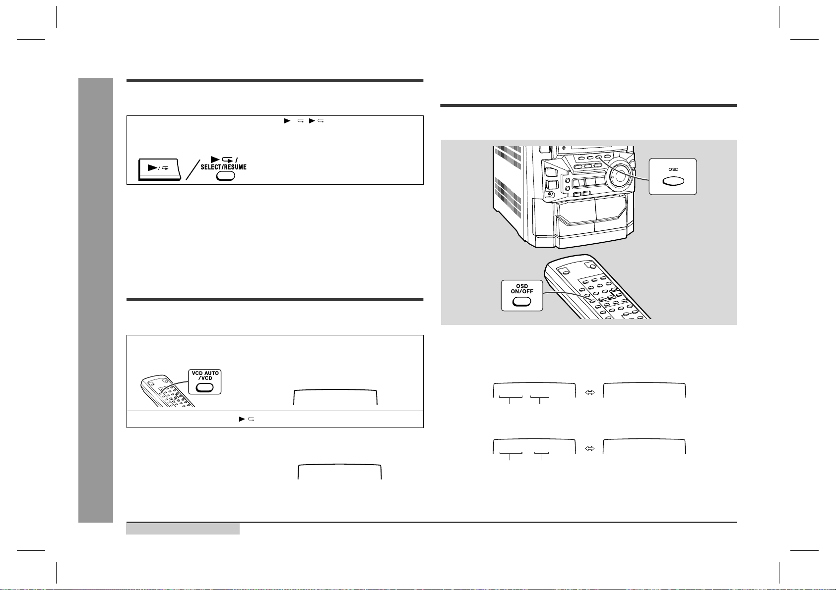
CD-BK110V/CD-BP99V
– 56 –
ICV1 RH-iX0495AWZZ : MPEG Controller (IX0495AW)
1* P50 VOCAL CANCEL Output Vocal cancel.
2* P51 K_C_DATA Output Key control IC data.
3* P52 K_C_CLOCK Output Key control IC clock.
4* P53 K_C_STROBE Output Key control IC strobe.
5* P54 KEY CONT. Output Key control.
6* P55 CD-SOL Output CD changer solenoid control.
7,8 P56, P57 NO USE Output Joint 10 kohm to GND.
9 VSS0 VSS0 — Ground voltage.
10 VDD0 VDD0 Input VDD
11* P30 CD-LD M+ Output CD changer motor control.
12* P31 CD-LD M- Output CD changer motor control.
13* P32 MO_SPEED Output CD changer motor speed control.
14 P33 NO USE Output Joint 10 kohm to GND.
15 P34 POWER_MPEG Output MPEG power supply control.
16,17 P35, P36 NO USE Output Joint 10 kohm to GND.
18 P20 MDI Input Comunicate to system microcomputer DI.
19 P21 MDO Output Comunicate to system microcomputer DO.
20 P22 MCK Input Comunicate to system microcomputer CLK.
21 P23 NO USE Output Joint 10 kohm to GND.
22 P24 MBUSY Output Comunicate to system microcomputer MBUSY.
23 P25/ASCK0 NO USE Output Joint 10 kohm to GND.
24 VDD1 VDD1 Input VDD
25 AVSS AVSS — Ground
26-33 P17-P10 NO USE Output Joint 10 kohm to GND.
34 AVREF AVREF Input Conect to VDD.
35 AVDD AVDD Input Conect to VDD.
36 RESET RESET Input Common use DSP_RESET.
37* XT2 XT2 — Open
38 XT1 XT1 Input Conect to VDD.
39 IC IC — Conect to ground.
40 X2 X2 Output Main clock.
41 X1 X1 Input Main clock.
42 VSS1 VSS1 — Ground voltage.
43 INTP0 INT Output Interrupt request.
44 INTP1 SBUSY Input Comunicate to system microcomputer SBUSY.
45,46 P02, P03 NO USE Output Joint 10 kohm to GND.
47-50 P70-P73 NO USE Output Joint 10 kohm to GND.
51 P74 MPEG RESET Output MPEG decoder reset.
52 BUZ HCS Output Chip select.
53 P64/RD HRD Output Read strobe.
54 WR HWR Output Write strobe.
55 WAIT HDAK Input Bus cycle acknowledge.
56 ASTB HA Output Address strobe.
57-64 AD0-AD7 HD0-HD7 Input/Output Host parallel interface.
Pin No. Port Name
Terminal Name
Input/Output
Function
In this unit, the terminal with asterisk mark (*) is open terminal which is not connected to the outside.
– 57 –
CD-BK110V/CD-BP99V
1 VDD Input Digital supply.
2-5 HD7-HD4 Input/Output Host data bus.
HD7 = MSB, HDO = LSB.
Internally pulled down. Pull down resistance = approx. 42 kohms.
Can quit this pull down with the HD_PD_OFF register (74H, bo).
6 GND — Ground
7-10 HD3-HD0 Input/Output Host data bus.
HD7 = MSB, HD0 = LSB.
Internally pulled down. Pull down resistance is approx. 42 kohms.
Can quit this pull down with the HD_PD_OFF register (74H, bo).
11,12 GND — Ground
13 X1 Input To connect a 27 MHz oscillator.
Open when not using.
14 X2 Input To connect a 27 MHz oscillator or input 27 MHz clock.
Set the clock at CKSEL terminal.
Signal input at 3.3 Vp-p.
15 VDD Input Digital supply.
16 CKSEL Input Select a clock to be input to X2 terminal.
Use CKSEL = High: oscillator.
CKSEL = Low : 27 MHz clock input.
17 VDD Input Digital supply.
18 GND — Ground
19 HCS Input Chip select signal.
20 HRD Input Read strobe signal.
21 HWR Input Write strobe signal.
22 HA Input Address/address strobe signal.
23 HSELA Input Host interface select signal.
Select a serial interface or an 8-bit parallel interface.
HSELX = High: parallel interface.
HSELX = Low: serial interface.
24 HSELA Input Host interface mode select signal.
Select multiplex mode or separate mode.
HSELA = High: multiplex mode.
HSELA = Low: separate mode.
Fixed low when using serial interface.
25 VDD Input Digital supply.
26 GND — Ground
27 RESET Input Reset terminal.
28 HDAK Output Host bus acknowledge signal.
29 INT Output Interrupt signal.
30 GND — Ground
31 AUCLK Input Audio clock (16.9344 MHz).
32 AUBCK Output Audio bit clock.
33 AULRCK Output Audio L/R clock.
34 AUEMPH Output Audio emphasis signal.
35 AUDO Output Audio data output.
36 VDD Input Digital supply.
37 GND — Ground
38-42 MA8-MA4 Output DRAM address bus.
MA8 = MSB, MAO = LSB.
43 GND — Ground
44 VDD Input Digital supply.
45-48 MA3-MA0 Output DRAM address bus.
MA8 = MSB, MA0 = LSB.
49 MRAS Output DRAM low address strobe signal.
50 GND — Ground
51 VDD Input Digital supply.
ICV2 VHiD61012GC-1 : MPEG Decoder (D61012GC) (1/2)
Pin No. FunctionTerminal Name Input/Output
CD-BK110V/CD-BP99V
– 58 –
52 MWE Output DRAM write enable signal.
53 MCAS Output DRAM column address strobe signal.
54-56 MD7-MD5 Input/Output DRAM data bus.
MD15 = MSB, MD0 = LSB.
Internally pulled down. Pull down resistance is approx. 42 kohms.
Can quit this pull down with the MD_PD_OFF register (74H, b1).
57 GND — Ground
58-62 MD4-MD0 Input/Output TDRAM data bus.
MD15 = MSB, MD0 = LSB.
Internally pulled down. Pull down resistance is approx. 42 kohms.
Can quit this pull down with the MD_PD_OFF register (74H, b1).
63 VDD Input Digital supply.
64 GND — Ground
65-68 MD15-MD12 Input/Output DRAM data bus.
MD15 = MSB, MD0 = LSB.
Internally pulled down. Pull down resistance is approx. 42 kohms.
Can quit this pull down with the MD_PD_OFF register (74H, b1).
69 GND — Ground
70-73 MD11-MD8 Input/Output DRAM data bus.
MD15 = MSB, MD0 = LSB.
Internally pulled down. Pull down resistance is approx. 42 kohms.
Can quit this pull down with the MD_PD_OFF register (74H, b1).
74 GND — Ground
75 VDD Input Digital supply.
76 GND — Ground
77* VCLK — Not used.
78* CSYNC Output Synchronized signal generating signal.
79* NSYNC Output Synchronized signal generating signal.
80* HSYNC Output Synchronized signal generating signal.
81*,82* — — Not used.
83 VDD Input Digital supply.
84 AVDD Input Analog power supply.
85 CBP1 Output 3CH Video D/A signal.
86 VOUT1 Output 3CH Video D/A signal.
87 CBP2 Output 3CH Video D/A signal.
88* VOUT2 Output 3CH Video D/A signal.
89 CBP3 Output 3CH Video D/A signal.
90* VOUT3 Output 3CH Video D/A signal.
91 AGND — Analog power supply.
92 VDD Input Digital supply.
93* — — Not used.
94 GND — Ground
95 CDC2PO Input CD data input.
96 CDEMPH Input CD data input.
97 CDLRCK Input CD data input.
98 CDBCK Input CD data input.
99 CDI Input CD data input.
100 GND — Ground
ICV2 VHiD61012GC-1 : MPEG Decoder (D61012GC) (2/2)
Pin No. FunctionTerminal Name Input/Output
In this unit, the terminal with asterisk mark (*) is open terminal which is not connected to the outside.
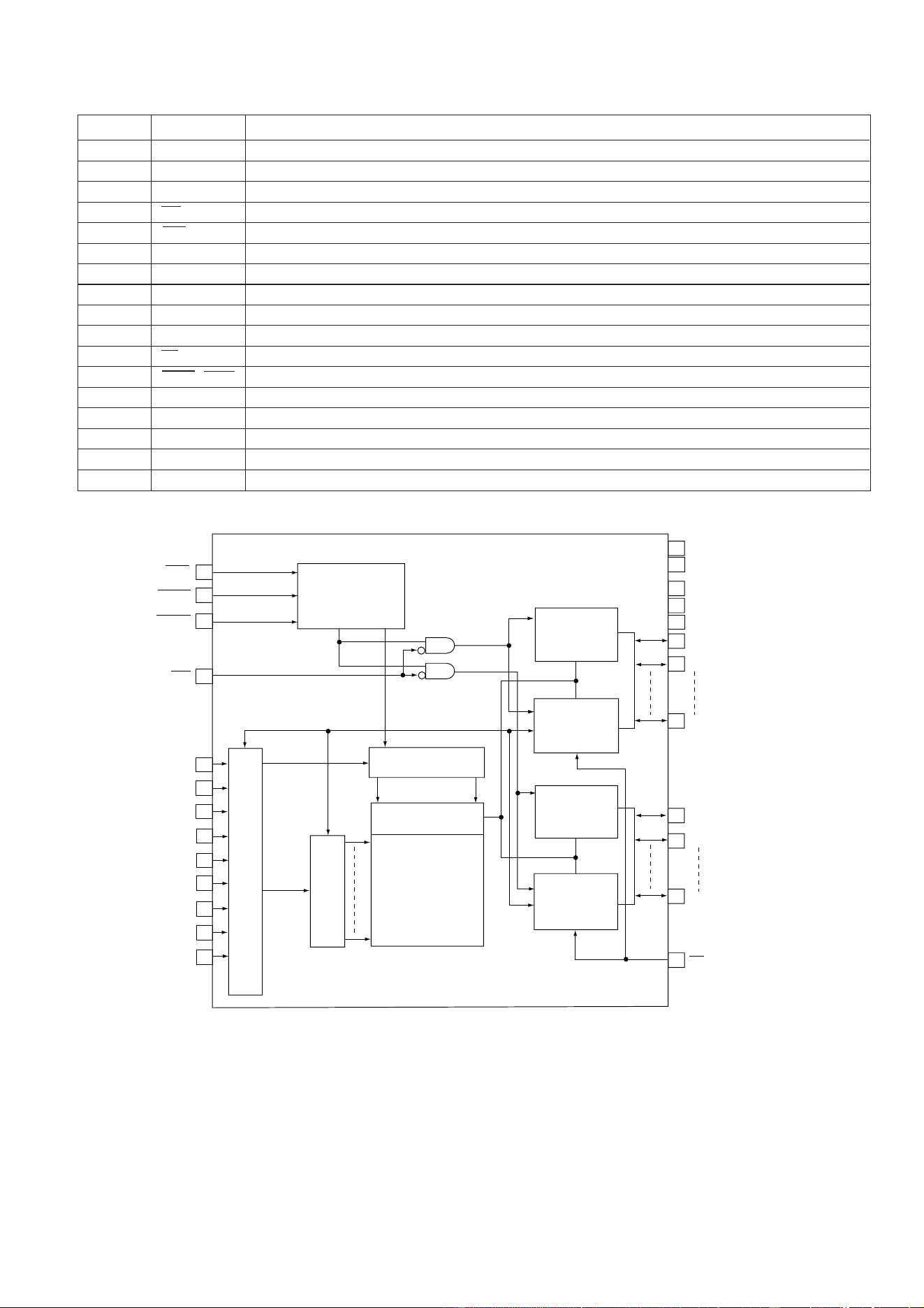
– 59 –
CD-BK110V/CD-BP99V
Pin No.
Port Name
Function
1 VCC Power supply.
2-10 I/O0-I/O7 Data input/output.
11*,12* N.C. Not used.
13 WE Read/write enable.
14 RAS Row address strobe.
15* NC Not used.
16-19 A0-A3 Address input. (row/refresh: A0 to A3) (Column: A0 to A3)
20 VCC Power supply.
21 VSS Ground
22-26 A4-A8 Address input. (row/refresh: A4 to A8) (Column: A4 to A8)
27 OE Output enable.
28,29 UCAS, LCAS Column address strobe.
30* N.C. Not used.
31-34 I/O8-I/O11 Data input/output.
35 VSS Ground
36-39 I/O12-I/O15 Data input/output.
40 VSS Ground
ICV3 VHiSDM4260C-1 : DRAM (SDM4260C)
In this unit, the terminal with asterisk mark (*) is open terminal which is not connected to the outside.
RAS
LCAS
UCAS
WE
A0
A1
A2
A3
A4
A5
A6
A7
A8
VCC
VSS
I/O0
I/O1
I/O7
I/O8
I/O9
I/O15
OE
Lowar
Upper
Clock generating
circuit
Lower data
Input buffer
Lower data
Output buffer
Coidmn decoder
Upper data
Input buffer
A0-A8
A0-A8
I/O control circuit
Memory cell array
Upper data
Output buffer
Roe decoder
Row and column address buffer
14
29
28
13
16
17
18
19
22
23
24
25
26
27
39
32
31
10
3
2
40
35
21
1
20
Figure 59 BLOCK DIAGRAM OF IC
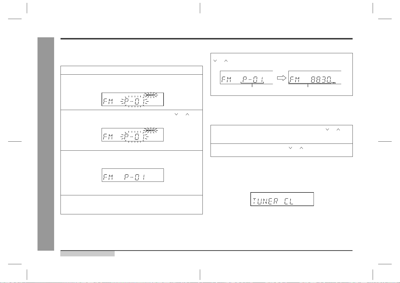
CD-BK110V/CD-BP99V
– 60 –
FL701 VVKSVA9MS13-1 : FL Display
FL DISPLAY
P1
P2
P3
P4
P5
P6
P7
P8
P9
P10
P11
P12
P13
P14
P15
P16
P17
P18
P19
P20
1G
U
T
V
W
a
b
k
j
h
f
m
d
g
p
e
n
r
c
s
2G
U
T
V
W
a
b
k
j
h
f
m
d
g
p
e
n
r
c
s
3G
U
T
V
W
a
b
k
j
h
f
m
d
g
p
e
n
r
c
s
4G
U
T
V
W
a
b
k
j
h
f
m
d
g
p
e
n
r
c
s
5G
U
T
V
W
a
b
k
j
h
f
m
d
g
p
e
n
r
c
s
6G
U
T
V
W
a
b
k
j
h
f
m
d
g
p
e
n
r
c
s
7G
U
T
V
W
a
b
k
j
h
f
m
d
g
p
e
n
r
c
s
8G
U
T
V
W
a
b
k
j
h
f
m
d
g
p
e
n
r
c
s
9G
2G 3G 4G 5G 6G 7G 8G 9G1G
a
b
c
d
f
g
m
e
r
p
n
h
j
k
V
T
U
W
s
:
(L)
(R)
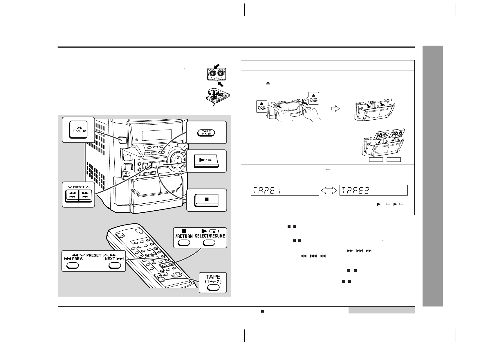
CD-BK110V/CD-BP99V
PARTS GUIDE
NOTE:
Parts marked with “ ” are important for maintaining the safety of the set.
Be sure to replace parts with specified ones for maintaining the safety and performance of the set.
“HOW TO ORDER REPLACEMENT PARTS”
To have your order filled promptly and correctly, please furnish the
following information.
1. MODEL NUMBER 2. REF. No.
3. PART NO. 4. DESCRIPTION
MARK: SPARE PARTS-DELIVERY SECTION
For U.S.A. only
Contact your nearest SHARP Parts Distributor to order.
For location of SHARP Parts Distributor,
Please call Toll-Free;
1-800-BE-SHARP
Explanation of capacitors/resistors parts codes
Capacitors
VCC ....................... Ceramic type
VCK........................ Ceramic type
VCT ........................ Semiconductor type
VC • • MF ............... Cylindrical type (without lead wire)
VC • • MN............... Cylindrical type (without lead wire)
VC • • TV................ Square type (without lead wire)
VC • • TQ ............... Square type (without lead wire)
VC • • CY ............... Square type (without lead wire)
VC • • CZ ............... Square type (without lead wire)
VC • • • • • • • • • J .. The 13th character represents capacity difference.
("J" ±5%, "K" ±10%, "M" ±20%, "N" ±30%,
"C" ±0.25 pF, "D" ±0.5 pF, "Z" +80-20%.)
If there are no indications for the electrolytic capacitors, error is ±20%.
Resistors
VRD ....................... Carbon-film type
VRS........................ Carbon-film type
VRN ....................... Metal-film type
VR • • MF ............... Cylindrical type (without lead wire)
VR • • MN............... Cylindrical type (without lead wire)
VR • • TV................ Square type (without lead wire)
VR • • TQ ............... Square type (without lead wire)
VR • • CY ............... Square type (without lead wire)
VR • • CZ ............... Square type (without lead wire)
VR • • • • • • • • • J .. The 13th character represents error.
("J" ±5%, "F" ±1%, "D" ±0.5%.)
If there are no indications for other parts, the resistors are ±5%
carbon-film type.
VIDEO CD MINI SYSTEM
MODEL CD-BK110V
CD-BK110V Video CD Mini System consisting of
CD-BK110V (main unit) and CP-BK110 (speaker system).
VIDEO CD MINI SYSTEM
MODEL CD-BP99V
CD-BP99V Video CD Mini System consisting of
CD-BP99V (main unit) and CP-BP99 (speaker system).

PRICE
RANK
DESCRIPTION
NO.
PART CODE
NO. PARTS CODE
PRICE
RANK
DESCRIPTION
CD-BK110V/CD-BP99V
– 1 –
INTEGRATED CIRCUITS
IC1 VHILA9235M/-1 J AQ Servo Amp.,LA9235M
IC2 VHILC78636E-1 J AX Servo/Signal Control,LC78636E
IC3 VHIM63001FP-1 J AX Focus/Tracking/Spin/Sled Driver,
M63001FP
IC101 VHIAN7345K/-1 J AM Record/Playback Amp.,AN7345K
IC301 VHITA7358AP-1 J AG FM Front End,TA7358AP
IC302 VHILC72131/-1 J AP PLL (Tuner),LC72131
IC303 VHILA1832S/-1 J AN FM IF Det./FM Mpx./AM IF,
LA1832S
IC601 VHILC75341/-1 J AM Audio Processor,LC75341
IC701 RH-IX0338AWZZ J AW System Microcomputer,
IX0338AW
IC704 VHIKIA7042AP1 J AC System Reset,KIA7042A
IC901 VHILA4282//-1 J AM
Power Amp.,LA4282 [CD-BK110V]
IC901 92L28405415000 J
Power Amp.,BA5415A [CD-BP99V]
IC902 VHIKIA7810AP1 J AF Voltage Regulator,KIA7810AP
IC904 VHIKIA7805AP1 J AF Voltage Regulator,KIA7805AP
ICV1 RH-IX0495AWZZ J AX MPEG Controller,IX0495AW
ICV2 VHID61012GC-1 J BP MPEG Decoder,D61012GC
ICV3 VHISDM4260C-1 J AY DRAM,SDM4260C
ICV4 VHINJM2267M-1 J AH
Video Operation Amp.,NJM2267M
TRANSISTORS
Q1 VSKTC3265Y/-1 J AC Silicon,NPN,KTC3265 Y
Q2 VSKRC102M//-1 J AC Digital,NPN,KRC102 M
Q3,4 VSKTA1504GR-1 J AB Silicon,PNP,KTA1504 GR
Q101 VSKTA1266GR-1 J AB Silicon,PNP,KTA1266 GR
Q102,103 VSKRC104M//-1 J AC Digital,NPN,KRC104 M
Q104~107 VS2SC1845F/-1 J AC Silicon,NPN,2SC1845 F
Q108~111 VS2SC3331//-1 J AB Silicon,NPN,2SC3331 S
Q112 VSKTA1266GR-1 J AB Silicon,PNP,KTA1266 GR
Q113 VSKRC104M//-1 J AC Digital,NPN,KRC104 M
Q114 VSKTC3203Y/-1 J AC Silicon,NPN,KTC3203 Y
Q302 VSKTC3194Y/-1 J AD Silicon,NPN,KTC3194 Y
Q360 VSKTA1266GR-1 J AB Silicon,PNP,KTA1266 GR
Q401~408 92L2830901403 J Silicon,NPN,9014 C
[CD-BK110V Only]
Q601,602 VS2SC3331//-1 J AB Silicon,NPN,2SC3331 S
Q701 VSKRC107M//-1 J AC Digital,NPN,KRC107 M
Q704,705 VSKTA1271Y/-1 J AC Silicon,PNP,KTA1271 Y
Q706 VSKTA1273Y/-1 J AE Silicon,PNP,KTA1273 Y
Q707 VSKRC102M//-1 J AC Digital,NPN,KRC102 M
Q708 VSKRC107M//-1 J AC Digital,NPN,KRC107 M
Q901,902 VSKRC102M//-1 J AC Digital,NPN,KRC102 M
[CD-BK110V Only]
Q904 VSKTA1266GR-1 J AB Silicon,PNP,KTA1266 GR
Q905 VSKTC2026//-1 J AF Silicon,NPN,KTC2026
QV2 VSKTA1298Y/-1 J AC Silicon,PNP,KTA1298 Y
QV3 VSKRC102M//-1 J AC Digital,NPN,KRC102 M
QV4 VSKTA1298Y/-1 J AC Silicon,PNP,KTA1298 Y
DIODES
D21,22 VHD1SS133//-1 J AA Silicon,1SS133
D301~306 VHD1SS133//-1 J AA Silicon,1SS133
D303A VHD1SS133//-1 J AA Silicon,1SS133
D304A VHD1SS133//-1 J AA Silicon,1SS133
D701~703 VHD1SS133//-1 J AA Silicon,1SS133
D707~711 VHD1SS133//-1 J AA Silicon,1SS133
D714 VHD1SS133//-1 J AA Silicon,1SS133
D716 VHD1SS133//-1 J AA Silicon,1SS133
D901 92L2810414800 J
Silicon,1N4148 [CD-BP99V Only]
D902 92L2810400130 J Silicon,1N4001
D907~917 VHD1N4004S/-1 J AB Silicon,1N4004S
D918~920 VHD1SS133//-1 J AA Silicon,1SS133
D922 VHEDZ3R9BSB-1 J AC Zener,3.9V,DZ3.9BSB
DV4,5 VHD1SS133//-1 J AA Silicon,1SS133
LED722 VHP4204SRT7-1 J AD LED,Red,4204SRT7
ZD61 VHEDZ3R9BSB-1 J AC Zener,3.9V,DZ3.9BSB
ZD902 VHEDZ300BSB-1 J AB Zener,30V,DZ30BSB
ZD903 VHEMTZJ6R2A-1 J AA Zener,6.2V,MTZJ6.2A
FILTERS
BF301 RFILR0008AWZZ J AE Band Pass Filter
CF302 RFILF0124AFZZ J AD FM IF,10.7 MHz
CF351 RFILF0003AWZZ J AK FM IF,10.7 MHz
CF352 RFILA0009AWZZ J AE AM IF,450 kHz
TRANSFORMERS
1 PT801 92L2950090W710 J Power with CNS801/CNS901
[CD-BP99V]
1 PT801 92L2950100W710 J BC Power with CNS801/CNS901
[CD-BK110V]
T301 RCILB0065AWZZ J AC FM OSC.
T302 RCILI0017AWZZ J AB FM IF
T303 RCILA0052AWZZ J AE AM Antenna
T306 RCILB0058AWZZ J AC AM OSC.
T351 RCILI0019AWZZ J AD AM IF
COILS
L61 VP-XHR82K0000 J AC 0.82 µH,Choke
L62 VP-XH2R2K0000 J AB 2.2 µH,Choke
L63,64 VP-XHR82K0000 J AC 0.82 µH,Choke
L103 VP-DH101K0000 J AB 100 µH,Choke
L104 VP-MK331K0000 J AB 330 µH,Choke
L312 RCILR0056AWZZ J AB FM RF
L351,352 VP-DH101K0000 J AB 100 µH,Choke
L701 VP-DH101K0000 J AB 100 µH,Choke
VARIABLE RESISTOR
VR401 92L29200503030 J AG 50 kohms (A) [Mic Volume]
[CD-BK110V Only]
VARIABLE CAPACITORS
VD301 VHCSVC348S/-1 J AK Variable Capacitance,SVC348S
VD302,303 VHCSVC211C/-1 J AG Variable Capacitance,SVC211C
VIBRATORS
X351 92LCRSTL1425A J AF Crystal,456 kHz
X352 RCRSP0002AWZZ J AH Crystal,4.5 MHz
XL1 92LCRSTL1746A J AC Crystal,16.943 MHz
XL701 RCRSP0003AWZZ J AH Crystal,4.1943 MHz
XV1 RCRM-0201AFZZ J AD Ceramic,4.19 MHz
XV2 RCRSP0013AWZZ J AG Crystal,27 MHz
CAPACITORS
C6 92L2756010702 J 100 µF,10V,Electrolytic
C7 92L2756010604 J 10 µF,16V,Electrolytic
C8 92L27100223108 J 0.022 µF,50V
C11 92L2756047602 J 47 µF,10V,Electrolytic
C12 92L27100223108 J 0.022 µF,50V
C13 92L27100103108 J 0.01 µF,50V
C14 92L27100334008 J 0.33 µF,50V
C17 92L27100472108 J 0.0047 µF,50V
C18 92L27100060108 J 6 pF,50V
C20,21 92L27100104108 J 0.1 µF,25V
C22 92L27100101108 J 100 pF,50V
C23 92L27100473108 J 0.047 µF,50V
C24 92L2756022507 J 2.2 µF,50V,Electrolytic
C25 92L27100223108 J 0.022 µF,50V
C26 92L27100473108 J 0.047 µF,50V
C27 92L27100104108 J 0.1 µF,25V
C28 92L2756047602 J 47 µF,10V,Electrolytic
C29,30 92L27100223108 J 0.022 µF,50V
C31 92L2756010702 J 100 µF,10V,Electrolytic
C34 92L27100223108 J 0.022 µF,50V
C38,39 92L2756010604 J 10 µF,16V,Electrolytic
C40 92L27100152108 J 0.0015 µF,50V
C41 92L2756010702 J 100 µF,10V,Electrolytic
C42 92L27100680508 J 68 pF,50V
C43 92L27100152108 J 0.0015 µF,50V
C44 92L27100223108 J 0.022 µF,50V
C45 92L2756010702 J 100 µF,10V,Electrolytic
C46 92L27100223108 J 0.022 µF,50V
CD-BK110V/CD-BP99V
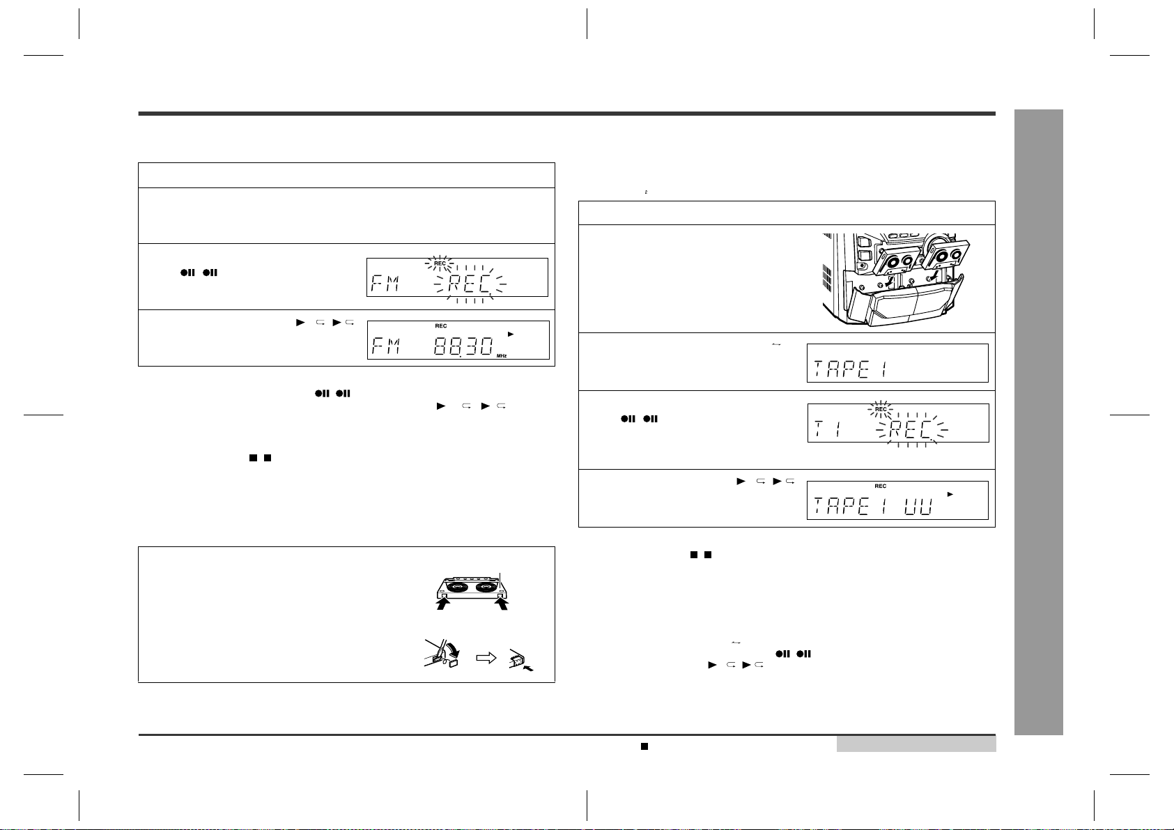
NO.
PRICE
RANK
DESCRIPTIONPARTS CODE
NO. PART CODE
PRICE
RANK
DESCRIPTION
CD-BK110V/CD-BP99V
– 2 –
C47 92L2756010702 J 100 µF,10V,Electrolytic
C49,50 92L2756010702 J 100 µF,10V,Electrolytic
C51 92L2756047602 J 47 µF,10V,Electrolytic
C52 92L27100103108 J 0.01 µF,50V
C53 92L27100102108 J 0.001 µF,50V
C54 92L2756047602 J 47 µF,10V,Electrolytic
C55 92L27100103108 J 0.01 µF,50V
C56 92L27520477001 J 470 µF,6.3V,Electrolytic
C57,58 92L27100270108 J 27 pF,50V
C64 92L2756047602 J 47 µF,10V,Electrolytic
C71~78 92L27100101108 J 100 pF,50V
C80 92L27100104108 J 0.1 µF,25V
C81~83 92L27100223108 J 0.022 µF,50V
C101 VCKZPA1HF473Z J AA 0.047 µF,50V
C102,103 92L2700056143 J 560 pF,50V
C104,105 92L2700018143 J 180 pF,50V
C106,107 92L2700056143 J 560 pF,50V
C108 VCEAZA1CW107M J AC 100 µF,16V,Electrolytic
C109 92L2700010243 J 0.001 µF,50V
C110 VCEAZA1HW106M J AB 10 µF,50V,Electrolytic
C112~115 92L2700033143 J 330 pF,50V
C116,117 VCEAZA1CW107M J AC 100 µF,16V,Electrolytic
C118,119 92L2760033322 J 0.033 µF,100V,Mylar
C120,121 92L2700056143 J 560 pF,50V
C122,123 VCEAZA1HW105M J AB 1 µF,50V,Electrolytic
C126,127 92L2700027143 J 270 pF,50V
C128,129 VCEAZA1HW226M J AB 22 µF,50V,Electrolytic
C130,131 VCKZPA1HF223Z J AA 0.022 µF,50V
C132,133 92L2700033243 J 0.0033 µF,50V
C134,135 VCEAZA1HW476M J AB 47 µF,50V,Electrolytic
C136 VCEAZA1HW226M J AB 22 µF,50V,Electrolytic
C137 VCKZPA1HF223Z J AA 0.022 µF,50V
C138 VCEAZA0JW227M J AC 220 µF,6.3V,Electrolytic
C139 VCEAZA1HW335M J AB 3.3 µF,50V,Electrolytic
C140 VCQPKA2AA822J J AA 0.0082 µF,100V,Polypropylene
C141 VCQYKA1HM393K J AB 0.039 µF,50V,Mylar
C142 VCEAZA1HW476M J AB 47 µF,50V,Electrolytic
C145~147 92L2700010243 J 0.001 µF,50V
C148 VCKZPA1HF473Z J AA 0.047 µF,50V
C150 92L2700033243 J 0.0033 µF,50V
C301,302 92L2700010243 J 0.001 µF,50V
C303 92L2691010043 J 10 pF,50V
C304 92L2700010243 J 0.001 µF,50V
C304A 92L2691010143 J 100 pF,50V
C305 92L2691005043 J 5 pF,50V
C306 VCKZPA1HF223Z J AA 0.022 µF,50V
C307 VCEAZA1HW106M J AB 10 µF,50V,Electrolytic
C308 92L2691005043 J 5 pF,50V
C309 92L2700010243 J 0.001 µF,50V
C310 92L2691015043 J 15 pF,50V
C311 92L2691018043 J 18 pF,50V
C312 VCKZPA1HF223Z J AA 0.022 µF,50V
C313 92L2691022043 J 22 pF,50V
C314,315 92L2700047243 J 0.0047 µF,50V
C316,317 92L2700010243 J 0.001 µF,50V
C318,319 92L2691010143 J 100 pF,50V
C320 VCKZPA1HF223Z J AA 0.022 µF,50V
C321,322 92L2700010243 J 0.001 µF,50V
C323 VCKZPA1HF223Z J AA 0.022 µF,50V
C324 92L2691004043 J 4 pF,50V
C330 92L2691015043 J 15 pF,50V
C331 VCKZPA1HF473Z J AA 0.047 µF,50V
C332 VCKZPA1HF223Z J AA 0.022 µF,50V
C334 92L2691027043 J 27 pF,50V
C335 92L2700056143 J 560 pF,50V
C342 VCKZPA1HF223Z J AA 0.022 µF,50V
C350,351 VCKZPA1HF223Z J AA 0.022 µF,50V
C352 VCEAZA1HW106M J AB 10 µF,50V,Electrolytic
C353,354 VCKZPA1HF223Z J AA 0.022 µF,50V
C355 92L2691022043 J 22 pF,50V
C356 92L2700010243 J 0.001 µF,50V
C357 VCEAZA1HW225M J AB 2.2 µF,50V,Electrolytic
C358 VCEAZA1HW105M J AB 1 µF,50V,Electrolytic
C361 VCKZPA1HF223Z J AA 0.022 µF,50V
C362 VCEAZA1HW335M J AB 3.3 µF,50V,Electrolytic
C363 VCKZPA1HF223Z J AA 0.022 µF,50V
C364 VCEAZA1HW106M J AB 10 µF,50V,Electrolytic
C365 VCKZPA1HF223Z J AA 0.022 µF,50V
C366 92L2700010243 J 0.001 µF,50V
C367,368 VCEAZA1HW105M J AB 1 µF,50V,Electrolytic
C369 92L2691027043 J 27 pF,50V
C370~372 VCEAZA1HW105M J AB 1 µF,50V,Electrolytic
C373,374 92L2760015322 J 0.015 µF,100V,Mylar
C380 VCEAZA1HW106M J AB 10 µF,50V,Electrolytic
C381 92L2691012043 J 12 pF,50V
C382 92L2691015043 J 15 pF,50V
C385 92L2700010343 J 0.01 µF,50V
C386 92L2700033143 J 330 pF,50V
C387 VCKZPA1HF223Z J AA 0.022 µF,50V
C391 VCEAZA1CW476M J AB 47 µF,16V,Electrolytic
C392 92L2700010243 J 0.001 µF,50V
C393 VCEAZA1HW105M J AB 1 µF,50V,Electrolytic
C394 VCEAZA1CW476M J AB 47 µF,16V,Electrolytic
C395 VCKZPA1HF223Z J AA 0.022 µF,50V
C396 VCEAZA1CW107M J AC 100 µF,16V,Electrolytic
C397 VCKZPA1HF223Z J AA 0.022 µF,50V
C398 VCEAZA1CW107M J AC 100 µF,16V,Electrolytic
C399 VCKZPA1HF223Z J AA 0.022 µF,50V
C401,402 VCEAZA1HW105M J AB 1 µF,50V,Electrolytic
[CD-BK110V Only]
C403 VCKYPA1HB221K J AA 220 pF,50V [CD-BK110V Only]
C404 VCEAZA1HW105M J AB 1 µF,50V,Electrolytic
[CD-BK110V Only]
C405 92L2700047243 J
0.0047 µF,50V [CD-BK110V Only]
C406 VCEAZA1HW105M J AB 1 µF,50V,Electrolytic
[CD-BK110V Only]
C407 VCEAZA1HW475M J AB 4.7 µF,50V,Electrolytic
[CD-BK110V Only]
C408 VCEAZA0JW227M J AC 220 µF,6.3V,Electrolytic
[CD-BK110V Only]
C409 VCEAZA1HW105M J AB 1 µF,50V,Electrolytic
[CD-BK110V Only]
C411 VCEAZA0JW227M J AC 220 µF,6.3V,Electrolytic
[CD-BK110V Only]
C412,413 VCEAZA1HW105M J AB 1 µF,50V,Electrolytic
[CD-BK110V Only]
C414 VCEAZA0JW227M J AC 220 µF,6.3V,Electrolytic
[CD-BK110V Only]
C420,421 VCEAZA1HW105M J AB 1 µF,50V,Electrolytic
[CD-BK110V Only]
C433 VCEAZA1HW105M J AB 1 µF,50V,Electrolytic
[CD-BK110V Only]
C440,441 VCEAZA1HW105M J AB 1 µF,50V,Electrolytic
[CD-BK110V Only]
C601,602 92L2700010243 J 0.001 µF,50V
C603 VCEAZA1HW105M J AB 1 µF,50V,Electrolytic
C604 VCEAZA1EW107M J AB 100 µF,25V,Electrolytic
C605 VCKZPA1HF223Z J AA 0.022 µF,50V
C606 VCEAZA1HW226M J AB 22 µF,50V,Electrolytic
C607,608 VCEAZA1HW106M J AB 10 µF,50V,Electrolytic
C609~612 VCQYKA1HM104K J AB 0.1 µF,50V,Mylar
C613,614 92L2760027222 J 0.0027 µF,100V,Mylar
C615,616 VCKYPA1HB221K J AA 220 pF,50V
C617,618 VCEAZA1HW105M J AB 1 µF,50V,Electrolytic
C619 VCKYPA1HB221K J AA 220 pF,50V
C623~630 VCEAZA1HW105M J AB 1 µF,50V,Electrolytic
C701 VCKZPA1HF223Z J AA 0.022 µF,50V
C702 92L2750010801 J 1000 µF,6.3V,Electrolytic
C703,704 92L2691030043 J 30 pF,50V
C705 VCEAZA1AW107M J AB 100 µF,10V,Electrolytic
C707,708 VCEAZA1HW105M J AB 1 µF,50V,Electrolytic
C710 VCEAZA1CW476M J AB 47 µF,16V,Electrolytic
C713 RC-EZD104AF1H J AB 0.1 µF,50V,Electrolytic
C714 92L2700010363 J 0.01 µF,50V
C715 VCEAZA1HW335M J AB 3.3 µF,50V,Electrolytic
C716 VCKZPA1HF223Z J AA 0.022 µF,50V
C717 VCEAZA1CW106M J AC 10 µF,16V,Electrolytic
C718 VCKZPA1HF223Z J AA 0.022 µF,50V
C719 VCEAZA1CW476M J AB 47 µF,16V,Electrolytic
C720 VCEAZA1HW105M J AB 1 µF,50V,Electrolytic
C901 VCQYKA1HM104K J AB 0.1 µF,50V,Mylar
[CD-BP99V Only]
C902 VCEAZA1CW476M J AB 47 µF,16V,Electrolytic
[CD-BP99V Only]
C903,904 92L2700047143 J 470 pF,50V
C905 VCKZPA1HF223Z J AA 0.022 µF,50V [CD-BK110V]
C905 92L2750010805 J 1000 µF,25V,Electrolytic
[CD-BP99V]
C906 VCEAZA1CW107M J AC 100 µF,16V,Electrolytic
[CD-BK110V]
C906 VCQYKA1HM104K J AB 0.1 µF,50V,Mylar [CD-BP99V]
C907 VCEAZA1CW476M J AB 47 µF,16V,Electrolytic
[CD-BP99V]
C907 VCEAZA1EW107M J AB 100 µF,25V,Electrolytic
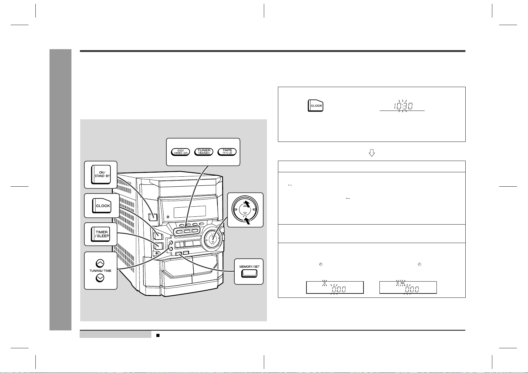
PRICE
RANK
DESCRIPTION
NO.
PART CODE
NO. PARTS CODE
PRICE
RANK
DESCRIPTION
CD-BK110V/CD-BP99V
– 3 –
[CD-BK110V]
C908 VCQYKA1HM823K J AC
0.082 µF,50V,Mylar [CD-BK110V]
C908 92L2750010805 J 1000 µF,25V,Electrolytic
[CD-BP99V]
C909 VCQYKA1HM823K J AC 0.082 µF,50V,Mylar
[CD-BK110V Only]
C910 VCEAZA1EW107M J AB 100 µF,25V,Electrolytic
[CD-BK110V Only]
C911 VCEAZA1CW107M J AC 100 µF,16V,Electrolytic
[CD-BP99V]
C911 VCKZPA1HF223Z J AA 0.022 µF,50V [CD-BK110V]
C912 VCEAZA1CW107M J AC 100 µF,16V,Electrolytic
[CD-BP99V]
C912 VCQYKA1HM104K J AB 0.1 µF,50V,Mylar [CD-BK110V]
C913 VCQYKA1HM104K J AB 0.1 µF,50V,Mylar
[CD-BK110V Only]
C914 VCEAZA1CW107M J AC 100 µF,16V,Electrolytic
[CD-BP99V]
C914 VCEAZA1EW108M J AE 1000 µF,25V,Electrolytic
[CD-BK110V]
C915 VCEAZA1EW108M J AE 1000 µF,25V,Electrolytic
[CD-BK110V Only]
C916 VCEAZA1HW475M J AB 4.7 µF,50V,Electrolytic
[CD-BP99V]
C916 VCQYKA1HM104K J AB 0.1 µF,50V,Mylar [CD-BK110V]
C917 VCQYKA1HM104K J AB 0.1 µF,50V,Mylar
[CD-BK110V Only]
C918 VCKYPA1HB221K J AA 220 pF,50V [CD-BK110V Only]
C919 VCEAZA1HW106M J AB 10 µF,50V,Electrolytic
C933 VCCSPA1HL680J J AA 68 pF,50V
C934 VCQYKA1HM473K J AB 0.047 µF,50V,Mylar
C935 VCEAZA1HW226M J AB 22 µF,50V,Electrolytic
C938 VCEAZA1HW476M J AB 47 µF,50V,Electrolytic
C939,940 VCQYKA1HM104K J AB 0.1 µF,50V,Mylar
C943 VCEAZA1HW476M J AB 47 µF,50V,Electrolytic
C944 VCKZPA1HF223Z J AA 0.022 µF,50V
C945 VCQYKA1HM104K J AB 0.1 µF,50V,Mylar
C946 VCEAZW1HW228M J AH 2200 µF,50V,Electrolytic
[CD-BK110V]
C946 VCEAZW1VW338M J 3300 µF,35V,Electrolytic
[CD-BP99V]
C947 VCEAZW1VW338M J 3300 µF,35V,Electrolytic
C950~953 VCQYKA1HM473K J AB 0.047 µF,50V,Mylar
C954 VCEAZA1HW107M J AC 100 µF,50V,Electrolytic
C955~957 VCEAZA1HW476M J AB 47 µF,50V,Electrolytic
C958,959 VCEAZA1HW107M J AC 100 µF,50V,Electrolytic
CV1 92L2756047602 J 47 µF,10V,Electrolytic
CV2 92L27100223108 J 0.022 µF,50V
CV4 92L2756047602 J 47 µF,10V,Electrolytic
CV5 92L27100223108 J 0.022 µF,50V
CV6,7 92L27100270108 J 27 pF,50V
CV9 92L27100223108 J 0.022 µF,50V
CV10 92L2756047602 J 47 µF,10V,Electrolytic
CV11,12 92L27100223108 J 0.022 µF,50V
CV13,14 92L27100104108 J 0.1 µF,25V
CV15 92L27560475070 J 4.7 µF,50V,Electrolytic
CV16 92L27100104108 J 0.1 µF,25V
CV17 92L27100103108 J 0.01 µF,50V
CV18 92L2750010801 J 1000 µF,6.3V,Electrolytic
CV19~21 92L27100223108 J 0.022 µF,50V
CV22,23 92L2756047602 J 47 µF,10V,Electrolytic
CV24,25 92L27100223108 J 0.022 µF,50V
CV39 92L2750010801 J 1000 µF,6.3V,Electrolytic
CV40 92L2756022602 J 22 µF,10V,Electrolytic
CV41 92L27560475070 J 4.7 µF,50V,Electrolytic
CV44,45 92L27100270108 J 27 pF,50V
RESISTORS
R1 92L32150102008 J 1 kohm,1/10W
R2 92L32150152008 J 1.5 kohms,1/8W
R3 92L32150473008 J 47 kohms,1/8W
R4 92L32150103008 J 10 kohm,1/8W
R5 92L32150393008 J 39 kohms,1/8W
R6 92L32150273008 J 27 kohms,1/8W
R7 92L32150682008 J 6.8 kohms,1/8W
R8 92L32150331008 J 330 ohms,1/8W
R10 92L32150273008 J 27 kohms,1/8W
R11 92L32150123008 J 12 kohms,1/8W
R12,13 92L32150681008 J 680 ohms,1/8W
R14 92L32150122008 J 1.2 kohms,1/8W
R15,16 92L32150103008 J 10 kohm,1/8W
R17 92L32150102008 J 1 kohm,1/8W
R19 92L32150470008 J 47 ohms,1/8W
R20 92L32150221008 J 220 ohms,1/8W
R21,22 92L32150471008 J 470 ohms,1/8W
R25 92L32150103008 J 10 kohm,1/8W
R35 92L32150102008 J 1 kohm,1/8W
R38 92L32150271008 J 270 ohms,1/8W
R39 92L32150471008 J 470 ohms,1/8W
R40 92L32150122008 J 1.2 kohms,1/8W
R42 92L32150563008 J 56 kohms,1/8W
R44 92L32150102008 J 1 kohm,1/8W
R45 92L32150122008 J 1.2 kohms,1/8W
R46 92L32150102008 J 1 kohm,1/8W
R47 92L32159330008 J 3.3 ohms,1/8W
R48 92L32150682008 J 6.8 kohms,1/8W
R50 92L32150470008 J 47 ohms,1/8W
R51 92L32150683008 J 68 kohms,1/8W
R52,53 92L32150563008 J 56 kohms,1/8W
R54 92L32150683008 J 68 kohms,1/8W
R55,56 92L32150563008 J 56 kohms,1/8W
R58 92L32150221008 J 220 ohms,1/8W
R67,68 92L32150102008 J 1 kohm,1/8W
R71~78 92L32150102008 J 1 kohm,1/8W
R79 92L32150155008 J 1.5 Mohms,1/8W
R80 92L32150105008 J 1 Mohm,1/8W
R81,82 92L32150392008 J 3.9 kohms,1/8W
R83,84 92L32150103008 J 10 kohm,1/8W
R85 92L32150101008 J 100 ohm,1/8W
R86 92L32150102008 J 1 kohm,1/8W
R89~93 92L32150102008 J 1 kohm,1/8W
R94 92L32150332008 J 3.3 kohms,1/8W
R95 92L32150472008 J 4.7 kohms,1/8W
R96 92L32150102008 J 1 kohm,1/8W
R97 92L32150392008 J 3.9 kohms,1/8W
R101,102 VRD-ST2CD103J J AA 10 kohm,1/6W
R103 VRD-ST2CD472J J AA 4.7 kohms,1/6W
R104,105 VRD-ST2CD102J J AA 1 kohm,1/6W
R106,107 VRD-ST2CD222J J AA 2.2 kohms,1/6W
R108,109 VRD-ST2CD332J J AA 3.3 kohms,1/6W
R110 VRD-ST2CD473J J AA 47 kohms,1/6W
R111,112 VRD-ST2CD472J J AA 4.7 kohms,1/6W
R113 VRD-ST2CD473J J AA 47 kohms,1/6W
R114,115 VRD-ST2CD102J J AA 1 kohm,1/6W
R116,117 VRD-ST2CD560J J AA 56 ohms,1/6W
R118,119 VRD-ST2CD104J J AA 100 kohm,1/6W
R120,121 VRD-ST2CD392J J AA 3.9 kohms,1/6W
R122,123 VRD-ST2CD562J J AA 5.6 kohms,1/6W
R124,125 VRD-ST2CD123J J AA 12 kohms,1/6W
R126 VRD-ST2CD683J J AA 68 kohms,1/6W
R127,128 VRD-ST2CD682J J AA 6.8 kohms,1/6W
R129,130 VRD-ST2CD392J J AA 3.9 kohms,1/6W
R131,132 VRD-ST2CD122J J AA 1.2 kohms,1/6W [CD-BK110V]
R131,132 VRD-ST2CD152J J AA 1.5 kohms,1/6W [CD-BP99V]
R133,134 VRD-ST2CD101J J AA 100 ohm,1/6W
R135,136 VRD-ST2CD103J J AA 10 kohm,1/6W
R137,138 VRD-ST2CD153J J AA 15 kohms,1/6W
R139 VRD-ST2CD181J J AA 180 ohms,1/6W
R140,141 VRD-ST2CD103J J AA 10 kohm,1/6W
R142,143 VRD-ST2CD224J J AA 220 kohms,1/6W
R144 VRD-ST2CD473J J AA 47 kohms,1/6W
R145 VRD-ST2CD472J J AA 4.7 kohms,1/6W
R146 VRD-ST2EE820J J AA 82 ohms,1/4W
R147 VRD-ST2CD473J J AA 47 kohms,1/6W
R148 VRD-ST2CD223J J AA 22 kohms,1/6W
R149 VRD-ST2CD4R7J J AA 4.7 ohms,1/6W
R157 VRD-ST2CD101J J AA 100 ohm,1/6W
R302 VRD-ST2CD220J J AA 22 ohms,1/6W
R309 VRD-ST2CD103J J AA 10 kohm,1/6W
R311 VRD-ST2CD104J J AA 100 kohm,1/6W
R313 VRD-ST2CD333J J AA 33 kohms,1/6W
R314 VRD-ST2CD220J J AA 22 ohms,1/6W
R316 VRD-ST2CD472J J AA 4.7 kohms,1/6W
R322 VRD-ST2CD681J J AA 680 ohms,1/6W
R323 VRD-ST2CD683J J AA 68 kohms,1/6W
R325 VRD-ST2CD473J J AA 47 kohms,1/6W
R327 VRD-ST2CD330J J AA 33 ohms,1/6W
R336 VRD-ST2CD103J J AA 10 kohm,1/6W
R350 VRD-ST2CD272J J AA 2.7 kohms,1/6W
R351 VRD-ST2CD562J J AA 5.6 kohms,1/6W
R352 VRD-ST2CD102J J AA 1 kohm,1/6W
R353 VRD-ST2CD391J J AA 390 ohms,1/6W
R355 VRD-ST2CD332J J AA 3.3 kohms,1/6W
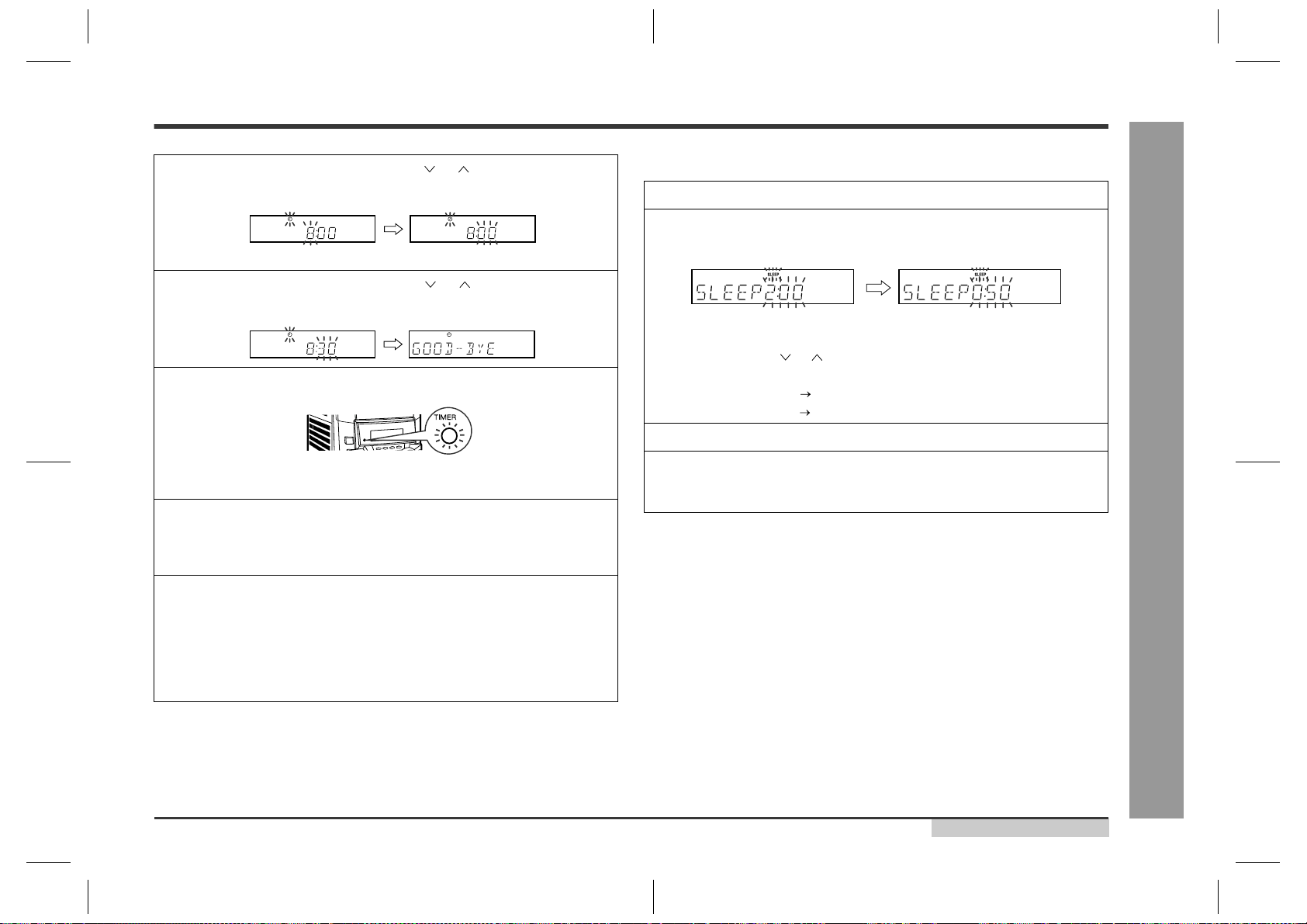
NO.
PRICE
RANK
DESCRIPTIONPARTS CODE
NO. PART CODE
PRICE
RANK
DESCRIPTION
CD-BK110V/CD-BP99V
– 4 –
R356 VRD-ST2CD102J J AA 1 kohm,1/6W
R357 VRD-ST2CD474J J AA 470 kohms,1/6W
R358 VRD-ST2CD392J J AA 3.9 kohms,1/6W
R359 VRD-ST2CD182J J AA 1.8 kohms,1/6W
R360 VRD-ST2CD472J J AA 4.7 kohms,1/6W
R361,362 VRD-ST2CD332J J AA 3.3 kohms,1/6W [CD-BP99V]
R361,362 VRD-ST2CD512J J AA 5.1 kohms,1/6W [CD-BK110V]
R363,364 VRD-ST2CD682J J AA 6.8 kohms,1/6W
R365 VRD-ST2CD103J J AA 10 kohm,1/6W
R372~374 VRD-ST2CD102J J AA 1 kohm,1/6W
R375 VRD-ST2CD821J J AA 820 ohms,1/6W
R376 VRD-ST2CD102J J AA 1 kohm,1/6W
R377 VRD-ST2CD473J J AA 47 kohms,1/6W
R378 VRD-ST2CD102J J AA 1 kohm,1/6W
R379 VRD-ST2CD222J J AA 2.2 kohms,1/6W
R380 VRD-ST2CD152J J AA 1.5 kohms,1/6W
R381 VRD-ST2CD103J J AA 10 kohm,1/6W
R382 VRD-ST2CD151J J AA 150 ohms,1/6W
R383~385 VRD-ST2CD562J J AA 5.6 kohms,1/6W
R386 VRD-ST2CD223J J AA 22 kohms,1/6W
R387 VRD-ST2CD562J J AA 5.6 kohms,1/6W
R388 VRD-ST2CD392J J AA 3.9 kohms,1/6W
R393 VRD-ST2CD102J J AA 1 kohm,1/6W
R395 VRD-ST2CD473J J AA 47 kohms,1/6W
R401 VRD-ST2CD152J J AA 1.5 kohms,1/6W
[CD-BK110V Only]
R402 VRD-ST2CD102J J AA 1 kohm,1/6W [CD-BK110V Only]
R403 VRD-ST2CD474J J AA 470 kohms,1/6W
[CD-BK110V Only]
R404 VRD-ST2CD105J J AA 1 Mohm,1/6W
[CD-BK110V Only]
R405 VRD-ST2CD104J J AA 100 kohm,1/6W
[CD-BK110V Only]
R407 VRD-ST2CD472J J AA 4.7 kohms,1/6W
[CD-BK110V Only]
R408 VRD-ST2CD561J J AA 560 ohms,1/6W
[CD-BK110V Only]
R409,410 VRD-ST2CD103J J AA 10 kohm,1/6W
[CD-BK110V Only]
R411 VRD-ST2CD221J J AA 220 ohms,1/6W
[CD-BK110V Only]
R412 VRD-ST2CD331J J AA 330 ohms,1/6W
[CD-BK110V Only]
R414~416 VRD-ST2CD331J J AA 330 ohms,1/6W
[CD-BK110V Only]
R417~420 VRD-ST2CD474J J AA 470 kohms,1/6W
[CD-BK110V Only]
R421~424 VRD-ST2CD472J J AA 4.7 kohms,1/6W
[CD-BK110V Only]
R425 VRD-ST2CD331J J AA 330 ohms,1/6W
[CD-BK110V Only]
R426~428 VRD-ST2CD103J J AA 10 kohm,1/6W
[CD-BK110V Only]
R429,430 VRD-ST2CD223J J AA 22 kohms,1/6W
[CD-BK110V Only]
R431,432 VRD-ST2CD102J J AA 1 kohm,1/6W [CD-BK110V Only]
R433 VRD-ST2CD222J J AA 2.2 kohms,1/6W
[CD-BK110V Only]
R434 VRD-ST2CD474J J AA 470 kohms,1/6W
[CD-BK110V Only]
R435 VRD-ST2CD472J J AA 4.7 kohms,1/6W
[CD-BK110V Only]
R436 VRD-ST2CD474J J AA 470 kohms,1/6W
[CD-BK110V Only]
R437 VRD-ST2CD222J J AA 2.2 kohms,1/6W
[CD-BK110V Only]
R438 VRD-ST2CD472J J AA 4.7 kohms,1/6W
[CD-BK110V Only]
R439 VRD-ST2CD331J J AA 330 ohms,1/6W
[CD-BK110V Only]
R601,602 VRD-ST2CD331J J AA 330 ohms,1/6W
R603,604 VRD-ST2CD182J J AA 1.8 kohms,1/6W
R607,608 VRD-ST2CD222J J AA 2.2 kohms,1/6W
R609,610 VRD-ST2CD103J J AA 10 kohm,1/6W [CD-BK110V]
R609,610 VRD-ST2CD393J J AA 39 kohms,1/6W [CD-BP99V]
R615,616 VRD-ST2CD392J J AA 3.9 kohms,1/6W
R617,618 VRD-ST2CD272J J AA 2.7 kohms,1/6W [CD-BP99V]
R617,618 VRD-ST2CD332J J AA 3.3 kohms,1/6W [CD-BK110V]
R625 VRD-ST2CD223J J AA 22 kohms,1/6W
R700 VRD-ST2CD105J J AA 1 Mohm,1/6W
R701 VRD-ST2CD102J J AA 1 kohm,1/6W
R702~721 VRD-ST2CD102J J AA 1 kohm,1/6W
R722 VRD-ST2CD103J J AA 10 kohm,1/6W
R724,725 VRD-ST2CD102J J AA 1 kohm,1/6W
R726~729 VRD-ST2CD222J J AA 2.2 kohms,1/6W
R732~737 VRD-ST2CD102J J AA 1 kohm,1/6W
R742 VRD-ST2CD102J J AA 1 kohm,1/6W
R743 VRD-ST2CD330J J AA 33 ohms,1/6W
R744 VRD-ST2CD102J J AA 1 kohm,1/6W
R745 VRD-ST2CD104J J AA 100 kohm,1/6W
R748 VRD-ST2CD472J J AA 4.7 kohms,1/6W
R749~751 VRD-ST2CD103J J AA 10 kohm,1/6W
R753 VRD-ST2CD103J J AA 10 kohm,1/6W
R755 VRD-ST2CD472J J AA 4.7 kohms,1/6W
R758,759 VRD-ST2CD103J J AA 10 kohm,1/6W
R766~769 VRD-ST2CD103J J AA 10 kohm,1/6W
R770 VRD-ST2CD473J J AA 47 kohms,1/6W
R771 VRD-ST2CD104J J AA 100 kohm,1/6W
R772 VRD-ST2CD472J J AA 4.7 kohms,1/6W
R773 VRD-ST2CD101J J AA 100 ohm,1/6W
R775~777 VRD-ST2CD103J J AA 10 kohm,1/6W
R778 VRD-ST2CD102J J AA 1 kohm,1/6W
R779 VRD-ST2EE3R3J J AA 3.3 ohms,1/4W
R792 VRD-ST2CD102J J AA 1 kohm,1/6W
R901,902 VRD-ST2CD182J J AA 1.8 kohms,1/6W
[CD-BP99V Only]
R903,904 VRD-ST2EE241J J 240 ohms,1/4W
[CD-BP99V Only]
R905 VRD-ST2CD121J J AA 120 ohms,1/6W
[CD-BK110V Only]
R906,907 VRD-ST2CD102J J AA 1 kohm,1/6W [CD-BK110V Only]
R908 VRD-ST2CD121J J AA 120 ohms,1/6W
[CD-BK110V Only]
R909 VRD-ST2CD563J J AA 56 kohms,1/6W
[CD-BK110V Only]
R910 VRD-ST2CD472J J AA 4.7 kohms,1/6W [CD-BP99V]
R910 VRD-ST2EE271J J AA 270 ohms,1/4W [CD-BK110V]
R911 VRD-ST2EE271J J AA 270 ohms,1/4W
[CD-BK110V Only]
R912,913 VRD-ST2CD4R7J J AA 4.7 ohms,1/6W
[CD-BK110V Only]
R914 VRD-ST2EE223J J AA 22 kohms,1/4W
[CD-BK110V Only]
R915 VRD-ST2EE821J J AA 820 ohms,1/4W
[CD-BK110V Only]
R916,917 VRD-ST2EE221J J AA 220 ohms,1/4W [CD-BK110V]
R916,917 VRD-ST2EE680J J AA 68 ohms,1/4W [CD-BP99V]
R922 VRD-ST2EE223J J AA 22 kohms,1/4W
R923 VRD-ST2CD561J J AA 560 ohms,1/6W
R925 VRD-ST2CD223J J AA 22 kohms,1/6W
R926 VRD-ST2CD103J J AA 10 kohm,1/6W
R927 VRD-ST2CD222J J AA 2.2 kohms,1/6W
R928 VRD-ST2CD123J J AA 12 kohms,1/6W
R929,930 VRD-ST2CD221J J AA 220 ohms,1/6W
R931 VRD-ST2CD102J J AA 1 kohms,1/6W [CD-BP99V Only]
RD01 VRD-ST2CD681J J AA 680 ohms,1/6W
RD02 VRD-ST2CD821J J AA 820 ohms,1/6W
RD03 VRD-ST2CD102J J AA 1 kohm,1/6W
RD04 VRD-ST2CD152J J AA 1.5 kohms,1/6W
RD05 VRD-ST2CD222J J AA 2.2 kohms,1/6W
RD06 VRD-ST2CD272J J AA 2.7 kohms,1/6W
RD07 VRD-ST2CD392J J AA 3.9 kohms,1/6W
RD08 VRD-ST2CD563J J AA 56 kohms,1/6W
RD09 VRD-ST2CD104J J AA 100 kohm,1/6W
RD10 VRD-ST2CD821J J AA 820 ohms,1/6W
RD11 VRD-ST2CD102J J AA 1 kohm,1/6W
RD12 VRD-ST2CD152J J AA 1.5 kohms,1/6W
RD13 VRD-ST2CD681J J AA 680 ohms,1/6W
RD14 VRD-ST2CD821J J AA 820 ohms,1/6W
RD15 VRD-ST2CD102J J AA 1 kohm,1/6W
RD16 VRD-ST2CD152J J AA 1.5 kohms,1/6W
RD17 VRD-ST2CD222J J AA 2.2 kohms,1/6W
RD18 VRD-ST2CD272J J AA 2.7 kohms,1/6W
RD19 VRD-ST2CD392J J AA 3.9 kohms,1/6W
RD20 VRD-ST2CD562J J AA 5.6 kohms,1/6W
RD21 VRD-ST2CD103J J AA 10 kohm,1/6W
RD22 VRD-ST2CD153J J AA 15 kohms,1/6W
RD23 VRD-ST2CD333J J AA 33 kohms,1/6W
RD24 VRD-ST2CD104J J AA 100 kohm,1/6W
RD25 VRD-ST2CD681J J AA 680 ohms,1/6W
RD26 VRD-ST2CD682J J AA 6.8 kohms,1/6W
RV1 92L32150103008 J 10 kohm,1/8W
RV2 92L32150102008 J 1 kohm,1/8W
RV11 92L32150102008 J 1 kohm,1/8W

PRICE
RANK
DESCRIPTION
NO.
PART CODE
NO. PARTS CODE
PRICE
RANK
DESCRIPTION
CD-BK110V/CD-BP99V
– 5 –
RV15 92L32150102008 J 1 kohm,1/8W
RV20 92L32150102008 J 1 kohm,1/8W
RV22 92L32150102008 J 1 kohm,1/8W
RV37 92L32150102008 J 1 kohm,1/8W
RV38~50 92L32150392008 J 3.9 kohms,1/8W
RV51 92L32150473008 J 47 kohms,1/8W
RV59 92L32150103008 J 10 kohm,1/8W
RV60 92L32150101008 J 100 ohm,1/8W
RV61 92L32150104008 J 100 kohm,1/8W
RV62,63 92L32150151008 J 150 ohms,1/8W
RV64 92L32150470008 J 47 ohms,1/8W
RV84 92L32150472008 J 4.7 kohms,1/8W
RV85 92L32150103008 J 10 kohm,1/8W
RV86 92L32150472008 J 4.7 kohms,1/8W
RV92 92L32100000008 J 0 ohm,1/8W
RV93,94 92L32150103008 J 10 kohm,1/8W
RV95 92L32150682008 J 6.8 kohms,1/8W
RV96 92L32150333008 J 33 kohms,1/8W
OTHER CIRCUITRY PARTS
BI4/CNS4 92L33528111060 J Connector Ass’y,6/6Pin
BI601/CNS601 92L33530350500 J Connector Ass’y,5/5Pin
BI702/CNS702 92L33528361120 J Connector Ass’y,12/12Pin
BI902/CNS902 92L33523355020 J Connector Ass’y,2/2Pin
CNP1 92L33607150000 J Plug,7Pin
CNP2 92L33608170000 J Plug,8Pin
CNP3 92L33660100000 J Plug,6Pin
CNP3A 92LCONE6P53254 J AC Plug,6Pin
CNP4 92L33606130000 J Plug,6Pin
CNP11 92L33605110100 J Plug,5Pin
CNP12 92L33610210012 J Plug,12Pin
CNP101 92L33603210100 J Plug,3Pin
CNP102 92L33607210100 J Plug,7Pin
CNP302 92L33602170000 J Plug,2Pin
CNP701 92L33609604210 J Socket,21Pin
1 CNP801 92L33680010200 J Plug,2Pin [CD-BP99V]
1 CNP801 92L33680010500 J Plug,5Pin [CD-BK110V]
CNP901 92L3362501061B J Plug,6Pin
CNPV3 92L33602210200 J Plug,2Pin
CNS1A/B 92L33528780070 J Connector Ass’y,7/7Pin
CNS2A/B 92L33528780080 J Connector Ass’y,8/8Pin
CNS3A/B 92L33528610060 J Connector Ass’y,6/6Pin
1 F901 92LFUSET252E J AD Fuse,T2.5A L 250V
1 F902 92LFUSET162E J AC Fuse,T1.6A L 250V
FFC701 92L33557240210 J Flat Cable,21Pin
FFC702 92L33557130110 J Flat Cable,11Pin
FL701 VVKSVA9MS13-1 J AZ FL Display
JK1 92L26410100310 J AF Jack,Mic [CD-BK110V Only]
JK901 92L26402100040 J AF Jack,Headphones
JK902 92L2640110V100 J Jack,Video Out
JP401 92L33428260030 J Connector Ass’y,3Pin
[CD-BK110V Only]
JP402 92L33603210100 J Plug,3Pin [CD-BK110V Only]
LUG1 92L16310130000 J Lug Terminal
M1 92LMTR2790CASY J BB Motor with Chassis [Spindle]
M2 92LMTR1854BASY J AP Motor with Gear [Sled]
M3 92LTWMEN7E6Y J AR Motor with Worm Pulley
[T/T Up/Down Loading]
PW901A 92L33426190050 J Connector Ass’y,5Pin
PW901B 92L3362501051B J Socket,5Pin
RX701 VHLN63H380A-1 J AK Remote Sensor
SO302 QTANC0206AWZZ J AD Terminal,FM Antenna
SO901 QTANA0416AWZZ J AE Terminal,Speaker
1 SO902 QSOCA0204AWZZ J AF AC Input Socket
SOK2 92L33628210100 J Socket,21Pin
SOK3 92L33620110100 J Socket,11Pin
SW1 SWMPU10780MLB J AH Switch,Push Type [Open/Close]
SW2 SWMPU11470MLB J AE Switch,Push Type [Clamp]
SW3 SWMPU11470MLB J AE Switch,Push Type [Disc Number]
SW4 QSW-F9001AW01 J AD Switch,Push Type [Pickup In]
SW601 QSW-S0024AWZZ J AE
Switch,Slide Type [Span Selector]
SW701 92LSWICHT1663T J AC Switch,Key Type [ON/Stand-by]
SW702 92LSWICHT1663T J AC Switch,Key Type [Clock]
SW703 92LSWICHT1663T J AC Switch,Key Type [Timer]
SW704 92LSWICHT1663T J AC
Switch,Key Type [Karaoke Mode]
SW705 92LSWICHT1663T J AC Switch,Key Type [P.B.C]
SW706 92LSWICHT1663T J AC Switch,Key Type [OSD]
SW707 92LSWICHT1663T J AC Switch,Key Type [Digest]
SW709 92LSWICHT1663T J AC Switch,Key Type [Disc Skip]
SW710 92LSWICHT1663T J AC Switch,Key Type [Open/Close]
SW711 92LSWICHT1663T J AC Switch,Key Type
[EQ./X-Bass/Demo]
SW712 92LSWICHT1663T J AC Switch,Key Type [Volume Up]
SW713 92LSWICHT1663T J AC Switch,Key Type [Volume Down]
SW714 92LSWICHT1663T J AC Switch,Key Type [CD]
SW715 92LSWICHT1663T J AC Switch,Key Type [Tape]
SW716 92LSWICHT1663T J AC Switch,Key Type [Tuning Down]
SW717 92LSWICHT1663T J AC Switch,Key Type [Memory/Set]
SW718 92LSWICHT1663T J AC Switch,Key Type [Rewind]
SW719 92LSWICHT1663T J AC Switch,Key Type [Fast Forward]
SW720 92LSWICHT1663T J AC Switch,Key Type [Play]
SW721 92LSWICHT1663T J AC Switch,Key Type [Stop]
SW723 92LSWICHT1663T J AC Switch,Key Type [REC Pause]
SW724 92LSWICHT1663T J AC Switch,Key Type [Tuning Up]
SW725 92LSWICHT1663T J AC Switch,Key Type [Tuner Band]
1 SW801 QSOCE0008AWZZ J AH Switch,Slide Type [Voltage
Selector] [CD-BK110V Only]
CD MECHANISM PARTS
301 NGERH0011AWZZ J AC Gear,Middle
302 NGERH0012AWZZ J AC Gear,Drive
303 MLEVP0080AWZZ J AC Rail,Guide
304 NSFTM0020AWFW J AD Shaft,Guide
305 92LM-CUSN1524A J AC Cushion
1 306 92LHPC1LXASY J BD Pickup Unit Ass’y
306- 1 ———— — Pickup Unit
(Not Replacement Item)
306- 2 NGERR0043AFZZ J AC Gear,Rack
306- 3 MSPRC0961AFZZ J AA Spring,Rack
701 XBSSD26P06000 J AA Screw,ø2.6×6mm
702 XHBSD20P05000 J AA Screw,ø2×5mm
703 XBBSD20P03000 J AA Screw,ø2×3mm
704 LX-WZ1070AFZZ J AA Washer,ø1.5×3.8×0.25mm
M1 92LMTR2790CASY J BB Motor with Chassis [Spindle]
M2 92LMTR1854BASY J AP Motor with Gear [Sled]
SW4 QSW-F9001AW01 J AD Switch,Push Type [Pickup In]
CABINET PARTS
201 92LCAB099VASSY J Front Panel Ass’y [CD-BP99V]
201 92LCAB110VASSY J Front Panel Ass’y [CD-BK110V]
201- 1 ———— — Front Panel
(Not Replacement Item)
201- 2 92L60100100001 J Cassette Holder [Tape 1]
[CD-BP99V]
201- 2 92L60100100002 J AG Cassette Holder [Tape 1]
[CD-BK110V]
201- 3 92L60110100001 J Cassette Holder [Tape 2]
[CD-BP99V]
201- 3 92L60110100002 J AG Cassette Holder [Tape 2]
[CD-BK110V]
201- 4 92L62600100001 J Cover,Cassette Holder [Tape 1]
201- 5 92L62610100001 J Cover,Cassette Holder [Tape 2]
201- 6 92L60300100001 J AE Panel,Cassette Holder [Tape 1]
201- 7 92L60310100001 J AE Panel,Cassette Holder [Tape 2]
201- 8 92L60320100013 J Panel,Display [CD-BP99V]
201- 8 92L60320100014 J Panel,Display [CD-BK110V]
201- 9 92L80200100001 J Button,ON/Stand-by [CD-BP99V]
201- 9 92L80200100002 J AD
Button,ON/Stand-by [CD-BK110V]
201-10 92L80420100001 J Button,Timer/Sleep [CD-BP99V]
201-10 92L80420100002 J AE
Button,Timer/Sleep [CD-BK110V]
201-11 92L80210100001 J AE Button,Function
201-12 92L80410100001 J AC Volume Ring
201-13 92L80230100001 J Button,Disk Skip [CD-BP99V]
201-13 92L80230100002 J AE Button,Disk Skip [CD-BK110V]
201-14 92L80220100001 J AG Button,Operation
201-15 92L80250100001 J Button,Tuning/Time [CD-BP99V]
201-15 92L80250100002 J AC
Button,Tuning/Time [CD-BK110V]
201-16 MLIFP0008AWZZ J AD Damper
201-17 92L54000100010 J Spring,Cassette Holder [Tape 1]
201-18 92L54010100010 J Spring,Cassette Holder [Tape 2]
201-19 92L80430100001 J AE Button,Equalizer
201-20 92L18100100010 J AB Cover,Remote Sensor
201-21 92L62630100010 J Bracket,Cassette Holder Lock
Lever [Tape 1]
201-22 92L54020100010 J Spring,Cassette Holder Lock
201-23 92L62400100001 J Lock Lever,Cassette Holder
[Tape 1]
201-24 92L62410100001 J Lock Lever,Cassette Holder
[Tape 2]
201-25 92L80400100001 J AE Button,Volume

NO.
PRICE
RANK
DESCRIPTIONPARTS CODE
NO. PART CODE
PRICE
RANK
DESCRIPTION
CD-BK110V/CD-BP99V
– 6 –
201-26 92L80600100001 J Badge,SHARP
201-28 92L62660100010 J Bracket,Cassette Holder Lock
Lever [Tape 2]
201-29 92L80240100001 J Button,VCD
202 92LLSD090WASSY J
Side Panel Ass’y,Left [CD-BP99V]
202 92LLSD100WASSY J
Side Panel Ass’y,Left [CD-BK110V]
202- 1 ———— — Side Panel,Left
(Not Replacement Item)
202- 2 92L13800100000 J Cushion,Leg
203 92LRSD090WASSY J Side Panel Ass’y,Right [CD-
BP99V]
203 92LRSD100WASSY J Side Panel Ass’y,Right [CD-
BK110V]
203- 1 ———— Side Panel,Right
(Not Replacement Item)
203- 2 92L13800100000 J Cushion,Leg
204 92L60010100001 J Top Cabinet [CD-BP99V]
204 92L60010100002 J Top Cabinet [CD-BK110V]
205 92L80440100001 J AB Knob,Mic Volume
[CD-BK110V Only]
206 92L60120100002 J Cover,CD Tray
207 92L15800099010 J Rear Panel [CD-BP99V]
207 92L15800110010 J Rear Panel [CD-BK110V]
208 92L15600100010 J Bracket,PWB
209 92L62640100010 J Holder,LED
210 92LBTM100WASSY J Main Chassis Ass’y
210- 1 ———— — Main Chassis
(Not Replacement Item)
210- 2 92L62650100010 J Holder,PWB
214 92L62620100010 J Holder,Display
219 92L13800100000 J Cushion,Leg
220 92L1510090W000 J Heat Sink [CD-BP99V]
220 92L1510100W100 J Heat Sink [CD-BK110V]
223 92L33426120110 J Lug Wire
1 224 QFSHD0001AWZZ J AB Fuse Holder
225 92LBE231616 J AD Belt
227 92LEVA0330702 J AD Velvet Carpet,Chassis
228 92LMAG0104302 J AE Magnet
229 92LMT0304302 J AB Plate,Metal
230 92LNBAND1318A J AA Nylon Band
231 92LTWPT0312005 J AL Cam Gear Ass'y
231-1 92LNM0305401 J AB Velvet Carpet
231-2 92LPT0304304 J AB Stopper
231-3 92LPT0305413 J AG Cam Gear Lower
231-4 92LPT0312005 J AL Gear,Cam
231-5 92LSP0304303 J AB Spring,Stopper
232 92LPT0303002 J AB Roller
233 92LPT0304303 J AB Lever,Stop
235 92LPT0304305 J AE Lever,Lock
236 92LPT0304306 J AG Stabilizer
237 92LPT0304307 J AC Support,Cam
238 92LPT0304308 J AB Lock Gear Pin
239 92LPT0304309 J AB Cap,Pulley Stopper
241 92LPT0309506 J AD Gear,Turntable Drive
242 92LPT0309507 J AD Gear,Open/Close Drive
243 92LPT0309508 J AD Gear,Planet
244 92LPT0309509 J AD Gear,Drive
245 92LPT0309510 J AE Gear,Pulley
246 92LPT0309511 J AD Gear,Middle
247 92LPT0311101 J AB Lever,Clamp
248 92LPT0311102 J AC Lever,Disc
250 92LPT0320201 J AE Support,Stabilizer
251 92LPT0330301 J AU Chassis,Loading
252 92LPT0330803 J AK Chassis,CD
253 92LPT0331003 J AT Chassis,Slide
254 92LPT0331105 J AM Turntable
256 92LSP0304305 J AB Spring,Lock
257 92LSP0304306 J AB Spring,Lock Gear
258 92L5601100W000 J BM Tape Mechanism Ass’y
258- 1 92PF513-853 J BL Head Plate Block [Tape 2]
258- 2 92PF525-336 J BE Motor with Pulley [Tape]
258- 3 92PF567-677 J BA Tape Mechanism PWB Ass’y
258- 4 92PFF19N-21 J AL Belt,Main [Tape 2]
258- 5 92PF514-133 J AL Pinch Roller
258- 6 92PF19S-31 J AL Belt,FF/REW [Tape 2]
258- 7 92LPFF19N-11 J Belt,Main [Tape 1]
258- 8 92LPF522-061 J Clutch Ass’y Block [Tape 1]
258- 9 92PFF19S-52 J AL Belt,FF/REW [Tape 1]
258-10 92PF513-861 J AG Head Plate Block [Tape 1]
258-11 92PF522-063 J AZ Clutch Ass’y Block [Tape 2]
261 92L2032100W020 J Label,Laser
262 92L33426151100 J Lug Wire
601 92L12930080444 J Screw,ø3×8mm
602 92L12930100434 J Screw,ø3×10mm
603 92L1293010434A J Screw,ø3×10mm
604 92L1293012434A J Screw,ø3×12mm
605 92L1304008434A J Screw,ø4×8mm
606 92L13126100437 J Screw,ø2.6×10mm
607 92L13130100437 J Screw,ø3×10mm
608 92L13130100447 J Screw,ø3×10mm
609 92L13130120437 J Screw,ø3×12mm
610 92L12930074340 J Screw,ø3×7mm
611 92LSC0308MBZI J AB Screw,ø3×8mm
612 92LSC0308RBZI J AB Screw,ø3×8mm
ACCESSORIES/PACKING PARTS
1 QACCB0012AW00 J AS AC Power Supply Cord
1 QACCE0007AW00 J AH AC Power Supply Cord
1 QPLGA0003AWZZ J AF Adaptor,AC Plug
1 QPLGA0004AWZZ J AF Adaptor,AC Plug
92L1350100W010 J Packing Add.,Left
92L1351100W010 J Packing Add.,Right
92L1352100W010 J Packing Add.,Top
92L1353100W010 J Packing Add.,Bottom
92L1940100W010 J Polyethylene Bag,Accessories
92L19409816010 J
Polyethylene Bag,Remote Control
92L19418470000 J Mirror Mat
92L19465650401 J Polyethylene Bag,Unit
92L2010099V010 J Operation Manual [CD-BP99V]
92L2010110V010 J Operation Manual [CD-BK110V]
92L2033090W010 J Label,Feature [Tape 1]
[CD-BP99V]
92L2033100W010 J Label,Feature [Tape 1]
[CD-BK110V]
92L2033110V010 J Label,Feature [Tape 2]
92L2034090W010 J VM No.Label
92L2034090W020 J Label,Packing Case Mark
92L2060099V010 J Packing Case [CD-BP99V]
92L2060110V010 J Packing Case [CD-BK110V]
92L2080100W010 J Paper Sheet A
92L2080100W020 J Paper Sheet B
1 92L24801800222 J AC Power Supply Cord
92L26541000010 J Video Cord
92L33324152100 J FM Antenna
92L47300100010 J AM AM Loop Antenna
RRMCG0231AWSA J AS Remote Control
GFTAB1022AWSB J AK Battery Lid,Remote Control
P.W.B. ASSEMBLY (Not Replacement Item)
PWB-A 92L2370090W500 J — Main [CD-BP99V]
PWB-A 92L2370100W700 J — Main [CD-BK110V]
PWB-B 92L2370110V300 J — Display
PWB-C 92L2370100W800 J — Mic [CD-BK110V Only]
PWB-D 92L2370090W600 J — Headphones [CD-BP99V]
PWB-D 92L2370100W810 J — Headphones [CD-BK110V]
PWB-E 92L2370110V000 J — Video CD
PWB-F 92PF567-649 J — Tape Mechanism
PWB-G 92LPC99C017 J AE CD Loading Motor (PWB Only)
PWB-H QPWBF0027AWZZ J AD CD Motor (PWB Only)
PWB-J 92L2370099V000 J — Video Out [CD-BP99V]
PWB-J 92L2370110V200 J — Video Out [CD-BK110V]
OTHER SERVICE PART
UDSKA0004AFZZ J AZ CD Pickup Lens Cleaner
SPEAKER BOX PARTS
901 92L2391099V000 J Speaker Box Ass’y [CP-BP99]
901 92L2391110V100 J Speaker Box Ass’y [CP-BK110]
PACKING PARTS
92LPA044 J Packing Add.
92L19438540401 J Polyethylene Bag,Speaker
CP-BK110/CP-BP99

CD-BK110V/CD-BP99V
A
B
C
D
E
F
G
H
1
23456
Figure 7 CD MECHANISM EXPLODED VIEW
– 7 –
306-1
702
303
306-2
306-3
306
701
304
701
302
301
704
703x2
SW4
M2
305
M1
305x2
PWB-H
CD-BK110V/CD-BP99V
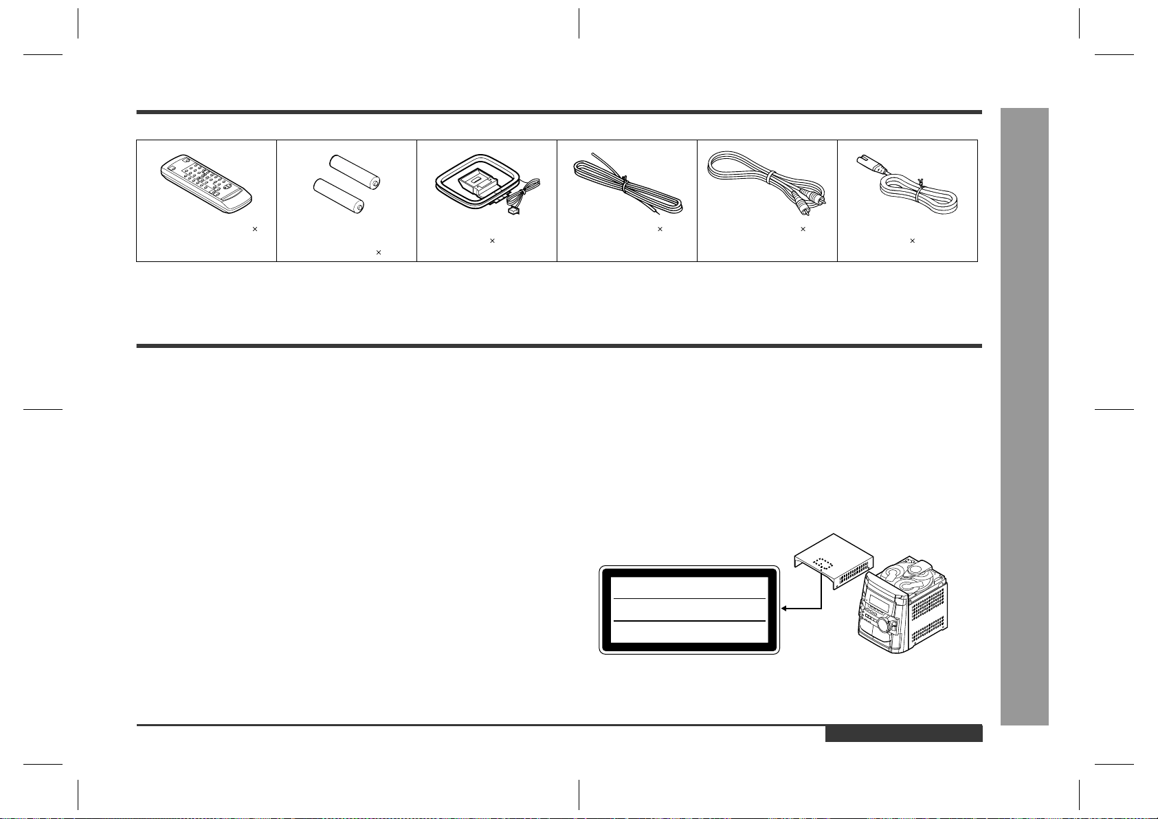
CD-BK110V/CD-BP99V
A
B
C
D
E
F
G
H
1
23456
Figure 8 CABINET EXPLODED VIEW (1/2)
– 8 –
Note: Only the unit and consumable parts are supplied as parts supply for the Tape mechanism.
601x3
202
202-1
202-2
610x2
Tape
Motor
MAIN BELT
FLYWHEEL
ASS'Y
TAPE 1
FLYWHEEL
ASS'Y
TAPE 2
FF/REW
ROLLER
ASS'Y
FF/REW
ROLLER
ASS'Y
BELT CONNECTION
207
607x9
610x3
PWB-F
223
IC904
IC902
Q905
608x6
Silicon
Grease
220
220
PWB-B
608x11
201-10
201-9
201-15
214
FL701
201
208
209
201-11
201-29
201-16
201-25
607
201-24
201-28
201-22
201-13
201-19
208
201-20
219x2
201-3
201-18
230
201-7
201-5
201-2
201-17
201-4
201-6
201-12
201-8
PWB-D
201-16
201-26
201-1
607
607
606x2
201-21
201-23
201-22
605x4
224x4
603x5
602x2
610x2
203
203-2
203-1
210
PWB-C
607
210-2
PT801
205
PWB-A
PWB-J
606x2
602x3
602x2
IC901
Silicon
Grease
606x2
604x2
258
258-1, 258-2, 258-3,
258-4, 258-5, 258-6,
258-7, 258-8, 258-9,
258-10, 258-11
262
210-1
262
201-14
CD-BK110V
ONLY
CD-BK110V
CD-BP99V
CD-BK110V
ONLY
CD-BK110V
ONLY
CD-BK110V
ONLY
CD-BK110V
CD-BP99V
CD-BK110V/CD-BP99V
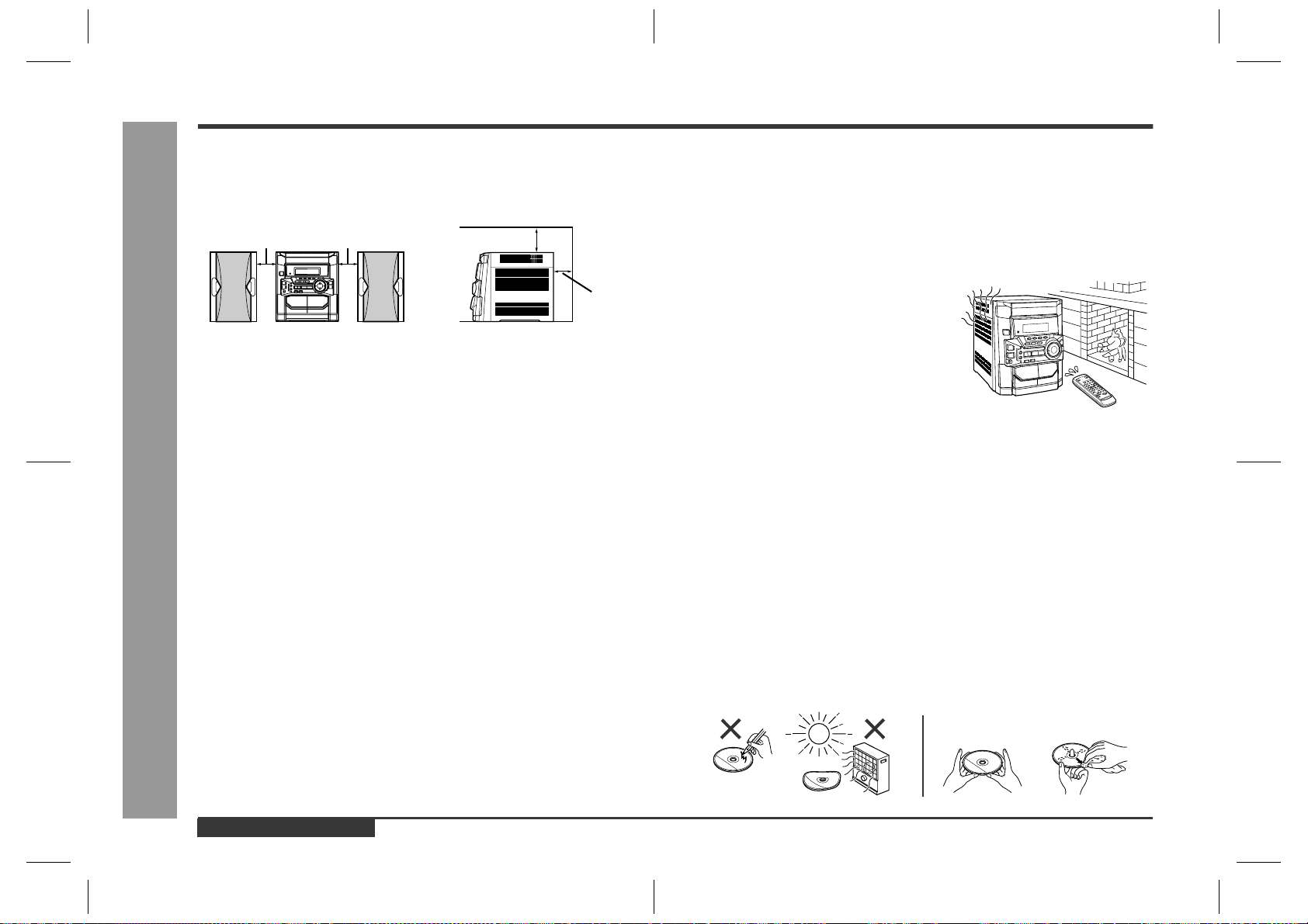
CD-BK110V/CD-BP99V
A
B
C
D
E
F
G
H
1
23456
Figure 9 CABINET EXPLODED VIEW (2/2)
250
229
236
254
CD
MECHANISM
252
204
609x2
609x2
231-4
231-5
231-2
231-1
237
611
261
231
SW3
SW2
SW1
232
225
M3
PWB-G
247
235
251
256
246
248
245
244
243x4
242
239
231-3
227
232x4
232
232
PWB-E
253
612
241
233
206
238
257
228
– 9 –
CD-BK110V/CD-BP99V

CD-BK110V/CD-BP99V
— M E M O —
– 10 –

CD-BK110V/CD-BP99V
COPYRIGHT 2001 BY SHARP CORPORATION
ALL RIGHTS RESERVED.
No part of this publication may be reproduced,
stored in a retrieval system, or transmitted in
any form or by any means, electronic, mechanical,
photocopying, recording, or otherwise, without
prior written permission of the publisher.
A0110-831DS•HA•M
EX
Printed in Japan
©
SHARP CORPORATION
AV Systems Group
Audio Systems Division
Higashihiroshima, Hiroshima 739-0192, Japan