□ Normal □ Internal Use Confidential □ Restricted Confidential
1
/
70
Product
Name:
I
M
Q
8
F4
module
Author: Wistron NeWeb Corporation
Revision: 1.0
Revision Date: 2026/01/15
Product Technical Specifications & Design guide
HW
Design
Guidelines
□ Normal □ Internal Use Confidential □ Restricted Confidential
2
/
70
Contact Information
Technical Support website https://SupportIoT.wnc.com.tw
Company Website www.wnc.com.tw
Revision History
Rev. # Author Summary of Changes Date
1.0 WNC First release 2026/01/15
1.1 WNC Modify module’s picture 2026/04/23
© WNC Corporation
THIS DOCUMENT AND THE INFORMATION CONTAINED HEREIN IS PROPRIETARY AND IS THE
EXCLUSIVE PROPERTY OF WNC AND SHALL NOT BE DISTRIBUTED, REPRODUCED, OR
DISCLOSED IN WHOLE OR IN PART WITHOUT PRIOR WRITTEN PERMISSION FROM WNC.
LIMITATION OF LIABILITY
THIS DOCUMENT AND THE INFORMATION CONTAINED HEREIN IS PURELY FOR DESIGN
REFERENCE AND SUBJECT TO REVISION BY WNC AT ANY TIME. NOTHING IN THIS
DOCUMENT SHALL BE CONSTRUED AS GRANTING ANY WARRANTY OR RIGHT TO USE THE
MATERIAL CONTAINED HEREIN WITHOUT WNC’S PRIOR EXPRESS WRITTEN CONSENT. WNC
SHALL NOT BE LIABLE FOR ANY USE, APPLICATION OR DEVELOPMENT DERIVED FROM THE
MATERIAL WITHOUT SUCH PRIOR EXPRESS WRITTEN CONSENT.

HW
Design
Guidelines
□ Normal □ Internal Use Confidential □ Restricted Confidential
3
/
70
Contents
Contact Information ............................................................................................................................. 2
Revision History ................................................................................................................................... 2
Contents .............................................................................................................................................. 3
1. Introduction ................................................................................................................................. 6
1.1. Abbreviation ............................................................................................................................... 6
1.2. Features ...................................................................................................................................... 7
2. Electrical Specifications ................................................................................................................ 9
2.1. Host interface pin assignments .................................................................................................. 9
2.1.1. LGA Pad Diagram ........................................................................................................... 9
2.1.2. Pin Assignments ........................................................................................................... 10
2.2. Power supply ............................................................................................................................ 19
2.3. USB interface ............................................................................................................................ 20
2.4. SGMII interface ......................................................................................................................... 22
2.5. UIM interface ............................................................................................................................ 23
2.6. Control interface ....................................................................................................................... 27
2.6.1. Power-on Signal ........................................................................................................... 27
2.6.2. Wake-up interface ....................................................................................................... 28
2.6.3. Reset Signal .................................................................................................................. 29
2.6.4. WWAN state Signal ...................................................................................................... 30
2.6.5. Emergency download interface ................................................................................... 30
2.7. Digital interface ........................................................................................................................ 31
2.7.1. JTAG Interface .............................................................................................................. 31
2.7.2. SPI Master Interface .................................................................................................... 32

HW
Design
Guidelines
□ Normal □ Internal Use Confidential □ Restricted Confidential
4
/
70
2.7.3. PCM Interface .............................................................................................................. 32
2.7.4. I2S Interface ................................................................................................................. 34
2.7.5. I2C Interface ................................................................................................................ 36
2.7.6. UART Interface ............................................................................................................. 36
2.7.7. ADC Interface ............................................................................................................... 37
2.7.8. Secure digital interfaces .............................................................................................. 37
3. RF Specifications ........................................................................................................................ 39
3.1. RF connections .......................................................................................................................... 39
3.2. Interference and sensitivity ...................................................................................................... 40
3.3. GNSS external circuit design ..................................................................................................... 42
3.4. RF Specification ......................................................................................................................... 44
3.4.1 Band support ............................................................................................................... 44
3.4.2 Bandwidth support ...................................................................................................... 45
3.4.3 RF Transmit Specification ............................................................................................ 45
3.4.4 RF Receiver Specification ............................................................................................. 46
3.4.5 GNSS Receiver Specification ........................................................................................ 50
4. Power ........................................................................................................................................ 51
4.1. Power consumption .................................................................................................................. 51
5. Software Interface ..................................................................................................................... 53
5.1. Support tools ............................................................................................................................ 53
5.2. USB interface ............................................................................................................................ 53
6. Mechanical and Environmental Certifications ............................................................................. 54
6.1. PCBA Form Factor ..................................................................................................................... 54
6.2. Module orientation .................................................................................................................. 57
6.3. Reflow ....................................................................................................................................... 58

HW
Design
Guidelines
□ Normal □ Internal Use Confidential □ Restricted Confidential
5
/
70
6.4. PCB pad design ......................................................................................................................... 59
6.5. Labeling ..................................................................................................................................... 60
6.6. SMT Voids control..................................................................................................................... 61
6.6.1. Mother board PCB thickness ....................................................................................... 61
6.6.2. Stencil design ............................................................................................................... 61
6.7. Thermal considerations ............................................................................................................ 62
7. Regulatory Compliance and Certification .................................................................................... 63
7.1. Certification testing .................................................................................................................. 63
8. Packaging .................................................................................................................................. 64
8.1. Tape-and-Reel Package ............................................................................................................ 64
8.2. Single Packaging for Samples.................................................................................................... 66
8.3. MSL level ................................................................................................................................... 66
9. Safety Recommendation ............................................................................................................ 67
10. Warning ..................................................................................................................................... 68
HW
Design
Guidelines
□ Normal □ Internal Use Confidential □ Restricted Confidential
6
/
70
1. Introduction
The IMQ8F4 modules are LTE modems which incorporate an application CPU subsystem and
peripheral interfaces and functions uniquely designed to address the
power/performance/cost requirements of IoT and M2M applications. The CPU is based on
Qualcomm’s MDM architecture which offers OFDMA-related software based signal
processing capabilities that significantly exceed traditional communications ARM cores.
IMQ8F4 modules provide a variety of interfaces including USB 2.0, SGMII, SPI, UART, PCM,
I2C, UIM & SDIO.
1.1. Abbreviation
Table 1. Abbreviation
Abbreviation Definition
AC Alternating Current
DC Direct Current
ETSI European Telecommunications Standards Institute
GND Ground
GPS Global Positioning System
GNSS Any single or combined satellite navigation system (GPS,
GLONASS and combined GPS/GLONASS)
GPIO General Purpose Input Output
I/O Input/Output
IoT Internet of Things
I2C Inter-Integrated Circuit
LGA Land Grid Array
LTE Long Term Evolution
Mbps Megabits per second
MIPS Millions of Instructions Per Second
N/A Not/Applicable
OS Operating System
PC Personal Computer
PCM Pulse Code Modulation
HW
Design
Guidelines
□ Normal □ Internal Use Confidential □ Restricted Confidential
7
/
70
PIN Personal Identification Number
SIM Subscriber Identity Module
SMA Surface Mount Antenna
SPI Serial Peripheral Interface
UART Universal Asynchronous Receiver-Transmitter
UIM User Identity Module
USB Universal Serial Bus
Vref Voltage reference
WCDMA Wideband Code Division Multiple Access
WNC WNC Corporation
1.2. Features
This section lists main features of IMQ8F4 module support. For wireless technology and
band support information among different modules, please refer to table2 for detail
information.
Table 2. IMQ8F4 Series module overview
Module
Category
LTE WCDMA
GNSS Temperature Grade
B2/4/5/12/13/25/26/66/71
B2/5
IMQ8QF4
4 √ √ √ Industrial
Note: 1.Refer to section6.6 for more information about industrial grade.
2. “√” indicates supporting. “×” indicates not supporting.

HW
Design
Guidelines
□ Normal □ Internal Use Confidential □ Restricted Confidential
8
/
70
Feature list:
LTE 3GPP release 10 without Carrier Aggregation
IMQ8F4: 3GPP, LTE Cat. 4 with 150/50 Mbps for DL/UL
Supports LTE B2/4/5/12/13/25/26/66/71
Supports WCDMA B2/5, 3GPP release 8
Ultra-high-performance Cortex A7 microprocessor
Modem subsystem (MSS)
Resource and power management (RPM) subsystem
Optimized for M2M and IoT markets
Interfaces
– HS USB 2.0 with integrated PHY
– SGMII interface
– Dual UART interfaces (4 bit and 2 bit) for data transfer and diagnostic tools
– SDC1/First SPI interface
– I2C/Second SPI interface
– USIM interface
– GPIOs
– ADC
– PCM/I2S
– JTAG interface
HW
Design
Guidelines
□ Normal □ Internal Use Confidential □ Restricted Confidential
9
/
70
2. Electrical Specifications
2.1. Host interface pin assignments
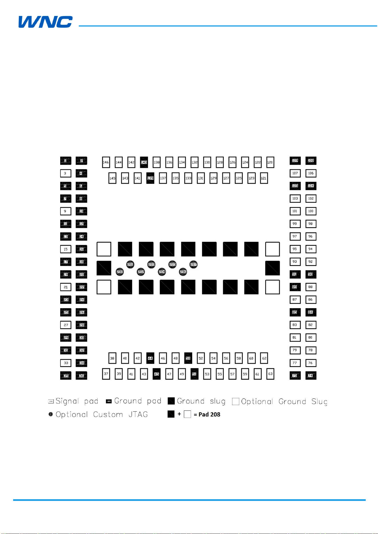
2.1.1. LGA Pad Diagram
Figure 1. LGA pad diagram (top view)
HW
Design
Guidelines
□ Normal □ Internal Use Confidential □ Restricted Confidential
10
/
70
2.1.2. Pin Assignments
I/O type description:
AO : Analog Output
AI : Analog Input
DO : Digital Output
DI : Digital Input
Table 3. Pin interface family
Interface Family
Signal Description I/O
RF Interfaces
RF_2 Diversity antenna AI
RF_GNSS Reserved for GNSS receiver AI
RF_1 Main Antenna AI/AO
User Identity Module
UIM_VCC Power source for UIM AO
UIM_DATA Data in/out DI/DO
UIM_CLK Clock signal DO
UIM_RESET Reset signal DO
UIM_DETECT UIM Detect signal DI/DO
Data Interfaces- USB 2.0
USB_HS_DP USB Data Positive DI/DO
USB Detect USB Detect DI
USB_HS_DM USB Data Negative DI/DO
Data Interfaces- SGMII
SGMII_RX_P SGMII receive - plus DI
SGMII_RX_M SGMII receive - minus DI
SGMII_TX_P SGMII transmit - plus DO
SGMII_TX_M SGMII transmit - minus DO
SGMII_MDIO SGMII Management data DI/DO
SGMII_MDC SGMII Management data clock DI/DO
Data Interfaces- UART1
UART1_CTS_N Clear To Send for UART 1 DI
UART1_RFR_N Ready for receive for UART1 DO
UART1_RX Receive for UART 1 DI
UART1_TX Transmit for UART 1 DO
Data Interfaces- UART2

HW
Design
Guidelines
□ Normal □ Internal Use Confidential □ Restricted Confidential
11
/
70
UART2_RX Receive for UART 2 DI
UART2_TX Transmit for UART 2 DO
Data Interfaces- I2C/2nd_ SPI
I2C_SDA Data in/out DI/DO
2nd_SPI_EN_1 2nd_SPI chip select DO
I2C_SCL Clock signal DO
2nd_SPI_CLK 2nd_SPI serial clock DO
SPI_MOSI 2nd_SPI master out slave in DO
NC NC -
SPI_MISO 2nd_SPI master in slave out DI
Data Interfaces- SDC1/1st_SPI
SDC1_DATA_3 SDC1_DATA_3 DI/DO
1st_SPIM_MOSI 1st_SPI master out slave in DO
SDC1_DATA_2 SDC1_DATA_2 DI/DO
1st_SPIM_MISO 1st_SPI master in slave out DI
SDC1_DATA_1 SDC1_DATA_1 DI/DO
1st_SPIM_EN_1 1st_SPI chip select DO
SDC1_DATA_0 SDC1_DATA_0 DI/DO
1st_SPIM_CLK 1st_SPI serial clock DO
SDC1_CMD SDC1_CMD DI/DO
SDC1_CLK SDC1_CLK DO
Module Control and State Interfaces
WWAN_STATE Wireless WAN Radio State DO
POWER_ON Power On the module DI
WAKEUP_OUT Module wakes up host DO
WAKEUP_IN Host wakes up module DI
RESET Reset the module DI
Power and Ground
VREF Voltage Reference Output AO
VCC Main Power AI
GND GND AI
General Purpose
GPIO Digital I/O DI/DO
ADC_CONVENTOR ADC_CONVENTOR AI
AUDIO- PCM/I2S
PCM_DIN PCM_DIN DI
HW
Design
Guidelines
□ Normal □ Internal Use Confidential □ Restricted Confidential
12
/
70
I2S_DATA0 I2S_DATA0 DI/DO
PCM_DOUT PCM_DOUT DO
I2S_DATA1 I2S_DATA1 DI/DO
PCM_CLK PCM_CLK DO
I2S_SCK I2S_SCK DO
PCM_SYNC PCM_SYNC DO
I2S_WS I2S_WS DO
RFU- RFU
RFU Reserved For Future Use -
Debug- JTAG
JTAG_SRST_N JTAG reset for debug DI
JTAG_TCK JTAG clock input DI
JTAG_TDI JTAG data input DI
JTAG_TDO JTAG data output DO
JTAG_TMS JTAG mode select input DI
JTAG_TRST_N JTAG reset DO
PS_HOLD PS_HOLD DI
Debug- Force_USB_BOOT
Force_USB_BOOT_CON
FIG Force USB BOOT CONFIG DI
Table 4. Pin Assignments
Pin
No.
Modem
mod
e Host Mode
Voltage Level (V)
Min. Typ. Max.
1 GND GND - 0 -
2 GND GND - 0 -
3 NC NC - - -
4 GND GND - 0 -
5 GND GND - 0 -
6 GND GND - 0 -
7 GND GND - 0 -
8 GND GND - 0 -
9 RF_GNSS RF_GNSS - - -
10 GND GND - 0 -
11 GND GND - 0 -
12 GND GND - 0 -
13 GND GND - 0 -

HW
Design
Guidelines
□ Normal □ Internal Use Confidential □ Restricted Confidential
13
/
70
14 GND GND - 0 -
15 RF_1 RF_1 - - -
16 GND GND - 0 -
17 GND GND - 0 -
18 GND GND - 0 -
19 GND GND - 0 -
20 GND GND - 0 -
21 RF_2 RF_2 - - -
22 GND GND - 0 -
23 GND GND - 0 -
24 GND GND - 0 -
25 GND GND - 0 -
26 GND GND - 0 -
27 NC NC - - -
28 GND GND - 0 -
29 GND GND - 0 -
30 GND GND - 0 -
31 GND GND - 0 -
32 GND GND - 0 -
33 NC NC - - -
34 GND GND - 0 -
35 GND GND - 0 -
36 GND GND - 0 -
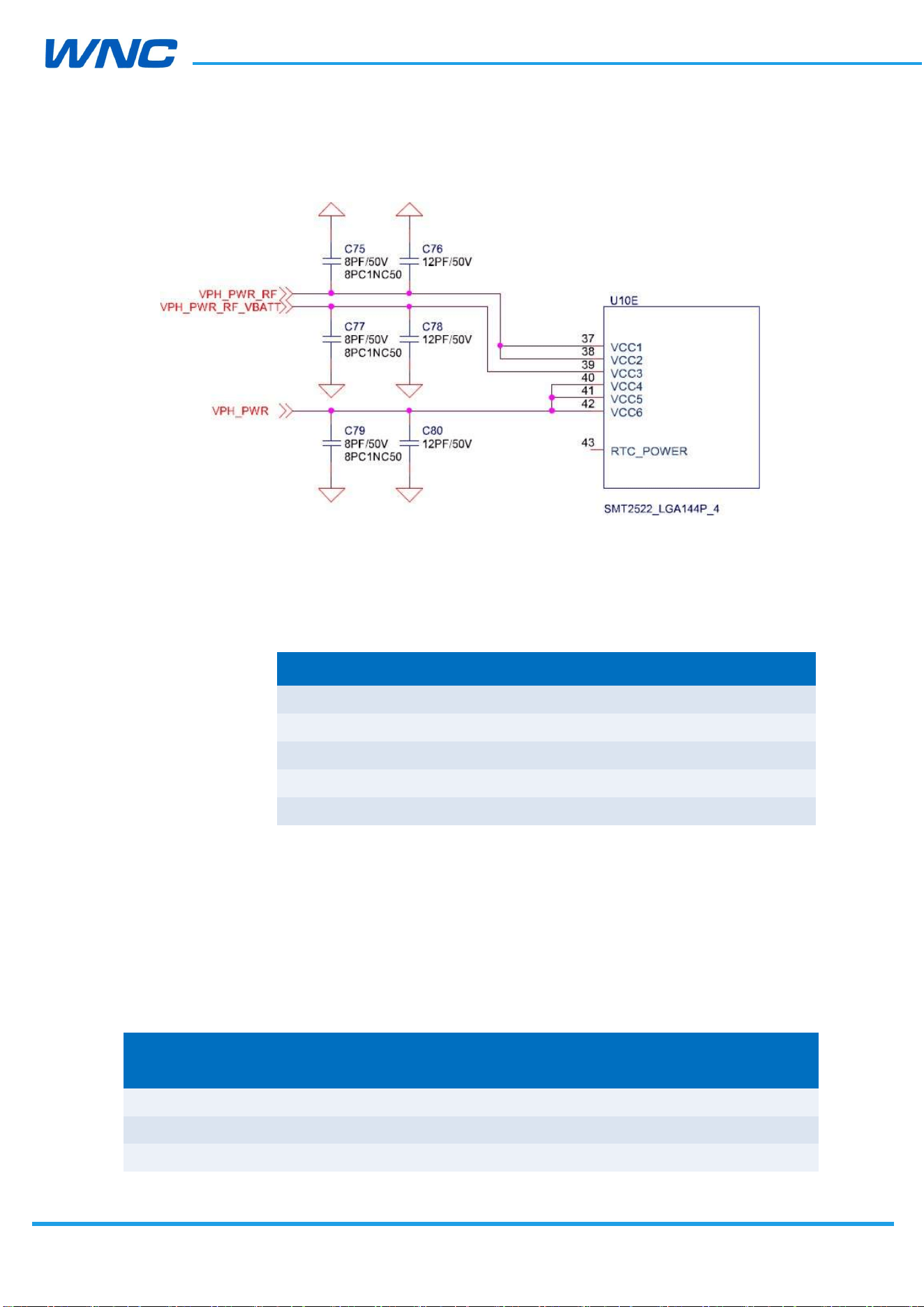
37 VCC1 VCC1 3.3 3.8 4.2
38 VCC2 VCC2 3.3 3.8 4.2
39 VCC3 VCC3 3.3 3.8 4.2
40 VCC4 VCC4 3.3 3.8 4.2
41 VCC5 VCC5 3.3 3.8 4.2
42 VCC6 VCC6 3.3 3.8 4.2
43 NC NC - - -
44 GND GND - 0 -
45 GND GND - 0 -
46 PCM_SYNC/GPIO46 PCM_SYNC/GPIO46 1.7 1.8 1.9
47 PCM_DIN/GPIO47 PCM_DIN/GPIO47 1.7 1.8 1.9
48 PCM_DOUT/GPIO48
PCM_DOUT/GPIO48 1.7 1.8 1.9
49 PCM_CLK/GPIO49 PCM_CLK/GPIO49 1.7 1.8 1.9

HW
Design
Guidelines
□ Normal □ Internal Use Confidential □ Restricted Confidential
14
/
70
50 GND GND - 0 -
51 GND GND - 0 -
52 GPIO01/Force USB
BOOT Config
*4
GPIO01/Force USB
BOOT Config*
4
1.7 1.8 1.9
53 GPIO02 GPIO02 1.7 1.8 1.9
54 GPIO03 GPIO03 1.7 1.8 1.9
55 GPIO04 GPIO04 1.7 1.8 1.9
56 NC SGMII_TX_P
*1
- - -
57 NC SGMII_TX_M
*1
- - -
58 NC SGMII_RX_P
*1
- - -
59 NC SGMII_RX_M
*1
- - -
60 I2C_SDA I2C_SDA/
2nd_SPI_EN_1
1.7 1.8 1.9
61 I2C_SCL I2C_SCL/
2nd_SPI_CLK
1.7 1.8 1.9
62 NC 2nd_SPI_MOSI 1.7 1.8 1.9
63 NC 2nd_SPI_MISO 1.7 1.8 1.9
74 GND GND - 0 -
75 GND GND - 0 -
76 RFFE1_DATA RFFE1_DATA - - -
77 RFFE1_CLK RFFE1_CLK - - -
78 NC NC - - -
79 NC NC - - -
80 UART1_CTS (UART
1)
UART1_CTS (UART 1) 1.7 1.8 1.9
81 UART1_RTS (UART
1)
UART1_RTS (UART 1) 1.7 1.8 1.9
82 UART1_RX (UART 1)
UART1_RX (UART 1) 1.7 1.8 1.9
83 UART1_TX (UART 1)
UART1_TX (UART 1) 1.7 1.8 1.9
84 GND GND - 0 -
85 GND GND - 0 -
86 USB_Dp
*2
USB_Dp
*2
- - -
87 USB Detect
*3
USB Detect
*3
1.7 1.8 1.9
88 USB_Dn
*2
USB_Dn
*2
- - -
89 GND GND - 0 -
90 GND GND - 0 -
91 GND GND - 0 -
92 NC GPIO92 1.7 1.8 1.9

HW
Design
Guidelines
□ Normal □ Internal Use Confidential □ Restricted Confidential
15
/
70
93 GPIO93 GPIO93 1.7 1.8 1.9
94 GPIO94 GPIO94 1.7 1.8 1.9
95 GPIO95 GPIO95 1.7 1.8 1.9
96 GPIO96 GPIO96 1.7 1.8 1.9
97 GPIO97 GPIO97 1.7 1.8 1.9
98 NC GPIO98 1.7 1.8 1.9
99 NC NC - - -
100 NC NC - - -
101 NC GPIO101 1.7 1.8 1.9
102 NC GPIO102 1.7 1.8 1.9
103 NC EPHY_RST_N 1.7 1.8 1.9
104 GND GND - 0 -
105 GND GND - 0 -
106 UART2_RX (UART 2)
UART2_RX (UART 2)
1.7 1.8 1.9
107 UART2_TX (UART 2)
UART2_TX (UART 2)
1.7 1.8 1.9
108 GND GND - 0 -
109 GND GND - 0 -
120 NC SGMII_MDC
*1
- - -
121 NC SGMII_MDIO
*1
- - -
122 AD Converter AD Converter 0.1 - 1.7
123 NC SDC1_CMD 1.7 1.8 1.9
124 NC SDC1_CLK 1.7 1.8 1.9
125 1st_SPI_MOSI SDC1_DATA_3/
1st _SPIM_MOSI
1.7 1.8 1.9
126 1st _SPI_MISO SDC1_DATA_2/
1st _SPIM_MISO
1.7 1.8 1.9
127 1st _SPI_EN_1 SDC1_DATA_1/
1st _SPIM_EN_1
1.7 1.8 1.9
128 1st _SPI_CLK SDC1_DATA_0/
1st _SPIM_CLK
1.7 1.8 1.9
129 GPIO05 GPIO05 1.7 1.8 1.9
130 GPIO06 GPIO06 1.7 1.8 1.9
131 GPIO07 GPIO07 1.7 1.8 1.9
132 GPIO08 EPHY_INT_N/GPIO08
1.7 1.8 1.9
133 UIM_VCC UIM_VCC 1.7/2.7 1.8/3.0 1.9/3.3
134 UIM_DATA UIM_DATA 1.7/2.7 1.8/3.0 1.9/3.3

HW
Design
Guidelines
□ Normal □ Internal Use Confidential □ Restricted Confidential
16
/
70
135 UIM_CLK UIM_CLK 1.7/2.7 1.8/3.0 1.9/3.3
136 UIM_RESET UIM_RESET 1.7/2.7 1.8/3.0 1.9/3.3
137 UIM_DETECT UIM_DETECT 1.7 1.8 1.9
138 NC NC - - -
139 GND GND - 0 -
140 GND GND - 0 -
141 WWAN_STATE WWAN_STATE 1.7 1.8 1.9
142 POWER_ON POWER_ON 1.7 1.8 1.9
143 WAKEUP_OUT
*5
WAKEUP_OUT
*5
1.7 1.8 1.9
144 WAKEUP_IN WAKEUP_IN 1.7 1.8 1.9
145 RESET RESET 1.7 1.8 1.9
146 VREF VREF 1.7 1.8 1.9
200 JTAG_SRST_N JTAG_SRST_N 1.7 1.8 1.9
201 JTAG TCK JTAG TCK 1.7 1.8 1.9
202 JTAG TDI JTAG TDI 1.7 1.8 1.9
203 JTAG TDO JTAG TDO 1.7 1.8 1.9
204 JTAG_TMS JTAG_TMS 1.7 1.8 1.9
205 JTAG TRST_N JTAG TRST_N 1.7 1.8 1.9
206 PS_HOLD PS_HOLD 1.7 1.8 1.9
207 NC NC - - -
Notes:
*1. Refer to SGMII standard for more electronic characteristics.
*2. Refer to section 2.3, for more information please check USB2.0 standard
*3. Pull pin87 USB detect to VREF with a 100k resistor to enable module USB, pull
pin87 low to disable module USB, CPU USB PHY consumes some current when
USB is enabled.
*4. Do not pull pin52 to high before the system boot process is complete.
*5. Do not pull pin143 WAKEUP_OUT to high; otherwise boot will fail.
*6. Leave unused pins floating
*7. Reserve test points on pin52/86/88/106/107 for debug purpose if possible.
*8. If voltage level of digital I/O from the other side is not compatible with module,
level shifter is recommended to transfer the voltage level to 1.8V.
HW
Design
Guidelines
□ Normal □ Internal Use Confidential □ Restricted Confidential
17
/
70
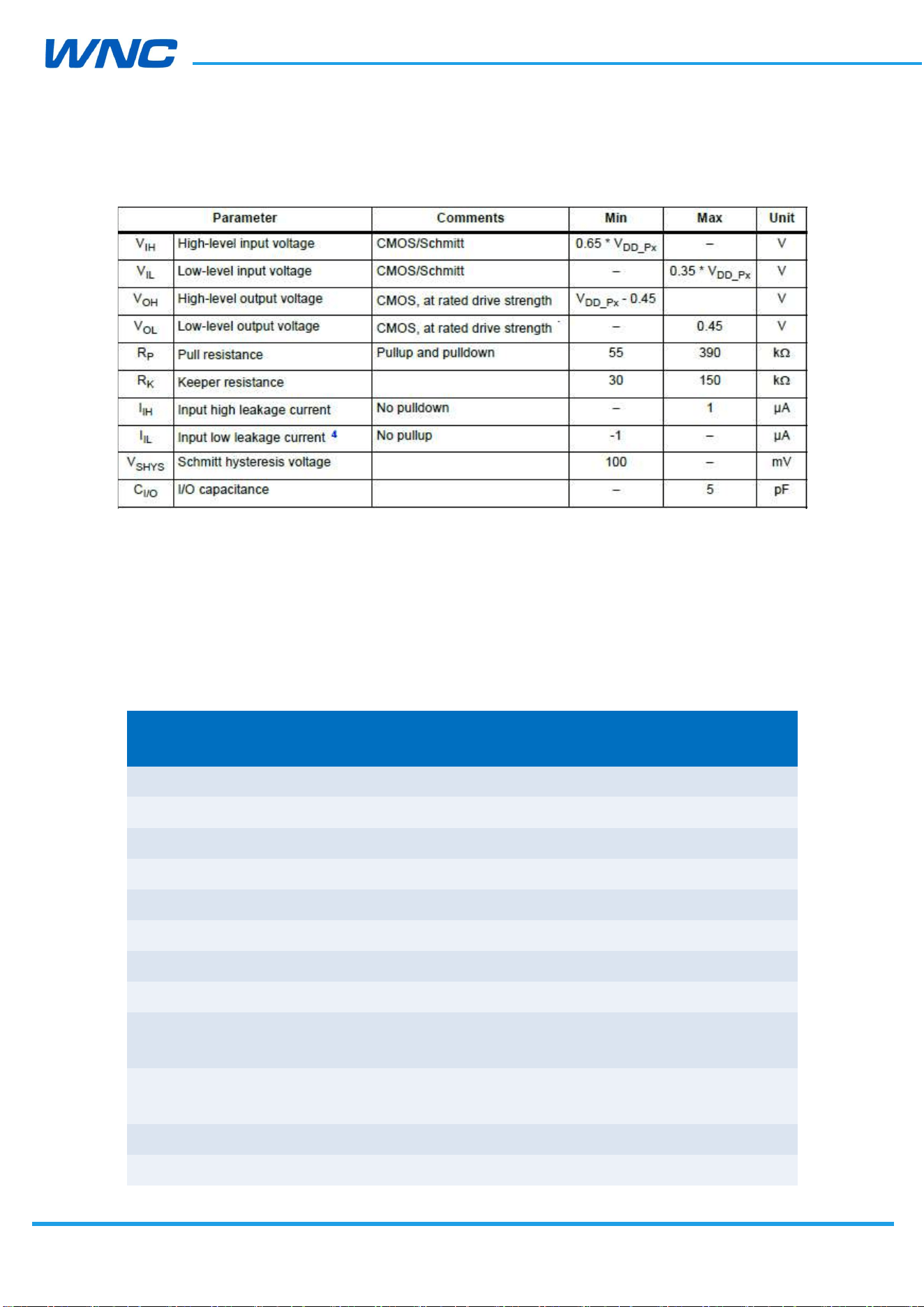
Table 5. Digital I/O characteristics
Below is the I/O default setting table to describe the level. It’s recommended to follow the
pulling High or Low to choose a suitable GPIO for application.
PU: Pull Up.
PD: Pull Down
NP: Non-Pull
Table 6. I/O default setting table
Pin
No.
Signal Name Type
Default setting in
Normal mode
46 PCM_SYNC/GPIO46 DI /DO PD
47 PCM_IN/GPIO47 DI /DO PD
48 PCM_OUT/GPIO48 DI /DO PD
49 PCM_CLK/GPIO49 DI /DO PD
52 GPIO01 DI/DO PD
53 GPIO02 DI/DO PD
54 GPIO03 DI/DO PD
55 GPIO04 DI/DO PD
60 I2C_SCL/
2nd_SPI_CLK
DI/DO PD
61 I2C_SDA/
2nd_SPI_EN_1
DI/DO PD
62 2nd_SPI_MOSI DI/DO PD
63 2nd_SPI_MISO DI/DO PD

HW
Design
Guidelines
□ Normal □ Internal Use Confidential □ Restricted Confidential
18
/
70
80 UART1_CTS (UART1)
DI/DO PD
81 UART1_RTS (UART1)
DI/DO PD
82 UART1_RX (UART1) DI/DO PD
83 UART1_TX (UART1) DI/DO PD
92 GPIO92 DI/DO PD
93 GPIO93 DO NP
94 GPIO94 DI/DO PD
95 GPIO95 DI/DO PD
96 GPIO96 DI/DO PD
97 GPIO97 DI/DO PD
98 GPIO98 DI/DO PU
101 GPIO101 DI/DO PD
102 GPIO102 DI/DO PD
103 GPIO103 DI/DO PD
106 UART2_RX (UART2) DI/DO PD
107 UART2_TX (UART2) DI/DO PD
120 GPIO120 DI/DO PD
123 GPIO123 DI/DO PD
124 GPIO124 DI/DO NP
125 SPIM_MOSI DI/DO PD
126 SPIM_MISO DI/DO PD
127 SPIM_EN DI/DO PD
128 SPIM_CLK DI/DO PD
129 GPIO05 DI/DO PD
130 GPIO06 DI/DO PD
131 GPIO07 DI/DO PU
132 GPIO08 DI/DO PD
141 WWAN_STATE DI/DO PD
143 WAKEUP_OUT DI/DO PD
HW
Design
Guidelines
□ Normal □ Internal Use Confidential □ Restricted Confidential
19
/
70
2.2. Power supply
LTE module power input is VCC. The internal power chipset will transfer VCC to other power
level.
Table 7. Power supply voltage level
Power Pin Name
Pads Description
Voltage Level (V)
Min.
Typ.
Max.
VCC VCC1 to VC
C6
Nos. 37 to
42
Main Power Supply
3.3 3.8 4.2
The IMQ8F4 include an integrated power manager enabling single and direct voltage supply
from the battery, reducing the overall bill of materials. The typical voltage 3.8V is
recommended.
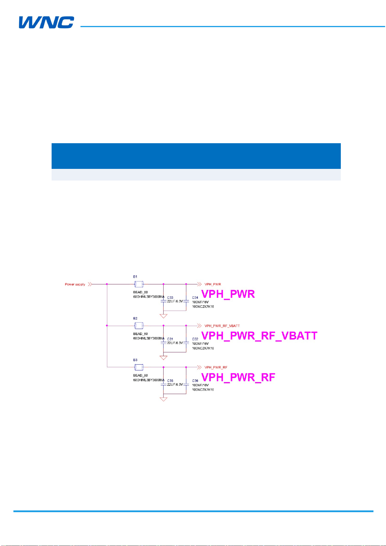
Schematic suggestion: Must to separate module power supply to three paths to keep
power clean as below for TX spurious performance. The VPH_PWR is for Baseband and RF
transceiver, the VPH_PWR_RF is for RF PA, the VPH_PWR_RF_VBATT is for RF PA control
circuit.
HW
Design
Guidelines
□ Normal □ Internal Use Confidential □ Restricted Confidential
20
/
70
Layout Suggestion: The 22μF, 0.1uF, 12pF and 8pF capacitors are required to place near
VCC pins as close as possible. Each power trace should possess
sufficient line width to withstand its respective current listed in the
table below:
Net Name Current Value
VCC(1–2) total 2A
VCC(3) total 100mA
VCC(4–6) total 1A
UIM_VCC 150 mA
VREF 300 mA
2.3. USB interface
The IMQ8F4 modules comply with USB 2.0 high-speed protocol. The USB input/output lines
follow USB 2.0 specifications.
Table 8. Signals of the USB interface
Name Description
Input/Output
(Direction to module)
Voltage Level (V)
Min. Typ.
Max.
D+
USB data positive (low-/full-speed)
Input High 2 3.3 3.6
HW
Design
Guidelines
□ Normal □ Internal Use Confidential □ Restricted Confidential
21
/
70
Input Low 0
0.8
Output High 2.8 3.3 3.6
Output Low
0.3
USB data positive (high-speed)
Input High 0.3
0.44
Input Low 0
0.01
Output High 0.36 0.38 0.44
Output Low 0
0.01
D–
USB data negative (low-/full-speed)
Input High 2 3.3 3.6
Input Low 0
0.8
Output High 2.8 3.3 3.6
Output Low
0.3
USB data negative (high-speed)
Input High 0.3
0.44
Input Low 0
0.01
Output High 0.36 0.38 0.44
Output Low 0
0.01
The layout design of this circuit on the carrier board should comply with the USB 2.0 high-
speed protocol.
Layout suggestion:
Differential impedance: 90 Ω
Space to other signals should be at least 20 mils
Intra-lane length difference should be less than 150 mils
Maximum length for each trace:150 mm
Signals lengths on modules are tuned as below:
Function Net Length (mil)
USB
USB_Dp 545.54
USB_Dn 503.04
HW
Design
Guidelines
□ Normal □ Internal Use Confidential □ Restricted Confidential
22
/
70
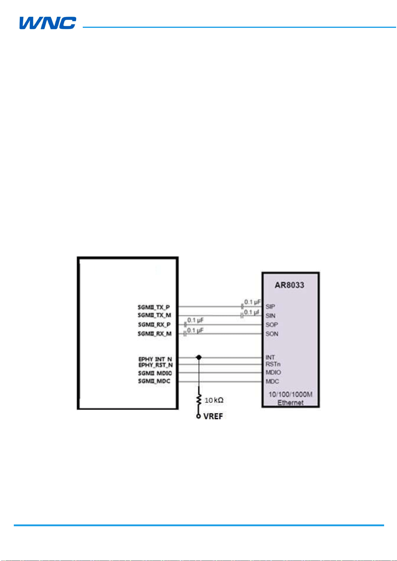
2.4. SGMII interface
The IMQ8F4 modules integrate Ethernet MAC with SGMII interfaces with the following key
features:
IEEE 802.3 compliance
Full duplex at 1 Gbps
Half/full duplex for 10/100 Mbps
Supports VLAN tagging
Supports IEEE 1588, Precision Time Protocol (PTP)
Can be used to connect to external Ethernet PHYs such as AR8033 or to an
external switch
The following figure illustrates an example of the additional logic connection between the
modules and the Ethernet chip. Refer to ENG-46158, Rev 1.8 for electrical and timing
specifications.
Figure 2. SGMII circuit example
Layout suggestion:
Differential impedance:100 Ω
Space to other signals: > 3x line width
Lane-to-lane space: > 3x line width
Intra-lane mismatch: < 0.7 mm
IMQ8F4
HW
Design
Guidelines
□ Normal □ Internal Use Confidential □ Restricted Confidential
23
/
70
Signal lengths on the modules are tuned as below:
Function Net Length (mil)
SGMII
SGMII_TX_P 617.11
SGMII_TX_M 642.13
SGMII_RX_P_C+SGMII_RX_P 661.40
SGMII_RX_M_C+SGMII_RX_M 675.06
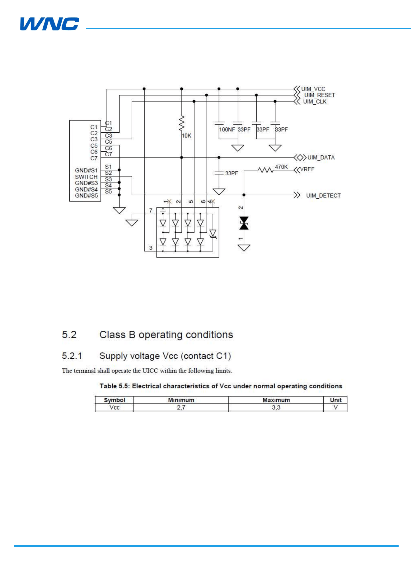
2.5. UIM interface
IMQ8F4 modules provide an UIM_DETECT input pin for UIM connector to detect UIM card.
When UIM card is present, UIM_DETECT should be high (1.8V). If UIM card is absent,
UIM_DETECT should be low. It’s required to pull UIM_DETECT to VREF with a 470k resistor.
A 0.1μF and a 33pF capacitor are recommended to place between UIM_VCC and Ground in
parallel. A 33pF capacitor is recommended to place between UIM_RESET, UIM_CLK and
UIM_DATA and Ground in parallel, see Figure5 for reference.
Electrostatic discharge (ESD) protection circuit is also recommended to place near the UIM
socket as close as possible, and the Ground pin of the ESD protection component must be
well connected to the Ground plane.
The following figure shows an example of UIM card circuit.
HW
Design
Guidelines
□ Normal □ Internal Use Confidential □ Restricted Confidential
24
/
70
Figure 3. UIM card circuit example
It’s highly suggested to make sure that SIM electrical characteristics can meet ETSI TS 102
221 requirement before going to certification like PTCRB. Refer to the following capture
from ETSI TS 102 221 section 5 for critical requirement:
HW
Design
Guidelines
□ Normal □ Internal Use Confidential □ Restricted Confidential
25
/
70
HW
Design
Guidelines
□ Normal □ Internal Use Confidential □ Restricted Confidential
26
/
70
HW
Design
Guidelines
□ Normal □ Internal Use Confidential □ Restricted Confidential
27
/
70
2.6. Control interface
This section describes the power-on/off, wake-up and reset interface on how to control the
module.
2.6.1. Power-on Signal
The POWER_ON is an active Low input signal used to enable or disable the module. Do not
toggle the PERST# pin during power-on. This signal has the highest priority over the
wakeup, the alarms signals, and the digital control pins.
There are three possible states of the module:
Module Power Off - VCC is not present.
Module Disabled - VCC is supplied, pull power-on signal be high.
Module Enabled - VCC is supplied, pull power-on signal be low to bootup.
The state transitions are defined as follows:
When voltage is applied to VCC, the module shall enter the Module Disabled
state.
HW
Design
Guidelines
□ Normal □ Internal Use Confidential □ Restricted Confidential
28
/
70
An input to the POWER_ON pin shall trigger the transition from the Module
Disabled to the Module Enabled state. See figure6, a low pulse(tlow > 0s) on
POWER_ON pad will enable the module after VCC is applied.
An input to the POWER_ON pin shall trigger the transition from the Module
Enabled to the Module Disabled state. See figure6, after power on, a low pulse
(tlow > 2s) on POWER_ON pin will disable (power-off) the module.
Figure 4. Power ON/OFF timming
2.6.2. Wake-up interface
In applications where power consumption is a major factor in performance metrics (such as
battery-operated sensors that are based on IOT/M2M modem solution and also include a
third party host), it is necessary to define a simple interface that will allow both the modem
and the host to be able to enter low power states whenever possible and the other side to
wake it up once required.
For example, if the host has no data to transmit or any other tasks, it may enter some low
power state according to its own capabilities and configurations. If during that period the
host is in a low power state and the modem suddenly receives data, it must wake-up the
host.
A similar requirement exists from the other side. For example, if the modem is in a low
power state and suddenly the host must transmit data, it must be able to wake-up the
modem.
The interface consists of two signals: One is driven by the host and received by the modem;
the other is driven by the modem and received by the host.
HW
Design
Guidelines
□ Normal □ Internal Use Confidential □ Restricted Confidential
29
/
70
Each side can wake the other side by toggling wakeup signal high and allowing the other
side to go to sleep when not needed by toggling it low.
“WAKEUP_IN” (Host: Output, Modem: Input):
– LOW: SoC does not require the MODEM (allowing it to sleep).
– HIGH: SoC requires the MODEM or acknowledges it is ready following a
wakeup request from the MODEM.
“WAKEUP_OUT” (Host: Input, Modem: Output):
– LOW: The MODEM does not require the Host (allowing it to sleep)
– HIGH: The MODEM requires the Host or acknowledges it is ready
following a wakeup request from the SoC.
When IMQ8F4 modules act as modem, keep WAKEUP_IN high before system boot process is
complete, after system boot, keep WAKEUP_IN low. WAKEUP_IN and WAKEUP_OUT
behavior of host mode will be discussed according to product specification.
2.6.3. Reset Signal
The Reset Signal is a hardware reset signal to control the system reset directly. You can
connect it to a key or a control signal. A low pulse (3s<tlow<8s) after power on will reset the
module, see figure7.
Figure 5. Reset Signals circuit
HW
Design
Guidelines
□ Normal □ Internal Use Confidential □ Restricted Confidential
30
/
70
2.6.4. WWAN state Signal
The WWAN state pin definition as below.
WWAN state pin output “high”
When device register to network, the WWAN state pin output “high”.
WWAN state pin output “low”
When device not to register to network, the WWAN state pin output “low”.
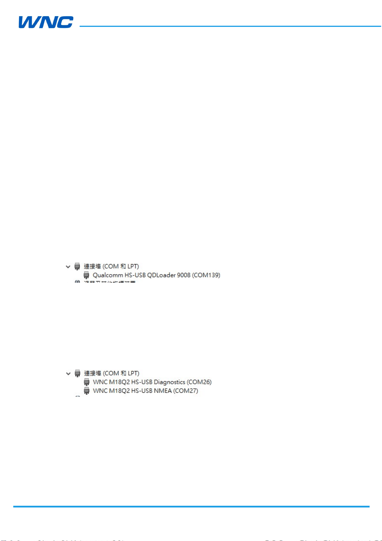
2.6.5. Emergency download interface
Two ways can enter emergency download, hardware and software path.
Hardware path to enter EDL:
- Pull Force_USB_BOOT (pin52) to VREF (pin146) until power on module and pull low
power-on signal. Success if device manager shows QDLoader 9008.
- Send Reboot once complete firmware download.
- Exit emergency download by power cycling VCC on module.
Software path to enter EDL:
Module bootup completely, check interfaces are generated.
Follow software flow by WNC document- Build & download open source FW SOP .
Success if device manager shows QDLoader 9008.
HW
Design
Guidelines
□ Normal □ Internal Use Confidential □ Restricted Confidential
31
/
70
2.7. Digital interface
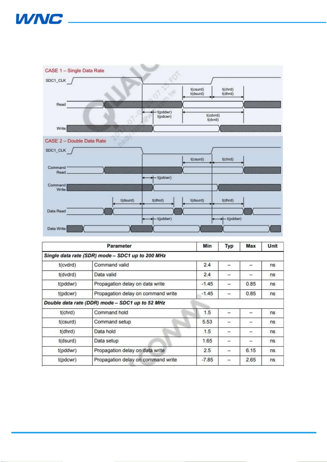
This section provides required AC timing information related to module digital interfaces.
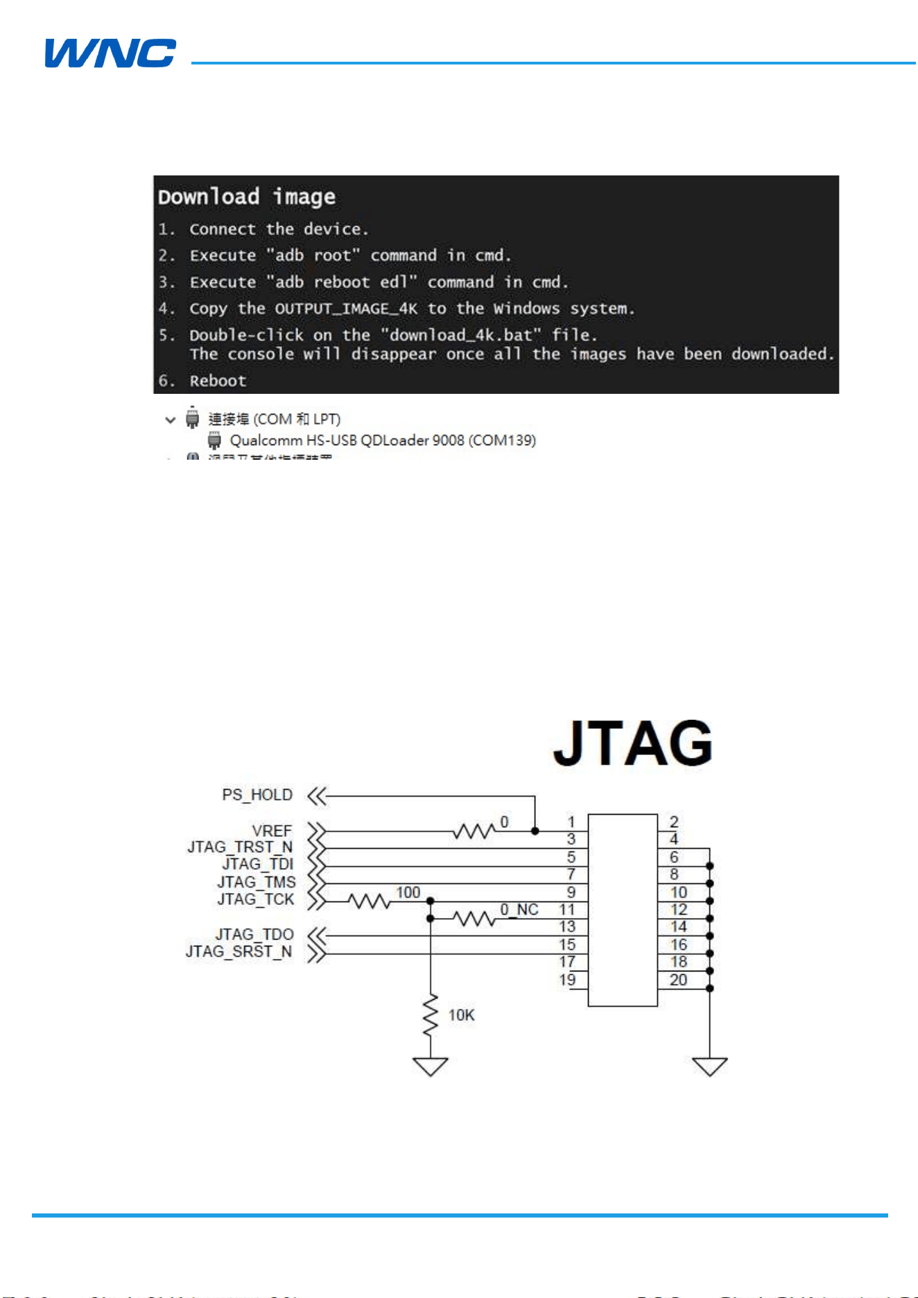
2.7.1. JTAG Interface
IMQ8F4 provide one JTAG interface, leave JTAG pins floating if not used.
Figure 6. JTAG schematic (example)
HW
Design
Guidelines
□ Normal □ Internal Use Confidential □ Restricted Confidential
32
/
70
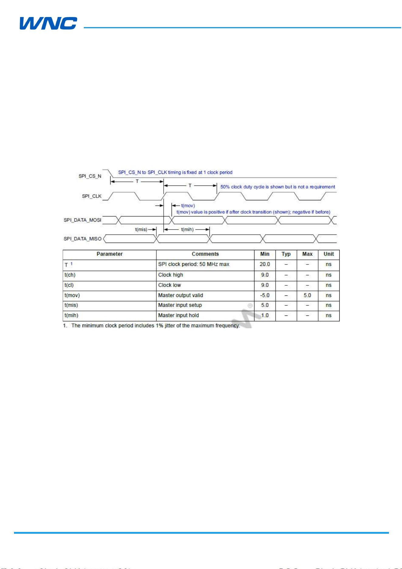
2.7.2. SPI Master Interface
SPIM_CLK – Output clock
SPIM_CS – Output, chip-select
SPIM_MOSI – Output, data to slave
SPIM_MISO – Input, data from slave
Timing
Figure 7. SPI timing parameters
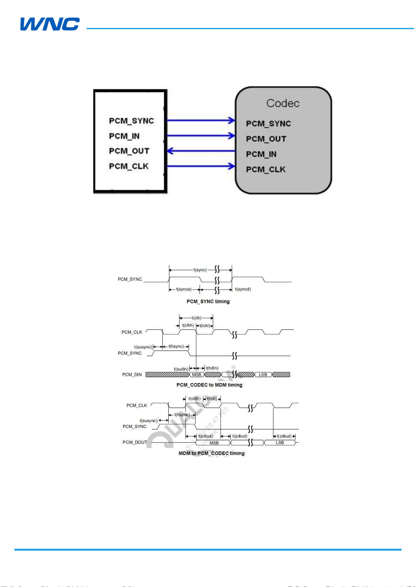
2.7.3. PCM Interface
IMQ8F4 modules provide one PCM master digital audio interface. Keep PCM signal traces far
away from noise and radiating signal on PCB
HW
Design
Guidelines
□ Normal □ Internal Use Confidential □ Restricted Confidential
33
/
70
Figure 8. PCM connection (example)
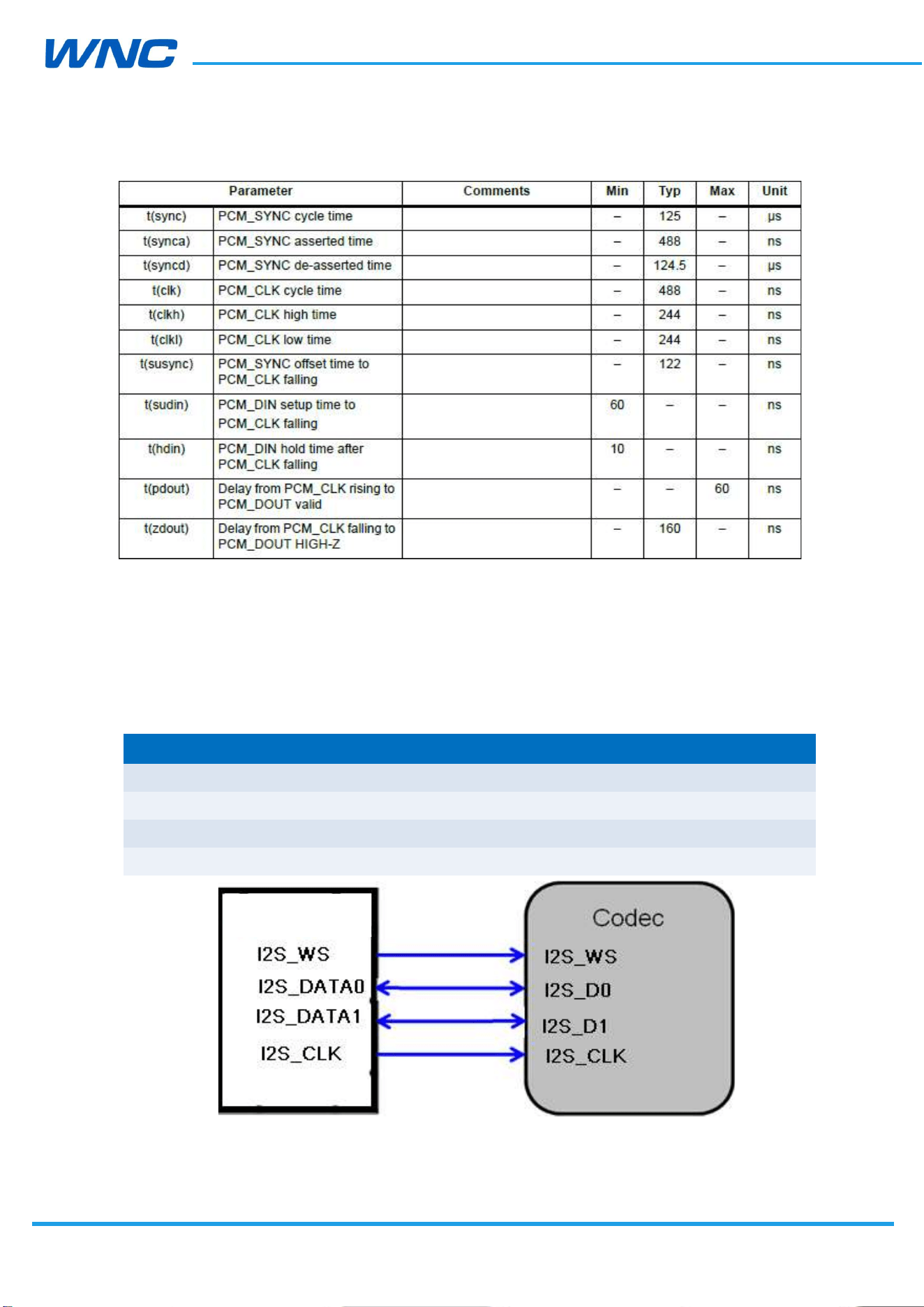
Timing
Figure 9. PCM timing diagram
IMQ8F4
HW
Design
Guidelines
□ Normal □ Internal Use Confidential □ Restricted Confidential
34
/
70
Figure 10. PCM timing parameters
2.7.4. I2S Interface
PCM and I2S share the same pins on the modules, I2C only support master mode, keep I2S
signal trace far away from noise and radiating signal on PCB
Config1 Config2
PCM_SYNC I2S_WS
PCM_DIN I2S_DATA0
PCM_DOUT I2S_DATA1
PCM_CLK I2S_SCK
Figure 11. I2S connection (example)
Timing
IMQ8F4
HW
Design
Guidelines
□ Normal □ Internal Use Confidential □ Restricted Confidential
35
/
70
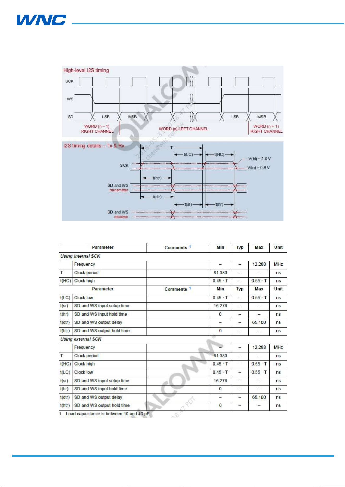
Figure 12. I2S timing diagram
Figure 13. I2S timing parameters
HW
Design
Guidelines
□ Normal □ Internal Use Confidential □ Restricted Confidential
36
/
70
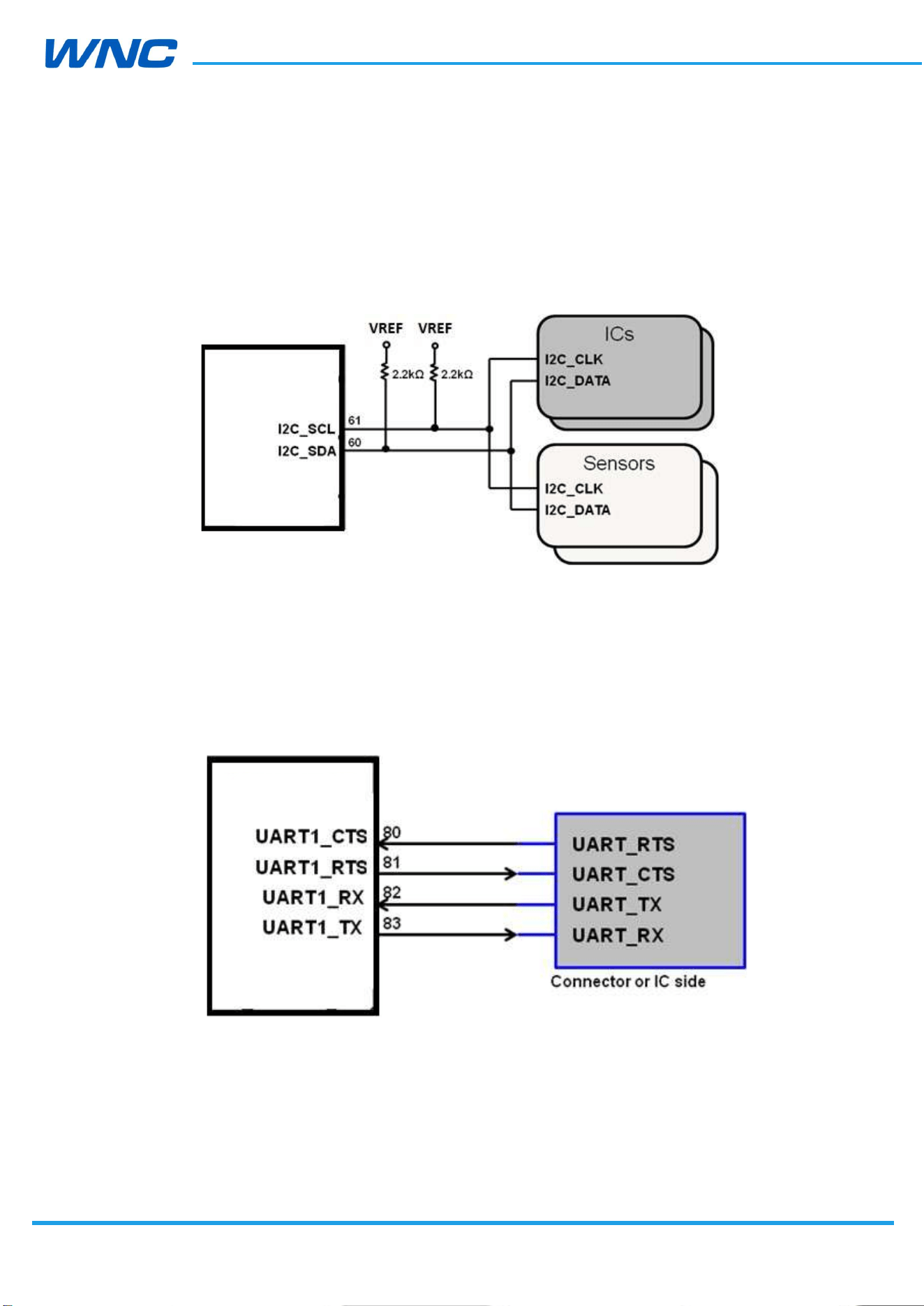
2.7.5. I2C Interface
IMQ8F4 modules provide one I2C interface, I2C only support master mode.
Figure 14. I2C connection (example)
2.7.6. UART Interface
There are two UART interfaces on IMQ8F4: One is a 4 bit UART(UART1) for high-speed data
transfer, max baud rate can be up to 4Mbps. Another is a 2 bit UART(UART2) for diagnostic
tools and debugging, the default baud rate 115200bps is recommended.
Figure 15. UART connection (example)
IMQ8F4
IMQ8F4
HW
Design
Guidelines
□ Normal □ Internal Use Confidential □ Restricted Confidential
37
/
70
2.7.7. ADC Interface
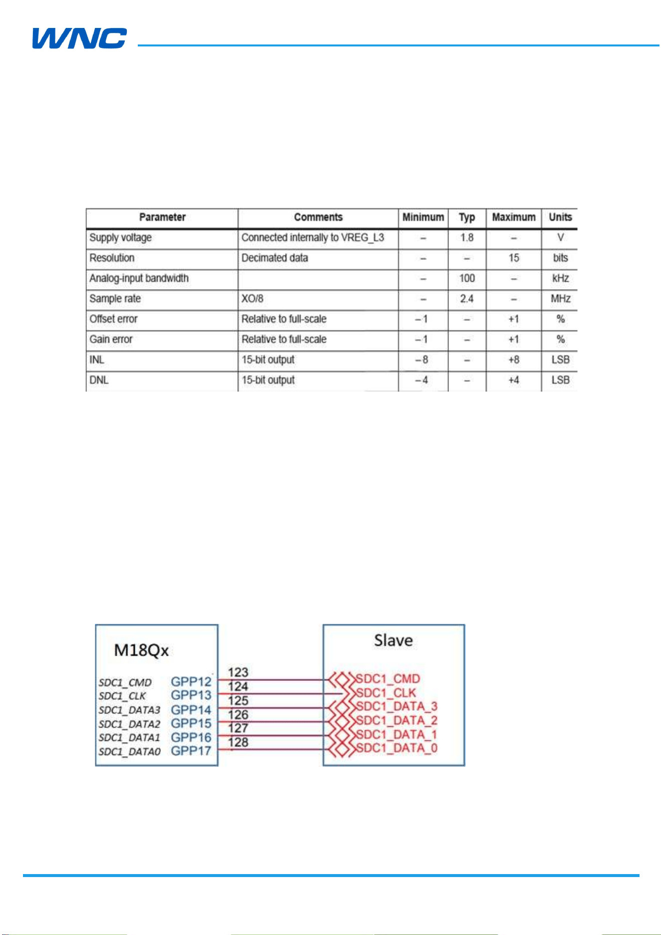
An Analog to Digital Converter (ADC) input is provided by the IMQ8F4. The converter is
16 bit resolution, ranging from 0.1 V to 1.7 V, with a sampling rate of 2.4 MHz.
Figure 16. Analog-to-digital specification
Layout suggestion:
ADC signal trace should be well protected by GND plane
ADC signal trace should be protected from noise and other radiating signals
2.7.8. Secure digital interfaces
IMQ8F4 provides one SDIO interface, muxed with other functionalities, 4-bit 1.8 V for WLAN
interface.
HW
Design
Guidelines
□ Normal □ Internal Use Confidential □ Restricted Confidential
38
/
70
Figure 17. SDIO timing
HW
Design
Guidelines
□ Normal □ Internal Use Confidential □ Restricted Confidential
39
/
70
Pin21
0.5mm
3. RF Specifications
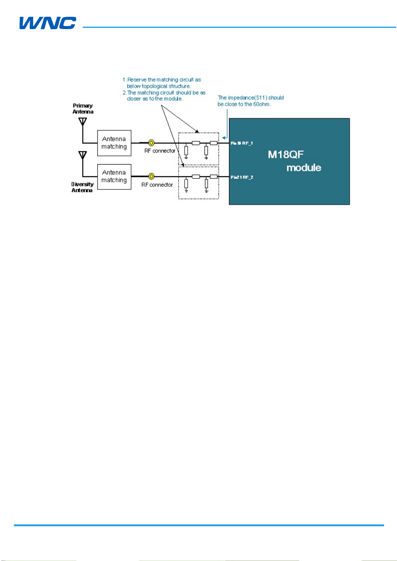
3.1. RF connections
The IMQ8F4 modules have three RF pads; developers must connect them via 50 Ω traces to
the main board.
ANT0_TRX pad (Pin15) – Primary RX/TX path
ANT1_DRX pad (Pin21) – Diversity path
ANT_GNSS pad (Pin9) – GNSS path (For IMQ8F4)
It is recommended that grounds not be present under the surface of the RF pads in the
layout. Details are included below. Layer2 has the same keep out size as Layer1
0.5mm
Pin15
Pin9
Layer1
Layer2
Layer3
GND
GND
Figure 18. RF pad layout suggestion
HW
Design
Guidelines
□ Normal □ Internal Use Confidential □ Restricted Confidential
40
/
70
Figure 19. RF matching guide
3.2. Interference and sensitivity
This section includes tips to assist developers in identifying the interference that may affect
IMQ8F4 modules when used in systems.
Interference from other wireless devices
– Harmonics, inter-modulated signal generated from wireless devices that
fall in RX ranges of the modules, may result in degraded RX performance.
– It is highly recommended to check RX performance of entire systems
within the shielding environment.
Interference from host interface
– High-speed signal-switching elements in systems can easily couple noise
into the module (Ex.: DDR memory, LCD modules, DC-DC converter, PCM
signal).
Methods to avoid sources of interference
– Antenna location is important; we recommend directing the antenna
HW
Design
Guidelines
□ Normal □ Internal Use Confidential □ Restricted Confidential
41
/
70
away from high-speed switching signals. Furthermore, the trace from the
module to the antenna should be as short as possible and must be
shielded by complete grounding.
– The IMQ8F4 modules are well shielded; the high-speed elements
(Ex.: DDR memory, LCD modules, DC-DC converter, PCM signal) on a
system should have shielding reserved during the early stages of
development.
Caution: DDR bus, LCD bus, DC-DC switching and PCM signals are
easily to influence the WWAN and GNSS receiver performance, these
signals must to be routed in the inner layer of the PCB and far away
from the WWAN and GNSS receiver path.
HW
Design
Guidelines
□ Normal □ Internal Use Confidential □ Restricted Confidential
42
/
70
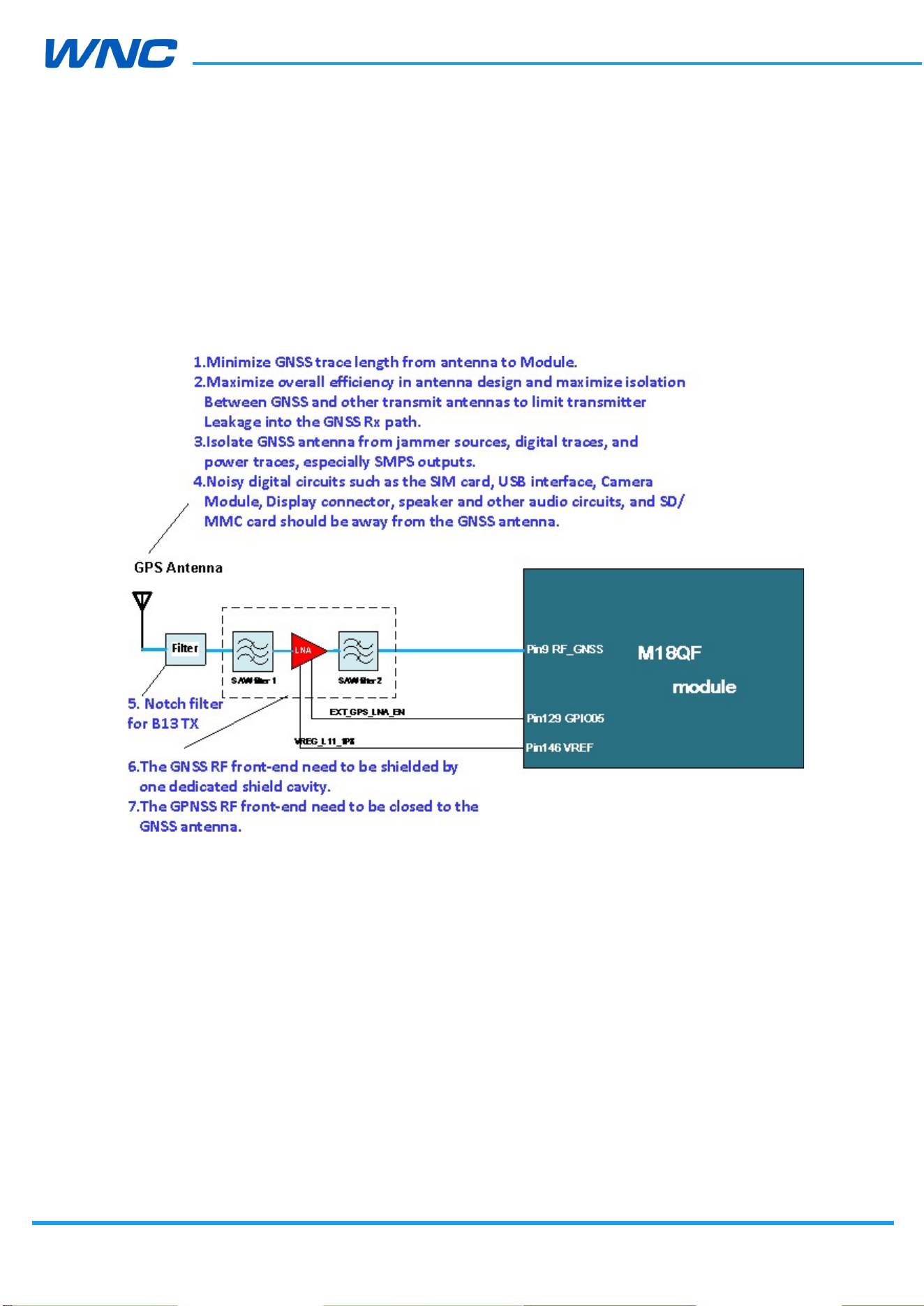
3.3. GNSS external circuit design
One Notch filter, GNSS SAW filter, LNA, and another GNSS SAW filter need to be used
between the module and antenna. Detail design guide as below.
IMQ8F4 module without Band 14
Figure 20. GNSS design suggestion
The following SAW filter and LNA components have been implemented by WNC
development board.
SAW filter1: Murata SAFFB1G56KB0F0AR15
LNA: INFINEON BGA824N6
SAW fiter2: Murata SAFFB1G56KB0F0AR15
If use module embedded GNSS, please follow above reference design. Pin146 (VREF, 1.8V)
of module connects to the external LNA power supply pin. Pin129 (GPIO05) of module
connects to external LNA enable control pin.
HW
Design
Guidelines
□ Normal □ Internal Use Confidential □ Restricted Confidential
43
/
70
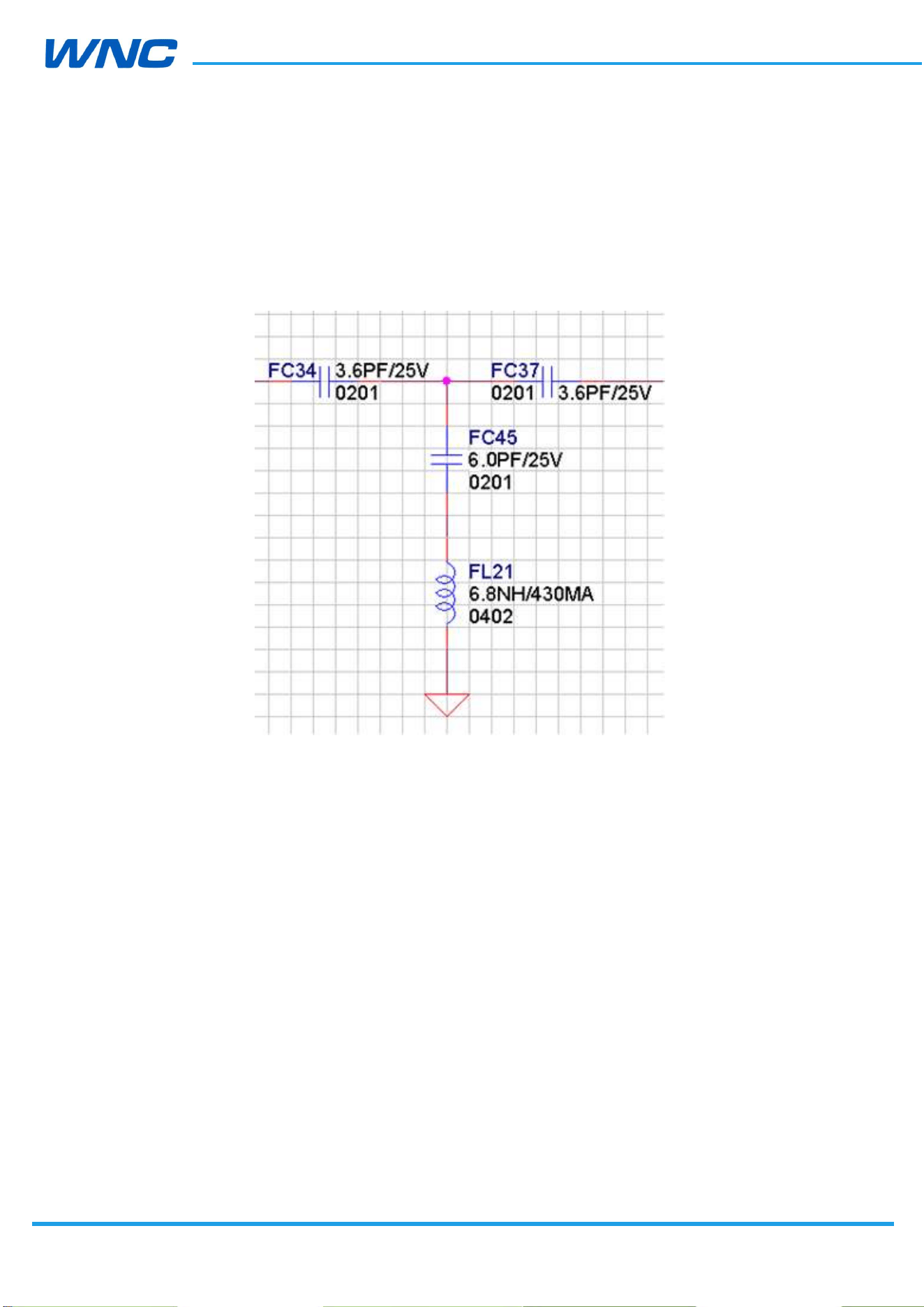
The Notch filter reference design as below:
HW
Design
Guidelines
□ Normal □ Internal Use Confidential □ Restricted Confidential
44
/
70
3.4. RF Specification
3.4.1 Band support
Table 9. Band support
Band Uplink (MHz) Downlink (MHz)
LTE Band 2 1850–1910 1930–1990
LTE Band 4 1710–1755 2110–2155
LTE Band 5 824–849 869–894
LTE Band 12 699–716 729–746
LTE Band 13 777-787 746-756
LTE Band 25 1850-1915 1930-1995
LTE Band 26 814-849 859-894
LTE Band 66 1710-1780 2110-2200
LTE Band 71 663-698 617-652
Band Uplink (MHz) Downlink (MHz)
WCDMA Band 2 1850–1910 1930–1990
WCDMA Band 5 824–849 869–894
HW
Design
Guidelines
□ Normal □ Internal Use Confidential □ Restricted Confidential
45
/
70
3.4.2 Bandwidth support
Table 10. Bandwidth support
Band
Bandwidth
1.4 MHz 3 MHz 5 MHz 10 MHz 15 MHz 20 MHz
LTE Band 2
LTE Band 4
LTE Band 5
- -
LTE Band 12
- -
LTE Band 13 - -
- -
LTE Band 25
LTE Band 26
-
LTE Band 66
LTE Band 71 - -
3.4.3 RF Transmit Specification
Table 11. Conductive Tx output power
Band Items Parameter Unit Min.
Typ.
Max.
LTE Band 2 Max. TX Power 10 MHz 12 RBs/QPSK dBm
20.3 23 25.7
LTE Band 4 Max. TX Power 10 MHz 12 RBs/QPSK dBm
20.3 23 25.7
LTE Band 5 Max. TX Power 10 MHz 12 RBs/QPSK dBm
20.3 23 25.7
LTE Band 12 Max. TX Power 10 MHz 12 RBs/QPSK dBm
20.3 23 25.7
LTE Band 13 Max. TX Power 10 MHz 12 RBs/QPSK dBm
20.3 23 25.7
LTE Band 25 Max. TX Power 10 MHz 12 RBs/QPSK dBm
20.3 23 25.7
LTE Band 26 Max. TX Power 10 MHz 12 RBs/QPSK dBm
20.3 23 25.7
LTE Band 66 Max. TX Power 10 MHz 12 RBs/QPSK dBm
20.3 23 25.7
LTE Band 71 Max. TX Power 10 MHz 12 RBs/QPSK dBm
20.3 23 25.7
Band Items Parameter Unit Min.
Typ.
Max.
WCDMA Band 2
Max. TX power - dBm
20.3
23.5
25.7
WCDMA Band 5
Max. TX power - dBm
20.3 24 25.7
Note: 1.The RF Transmit Specification is defined at the LGA pad.
2. IM8QF4 meet 3GPP TS 36.521-1/TS 34.121-1 test standard.
HW
Design
Guidelines
□ Normal □ Internal Use Confidential □ Restricted Confidential
46
/
70
3.4.4 RF Receiver Specification
Table 12. Conductive Rx sensitivity-3GPP
Band Items Parameter Unit Typ. 3GPP standard
limit
LTE Band 2 RX Sensitivity 10 MHz with 50 RBs dBm
-102.3
–94.3
LTE Band 4 RX Sensitivity 10 MHz with 50 RBs dBm
-102.1
–96.3
LTE Band 5 RX Sensitivity 10 MHz with 50 RBs dBm
-103.3
–94.3
LTE Band 12 RX Sensitivity 10 MHz with 50 RBs dBm
-102.6
–93.3
LTE Band 13 RX Sensitivity 10 MHz with 50 RBs dBm
-102.2
–93.3
LTE Band 25 RX Sensitivity 10 MHz with 50 RBs dBm
-101.9
-92.8
LTE Band 26 RX Sensitivity 10 MHz with 50 RBs dBm
-103.6
-93.8
LTE Band 66 RX Sensitivity 10 MHz with 50 RBs dBm
-102.1
-95.8
LTE Band 71 RX Sensitivity 10 MHz with 50 RBs dBm
-103.2
-93.5
Band Items Parameter Unit Typ. 3GPP standard
limit
WCDMA Band 2
RX Sensitivity dBm
–114 -95
WCDMA Band 5
RX Sensitivity dBm
–114 -95
Note: 1. The RF Receiver Specification is defined at the LGA pad.
2. Meet 3GPP TS 36.521-1/TS 34.121-1 test standard.
Table 13. Conductive Rx sensitivity-CTIA
The below table show the sensitivity data of primary only and second only which is defined
in the CTIA Test Plan for Wireless Device Over-the-Air Performance V 3.4.2 Table 6-6. This
data could be the reference in the OTA performance evaluation.
Band
Channel
Bandwidth
(MHz)
Channel
RX Frequency
(MHz) [center
of DL RB
allocation]
UL RB
Allocati
on
DL RB
Allocation
Primary only
-Typical
(dBm)
Second only
-Typical
(dBm)
2
10
650
1935
50 RB
with
RBstar
t=0
50 RB with
RBstart=0
-99.0
-99.1
50 RB
with
RBstar
t=0
900 1960
50 RB with
RBstart=0
-99.1 -99.2

HW
Design
Guidelines
□ Normal □ Internal Use Confidential □ Restricted Confidential
47
/
70
1150
1985
50 RB
with
RBstar
t=0
50 RB with
RBstart=0
-99.5
-98.8
2000
2115
50 RB
with
RBstar
t=0
50 RB with
RBstart=0
-99.1
-98.9
4
10
2175
2132.5
50 RB
with
RBstar
t=0
50 RB with
RBstart=0
-99.4
-99.3
2350
2150
50 RB
with
RBstar
t=0
50 RB with
RBstart=0
-99.0
-99.1
2450
874
50 RB
with
RBstar
t=0
50 RB with
RBstart=0
-100.4
-100.7
5
10
2525
881.5
50 RB
with
RBstar
t=0
50 RB with
RBstart=0
-100.4
-100.4
2600
889
50 RB
with
RBstar
t=0
50 RB with
RBstart=0
-100.2
-100.3
12
10
5060
734.0
50 RB
with
RBstar
t=0
50 RB with
RBstart=0
-99.5
-100.0
50 RB
with
RBstar
t=0
5095 737.5
25 RB with
RBstart=0
-99.7
-100.2

HW
Design
Guidelines
□ Normal □ Internal Use Confidential □ Restricted Confidential
48
/
70
5130
741.0
50 RB
with
RBstar
t=5
25 RB with
RBstart=0
-99.6
-99.7
13
10
5230
751
50 RB
with
RBstar
t=0
50 RB with
RBstart=0
-99.5
-99.7
8090
1935
50 RB
with
RBstar
t=0
50 RB with
RBstart=0
-99.0
-98.9
25
10
8365
1962.5
50 RB
with
RBstar
t=0
50 RB with
RBstart=0
-99.2
-99.3
8640
1990
50 RB
with
RBstar
t=0
50 RB with
RBstart=0
-99.2
-98.8
8740
864
50 RB
with
RBstar
t=0
50 RB with
RBstart=0
-100.2
-100.4
26
10
8865
876.5
50 RB
with
RBstar
t=0
50 RB with
RBstart=0
-100.6
-100.8
8990
889
50 RB
with
RBstar
t=0
50 RB with
RBstart=0
-100.2
-100.3
66486
2115
50 RB
with
RBstar
t=0
50 RB with
RBstart=0
-99.2
-98.9

HW
Design
Guidelines
□ Normal □ Internal Use Confidential □ Restricted Confidential
49
/
70
66
10
66786
2145
50 RB
with
RBstar
t=0
50 RB with
RBstart=0
-99.3
-99.4
67086
2175
50 RB
with
RBstar
t=0
50 RB with
RBstart=0
-99.4
-98.9
68636
622
50 RB
with
RBstar
t=0
50 RB with
RBstart=0
-100.2
-100.1
71
10
68761
634.5
50 RB
with
RBstar
t=0
50 RB with
RBstart=0
-100.1
-100.5
68886
647
50 RB
with
RBstar
t=0
50 RB with
RBstart=0
100.3
-100.5
Note: 1. The RF typical data is defined at the LGA pad.
HW
Design
Guidelines
□ Normal □ Internal Use Confidential □ Restricted Confidential
50
/
70
3.4.5 GNSS Receiver Specification
Table 14. GNSS receiver performance
Test items Parameter Min.
Typ.
Max.
Cold start TTFF
(@-130dBm)
- 38S -
Hot start TTFF
(@-130dBm)
- 2S -
CEP-50 Accuracy
Open sky with -130 dBm
input
- <3m -
Cold start sensitivity
Acquire First with Signal level
- -146dBm
-
Tracking sensitivity(GPS) Detect an in-view satellite
50% of the time
-158dBm -160dBm
-
Tracking sensitivity (Glonass)
Detect an in-view satellite
50% of the time
-158dBm TBD
-
Note1: The test point shows as below.
HW
Design
Guidelines
□ Normal □ Internal Use Confidential □ Restricted Confidential
51
/
70
4. Power
4.1. Power consumption
This section describes typical power consumption of IMQ8F4 for reference. The current data
is measured with Linux kernel v3.18 in IMQ8F4 that is powered by VCC 3.8V, connected
with LTE emulator. The measured data is subject to IMQ8F4 kernel version upgrade.
Table 15. LTE power consumption
Working Mode
Conditions
Result
min. max.
Airplane mode
Only Module, no other device 1.00mA 1.6mA
LTE standby (DRX=1.28 sec, BW=10MHz)
Band2/ Band4/ Band5/ Band12/ Band13 TBD TBD
LTE Band2 Working mode
Bandwidth 20MHz,TM3–DLRB 100–ULRB 100– IPV4-UDP ,
TX Power=23dbm,Downlink throughput is 145Mbps via
USB interface by Iperf tool
LTE Band4 Working mode
Bandwidth 20MHz,TM3–DLRB 100–ULRB 100–IPV4-UDP ,
TX Power=23dbm,Downlink throughput is 145Mbps via
USB interface by Iperf tool
LTE Band5 Working mode
Bandwidth 10MHz,TM3–DLRB 50–ULRB 50– IPV4-UDP,
TX Power=23dbm,Downlink throughput is 72Mbps via USB
interface by Iperf tool
LTE Band12 Working mode
Bandwidth 10MHz,TM3–DLRB 50–ULRB 50–IPV4-UDP ,
TX Power=23dbm,Downlink throughput is 72Mbps via USB
interface by Iperf tool
LTE Band13 Working mode
Bandwidth 10MHz,TM3–DLRB 50–ULRB 50–IPV4-UDP ,
TX Power=23dbm,Downlink throughput is 72Mbps via USB
interface by Iperf tool
TBD TBD
TBD --
TBD --
TBD --
TBD --
HW
Design
Guidelines
□ Normal □ Internal Use Confidential □ Restricted Confidential
52
/
70
WCDMA standby(DRX=1.28 sec)
Band2 –WCDMA Standby mode, DRX = 1.28 sec TBD --
Band5 –WCDMA Standby mode, DRX = 1.28 sec TBD --
WCDMA Band2 Working mode
HSPA+ downlink 21 Mbps ,TX Power=23dbm TBD --
WCDMA Band5 Working mode
HSPA+ downlink 21 Mbps ,TX Power=23dbm TBD --
Powering on Conditions Result
Peak power consumption
Power consumption peak when the module is powering
up
550mA --
Power off Conditions Result
Power off consumption
Module is powered off 5uA 10uA
Note: 1. USB and GPS are disabled when testing airplane mode and standby mode.

HW
Design
Guidelines
□ Normal □ Internal Use Confidential □ Restricted Confidential
53
/
70
5. Software Interface
5.1. Support tools
The IMQ8F4 modules are compatible with the following support tools:
WNC IMQ8F4 Connection Manager (WNCCM)
5.2. USB interface
The IMQ8F4 modules support 3GPP standard AT commands and proprietary AT commands;
the MAL Manager SDK is also supported for Linux platforms. Refer to [WNC IMQ8F4/M18QA
Series] WNC MAL Manager Developer Guide for more information.
HW
Design
Guidelines
□ Normal □ Internal Use Confidential □ Restricted Confidential
54
/
70
6. Mechanical and Environmental
Certifications
6.1. PCBA Form Factor
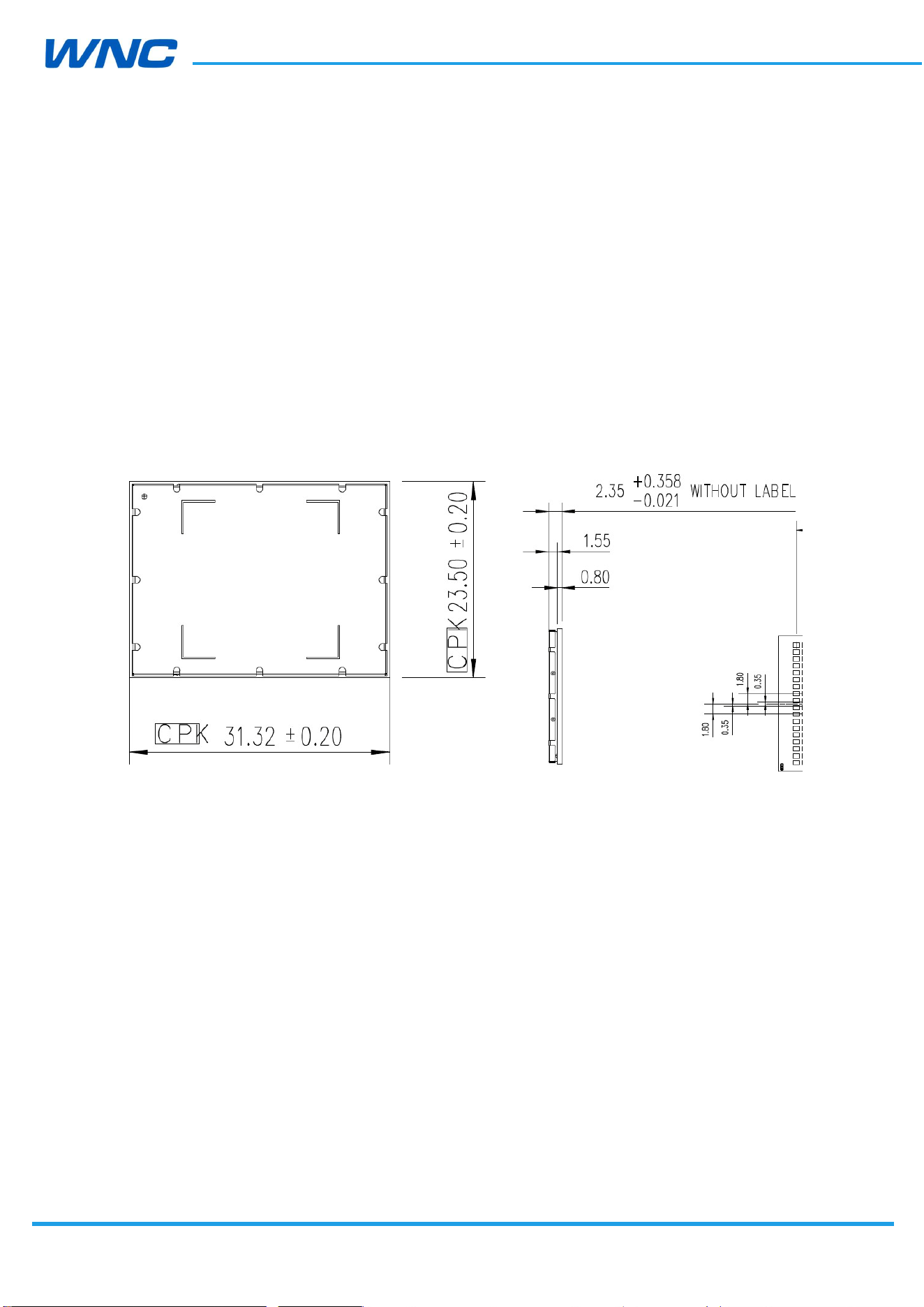
IMQ8F4 modules have the same dimensions:
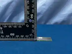
31.32 mm (typ.) × 23.5 mm (typ.) × 2.35 mm (typ.)
Top
view
Right
view
Figure 21. PCBA dimension
HW
Design
Guidelines
□ Normal □ Internal Use Confidential □ Restricted Confidential
55
/
70
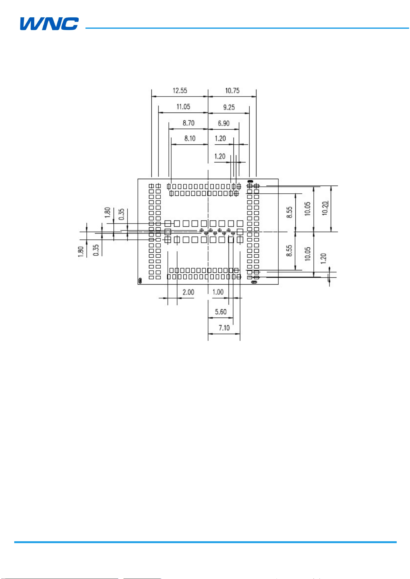
Figure 22. Pad dimension(Bottom view)
HW
Design
Guidelines
□ Normal □ Internal Use Confidential □ Restricted Confidential
56
/
70
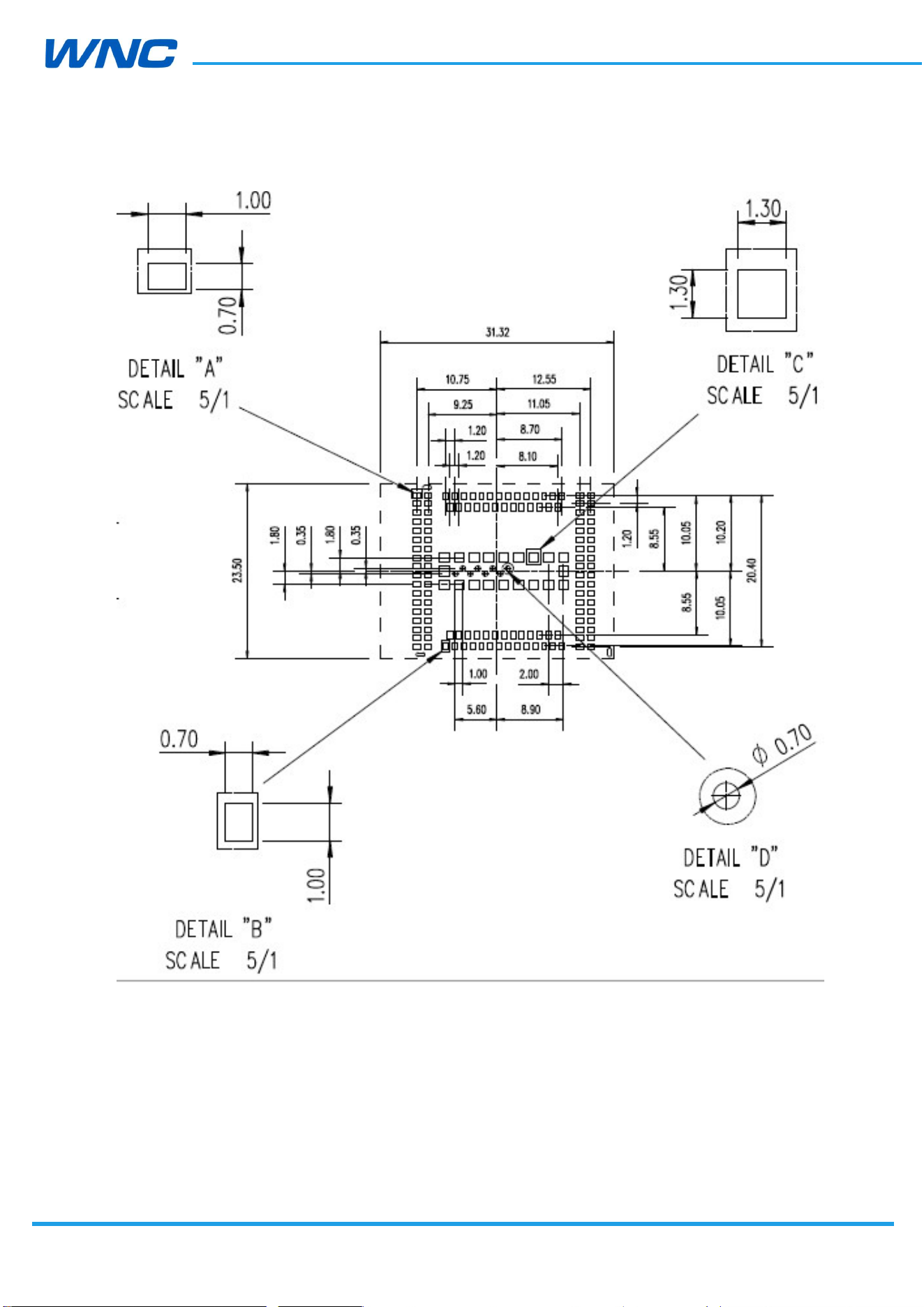
Figure 23. PCB footprint suggestion
HW
Design
Guidelines
□ Normal □ Internal Use Confidential □ Restricted Confidential
57
/
70
6.2. Module orientation
Pin1
Location
HW
Design
Guidelines
□ Normal □ Internal Use Confidential □ Restricted Confidential
58
/
70
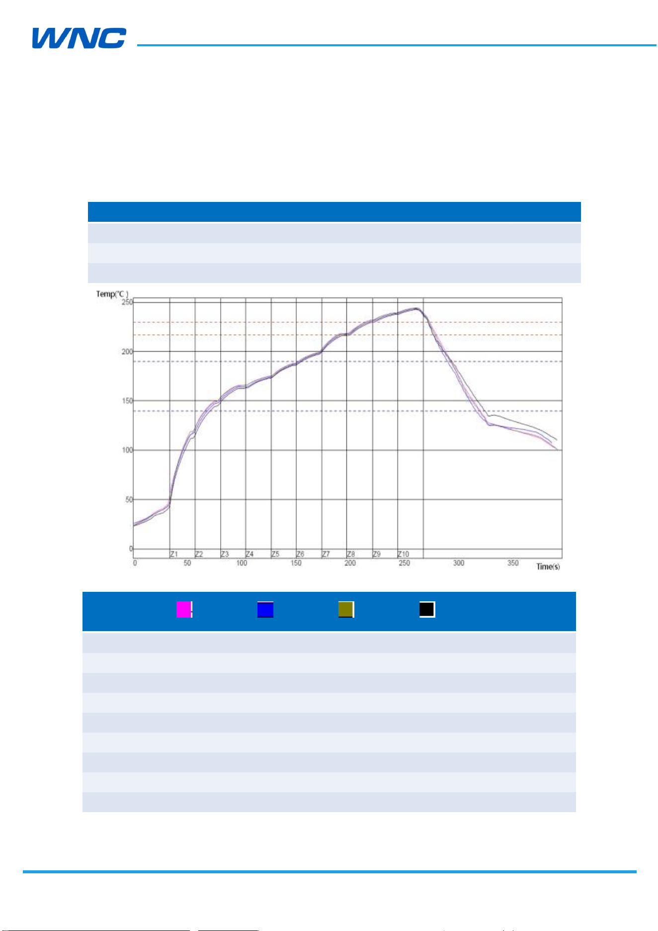
6.3. Reflow
This section details the recommended reflow profile when the module is mounted onto
other boards.
Temp. Region 1 2 3 4 5 6 7 8 9 10
Upper temp. region 150
165
175
180
195
205
230
235
250
245
Lower temp. region 150
165
175
180
195
205
230
235
250
245
Conveyer band speed
95 cm/minute
PWI = 91%
D31-1
D31-2 D31-3 D31-4
Temp.
Difference
Preheat from 140–190°C
85.34 85.30 86.06 84.29 1.77
–12% –13% –8% –18%
Melt-out Time/230°C
59.07 55.03 58.70 49.70 9.37
91% 50% 87% –3%
Max Temp
244.27 243.56 244.33 242.71 1.62
43% 36% 43% 27%
HW
Design
Guidelines
□ Normal □ Internal Use Confidential □ Restricted Confidential
59
/
70
Total Time/217°C
90.55 85.88 90.09 76.90 13.65
22% 4% 20% –32%
Gradient1 (100–150°C)
1.91 1.83 1.93 1.78 0.15
27% 22% 29% 19%
Process limit:
Solder Paste
Lead-free
Profile feature Min. Max. Unit
Gradient1 (Target = 1.5) (100 °C–150 °C)
(Time period = 20 s)
0 3 °C/S
Preheat time from 140 °C to 190 °C 70 105 S
Time maintained above 230 °C 40 60 S
Peak package body temperature 230 250 °C
Time maintained above 217 °C 60 110 S
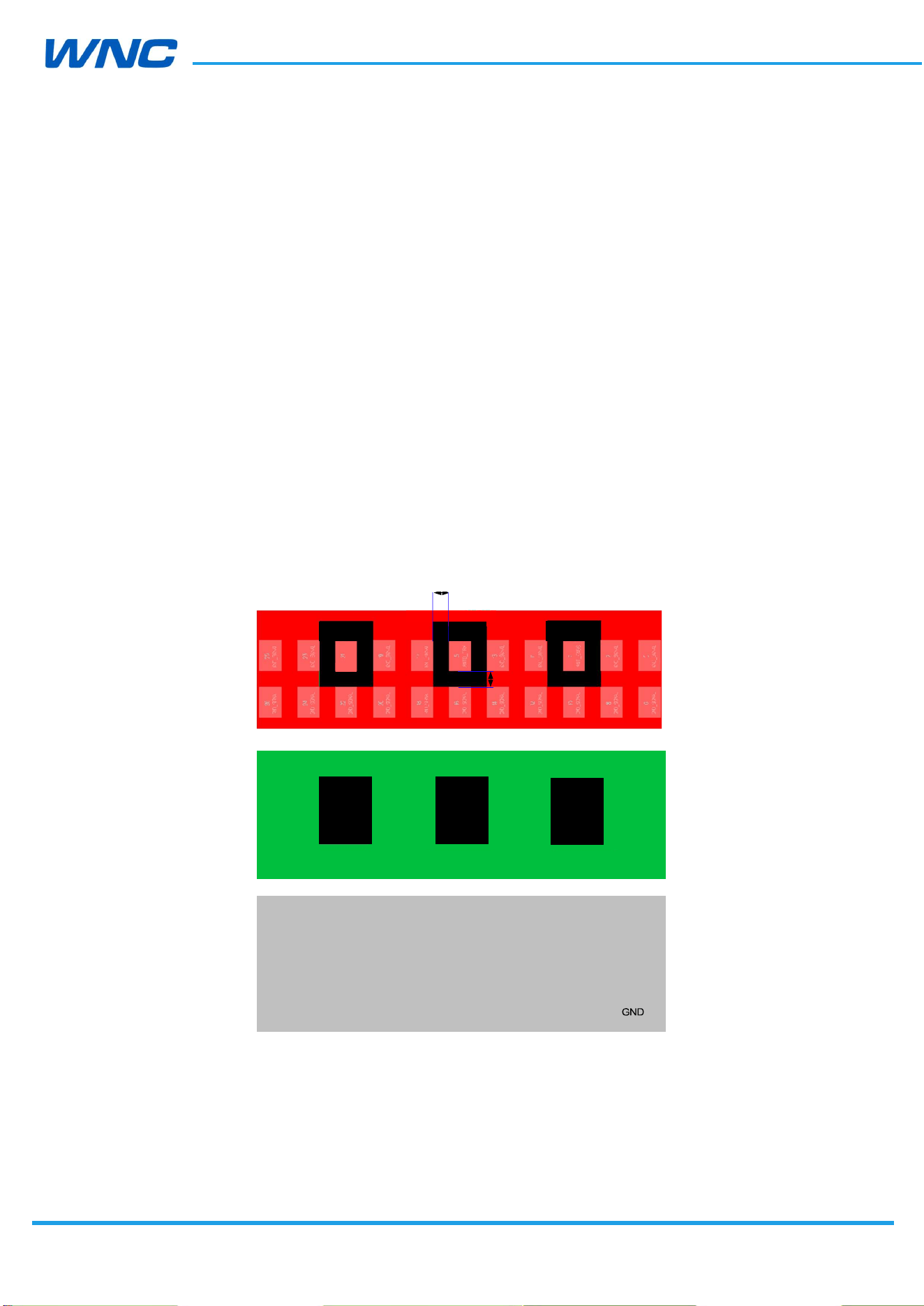
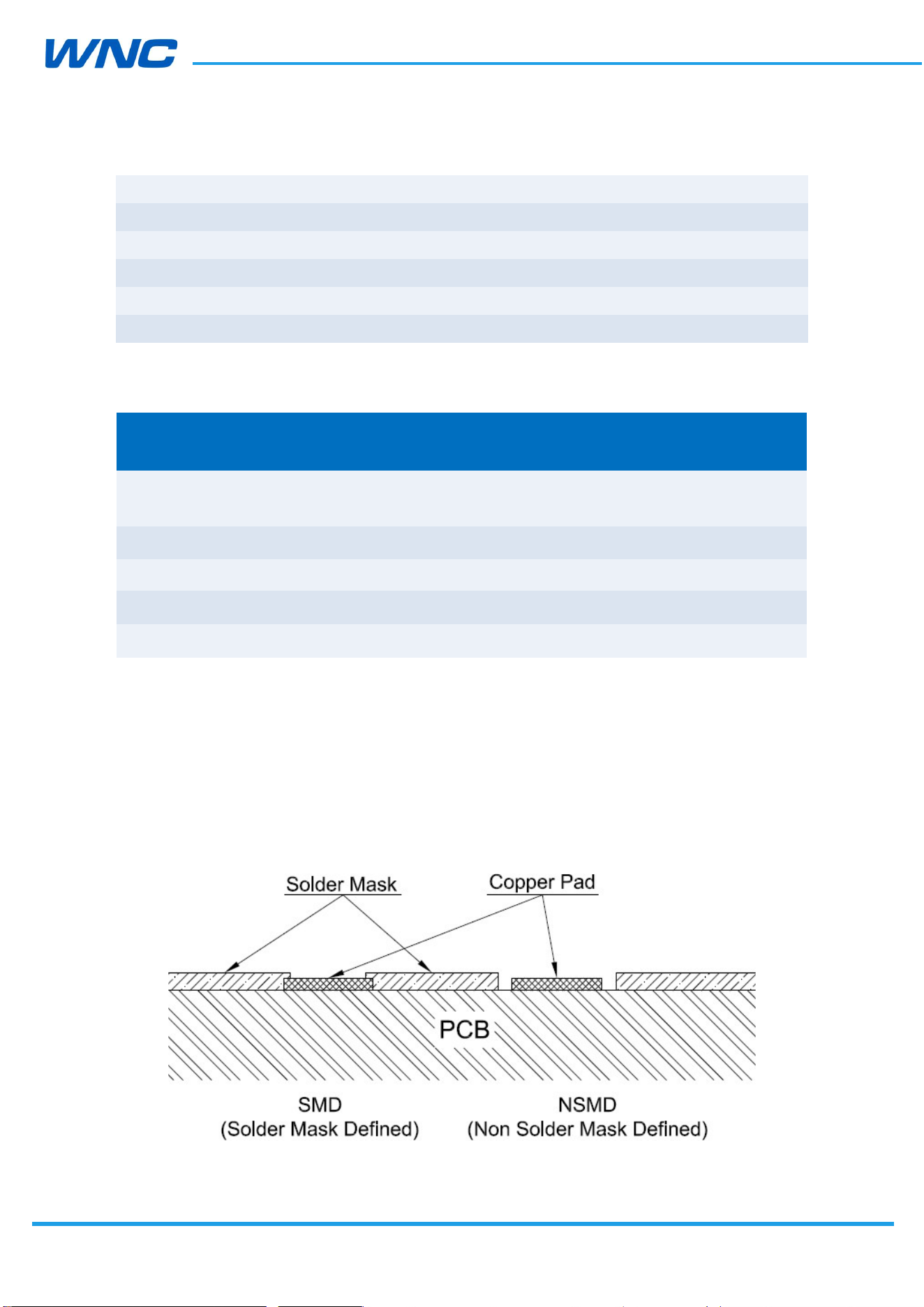
6.4. PCB pad design
Non solder mask defined (NSMD) type is recommended for the solder pads of the PCB on
which IMQ8F4 Series modules will be mounted, this kind of design is good to soldering
reliability in SMT process.
Figure 24. NSMD solder pad design
HW
Design
Guidelines
□ Normal □ Internal Use Confidential □ Restricted Confidential
60
/
70
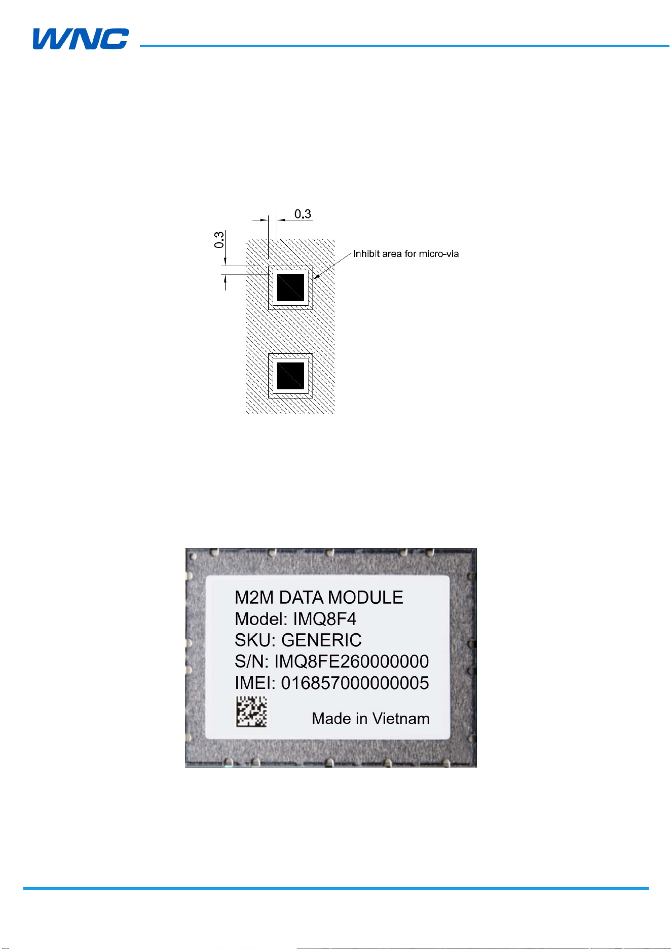
It is not recommended to place via or micro-via not covered by solder resist in an area of
0.3 mm around the pads unless it carries the same signal of the pad itself, see following
figure.
Holes in pad are allowed only for blind holes and not for through holes.
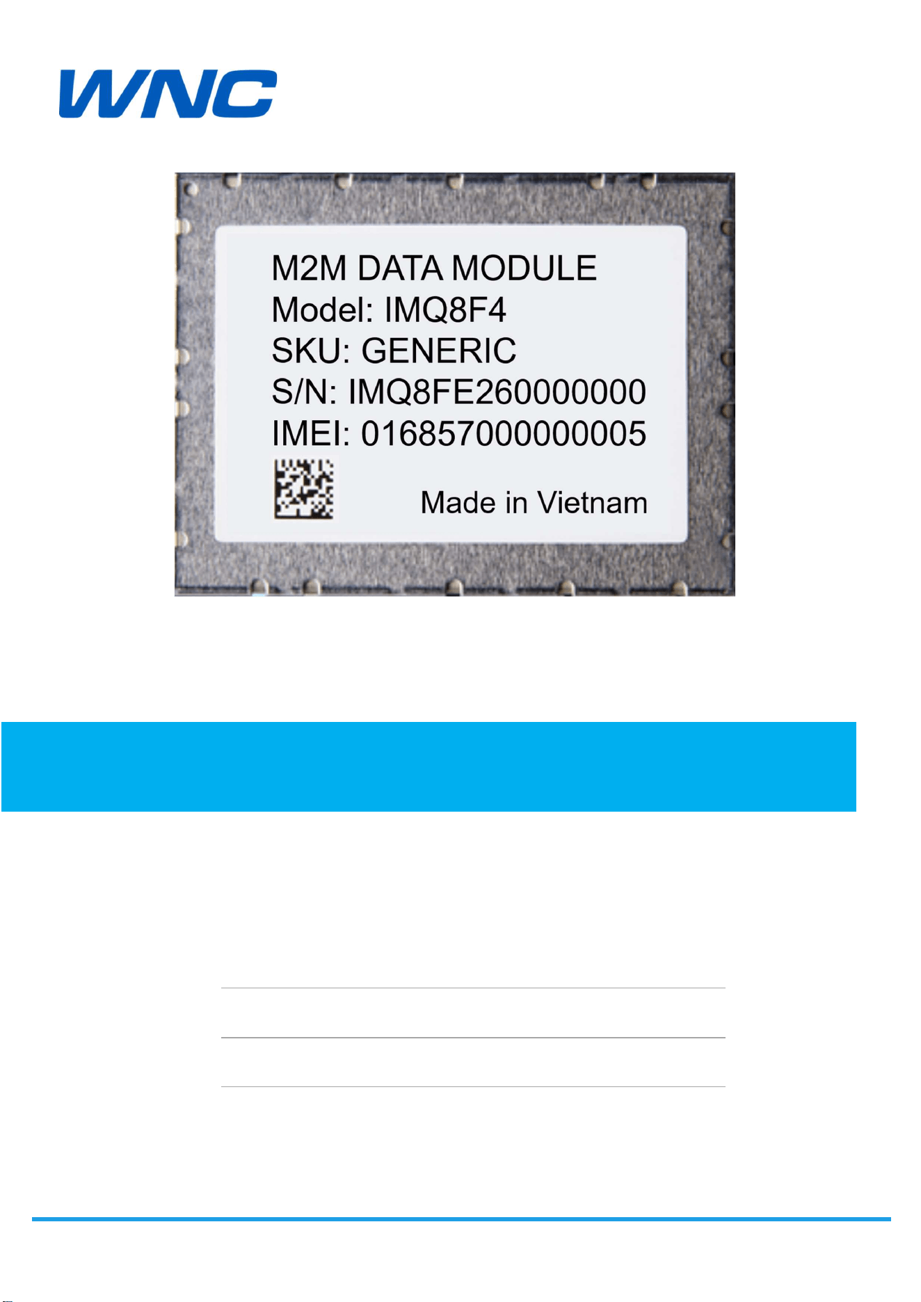
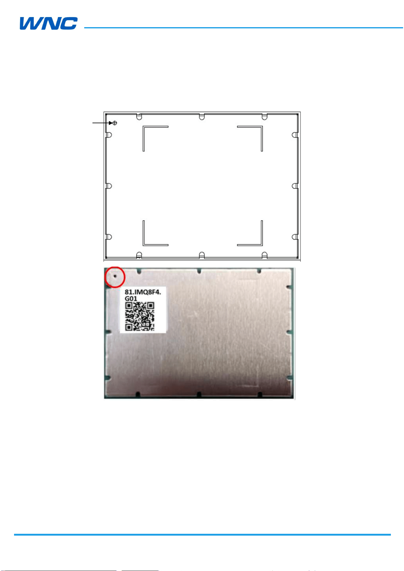
6.5. Labeling
Figure26 shows label drawing of IMQ8F4 modules.
Figure 25. Label drawing
HW
Design
Guidelines
□ Normal □ Internal Use Confidential □ Restricted Confidential
61
/
70
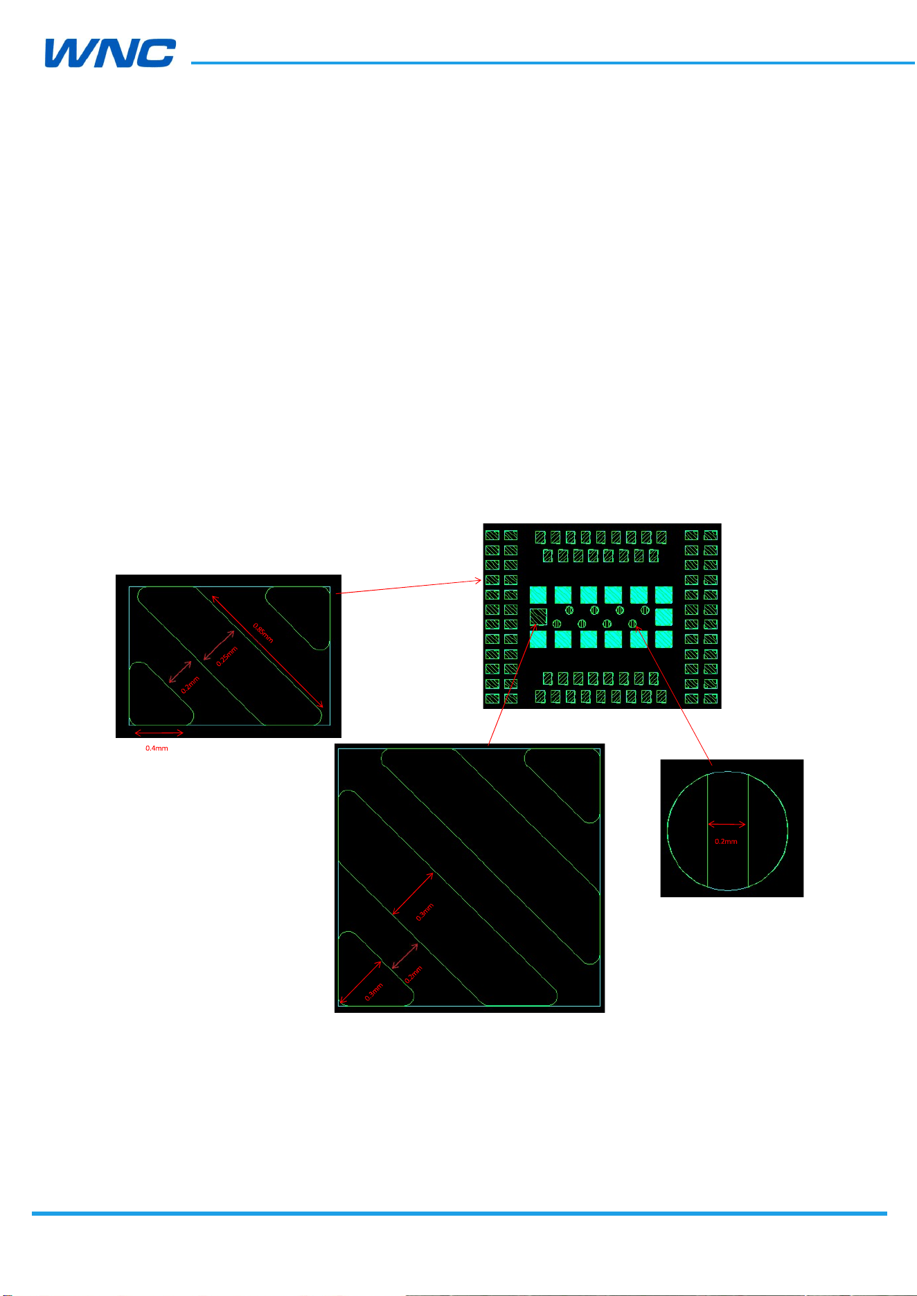
6.6. SMT Voids control
6.6.1. Mother board PCB thickness
Thin mother board is prone to warping during SMT reflow, which creates voids when the
module is soldered. Therefore, the thickness of the mother board needs to be larger than 1.2
mm, and the larger the size of the mother board, the larger the thickness. For example,
1.4mm, 1.6mm.
6.6.2. Stencil design
The thickness of the stencil is at least 0.15 mm, and the thickness of the stencil need to be
increased depending on the actual situation. For example, there is open soldering still.
Figure 26. Stencil-foil drawing

HW
Design
Guidelines
□ Normal □ Internal Use Confidential □ Restricted Confidential
62
/
70
6.7. Thermal considerations
Grade
Operatin
g 3GPP
compl
iant Functional
work Storage
Industrial –40 °C~+8
5
°C –20
°C~+60
°C –40
°C~+8
5 °C –40 °C ~+85 °C
Note: The temperature above refers to ambient temperature.
The case temperature of module shielding cover must be < 85 °C when integrated to
prevent damage.
Design points used to improve the thermal performance:
It’s better to add a naked copper area onto IMQ8F4 modules’ back side of the
PCB. If the thermal performance becomes an issue in the customer’s product,
add thermal solutions for improvement such as a thermal pad or a heat sink.
It’s recommended to have a thermal pad or a heat sink on shielding cover to
help transfer heat.
If systems with IMQ8F4 modules embedded intend to work under ambient
temperatures as low as -40°C, it’s suggested that:
1. SIM Card need to be well arranged to make sure it is functional at the
condition of ambient temperature as low as -40°C.
2. Adding heating circuit on board design, the circuit mainly consists of
temperature sensing unit, heating element and control unit.

HW
Design
Guidelines
□ Normal □ Internal Use Confidential □ Restricted Confidential
63
/
70
7. Regulatory Compliance and Certification
7.1. Certification testing
PTCRB, GCF, FCC, IC, AT&T TA and Verizon TA
HW
Design
Guidelines
□ Normal □ Internal Use Confidential □ Restricted Confidential
64
/
70
8. Packaging
8.1. Tape-and-Reel Package
The IMQ8F4 modules are delivered in tape and reel.
Figure 27. Packing--tape
HW
Design
Guidelines
□ Normal □ Internal Use Confidential □ Restricted Confidential
65
/
70
Figure 28. Packing—reel
Figure 29. Packing—carton
HW
Design
Guidelines
□ Normal □ Internal Use Confidential □ Restricted Confidential
66
/
70
8.2. Single Packaging for Samples
Samples are packaged at 50 pcs. /box. There is no vacuum packaging. Samples must be
baked for 8 hours at least at 85 °C before SMT.
8.3. MSL level
The module MSL level is 3.

HW
Design
Guidelines
□ Normal □ Internal Use Confidential □ Restricted Confidential
67
/
70
9. Safety Recommendation
Be sure the use of this product is allowed in the country and in the environment required.
The use of this product may be dangerous and must be avoided in the following areas:
Where it can interfere with other electronic devices in environments such as
hospitals, airports, and aircraft
Where there is a risk of explosion such as gasoline stations and oil refineries
It is the responsibility of the user to comply with his or her country’s regulations and the
specific environmental regulations.
Do not disassemble the product; any mark of tampering will compromise the warranty’s
validity.
We recommend following the instructions of the hardware user guides for a correct wiring
of the product. The product must be supplied with a stabilized voltage source, and the
wiring must conform to the security and fire-prevention regulations.
This product must be handled with care; avoid any contact with the pins because
electrostatic discharge may damage the product. Same caution must be taken regarding the
UIM card; carefully check the instructions for its use. Do not insert or remove the UIM when
the product is in power-saving mode.
The system integrator is responsible of the functioning of the final product; therefore, care
must be taken for the external components of the module as well as for project or
installation issues—there may be a risk of disturbing the GSM network or external devices
or of having an impact on device security. If you have any doubts, please refer to the
technical documentation and the relevant regulations in force.
Every module must be equipped with a proper antenna with specific characteristics. The
antenna must be installed with care in order to avoid any interference with other electronic
devices.

HW
Design
Guidelines
□ Normal □ Internal Use Confidential □ Restricted Confidential
68
/
70
10. Warning
FEDERAL COMMUNICATIONS COMMISSION INTERFERENCE STATEMENT
This equipment has been tested and found to comply with the limits for a Class B digital
device, pursuant to part 15 of the FCC Rules. These limits are designed to provide
reasonable protection against harmful interference in a residential installation. This
equipment generates, uses and can radiate radio frequency energy and, if not installed and
used in accordance with the instructions, may cause harmful interference to radio
communications. However, there is no guarantee that interference will not occur in a
particular installation. If this equipment does cause harmful interference to radio or
television reception, which can be determined by turning the equipment off and on, the
user is encouraged to try to correct the interference by one or more of the following
measures:
-Reorient or relocate the receiving antenna.
-Increase the separation between the equipment and receiver.
-Connect the equipment into an outlet on a circuit different from that to which the
receiver is connected.
-Consult the dealer or an experienced radio/ TV technician for help.
CAUTION:
Any changes or modifications not expressly approved by the grantee of this device could
void the user's authority to operate the equipment.
This device complies with Part 15 of the FCC Rules. Operation is subject to the following
two conditions: (1) this device may not cause harmful interference, and (2) this device
must accept any interference received, including interference that may cause undesired
operation.
This module is intended for OEM integrator. The OEM integrator is responsible for the
compliance to all the rules that apply to the product into which this certified RF module is
integrated. Additional testing and certification may be necessary when multiple modules
are used.

HW
Design
Guidelines
□ Normal □ Internal Use Confidential □ Restricted Confidential
69
/
70
USERS MANUAL OF THE END PRODUCT:
In the user’s manual of the end product, the end user has to be informed to keep at least
20cm separation with the antenna while this end product is installed and operated.
The end user has to be informed that the FCC radio-frequency exposure guidelines for an
uncontrolled environment can be satisfied.
The end user has to also be informed that any changes or modifications not expressly
approved by the manufacturer could void the user's authority to operate this equipment.
Operation is subject to the following two conditions: (1) this device may not cause harmful
interference and (2) this device must accept any interference received, including
interference that may cause undesired operation.
LABEL OF THE END PRODUCT:
The final end product must be labeled in a visible area with the following " Contains TX FCC
ID: NKRIMQ8F4 ".
RF Exposure warning
This equipment must be installed and operated in accordance with provided instructions
and the antenna(s) used for this transmitter must be installed to provide a separation
distance of at least 20 cm from all persons and must not be co-located or operating in
conjunction with any other antenna or transmitter. End-users and installers must be
provide with antenna installation instructions and transmitter operating conditions for
satisfying RF exposure compliance.

HW
Design
Guidelines
□ Normal □ Internal Use Confidential □ Restricted Confidential
70
/
70
Canada, Industry Canada (IC) Notices
This device contains licence-exempt transmitter(s)/receiver(s) that comply
with Innovation, Science and Economic Development Canada’s licence-exempt RSS(s).
Operation is subject to the following two conditions:
1. This device may not cause interference.
2. This device must accept any interference, including interference that may cause
undesired operation of the device.
Canada, avis d'Industry Canada (IC)
Cet appareil contient un ou des émetteurs/récepteurs exempts de licence conformes aux
RSS exempts de licence d'Innovation, Sciences et Développement économique Canada. Le
fonctionnement est soumis aux deux conditions suivantes:
1. Cet appareil ne doit pas causer d'interférences.
2. Cet appareil doit accepter toutes les interférences, y compris les interférences pouvant
entraîner un fonctionnement indésirable de l'appareil.
Radio Frequency (RF) Exposure Information
The radiated output power of the Wireless Device is below the Innovation, Science and
Economic Development Canada (ISED) radio frequency exposure limits. The Wireless
Device should be used in such a manner such that the potential for human contact during
normal operation is minimized.
This device has also been evaluated and shown compliant with the IC RF Exposure limits
under mobile exposure conditions. (Antennas are greater than 20cm from a person's
body).
Informations concernant l'exposition aux fréquences radio (RF)
La puissance de sortie rayonnée de l'appareil sans fil est inférieure aux limites d'exposition
aux radiofréquences d'Innovation, Sciences et Développement économique Canada (ISDE).
L'Appareil sans fil doit être utilisé de telle manière que le potentiel de contact humain
pendant le fonctionnement normal soit minimisé.
Cet appareil a également été évalué et démontré conforme aux limites d'exposition RF IC
dans des conditions d'exposition mobile. (Les antennes sont à plus de 20 cm du corps
d'une personne).