
~4ch
BVANTESIZED
STARE
TUNER
BT
EEReSRouR
ERE
Ze
ee
ee
eS
ee
ES
See
Ee
a
fe
pee
2
eae
ee
Se
ee
eee
Pee
i
Se
fe
A
ee
oe
eee
Se
oe
Be
Be
R

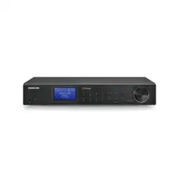
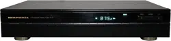
MODEL
ST-40/ST-40L
TECHNICAL
SPECIFICATIONS
(DIN)
FM
Stage
87.5~108
MHz
Sensitivity
DINIMmOnNG
(S/n
26:08
75
ONMS)iou
sia
eee
ey
eee
hohe
eeu
aeeitade
Cateye
StL
iee
ite
eee
eee
0.9
pV
DIN:Stereo(S/n-46
dB
75
ONIMNS)\na5.o
6
renee
ete
eee
ee
eels
eae
ehh
Lowe
eee
ee
eet
a
25
uv
Selectivity
acqjacent
Channel:98-
WAZ
.ks
sve
oa
wa
aod
ee
Ge
eae
eae
e
ee
Aha
ee
SA
65
dB
Tuner
OUIDUL.C
Khiz-75:.
KZ
Deviation)
2s.
a8
ow
So's
wei
ecete
data
eee
OS
a
eed
Saree
@
Gate
eee
whe
ees
940
mV
Signal
to
noise
ratio
o/
NC
DIN
WEIQNIEG
ANOMO:
wae
ox3e
ee
Reeok
SAS
eked
sae
a
eee
hoe
FERRE
RS
eae
ae
ae
eats
80
dB
S/NUDIN
WeldileG:Stereo
4.5.
wie
wnat
addwwed
teehee
Pe
ee
edad
eae
ee
od
ine
Ee
a
ees
73
dB
Olah
NarmnGniG:
CIStOmlOn
MONO:
>
24a.
tnd.
Gated
oes
ee
See
aes
agar
et
Rates
OP
a
eS
et
IL
0.1%
VOtal
HAnnOnie-GIStOmiOn-
SICKO:
vf
6-454
bss
6
Seeds
ese
ciece
bya
dete
aes
aie
A
Ee
Oe
eee
See
Sa
0.2%
Accuracy
of
frequency
response
ACTOSS
OU
id
Tou
izZ-
DanGWIGUn
22h
scp
ciscw
hw
ate
Slanted
eho
at
evan
a
ab
wea
ae
Gone
Soe
Oe
Gee
es
+0.5/—2.0
dB
DICLEO
SCD
ANON
spatiaAhaw.
4
purer
esd
2's
Suck
waht
aed
LS
ore
OAD
AT
Ae
es
Se
ee
Ra
eee
ore
aes
45
dB
MW
Stage
(531~1602
kHz)
Sensitivity
(s/y-20
GB
300
mods
1
MAZ)ii03-c0c
ete
Nainvead
aa
ete
eos
Setsa
see
eae
eee
aM
400
pV
SeleCtIVINV
LAWIZ
ORMZ..G
itn
ew
ha
eula
teeta
ene
ee
hre
tees
alt
an
a
a
ea
te
else
we
a.clreutaon
Sites
30
dB
SIGhal
1tOnOiSse
raviOrats
MAZ
te
a
He
es
hee
ponents
a
deh
Sabah
pale
etek
Aa
atte
Saka
Ramee
S
52
dB
LW
Stage
(152~282
kHz)
SENSItIVITV-(S/
mM.
20GB
3070
IMOd:
co
KHZ).25
osc
adepsede
le
eg
oreo
ar
Pesan
See
ek
antes
800
pV
Signal
10:
No@lse
(alle
al
250
KAZ:
Mins
onde
acetone
obs
ee
eae
Onesie
clear
Me
he
bk
ewaticases
....
00
dB
General
Power
Requirements
(02
ANG
(50,
OO
VEISIONS
2k.
bs
ond
eord
boi
ek
Brnhaes
e
hee
SaaS
ea
hee
eee
ete
yee
220/240V
AC,
50/60
Hz
FOU
NOPSIORNN
GN
ONAOGS)).
cnet
or
taostd
anid
dard
dee
aay
Gry
anasg
ME
Ce
Bee
Baye
ed
ee
110/120/220/240V
AC,
50/60
Hz
Dimensions
FRAG
VVIOLO)
sed
Arcect
sti
aba
te
Cue
ors,
Bua
atone
ar
a
es
cesar
a
at
Nine
hae
sia,
o
ane
cele
a
ee
ea
er
i
420
mm
PAM
i
ClO
Mss,
5th
pea
ul
a
Be
Peace
ar
ew
te
Esai
wae
ured
trae
Gh
ese
CON
Sees
aah
Be ae
A
Ol
a
aan
ode
Ga
eG
ne
Joep
73mm
PISO
4.
ek
ees
ated
Bakes
erecta
eh
a
th
ae
ge AS
Sacer
Big
Ae
de
a
dw
bo
ted
arena
aod
ooh
ane
Sanaa
Queecatodar
ath
Syke
ts
280
mm
Weight
Ia
ORIG
eats
oe
ae
or
eset
oe
ua
Bie
cess
wo
nea
ripe
Wen
A
See
ae
eee
de
ee
ee
Ne
Rees
BS
ake
eee
ie
3.3
kg
Specifications
subject
to
change
without
prior
notice.
MZ
2574

MARANTZ
DESIGN
AND
SERVICE
Using
superior
design
and
selected
high
grade
|
components,
MARANTZ
company
has
created
the
ultimate
in
stereo
sound.
Only
original
MARANTZ
parts
can
insure
that
your
MARANTZ
product
will
continue
to
perform
to
the
specifications
for
which
it
is
famous.
Parts
for
your
MARANTZ
equipment
are
generally
MARANTZ
INTERNATIONAL
Vestdijk
9
5600
MD_
Eindhoven
The
Netherlands
Phone:
+31/40.758290
Telefax:
+31/40.75.82.99
available
to
our
National
Marantz
Subsidiary
or
Agent.
ORDERING
PARTS:
Parts
can
be
ordered
either
by
mail
or
by
telex.
In
both
cases,
correct
part
number
has
to
be
specified.
The
following
information
must
be
supplied
to
eliminate
delays
in
processing
your
order:
1.
Complete
address
.
Way
of
shipment
oO
or
&
GNM
.
Complete
part
numbers
and
quantities
required
.
Description
of
parts
.
Model
number
for
which
part
is
required
.
Signature:
any
order
form
or
telex
must
be
signed
otherwise
such
part
order
will
be
considered
as
null
and
void.
PARTS
ORDERING
Parts
may
be
ordered
at
the
following
addresses:
AUSTRIA
HORNYPHON
Vertriebsgesellschaft
GmbH
Wienerbergstrasse
1
A
1101
Wien
Austria
Telex:
132.332
BELGIUM
SVD
DIVISION
MARANTZ
Industrialaan
14
1720
Groot-Bijgaarden
Belgium
Telex:
24466
CHILE
MARANTZ
DIVISION
OF
PHILIPS
S.A.
AV.
Santa
Maria,
0760
Casilla
2687
Santiago
Telex:
240.239
DENMARK
MARANTZ
DIVISION
OF
PHILIPS
SERVICE
A/S
Prags
Boulevard
80
Postbox
1919
DK-2300
Kgbenhavn
S
Denmark
Telex:
31201
FINLAND
MARANTZ
DIVISION
OF
OY
PHILIPS
Ab
Kaivokatu
8
00100
Helsinki
Finland
Telex:
124811
FRANCE
MARANTZ
FRANCE
4
Rue
Bernard
Palissy
92600
Asniéres
France
Telex:
611651
GERMANY
MARANTZ
GERMANY
GmbH
Alexanderstrasse
1
2000
Hamburg
Germany
THE
NETHERLANDS
Elpro
Marantz
Wint
Hontlaan
28
3526
KV
Utrecht
The
Netherlands
Telex:
4748
NORWAY
MARANTZ
DIVISION
OF
PHILIPS
A/S
Sandstuveien
40
0680
Oslo
6
Norway
Telex:
72640
GREAT
BRITAIN
MARANTZ
AUDIO
U.K.
Ltd
Unit
15/16
Saxon
Way
Industrial
Estate
Moor
Lane
Harmondsworth
UB7
OLW
Great
Britain
Telex:
935196
GREECE
SHERTON
ELECTRONICS
S.A.
P.O.Box
21025
Hippocratus
Street
188
Athens
11471
Greece
Telex:
216.795
JAPAN
MARANTZ
JAPAN,
Inc.
35-1,
7-chome,
Sagamiono
Sagamihara-shi,
Kanagawa
Japan
KUWAIT
AL
ALAMIAH
ELECTRONICS
Ussama
Building
Fahd
al
Saleem
Street
P.O.Box
23781
Safat-Kuwait
Telex:
22694
ITALY
MARANTZ
ITALIANA
S.P.A.
Via
Chiese,
74
20126
Milano
Italy
SAUD!
ARABIA
AL
ALAMIAH
ELECTRONICS
P.O.Box
5954
University
Street
Riyadh
11432
Saudi
Arabia
Telex:
401530
SOUTH
AFRICA
MARANTZ
DIVISION
OF
PHILIPS
S.A.
Main
Road
Martindale
P.O.
Box.
58088
Newville
21114
South
Africa
SPAIN
PHONO
S.A.
Ignacio
Iglesias
10
Badalona
(Barcelona)
Spain
Telex:
59355
SWEDEN
MARANTZ
DIVISION
OF
PHILIPS
Forsaljning
AB
Tegeluddsvagen
1
S-115
84
Stockholm
Sweden
Telex:
14060
Telex:
35000
PHTC
NL
routing
IND
NLMTFAT
SWITZERLAND
MARANTZ
Technischer
Service
Duenstrasse
3
3186
Dudingen
Switzerland
TURKEY
DOGRUOL
Ltd.
1.M.C.
6
Blok
N°6310
Unkapani
Istanbul
Turkey
Telex:
22085
MALTA
CACHIA
&
GALEA
Republic
Street,
68D
Valetta
Telex:
1682
PORTUGAL
MARANTZ
Divisao
philips
S.A.
service
Outurela-carnaxide
2795
LinDA-A-VELHA
Telex:
43906
All
of
the
above
locations
are
fully
equipped
to
take
care
of
your
total
service
needs.
Because
various
countries
have
differing
configuration
requirements,
it
is
necessary
that
you
contact
the
service
facility
in
your
particular
country.
In
the
event
that
there
is
no
service
location
listed
for
your
country,
please,
contact
the
nearest
facility
for
the
necessary
In
case
of
difficulties,
do
not
hesitate
to
contact
the
Technical
Department
at
abovementioned
address.
assistance.
MZ
2573

1.
BLOCK
DIAGRAM
G~ed
él
sna
viva
ad
HOLIMS
|
ae
|
I9~bG
|
|
eee
eo
vind
bb
~
Ib
6
Jai
fis
(O99
Tei
YOSS390U4d
OHXDIN
‘d'd']
AAILIV
9SO
ISO
|
W907
MW
WOOT
M1
|
vd
¥OL931450
NOILVLS
dWV
¥44d5NG
dat
Wv‘'W4
7
YOY
OC
LAd
LAO
LINDHID
4YO1O
ONILAW
=
4yOL0a1a4q0
|
YaXxiw
dwvy
wv
-
\__J
i
WY
44
WV
SEE
GREE
0
otematmeel
“ene
a
2SO
od
dWV
W907
W4
|
|
4¥444N8
|
‘[t
47907
dwy
4300930
-4¥OLDa1LI3a
dWv
dwv
|
Y4aXIW
dw
|
a
.
\
/
,
\
/
,
QI
“|
1SOd
W4
a
‘ie
W4
4!
Wa
A
4|
W4
‘Lt
Ww
44
W4
i
1lO<¢O0
lOocO
lOIW
O
WV
‘Lo
ano
O
00&
Wo
OGL

2.
SCHEMATIC
DIAGRAM
(ST-40)
PlO2
TUNER
(/02B)
ONLY
(F)
ONLY
utol
3000
FM
752
AM
J
=
R102
TSK
J
10k
(/O2B)ONLY
tr
Z003
D8O0!I~D805,0807~
D810
RLIOSE/DSFIOC
501
RO22UB2,MTZJ22D
066:
NUM7BI2ZA
7AY°
12.0V
Bilby
ty
tg
Q803
5.0V
J
.
RBO7
PONTS
Cap
aze
Q802
DS
cais
|.
L78MRO5
5.0V
100
&
psos_
=I6V
5.6V
ar
+]
c807
eee
GZ
100/10V
R805
‘
3.9V_
100k
@)
Onecer
z
R808
7
47k
D807
Q804
JC5478
R803
=
Ee
we
“TOk”
re
t
Wh
i+
5.6V
Pee
Q808
Ov
L
D809
/\
Poy:
JC5478
V
POWER
SW.
ss
ocalass
BY
|
:
NOTE
FM:
————_>—_____
AM:
————_»______

D301
RAIS
R325
J301
iSSi76,etc.
47k
47k
L4aVv
L7V
PS
ae
C3i0
|
.
(2,0v)
|(0.9v)
R315
“oO.
1000p
VCO
ADJ
POINT
QA04
4.7k
DIAIGaES
fara
__vowyonty
PHASE
10k
Posie
~T
150(1/4W)
DETECTOR
|
4700p
DE-EMPHASIS
|
STABILIZER
|
|
Bras
wy
col
a
$30!
75yS
tOkHz
|
:
Q301
F=
114
57 38
19
19
kHz
|
[0
lOOkHz
|
R201
-
TEAS58/
VWF
VCO
1
317
0
INTERFERENCE
ON/OFF
|
4700
|
Eb
4°
s¥
okHz
IF
out
(7)
“rig
S206
Jczi4
FM
STEREO
SUPPRESSION
SWITCH
,
?
°
*
s0kH?
|
F201
os
vi
2av|
ovl24v
;
50V
SEP.
!
;
osc
out
(@)—
FM
CF
a
(2.3V)
4VNB
R301
PG
in
(A)
ue
_Jj
v302
(1
)-—{13)-—(10)
SYNCHRONIZATION
6)
C302
DEMODUL
ATOR
L
CH
10/50V
i
MUT
Ow.
0.4V
BUFFER
BUFFER
#R
VOLTAGE
-
BV
E
Ce
OFF:11.8V
10750V
£301
aeg2
TO-CURRENT
MATRIX
(11)
TUNER
OUT
4700p
CONVERTER
C312
Q203
SYNCHRONIZATION
10750V
DEMODULATOR
:
R
CH
C304
R304
0.1/50V
100k
AE
i
0
MUT
ON:0.8V
OV./O2B)ONLY
L__
J
2
(5)
38
kHz
I14kHz
SIGNAL
DEPENDENT
STEREO
S-METER
(8)
OFF
OV
R308
(/01B,/07B,F)
CONTROL
’
’
oT
Ree
Q303,0304
DRIVER
SSF
JC547B
eee
MONO/STEREO
So
DETECTOR
SWITCH
2.8
MUT
anettay
Q302
MUT
ON:OV
DTAI44ES
waar.
aoe
OFF:ILOV
9.9V
|
STEREO:
4.8V
wis
Q305
lo
DICII4ES
ov
teva
TEREO:
4.9V
MONO:
OV
OV
STEREO:
OV
MONO:
4.8V
Q505
507
LC6538D—4177
‘ebeco
Q501
dl
GOEO-NOOQOSO
ee
ee
LCr2ie
;
C505
|
0.1/50V
|
R502
"+
C506
ee
a
ee
.
wso2
3807~D810
33k
aad
Some
6
”
10¢c
ers
:
ond
1/0
PORT
A
>
fae
eee
ee
,
5
C508
id
2,
(nn
aE
ee
25220
is
os
3
Leeci-2
>
nee
ON
:
O
O80!
|
reve
zou,
ov
ee
:
Te
PS02.
A
NUM78I2A
“A
rig
Le
ae
2
ee
2.
PS
ra
D803
A
0.2V\
b
47k
5.1V
Se
a
1/0
PORT
B
FLT
DISPLAY
ae
re
O
0
19.7
Q502
8126"
4
5.0V_P<TUNED
|
CONTROLLER
AND
DRIVER
ES
:)
12.0V
G8) 6!)
O
2
2SK30A
Nhe
715-8
yur
8
SEGMENT
F)
A
|
£8020t
+]
cBl2
+5V
+12Vb
Ov
ON:0.6V
4
SEGMENT/
DIGIT
wso3
|
bon
|
22008
Ait
22
i/S0V
A
5
AOE)
Q503
0505
OFF:5.6V,
12
DIGIT
(7)
LO
=
Q803
a
ty
C5478
“|
a2
aes
7
ee
@
yesa7e
(22”
Reor
Q807
i
a6
oy
Sar
1/0
PORTE
|__
D3
>
a
:
ro
A
SP
s7v
idk
|
pao
UC547B
(/01B,/02B,/07B)
ey
|S
0)
ae
0
Wo
0c
O780¥
+]
C803
Ae,
Q802
Cd
cals
le
47k
OV
; ;
8
(11)
Ee
0
(WSO3)
“psy
FS
S38
LramRos
cov
Bede
“Ly
ce
+5y
1
caesar
lal
2
(2w)
aap
eV
eae
are
5
0
c806
“M.3V_
5.6V
170
PORT
C
en
SSRs
yw)
10/50
wN
our
tL
eeOF
et
8:8V
is
_——
Ca
ee
o
Be
Ge
oe
be
ee
oe
at
een,
Zz
100/10V
cL
c504t|
C503
1
+
|
c80s
0.01
4l00
806
OY
8:6V
3.9V
ee
a
I
;
lov
ELD)
aie
ee
7
Tae
BY
5
Ra;
1/0
PORT
D
0.6V
nas
a
no?
D502,0504~D506
1/50V
‘
~
t
ot
‘2
een
ISS176,etc,
4.19
MHz
his
eRe
B04
ot
MUT
ON:0.1V
ea
7
Ok
|
OFF
:11.9V
ete
osc
oe
:
[
ov
Cail
|
X502
1803
Sy
ov
Boaine
Ree
itt
4
tt
32.768
kHz
Gi)
|
4.19
MHz
10k
ee;
i
1+5.6V
+
\
osc
G2)
Boeguwsd:>
eeeg
OV
pao
(/02B,/07B)
(/OIB)ONLY
8
BIT
SERIAL
pso1-Y
SCLane
ee
UO
EORE
1/0
PORT
G
1/0
PORT
H
5.0V
Isai
r
Gate:
F:4.9V
4
+|
C514
1018:
OV/4.9V
ooce
ea
at
bigs
ia
rso5
POY
470
14c5098
3300
6.3V
J501
D
JC547B
e)
ai
i?
IN
OV
R514
47
a
22k
Fs
OUT
Nico
ot
To
PSO2
(WSO1!)
MZ
2575

3.
SCHEMATIC
DIAGRAM
(ST-40L)
MZ
2576
Q202
2SCIB09S(P)
UW3V
RAIS
47k
D301
1SS!76,etc.
150
(1/4W)
10k
C302
10/50V
VOLTAGE
-
TO-CURRENT
e301
R302
T°
2./V
PHASE
DETECTOR
44V
(2.0V)
VCO OFF
Q30)
I9
kHz
7
TEA558!|
VWF
:
INTERFERENCE
On
FM
STEREO
SUPPRESSION
S\
Q201
25V
SEP.
LAI266
R301
57
kHz
SYNCHRONIZATION
DEMODUL
ATOR
LL
£301
Mi
ae
22k
CONVERTER
SE
if
Fy;
(Q,R)
2
-
kH
ae
a
QAO!
114
kHz
L
L
“MW
"MW
ww
JC5478
aI
a
1
/3.8V)
(3.8V)
oer
i
Big
|
19
kit
0
|
cS
cS
Oi
Koe-O
CO
i
Suis
!
=
PILOT-
PILOT
MON(
SNS
|
=
PRESENCE
1
Si
CANCEL
Deeeet
on
s
L
6-44
O-
©
P.
CAN.
+)
C212
O.4V
R322
loO/IOV
(OV)
+]
c307
LAO3
S307
Riz
W
|
oc
O
iN
O
SS
|
caos
5311152
20p
i>
Ses
|
OC)
ui
I
o---
LH
-A4-4
CAI3
DA04S
0.01
RAOB
LW
1SS135
50k
ov
LW
RAO
LC
(0.7V)
BAGS
QQ
ov
2.2k
Q50!
@;
HD
LC7218
ov
QA03
a
(.9¥)
28021448
:
T
ee
|
1?)
BI)
D80I~D805,
D807~DBI0
f
Cosa
RLIO3SE
/
DSFIOC
9"
Srazi
(gv)
1.9V
Ge
—
1/0
PORT
A
D806
:
Ov
=
RD22UB2,MTZuU22D
:
A
C80!
Q80l
+12Va
NUM78I2A
“A
‘.
D803
A
<SD
|
1/0
PORT
B
19.7V
<TUNED
|
cs80
+]
cal
2200
6
771
/50V
Tay
35V
ov
lc
A
Ripge
Q803
JC547B
RBIO
ak
5.0V
40
1/0
PORTE
yc5478
KAY
|
asor
9807
2
470
[ov
Sar
A
CH"
R809
R813
Q802
cai
|+
47k
oY
220
L78MRO5
5O0V
100
2
oy
(2W)
psog
«16V
UNIVERSAL
COUNTER
W.3V
5.6V
170
PORT
C
a
Orr,
+
>+5.6V
az
1O0/10V
R805
Vv
3.9V
100k
STANDS
s
RESET
BY
G)
1/0
PORT
D
a
6V
CaO
4.6V
D807
I/50V
oy
©)
Q804
Boos
0004-2508
ae
be/
JC547B
MONO:
4.8V
ios
ov
gain
R804
OV
MUT
ON:0.1V
pet
TT
Tov
ae
vo
———
pe
ey
rn’
Bll
=
RBI2
R803
Dov
33/50V
are
aa
@5)
“TOk
ee
N
<]+5.6V
ee
7
Beit
8
BIT
SERI/
Ov
D809
10k
+12Vb
Q808
1/0
PORT
an
JC547B
+12Va
y,
R506
C512
4.9V
4.91
60)
RST
O°
©
POWER
SW.
ae
BY
NOTE
FM:
————_-—_____
AM:
——?t>—_____
PED
SEE
OE
CEE
Ee
OE
re
()
1Ok
0.01
Ov
1
R507
p502
10k
Noa
2S
To
PSO2
(WSO1)
Dad

C313
R323
J30!
220/16V
47k
ra
MP
-
1.4V
L?V
PME.
Lesi0
|
eae
(2.0v)
\(0.9V)
rzig
YOO
ADS:
a=
1o00p
VCO
ADJ
POINT
:
G)
O)
~)
a7x
@O
as
Vec
GNO
R314
PHASE
10k
DETECTOR
STABILIZER
VWF
VCO
INTERFERENCE
ON/OFF
SUPPRESSION
SWITCH
,
(4)
-
=
R303
er
IV
100k
C305
———
57
kHz
OUTPUT
(3)
ooi2
|
4.7k
BUFFER
_
§302
SYNCHRONIZATION
eur
.
DEMODUL
ATOR
ee
:
:
R
,
os
©)}
L
CH
ie
Es
TITS
MUT
ON:0.4V
c3il
asizs
mi
OFF:
11,8V
10/50V
Role
:
D>
TO-CURRENT
MATRIX
0
2-(11)
4
tC)
TUNER
OUT
uae
CONVERTER
|
enema
|
are
c3i2
4
SYNCHRONIZATION
3.5V
DEMODULATOR
(16)
=
R
CH
2
C304
R304
O.1/50V
100k
38
kHz
114kHz
REF
SIGNAL
MUT
ON‘0.8V
DEPENDENT
OFF
:OV
STEREO
CONTROL
MONO/STEREO
SWITCH
R308
4.7k
R32)
tk
Q303,0304
JC5478
Q302
DTAI44ES
PILOT
PRESENCE
DETECTOR
MUT
ON:ILOV
47k
OFF:0V
MUT
ON-0
“OF
FAL9V
Ly
Q305
DTCIISES
STEREO:
4.9V
MONO:
0¥,
ov
A
STEREO:
OV
MONO:
4.8V
OV
0.4V
(ov)
100k
R3
+|
C307
R312
ww
Rare
4
0.1/50V
22k
+5VP
4.9V
|STEREO:
4.8V
(3)-—(4)
24
7k
ols
=)
Fe
tO
o
~
[\
+
S
™
<
Qa
ST
IN
Q505
LC6538D-4177
6502
100px8
[—
Fn
Fam
at tg
ee
eh
ee
a
|
PRReRRaR
ee:
|
|
reas
(a
Ns
eee
a
wso2
|
©)
ies
=
a
OO
2
a
a
2
2:
eee
El
ee
ie
eee
2,
nes
Ol
:
08)
,
O
eee
i):
ns
GonTROLLER
ano
onveR
©
|_Sigy
|
:
8
SEGMENT
8
4
SEGMENT/
DIGIT
ae
wso3
aa
RET
EE
2
JC5478
ee
:
o
0
cere
eee
(55
-
To
PSO2
eae
i
:
(WSO3)
By
ae
EaA
FF)
O
ees
:
ST
|
508
Tae
eseae
7
a
‘SE
100
j
|
10V
|
es
ee
es
|
|
6503
100px8
62)
222%
—
s0v
~D506
etc.
OSC
|
2.3V
ee
4.19
MHz
ao
roa
rea
Pt
or
$
ai
eer
X502
tH
32.768
kHz
ae
|
4.19
MHz
RSI
pen
2)
L—-9O--J
=
+s.6v
10k
ps01—*Y
Q507
1/0
PORT
G
170
PORT
H
(y22"
ISPy-
(Sie
fe.
JC547B
eesit
_|esio
+]
C514
4.5V.
Hz220
5:0;
grsos
|
OO/1OY
2
c5i3
{+
16V
i
“470.
“s
Soy
Tt
0509
ov|
5
T
3300
6.3V
“J5O1
R515
i?
IN
47
|
RC
4)
|
OUT
wsor
&
a
ey,
To
PSO2
(WSO!)

4.
PARTS
LOCATIONS
MN
E
K
QA03
Cc
a
C
-G
PIlO2
E
JC547B
E
2SAISZ09A(Q,R)
|(/01B,/07B,
/60B,
|
/65B,F)
ONLY
:
G
\
D
D
:
Ss
2SK30A(Y)
2SCIBO9S(P)
Hi
Ose
(028)
ONLY
|
(/02B)
ONLY
|
L78MROS
DTAIS4ES
DTCII4ES
NJM78I2A
TOP
VIEW
TOP
VIEW
TOP
VIEW
TEASSSI
LAI266
LC7218
LC6538D-4177

4.
PARTS
LOCATIONS
(PATTERN
SIDE)
QA03
QA02
QAO!
Q202
Q503
@502
Q@201
Q203
@50!
QA05
QA06 QA04
Q@304
@303 Q302
Q305
Q30I
Q506
Q806
Q@807
Q80!
Q@802
@803
Q@505
Q507
Q804
Q808
VOB,
7078,
/60B
«
/65B,
F)
ONLY
rt
7018)
ONLY
mee
ee
a
eae
a
ee
eee
eee
ee
ee
eee
ee
oe
|
~iesis
~4
a
—J
RaI6
Lc
eee
oo)
(/02B,
/O7B,
/60B
\\-e
304
;
£398,
.
"9806
ho
ee
ad
xs01
/65B)
ONLY
~_R320
IT
¢4lk
az04
a303
A3l?,
a
#
c
yoy
2+
4
7
4
@
a
°
rs
{voip
7078,
1808,
|
7658,F)
ONLY
"|
(
1
N.
Sete
Se
Se
A)
D807.
R3I7
\\-e
3H
+
‘te
oO
',¢
nN
°
D
ol
{o)
(eo)
R513
nae
|
e
or
bas
ad
‘
ekaentenntioentenn
ionamin
2
5
@
D810
©
a
2
C504
an
Lio
+
porto
Speed
Pees
eae
ere
lo
-
|
i?)
Oa
9
R305
X)
|
|
L.
R203
|
©
R202
a
i]
oO
or
o—|}--eC201
oe
Beat
R204.
.-
i?)
+
m
xD
m
oO
©
608,
/65B)
ONLY
wh?
ie
cee
a
eee,
Le
RAITeA\\-0
|
|
ae
(wy
REESE
aes
z
|
Q3051°,;
:
}=
:
=
24
1
Gone
:
aq
|
5
RA
©
Db
oO
oO
©
Db
(e)
0)
ee
igi
s
‘
cr
aes
)
Ss
_.
€804
o
6
1
a
ae
Oe
ee
|
oe
ae
k
:
D805
RSi2
)
|
+
eA\~
|
_
[ay
w\AA-oR213
AN-eR3II
ee
|
1;
ol
|
|
ead
ry
nm
ve}
n
eae
|
nl
N
|
Bes
ofecais
R214
FM
MEX
VCO
|
|
|
|
|
S|
2
-(/01B)
ONLY
803’
es
| }
+>
-_
ore
wen
27
ae
poe:
oe
rey
&
=
“atv
7
Bis
let
St
sh
gl
dp
voeponty
,
e|-e
R507
:
ie
re
“R509
S:
Ve
©
RSI
Q
Le)
°o
N.
D30lept--
AW
eRai8
CAI6
sh
12
ra.
N
aS
a
J
A
1
=
a
LY)
nN
o—|}-ec204
o—j}-0c203
=
(@
.«
e\
eee
eneee
ee
ooh
>
oO
S
R324
L8O}
ra
|
|
Lo
ee
c5t2
opi»
0502
C513
e—f}-e
R508e\\\-e
SS
ra
aa
a
cata
|
[
@.
[ro
/
1
i
4
1
{.
l
|
J
i
\
t+
206
tI
ss
R208
|
- :
MGs
Phe
-
tly
mae
eg
oo,
5
AM
-*
L_——
en
I.
es
we
=
ute
20
:
s0_
38
a
ONL
Se
:
E
Q302,
QA04
13.
POM
Lid
a
ae
————
“Li.
—
4
ar
whee
Te
ed
ss
BRIO
—______+
ng
4
505
_
i
‘
NA
pig
ene
cee
STOP
|
|
|
[
i
|
@
|
|
aj}
——
ee
onde
hi
|
LS
Re
‘yore,
/28,
pore)!
Bee
ag
|
|
|
*|
!
fe
“4
T
:
MUTING.
|
r
ere
my
te
me
emer
ee
ee
es
ee
ee
ee
ee
(/02B,
/07B,/60B
_/65B,F)
ONLY
B
‘(/01B,/07B,/60B,/65B,F)
ONLY
10
1
MZ
2577

5.
SCHEMATIC
DIAGRAM
AND
PARTS
LOCATIONS
(PATTERN
SIDE)
/
TACT
SWITCH
7
|
h
NOTE
:
AM
:(/01B,/02B,/07B)
LW
:(/60B,/65B)
5G
4G
36
C4)
ws02
wso3
O
8
Reece
eee
Tisoe
6
eaere
Ren
CAna
AS
TWws0a
MRE!
:
ars
ese)
O
OO)
=
—
ssol
Pry
sso3
$S04
$so5
sso6
$S10
SSsit
ssl2
Ssi4
r
Ssts
7
ssié
Ssi7
ssi8
MODE
1/2
I
2
3
4
#
‘>
FM
MW
dahil
TERING
()
OO)
OO
O)
CO)
()
()
©)
OO
e
() ()
|
e@
@
|
)
()
()
() e@
)
|
|
=
a
i
i
7
Te
ar
Ee
RE
Lae
Tie
(aaa
aC
am
UO
UR
RANi
(ms
PES
(iene
Oe
pee
eenete!
remeeds)
Le
dent
sca
i
1
eas
(es
ee
Cee
en
Oe
%*
F
ONLY
DSOI
~
DSO5
(/60B,/65B)
iSSI76,
MAI65,
etc.
wso!-6
i
FALTERS
©
CCCI
NERA
CNR
ARS
OOO
OO
QO
=e
eee
Ne
To
PlO2
(WSO!)
laa
|
Pare
3
Seu
on
|
|
Ieee
oe
|
|
|
|
oso
ae
ea
ee
ss18
SS!7
a
[AM
](/O1B,
/02B,/07B)
ONLY
|
:
ce,
ee
Laveen
Cae,
ke
oe
ft
eae
-
|
-
[iw
}(/60B,/65B)
[Mw]
(/60B,
/658)
_bs04
-
pom
err
ree
rn
0)
;
|
ONLY
—
ONLY
ae
“ere
|
|
45
“
=
BB
ee
EE
ee
2
MG
og,
Eee
a,
EE
Oe
a.
Ane
a
i
|
|
|
|
|
kG
|
fe)
mia
ian
"ae
fe]
oe
er
Koes
penned
oes
he
===
—
—
==
ete
—
iy
cea
sie
“gsi5~
“$34
ss
ap
are
a
ao
oa)
ae
Ge
“$303
:
it
,
oa
eo.
oe
‘
A
|
J
eee
Leite:
Siem
cri
Sheprgeae
Aces
S513
Sst.
$510
_
$809
|
§$08
MZ:
2578.
|
49
a

6.
EXPLODED
VIEW
AND
PARTS
LIST
13x8(U)
14
%—002D
5128
O1IOB
3x8(u)
910G
5128
he
sd
wool
3x8(M
SS
wie
5128
Sx
8(M)
|
905G
;
S
5128
=
05S
a
SD
5128
SS
D
x8(M)
%
2
“*
SD
SS
i
SL
a®
5
aS
SS
5
=
:
~
y
a”
SS
SS
~
5128
102
3x8(M)
90IG
5128
4x8(U)
Fe
PART
NO.
DESCRIPTION
4822
426
51444
Front
Panel
Assembly
/018/02B/07B
Front
Panel
Assembly
/60B/65B
Button,
Power
Holder,
FL
Sticker,
FL
4822
426
51445
4822
410
60395
4822
255
41068
4822
459
10942
4822
501
11008
4822
462
41477
4822
426
60586
4822
532
60948
Screw
Leg
Cover,
AC
Pin
Bushing,
AC
Cord
4822
272
10235
Voltage
Selector
/01B
4822
736
20714
User
Manual
15
MZ
2579

7.
SERVICE
PROGRAM
1.
T.R
POINT
ME
(tracking
point
memory)
mode.
From
power
OFF
(backup
mode),
when
the
power
switch
is
pressed
ON
while
pressing
the
FM
or
AM
(MW)
band
key
simultaneously,
the
T.R
POINT
ME
mode
is
called.
106MHz
106MHz
9kHz
without
LW
603kKHz
9kHz
with
LW
603kHz
999kKHz
|
1404kHz
999kHz
|
1404kHz
10kHz
600kHz
Pio
|
P11
|
P12~P30
2.
Segment
check
mode
1)
Inthe
above
situation,
further
press
the
FM
or
AM
(MW)
band
key
simultaneously.
2)
The
muting
signal
is
output
and
the
service
program
is
started.
During
the
execution
of
the
service
program,
muting
remains
ON.
3)
The
fluorescent
display
all
goes
out
once,
lighting
is
performed
from
segments
D1-a
to
D8-h
sequentially
one
after
another
at
a
rate
of
0.3
second/segment.
(A
segment
once
lit
does
not
go
out
as
it
stands.)
When
all
the
segments
light,
the
segment
check
mode
is
terminated
with
their
lighting
for
3
seconds
as
they
are.
(The
band
and
frequency
engaged
right
before
the
segment
chec
mode
are
restored.)
During
the
lighting
for
3
seconds,
when
the
MEMORY
key
is
pressed,
all
the
segments
continue
lighting
as
they
are.
When
the
MEMORY
key
is
pressed
once
again,
all
the
segments
flicker
for
3
seconds
(at
1
Hz),
with
which
the
segment
check
mode
is
then
terminated.
EUROPE
USA
9kHz
without
LW
9kHz
with
LW
10kHz
Sear
Mz
2580
16
1000KHz
|
1400kHz
—:
Low
end
frequency
of
the
FM
or
AM
(MW)
band.
5)
During
the
execution
of
the
segment
check
mode,
any
other
key
than
the
MEMORY
key
is
not
accepted.
6)
In
the
state
of
3),
when
the
MEMORY
key
is
pressed,
the
state
that
all
the
segments
light
is
entered.
Namely,
by
the
pressure
of
the
MEMORY
key,
it
is
possible
to
skip
over
the
process
that
all
segments
light
one
after
another
in
sequence.
*
During
the
execution
of
the
service
program,
when
the
power
is
turned
once
OFF
and
then
ON,
the
service
program
is
canceled.
8.
TUNER
ALIGNMENT
PROCEDURES
Set
to
T.R
point
ME
mode
of
the
service
program.
(P2)
to
(P6)
in
the
Digital
Readout
Frequency
Setting
column
shows
preset
numbers
for
the
above
mode.
Before
alignment,
connect
a
dummy
resistor
of
47
kohms
to
the
tuner
output
terminal.
8-1.
FM
Alignment
Procedures
(Function
switch
at
“FM”
position
and
MODE
switch
at
“MONO”
position
)
@
FM
RF
Alignment
Digital!
Signal
.
:
Readout
Adiust
Step
|
Signal
Source
Connection
Frequency
indicator
Connection
Frequency
j
Setting
FM
signal
generator
to
FM
AC
VTVM
to
L-
or
R-
Front
end
IFT
for
maximum
output
antenna
terminal.
Adjust
channel
output
(J302)
and
minimum
distortion.
1
the
RF
signal
output
so
that
98.0
MHz
98.0
MHz
slight
noise
occurs
at
the
po
upper
and
lower
sides
of
(P2)
the
output
waveform.
FM
signal
generator
500
pV
Distortion
meter
to
L-
or
R-
L201
core
for
minimum
distortion.
output
to
FM
antenna
channel
output
(J302)
ej
teuminel
tenis
98.0
MHz
98.0
MHz
(P2)
@
FM
MPX
VCO
Alignment
R314
for
228
kHz
on
the
frequency
counter
FM
signal
generator
500
pV
output
to
FM
antenna
terminal
(74-ohm).
(Signal
is
no
modulation)
Frequency
counter
between
1
and
2
of
J301
(J301)
98.0
MHz
(P2)
98.0
MHz
@
FM
IF
Alignment
(Function
switch
at
“FM”
position
and
MODE
switch
at
“AUTO
STEREO”
position)
Digital
Signal
Readout
Adjust
Frequency
Indicator
Connection
Frequency
ju
Setting
VTVM
to
L-channel
output
(J302
L-channel)
Stereo
L-channel
(1.000
Hz)
FM
signal
generator
500
pV
output
modulated
by
MPX
signal
generator
to
FM
antenna
terminal
(75-ohm).
Modulation
level:
IHF
67.5
kHz
+9
%
pilot
dev.
DIN
40
kHz
+8
%
pilot
dev.
98.0
MHz
(P2)
Front
end
IFT
for
minimum
distortion.
VTVM
to
R-channel
output
(J302
R-channel)
Stereo
R-channel
(1,000
Hz)
©@
Muting
Level
Alignment
(Function
switch
at
“FM”
position
and
MODE
switch
at
“AUTO
STEREO”
position)
Digital
Signal
Indicator
Connection
Readout
Frequency
Frequency
Setting
AC
VTVM
to
L-
or
R-
R211
to
a
point
at
which
output
FM
signal
generator
6.3
uV
output
to
FM
antenna
98.0
MHz
channel
output
(J302)
98.0
MHz
appears.
terminal
(75-ohm)
(P2)
17
MZ
2581

®
Multiplex
Alignment
(Function
switch
at
“FM”
position
and
MODE
switch
at
“AUTO
STEREO”
position)
Digital
Signal
Readout
Signal
Source
Connection
Indicator
Connection
Frequency
pect
etting
FM
signal
generator
500
nV
output
modulated
by
MPX
Stereo
VTVM
to
R-channel
output
signal
generator
to
FM
L-channel
(J302
R-channel)
antenna
terminal
(75-ohm)
(1,000
Hz)
R301
so
that
channel
separation
is
Modulation
level:
identical
between
both
channels.
IHF
67.5
kHz
+9
%
pilot
dev.
98.0
MHz
DIN
40
kHz
+8
%
pilot
dev.
(P2)
Stereo
VTVM
to
L-channel
output
R-channel
(J302
L-channel)
(1,000
Hz)
Repeat
steps
1
and
2.
8-2.
AM/LW
Alignment
Procedures
(Function
switch
at
“AM”
position)
©
AM
IF
Alignment
Digital
Signal
,;
Readout
Frequency
Indicator
Connection
_
Frequency:
r
;
Setting
Sweep
generator
to
AM
AC
VTVM
to
L-
or
R-
FAQO1
for
maximum
and
antenna
terminal
450
kHz
channel
output
(J302)
symmetrical
waveform.
Digital
Signal
Source
Connection
Signal
:
Readout
Frequency
Indicator
Connection
Frequency
Setting
AM
signal
generator
to
AM
loop
antenna
in
a
test
loop
VTVM
to
L-
or
R-channel
output
(J302)
LAQ1
for
maximum
output.
603
kHz
1,404
kHz
603
kHz
(P4)
1,404
kHz
CA01
for
maximum
output.
(P6)
Digital
Signal
:
.
Readout
Frequency
Indicator
Connection
Frequency
Setting
AM
signal
generator
to
AM
VTVM
to
L-
or
R-channel
173
kHz
LAQ3
for
maximum
output.
loop
antenna
in
a
test
loop
output
(J302)
(P7)
272
kHz
272
kHz
CAO9
for
maximum
output.
(P9)
Repeat
steps
1
and
2
until
sensitivity
is
maximized.
18
MZ
2582
©
AM
Auto
Stop
Alignment
(Function
switch
at
“AM”
position)
Signal
Indicator
Connection
Frequency
Step
|
Signal
Source
Connection
RF
generator
to
AM
loop
antenna
inva
test
loop
(500
999
kHz
uV/m)
9.
ALIGNMENT
POINTS
AND
TEST
POINTS
J301
Re
(GND)
2
S)
10.
TUNER
MICROPROCESSOR
SPECIFICATIONS
10-1.
Receiving
Frequency
Range,
Channel
Space,
Reference
Frequency
and
Intermediate
Frequency
87.50~108.00
MHz
531~1602
kHz
152~282
kHz
.
10-2.
Tuning
Function
3)
1)
Automatic
Up/Down
Tuning
(sawtooth
wave
mode)
2)
Manual
Up/Down
Tuning
The
tuning
frequency
varies
steppedly
when
the
mo-
mentary
switch
is
pressed
or
rapidly
at
a
rate
of
approximately
70
msec/step
when
the
same
switch
is
pressed
continuously
for
more
than
0.5
sec.
In
this
situation,
if
the
said
switch
is
released
from
hand
pressure,
automatic
tuning
is
performed.
‘19
Digital
Readout
Frequency
Setting
RA13
so
that
the
“TUNED”
on
the
999
kHz
display
tube
lights.
(PS)
Raconiage
Channel
Space
Reference
Intermediate
eee
neon
ey
P
Frequency
Frequency
J
FM
76.0~90.0
MHz
100
kHz
25
kHz
—10.7
MHz
apan
?
AM
531~1602
kHz
9
kHz
9kHz
+450
kHz
eax
FM
87.5~108.0
MHz
100
kHz
25
kHz
_—
AM
520~1710
kHz
10
kHz
10
kHz
+10.7
MHz
+450
kHz
+10.7
MHz
+450
kHz
+450
kHz
Preset
Memory
Call
Random
access
to
30
FM
and
AM
(MW+LW)
stations.
Call
by
a
numeral
key
+
the
single/double
(./..)
digit
key
+
anumeral
key
where
necessary.
|
oe
Bk
MZ
2583

Key
Matrix
Initial
setting
@5)
5
PC2
Dd!
D2
One
time
of
output
when
a
key
D3
is
pressed
A
model
without
LW
has
“AM”
here.
04
DS
A
figure
in
(
)
refers
only
to
models
for
Japan.
10-3.
Description
of
Keys
(0)~(2):
Numeral
keys
Pin
Connections
Preset
memory
writing,
call
and
direct
access
call
(™)
(wm)
Ge)
:
Band
selection
keys
With
a
model
without
LW,
“LW”
key
becomes
“AM”
key.
:
Mono/stereo
output
selection
key
At
FM,
when
this
key
is
pressed,
OUT1
of
PLL
IC
LC7218
varies
between
“LOW”
and
“HIGH”
cyclically.
In
synchro-
nization
with
this
variation,
“AUTO”
in
the
FL
display
flickers.
Gown)
:
Tuning
up/down
keys
The
tuning
frequency
increases
or
decreases
by
1
step
at
each
pressure
(for
less
than
0.5
second),
and
varies
rapidly
at
a
rate
of
approximately
70
msec/step
when
either
is
pressed
continuously
for
0.5
second
or
more.
In
this
situation,
when
that
key
is
released
from
hand
pressure,
auto
tuning
is
performed.
R.C
IN
(2)
:
Memory
writing
key
i
When
the
key
is
pressed,
“MEMORY”
flickers
(at
1
Hz)
for
approximately
5
seconds,
thus
indicating
that
the
memory
is
capable
of
writing.
The
wanted
number
is
input
by
means
of
a
HOLD
CLOCK
cE
numeral
key,
the
1/2
(./..)
digit
key
and
a
numeral
key
where
BATMAN:
fon
necessary,
in
which
way
at
the
point
of
time
when
a
digit
of
DATA
OUT
units
order
is
input,
the
frequency
then
being
received
is
extnation
memorized.
Selection
C)
+112
digit
key
see
Externally
This
key
is
used
in
calling
one
of
preset
station
numbers
P10
to
P30.
When
the
key
is
pressed,
“
PRESET
”
is
displayed,
the
LED
segment
g
of
units
order
digits
lights
and
that
of
tens
order
digit
flickers.
Flickers
(for
5
seconds
at
1
Hz)
MZ
2584
20
PU:
Output
with
pull-up
MOS
Pin
Functions
OD:
Open-drain
output
No.
of
When
ae
Power
supply
pin
Ee
ee
ee
cr
ean
oe
ee
Initial
reset
at
RES="LOW”
fOosc1
|
+1
+
~+|
=I]
Pins
to
constitute
the
main
system
clock
oscillation
circuit.
amen
all
Goal
External
clock
is
input
to
OSC1
with
OSC2
opened.
With
built-in
feedback
resistor.
P-ch
high
with-
Pull-down
resistor
a
Pins
to
constitute
the
sub
clock
oscillation
circuit.
stand
voltage
and
existence/non-
a
External
clock
is
input
to
X1
with
X2
opened.
With
built-in
large
current
type
existence
(bit-wise)
feedback
resistor
and
damping
resistor
a
FL
display
tube
digit
exclusive
output.
Display
RAM
fixed
address
output
for
static
mode.
$8
~S11
P-ch
high
with-
Pull-down
resistor
|
L
stand
voltage
and
existence/non-
large
current
type
existence
(bit-wise)
7
ae
ve
|
1
_|
—
|
Fl
display
tube
output
pull-down
resistor
loadpowerinput
|
_—~+|
SiS
PAo~PAs
i
1/O
|
1/O
in
units
of
bit
or
unit
of
4
bits
Input
of
key
scan
low-
+15
V
withstand
PU
or
OD
for
each
FL
display
tube
digit/segment
output.
Display
RAM
fixed
address
output
for
static
mode.
Pull-down
resistor
existence/non-
existence
(bit-wise)
FL
display
tube
segment
exclusive
output.
Display
RAM
fixed
address
output
for
static
mode.
P-ch
high
with-
stand
voltage
and
large
Current
type
threshold
type
with
a
function
to
automatically
read
the
key
voltage
and
medi-
bit
scan
data
into
RAM.
um
current
type
PBo~PBs
Built-in
comparator
of
4
independent
channels.
Reference
voltage
selectable
between
external
and
internal.
Input
function
stopped
Input
in
units
of
bit
or
unit
of
4
bits.
At
low-speed
mode
(1/32
mode,
sub
clock
mode),
input
function
is
stopped.
1/O
in
units
of
bit
or
unit
of
4
bits
+15
V
withstand
®
PU
or
OD
for
L
(option)
PCo~PC3
4
1/0
4
voltage
and
large
each
bit
current
type
@
Output
when
resetting
PDo~PD3
/O
|
1/O
in
units
of
bit
or
unit
of
4
bits
+15
V
withstand
@
PU
or
OD
for
L
(option)
voltage
and
large
each
bit
current
type
®
Output
when
resetting
PEo~PE2
I/O
in
units
of
bit
or
unit
of
3
bits
+15
V
withstand
PU
or
OD
for
each
H
|
PEo/Vrero
Used
with
external
reference
input
of
PB1-PB3
|
voltage
and
bit
PE./Vner1
Used
with
external
reference
input
of
PBO
medium
current
PE2/START
Used
with
HALT
control
START
type
only
of
PE2.
Normal
withstand
voltage
and
medium
current
type
of
others.
PFo~PF3
1/0
[/O
in
units
of
bit
or
unit
of
4
bits
+15
V
withstand
PU
or
OD
for
each
H
PF,/SIO
Used
with
serial
input
S10
voltage
and
bit
PF,/SOO
Used
with
serial
output
SOO
medium
current
PF2/SCKO
Used
with
serial
clock
1/0
SCKO
type
PF3/INTO
Used
with
INTO
interrupt
input
PGo~PG3
4
1/0
1/O
in
units
of
bit
or
unit
of
4
bits
+15
V
withstand
PU
or
OD
for
each
H
PGd/SI;
Used
with
serial
input
S!1
voltage
and
bit
PG,/SO1
Used
with
serial
output
SO1
/
medium
current
PG2/SCK1
Used
with
serial
clock
1/O
SCK1
type
PG3/INT1
Used
with
INT1
interrupt
input
PHo~PHs3
0
I/O
in
units
of
bit
or
unit
of
4
bits
+15
V
withstand
PU
or
OD
for
each
H
PHo/DACO
Used
with
6-bit
PWM
D/A
output
|
voltage
and
bit
PH,/DAC1
Used
with
8/14-bit
PWM
D/A
output
medium
current
|
PH2/SQR
Used
with
square
wave
pulse
output
type
|
PH3/HCNT
Used
with
horizontal
sync
detection
input
e
MZ
2585

LC7218
Port
Assignment:
OUTO:
MUT,
Audio
mute
output
(active
“LOW”)
OUT1:
FM
MONO
output
D,:~Dg:
Fluorescent
display
digit
signals
and
key
return
OUT2:
STRQ
output
signals
OUT4:
FM,
FM
band
selection
OUTS:
AM,
AM
(MW)
band
selection
OuUTE:
CW,
LW
band
selection
OUTO
|
OUT1
|
OUT2
|
OUT4
|
OUTS
|
OUTE
PIN
@)
=e
PING
|
PING@
|
PIN@
|
PIN@
10-4.
Pin
Description
Sa~Sh:
Fluorescent
display
segment
signals
K,
~K4:
Key
input,
diode
matrix
input
CLOCK,
CE,
DATA
IN,
DATA
OUT:
Signals
transferred
to
PLL
IC
LC7218
SD
IN:
Station
detector
signal
input
When
the
SD
IN
pin
becomes
“LOW”
as
regards
a
frequency
band,
the
STRQ
pin
(LC7218
OUT2)
becomes
“HIGH”
so
that
PLL
IC
performs
IF
counting.
As
a
result
of
this,
when
FM
10.7
MHz
+10
kHz,
MW
450
kHz
+3
kHz
or
LW
450
kHz
+0.6
kHz
is
obtained,
“TUNED”
lights,
while
when
in
the
auto
tuning
mode,
the
station
scanning
stops.
IN
0:
STEREO
IN
(PIN
@)
IN
1:
Destination
selection
(PIN
®)
|
ia:
Destination
selection
initial
setting
diode
[combined
with
port
8
of
PLL
IC
LC7218
(Q501)]
EUROPE
|
EUROPE
IN
1
(PLL
IC)
BAND
1
1:
With
diode
(D504)
7
“HIGH”,
0:
“LOW”
0:
Without
diode
11.
VOLTAGE
CONVERSION
@
EUROPEAN
MODEL
ONLY
CAUTION
DISCONNECT
POWER
SUPPLY
CORD
FROM
AC
To
convert
the
unit
to
a
different
power
source
voltage,
OUTLET
BEFORE
CONCVERTING
VOLTAGE.
change
the
position
as
illustrated
in
the
drawing
below.
Voltage
Conversion
Chart
VOLTAGE
SELECTOR
220—240V~
110—120V~
_
(E)
Version
MZ
2586
ce
12.
ELECTRICAL
PARTS
LIST
ASSIGNMENT
OF
COMMON
PARTS
CODES.
RESISTOR
ate
(1)
GDO5
---
140,
Carbon
film
fixed
resistor,
+5%,
1/4W
R***:
(2)
GDO5--
<7
160,
Carbon
film
fixed
resistor,
+5%,
1/6W
O-
Resistance
value
Examples
@
Resistance
vaiue
0.19....001
109...100
1kQ...102
100kN...104
0.59...005
189...180
2.7k...272
680k0...684
10...010
1000...101
10k9...103
1MkQ...105
6.89...068
3909...391
22k0...223
4.7MkQ....475
(Note)
Please
distinguish
1/4W
from
1/6W
by
the
shape
of
parts
used
actually.
C***:
CERAMIC
CAP.
(1)
DO1----370,
Ceramic
condenser
I~
Disc
type
O@
Temp.
coeff.
P350
~
N1000,
SOV
|
Capacity
value
Tolerance
Examples
@
=
Tolerance
(Capacity
deviation)
+0.25pF...0
+O.5pF...1
+5%...5
“
Tolerance
of
COMMON
PARTS
handled
here
are
as
follows:
O.5pF~
5SpF...£0.25pF
6pF~
10pF...+0.5pF
12pF
~
S60pF...+5%
@
Capacity
value
O.5pF...005
3pF...030
100pF...101
IpF...010
10pF...100
220pF...221
1.5pF...015
47pF...470
S60pF...561
C***:
CERAMIC
CAP.
™
(1)
DK16--
=
300,
High
dielectric
constant
ceramic
condenser
Disc
type
®
Temp.
chara.
2B4,
50V
=
Capacity
value
Example
@
Capacity
value
100pF...101
1000pF...102
10000pF...103
470pF...471
2200pF...222
C***:
ELECTROLY
CAP.
(
@
),
FILM
CAP.(
2
)
(1)
EA
---
wneeee
77
10,
Electrolytic
condenser
One-way
lead
type,
Tolerance
+20%
|
L——
Dielectric
strength
Capacity
value
Examples
@
Capacity
value
O.1pF...104
4.7uF...475
100uF...107
O.33uF...334
10uF...106
330uF...337
TwF...105
22uF...226
1100uF...108
2290uF...228
@
Working
voltage
6.3V...006
25V...025
10V...010
35V...035
16V...016
50V...050
(2)
OF15---350,
Plastic
film
condenser
O
One-way
type,
Mylar
+5%
50V
\_—.
Capacity
value
Examples
@
Capacity
value
0.001
uF
(1O00pF)...102
O.1uF...104
O0.0018uF
2...
2...
182
O.56uF...564
O.0tur.....
103
TuF...105
O0.015uF.....
153
4822
130
33305
4822
276
12455
4822
276
12455
4822
276
12455
4822
276
12455
4822
276
12455
4822
130
90751
4822
276
11682
4822
125
50384
4822
122
40491
4822
126
10512
4822
126
10513
4822
121
41629
4822
122
32486
4822
122
32486
4822
125
50384
4822
126
10512
4822
126
10363
4822
122
10367
4822
122
32486
4822
122
32486
4822
122
32486
4822
122
40491
4822
122
32486
4822
122
40491
4822
126
10363
4822
122
32486
4822
122
32486
4822
122
32486
4822
122
32486
4822
122
40491
4822
122
40491
4822
124
22571
4822
122
40491
4822
122
40491
4822
126
10363
4822
122
40491
4822
122
32486
4822
122
32486
PS02-TACT
SWITCH
CIRCUIT
BOARD
Diode
188176,
etc.
Push
Switch,
Tact
Push
Switch,
Tact
/60B/65B
Push
Switch,
Tact
Push
Switch,
Tact
Push
Switch,
Tact
Display
Unit,
FIP8CAM8
PU02-POWER
SWITCH
CIRCUIT
BOARD
Push
Switch,
Power/Standby
P102-TUNER
CIRCUIT
BOARD
P102-CAPACITORS
Trimming
20pF
Ceramic
0.022uF
+80%
—20%
Ceramic
15pF
145%
Ceramic
47pF
+5%
Film
390pF
+5%
Ceramic
0.01unF
+80%
—20%
Ceramic
O.01iuF
+80%
—20%
/60B/65B
Trimming
20pF
/60B/65B
Ceramic
15pF
+5%
/60B/65B
Ceramic
68pF
+5%
/60B/65B
Ceramic
150pF
+5%
/60B/65B
Ceramic
O.0iuF
+80%
—20%
/60B/65B
Ceramic
0.01uF
+80%
—20%
/60B/65B
Ceramic
O.01uF
+80%
—20%
Ceramic
0.022uF
+80%
—20%
Ceramic
O.01nF
+80%
—-20%
Ceramic
0.022uF
+80%
—20%
Ceramic
68pF
+5%
Ceramic
O0.01uF
+80%
—20%
Ceramic
O.01uF
+80%
—20%
Ceramic
0.01uF
+80%
—20%
Ceramic
0.01uF
+80%
—20%
Ceramic
0.022uF
+80%
—20%
Ceramic
0.022uF
+80%
—20%
Elect
10uF
50V
Ceramic
O.022uF
+80%
—20%
Ceramic
0.022uF
+80%
—20%
Ceramic
68pF
+5%
Ceramic
0.022uF
+80%
—20%
Ceramic
0.01uF
+80%
—20%
Ceramic
0.01uF
+80%
—20%
/01B/07B/60B8/65B
MZ
2587

C302
C303
C304
C307
C310
C311
C312
C313
C319
C501
C502
C504
C505
C507
C508
C510
C511
C512
C513
C801
C802
C806
G502
G503
RA13
A
R210
R211
R301
AR311
R314
R801
A
R813
G501
G504
DAQ1
DAOQ2
DA03
DA04
D301
D501
D502
D504
D505
D506
4D801
Q
A
D805
D806
D807
D808
D809
4
D810
MZ
2888
pc
cee
see
PART
NO.
4822
124
22571
4822
124
90351
4822
124
90351
4822
124
90351
4822
121
41623
4822
124
22571
4822
124
22571
4822
124
90364
4822
122
32486
4822
126
10513
4822
126
10513
4822
122
32486
4822
124
90351
4822
122
32486
4822
122
32486
4822
122
32486
4822
124
90364
4822
122
32486
4822
124
90351
4822
122
32486
4822
124
22695
4822
124
22571
4822
126
10452
4822
126
10452
4822
100
11372
4822
050
21501
4822
100
11471
4822
100
11351
4822
050
21501
4822
100
11351
4822
116
52924
4822
116
60492
4822
111
91837
4822
111
91204
4822
125
50416
4822
130
33697
4822
125
50416
4822
130
33697
4822
130
33305
4822
130
33305
4822
130
33305
4822
130
33305
4822
130
33305
4822
130
33305
4822
130
32508
4822
130
80598
4822
130
32508
4822
130
33305
4822
130
33305
4822
130
32508
DESCRIPTION
Elect
Elect
Elect
Elect
Film
Elect
Elect
Elect
Ceramic
/01B/07B/60B/65B
Ceramic
Ceramic
Ceramic
Elect
Ceramic
Ceramic
Ceramic
Elect
Ceramic
Elect
Ceramic
Elect
Elect
Array
Array
1502
100K,
Trimming
6802
2202
100K2x4
+5%
1/8W,
Array
47K
2x6
+5%
1/8W,
Array
Varicap
Diode
Varicap
Diode
Diode
Diode
Diode
Diode
Diode
Diode
Diode
zener
Diode
Diode
Diode
Diode
P102-RESISTORS
47KQ,
Trimming
10KQ,
Trimming
1502
10K
2,
Trimming
P102-SEMICONDUCTORS
10uF
50V
0.1F
50V
O0.1uF
50V
0.1pF
50V
1000pF
+5%
10uF
50V
10uF
50V
220uF
16V
0.01nF
+80%
—20%
47pF
+5%
47pF
+5%
0.01unF
+80%
—20%
0.1uF
50V
0.01npF
+80%
—20%
0.01uF
+80%
—20%
O.01iuF
+80%
—20%
220uF
16V
0.01iuF
+80%
—20%
0.1
uF
50V
0.01uF
+80%
—20%
2200uF
35V
10uF
50V
100pFx8
100pFx8
15%
“AW
15%
“~W
15%
YW
+5%
2W
SVC342
188135
/60B/65B
SVC342
/60B/65B
188135
/608/65B
188176,
etc.
1$S176,
etc.
183176,
etc.
188176,
etc.
/01B/02B/07B
188176,
etc.
18S176,
etc.
RL103E/DSF10C
RD22JB2/MTZJ22D
RL103E/DSF10C
1SS176,
etc.
1SS176,
etc.
RL103E/DSF10C
QA01
|
4822
130
62295
QA02
|
4822
13062295
4822
130
61892
DESCRIPTION
Transistor
JC547B
/60B/65B
Transistor
JC547B
/60B/65B
Transistor
2SD2144S(U,
V)
/60B/65B
Transistor
Array
DTA144ES
Transistor
2SA1309A(Q,
R)
/60B/65B
QA06
|
482213060495
|
Transistor
2SA1309A(Q,
R)
/60B/65B
QA04
|
4822
130
42682
4822
130
60495
4822
209
71785
Ic
LA1266
Q202
4822
130
62294
|
Transistor
2SC
1809S
(P)
Q203
4822
13060495
|
Transistor
2SA1309A(Q,
R)
4822
209
71776
ic
TEA5581
Q302
4822
130
42682
Transistor
Array
DTA144ES
Q303
4822
13062295
|
Transistor
JC547B
Q304
4822
130
62295
Transistor
JC547B
Q305
4822
130
60588
Transistor
Array
DTC114ES
4822
209
73435
IC
LC7218
Q502
4822
130
42121
F.E.T.
2SK30A(Y)
Q503
4822
13062295
|
Transistor
JC547B
Q505
4822
209
61794
Microprocessor
LC6538D-4177
Q506
4822
130
62295
Transistor
JC547B
4822
130
62295
Transistor
JC547B
4822
209
60826
|
IC
NJM7812A
A
Q802
4822
209
70385
IC
L78MRO5
Q803
4822
13062295
|
Transistor
JC547B
Q804
|
482213062295
|
Transistor
JC547B
Q806
4822
13062295
|
Transistor
JC547B
Q807
4822
130
62295
Transistor
JC547B
4822
13062295
|
Transistor
JC547B
P102-MISCELLANEOUS
A101
4822
210
10372
|
V.H.F.
Tuner
FE415-GO09
/02B
4822
210
10397
|
V.H.F.
Tuner
FE337-A05
/01B/07B/06B/65B
FAO1
4822
242
71509
|
Ceramic
Filter
SFL450u3
F201
4822
242
71135
Ceramic
Filter
SFE10.7MS3-A
4822
242
71135
Ceramic
Filter
SFE10.7MS3-A
4822
267
10133
Terminal,
Antenna
J302
4822
267
30498
Terminal,
Tuner
Output
/O2B
4822
267
30741
Terminal,
Tuner
Output
/018/07B/60B/65B
J501
4822
266
30274
Terminal,
Remote
4822
157
52328
|
Ant.
Coil,
MW
LAO2
|
4822
15752716
|
OSC
Coil,
MW
LAO3
|
4822
15752714
|
Ant.
Coil,
LW
/60B/65B
LAO4
|
4822
157
52717
OSC
Coil,
LW
/60B/65B
LAOS
|
4822
15753589
|
Choke
Coil,
39mH
L201
4822
157
60205
1.F.T.
Coil,
FM
DET
/01B/02B/078
4822
148
81096
1.F.T.
Coil,
FM
DET
/60B/65B
4822
146
30803
Power
Transformer
/02B/07B/60W/65W
4822
146
21553
Power
Transformer
/O1B
4822
277
20968
Slide
Switch,
Scan/Step
/01B
4822
242
72333
Crystal
7.2MHz
X502
4822
242
72194
Ceramic
Viblator,
4.19MHz
NOTE
ON
SAFETY:
Symbol
A
Fire
or
electrical
shock
hazard.
Only
original
parts
should
be
used
to
replace
any
part
marked
with
symbol
A
.
Any
other
com-
ponent
substitution
(other
than
original
type),
may
increase
risk
of
fire
or
electrical
shock
hazard.
24