
FRX-M8822CU5
802.11ac 867Mbps WLAN + BT v5.0
USB2.0 Module Specification
1
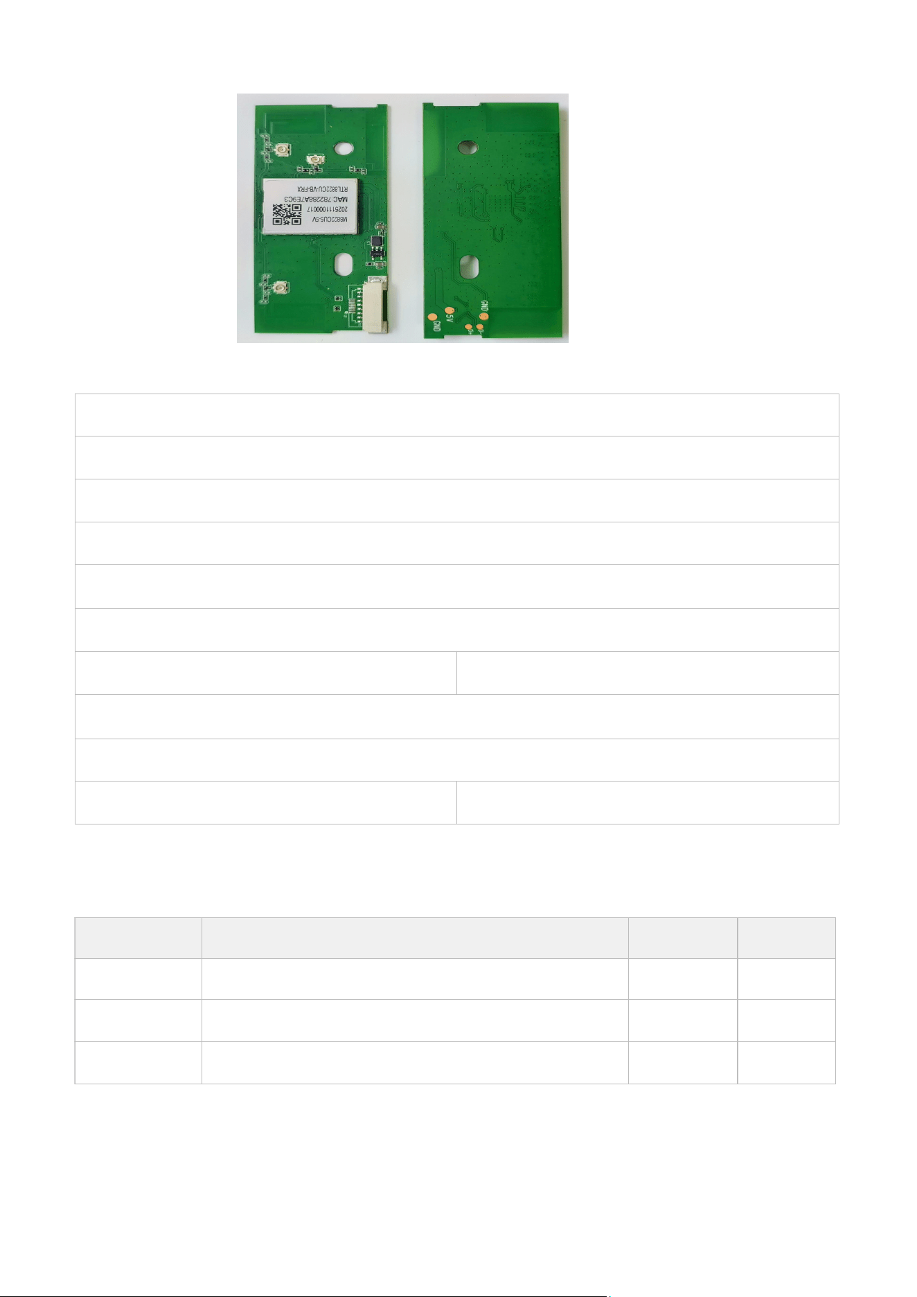
Module Name: FRX-M8822CU5
Module Type: 802.11a/b/g/n/ac 867Mbps WLAN +Bluetooth v5.0 Combo USB2.0 Module
Revision: V1.0
Customer Approval:
Company:
Title:
Signature: Date:
FRX Approval:
Title:
Signature: Date:
Revision History
Revision Summary Release Date Revised By
V0.1 Initial release 2024-01-20 Xhg
V1.0 Official release 2024-04-15 Xhg
2
1. Introduction
FRX-M8822CU5-5V is a highly integrated Dual-band WLAN + Bluetooth v5.0 Combo module. It
combines a 2T2R Dual-band WLAN subsystem and a Bluetooth v5.0 subsystem with USB interface
controller. This module compatible IEEE 802.11 a/b/g/n/ac standard and provides the maximum
PHY rate up to 867Mbps, it supports BT/BLE dual mode with BT v5.0/v4.2/v2.1 compliant, offering
feature-rich wireless connectivity at high standards, and delivering reliable, cost-effective
throughput from an extended distance.
1.1 Features
Operating Frequencies: 2.4~2.4835GHz
Support Dual-band 2T2R mode with 20/40/80MHz bandwidth
Support BT Classic / BT Low Energy dual mode
Power Supply: 5.0±0.5V main power supply
Support IPEX with external antenna
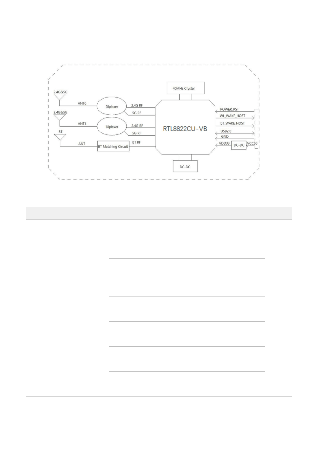
1.2 Block Diagram
3
1.3 General Specifications
Module Name FRX-M8822CU5
Chipset RTL8822CU
WiFi Standard IEEE802.11a/b/g/n/ac
Bluetooth Standard Bluetooth Core Specification v5.0/v4.2/v2.1
Host Interface USB2.0 for WLAN & Bluetooth
Antenna 2 on-board WLAN antennas and 1 on-board BT antenna
Dimension 70.0mm*30.0mm*5.4mm (L*W*H)
Power Supply DC 5.0V±0.5V@ 1A (Max)
Operation Temperature -20℃ to +70℃
Operation Humidity 10% to 95% RH (Non-Condensing)
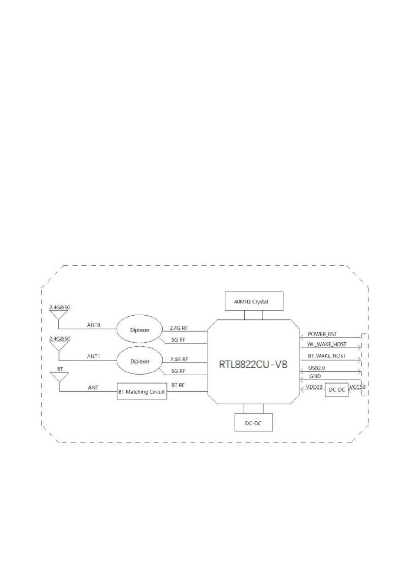
2. Pin Assignments
2.1 Pin Definition
No. Pin Name Type I/O Level Module Pin Description
1 GND P
/
Ground for Power and I/O
2 D+ I/O /
USB Communicat ion signal USB-DP
3 D- I/O
/
USB Communicat ion signal USB-DM

4
4 VCC I 3.3V
VCC3.3V
5 VCC I 3.3V
VCC3.3V
6 VCC I
3.3V
VCC3.3V
7 WL_HOST_WAKE O / WL WAKEUP
8 RESET I /
Reset Controlled by main SOC
9 GND P
/
Ground for Power and I/O
P: Power, I: Input, O: Output, I/O: In/Output, RF: Analog RF Port, A I/O: Analog In/Output
3. Electrical and Thermal Specifications
3.1 Recommended Operating Conditions
Parameters Min Typ Max Units
Ambient Operating Temperature -20 25 70 ℃
Supply Voltage VCC50
4.5 5.0 5.5 V
3.2 Digital I/O DC Specifications
Symbol Parameter Min Typ Max Units
VIH Input High Voltage 2.0 3.3 3.6 V
VIL Input Low Voltage -- 0 0.9 V
VOH Output High Voltage 2.97 -- 3.3 V
VOL
Output Low Voltage
0 -- 0.33 V
5
3.3 Antenna Specifications
Items Frequency Range Gain(max) VSWR polarization
2.4G WLAN /5G
WLAN ANT0
2.4~2.4835GHz(2.4GHz ISM Band)
5.15~5.835GHz(5GHz ISM Band)
3.0dBi <2 Linear polarization
2.4G WLAN /5G
WLAN ANT1
2.4~2.4835GHz(2.4GHz ISM Band)
5.15~5.835GHz(5GHz ISM Band)
3.0dBi <2 Linear polarization
2.4G BT ANT 2.4~2.4835GHz(2.4GHz ISM Band) 3.0dBi <2 Linear polarization
3.4 Current Consumption
Conditions : VCC50=5.0V ; Ta:25℃
Use Case
VCC50 Current
Typ(IRMS) Max(IPeak) Units
WLAN Radio Off (Linux Driver) 20 38 mA
WLAN Unassociated (Linux Driver) 92 128 mA
2.4G WLAN throughput TX 270Mbps(Linux Driver) 310 640 mA
2.4G WLAN throughput RX 270Mbps(Linux Driver) 115 132 mA
5G WLAN throughput TX 300Mbps(Linux Driver) 160 370 mA
5G WLAN throughput RX 300Mbps(Linux Driver) 120 140 mA
2.4G 11b_1Mbps TX@17dBm (1TX RF Test) 230 278 mA
2.4G 11g_6Mbps TX@16dBm(1TX RF Test) 245 340 mA
2.4G 11n_HT20_MCS0 TX@16dBm (1TX RF test) 163 308 mA
2.4G 11n_HT20_MCS7 TX@14dBm (1TX RF test) 162 310 mA
2.4G 11n_HT20_MCS7 RX (1RF test) 119 130 mA
2.4G 11n_HT40 MCS8 TX@16dBm (2TX RF test) 326 652 mA
2.4G 11n_HT40_MCS15 TX@14dBm(2TX RF Test) 196 584 mA
2.4G 11n_HT40_MCS15 RX (2RX RF Test) 144 169 mA
5G 11a_6Mbps TX @16dBm (1TX RF Test) 317 448 mA
5G 11n_HT20_MCS0 TX @16dBm (1TX RF test) 312 444 mA
6
5G 11n_HT20_MCS7 TX @14dBm (1TX RF test) 191 404 mA
5G 11n_HT20_MCS7 RX (1RF test) 135 144 mA
5G 11n_HT40_MCS8 TX@16dBm(2TX RF Test) 435 912 mA
5G 11n_HT40_MCS15 TX@14dBm (2TX RF Test) 239 800 mA
5G 11n_HT40_MCS15 RX (2RX RF Test) 165 191 mA
5G 11ac_VHT80_MCS0 TX@15dBm(2TX RF Test) 235 416 mA
5G 11ac_VHT80_MCS9 TX@13dBm(2TX RF Test) 170 388 mA
5G 11ac_VHT80_MCS9 RX ( 1RF test) 127 150 mA
BT BR_1M TX@6dBm (BT RF test) 205 242 mA
BT EDR_3M TX@6dBm (BT RF test) 208 230 mA
BT LE_1M TX@6dBm (BT RF test) 201 232 mA
BT LE_1M RX Active (BT RF test) 172 178 mA
4. WLAN & Bluetooth RF Specifications
4.1 2.4G WLAN RF Specification
Conditions: VCC50=5.0V; Ta:25℃
Features Description
WLAN Standard IEEE 802.11b/g/n
Frequency Range 2.4~2.4835GHz (2.4GHz ISM Band)
Modulation
802.11b (DSSS): DBPSK, DQPSK, CCK;
802.11g (OFDM): BPSK, QPSK, 16QAM, 64QAM;
802.11n (OFDM): BPSK, QPSK, 16QAM, 64QAM;
Data Rate
802.11b: 1, 2, 5.5, 11Mbps;
802.11g: 6, 9, 12, 18, 24, 36, 48, 54Mbps;
802.11n (HT20): MCS0~MCS7(1T1R_SISO) 6.5~72.2Mbps;
802.11n (HT20): MCS8~MCS15(2T2R_MIMO) 13~144.4Mbps;
802.11n (HT40): MCS0~MCS7(1T1R) 13.5~150Mbps;
802.11n (HT40): MCS8~MCS15(2T2R) 27~300Mbps;
Frequency Tolerance ≦ ±20ppm
2.4G Transmitter Specifications (TX power of some rates is calibrated, customers can define the target
TX power of other rates by modifying configuration file of the driver software. Customers must define
the TX power same or lower than recommended Target TX Power as below )

7
TX Rate
TX Power
(dBm)
TX Power Tolerance
(dBm)
EVM
(dB)
802.11b@1Mbps
Recommended Target
TX Power : 17
±2 ≦-10
802.11b@11Mbps Calibrated TX Power: 15 ±2 ≦-10
802.11g@6Mbps
Recommended Target
TX Power : 16
±2 ≦-10
802.11g@54Mbps Calibrated TX Power: 14 ±2 ≦-25
802.11n@HT20_MCS0
Recommended Target
TX Power : 16
±2 ≦-10
802.11n@HT20_MCS7 Calibrated TX Power: 14 ±2 ≦-28
802.11n@HT40_MCS0
Recommended Target
TX Power : 16
±2 ≦-10
802.11n@HT40_MCS7 Calibrated TX Power: 14 ±2 ≦-28
2.4G Receiver Specifications
RX Rate
Min Input Level
(Typ. dBm)
Max Input Level
(Typ. dBm)
PER
802.11b@1Mbps -96 -10 < 8%
802.11b@11Mbps -88 -10 < 8%
802.11g@6Mbps -93 -10 < 10%
802.11g@54Mbps -75 -10 < 10%
802.11n@HT20_MCS0 -92 -10 < 10%
802.11n@HT20_MCS7 -72 -10 < 10%
802.11n@HT40_MCS0 -89 -10 < 10%
802.11n@HT40_MCS7 -70 -10 < 10%
4.2 5G WLAN RF Specification
Conditions: VCC50=5.0V; Ta:25℃
Features Description
WLAN Standard IEEE 802.11a/n/ac
Frequency Range
Channel
5.15~5.25GHz; 5.725~5.850GHz
(5GHz ISM Band)
s
Ch36, Ch40, Ch44, Ch48; Ch52~Ch64;
Ch100~Ch140; Ch149~Ch165 (For 20MHz Channels)

8
Modulation
802.11a (OFDM): BPSK, QPSK, QAM16, QAM64;
802.11n (OFDM): BPSK, QPSK, QAM16, QAM64;
802.11ac (OFDM): BPSK, QPSK, QAM16, QAM64, QAM256;
Data Rate
802.11a: 6, 9, 12, 18, 24, 36, 48, 54Mbps;
802.11n (HT20): MCS0~MCS7(1T1R_SISO) 6.5~72.2Mbps;
802.11n (HT20): MCS8~MCS15(2T2R_MIMO) 13~144.4Mbps;
802.11n (HT40): MCS0~MCS7(1T1R) 13.5~150Mbps;
802.11n (HT40): MCS8~MCS15(2T2R) 27~300Mbps;
802.11ac (VHT20): MCS0~MCS8(1T1R) 6.5~86.7Mbps;
802.11ac (VHT20): MCS0~MCS8(2T2R) 13~173.3Mbps;
802.11ac (VHT40): MCS0~MCS9(1T1R)13.5~200Mbps;
802.11ac (VHT40): MCS0~MCS9(2T2R)27~400Mbps;
802.11ac (VHT80): MCS0~MCS9(1T1R)29.3~433.3Mbps;
802.11ac (VHT80): MCS0~MCS9(2T2R)58.5~866.7Mbps;
Frequency Tolerance ≦ ±20ppm
5G Transmitter Specifications (TX power of some rates is calibrated, customers can define the target TX
power of other rates by modifying configuration file of the driver software. Customers must define the
TX power same or lower than recommended Target TX Power as below )
TX Rate
TX Power
(dBm)
TX Power Tolerance
(dBm)
EVM
(dB)
802.11a@6Mbps
Recommended Target
TX Power : 16
±2.0 ≦-10
802.11a@54Mbps Calibrated TX Power: 14 ±2.0 ≦-25
802.11n@HT20_MCS0
Recommended Target
TX Power : 16
±2.0 ≦-10
802.11n@HT20_MCS7
Calibrated TX Power: 14 ±2.0 ≦-28
802.11n@HT40_MCS0
Recommended Target
TX Power : 16
±2.0 ≦-10
802.11n@HT40_MCS7
Calibrated TX Power: 14 ±2.0 ≦-28
802.11ac@VHT80_MCS0
Recommended Target
TX Power : 15
±2.0 ≦-10
802.11ac@VHT80_MCS9 Calibrated TX Power: 13 ±2.0 ≦-32

9
5G Receiver Specifications
RX Rate
Min Input Level
(Typ. dBm)
Max Input Level
(Typ. dBm)
PER
802.11a@6Mbps -91 -10 < 10%
802.11a@54Mbps -74 -10 < 10%
802.11n@HT20_MCS0 -90 -10 < 10%
802.11n@HT20_MCS7 -70 -10 < 10%
802.11n@HT40_MCS0 -88 -10 < 10%
802.11n@HT40_MCS7 -68 -10 < 10%
802.11ac@VHT80_MCS0 -84 -10 < 10%
802.11ac@VHT80_MCS9 -58 -10 < 10%
4.3 Bluetooth RF Specifications
Conditions: VCC50=5.0V; Ta:25℃
Features Description
Bluetooth Specification
Bluetooth Core Specification v5.0/v4.2/v2.1
Frequency Range 2.4~2.4835GHz(2.4GHz ISM Band)
Channels
Bluetooth Classic: Ch0~Ch78 (For 1MHz Channels);
Bluetooth Low Energy: Ch0~Ch39 (For 2MHz Channels);
Power Classes
Bluetooth Classic: Class1;
Bluetooth Low Energy: Class1.5;
Data Rate & Modulation
BR_1Mbps: GFSK;
EDR_2Mbps: π/4-DQPSK;
EDR_3Mbps: 8DPSK;
_
_
LE_1Mbps: GFSK (Uncoded);
LE_2Mbps: GFSK (Uncoded);
Bluetooth Transmitter Specifications
Items Min(dBm) Typ(dBm) Max(dBm)
TX Power
10
BR_1M 2 6 10
EDR_2/3M 2 6 10
LE_1M
2 6 10
LE_2M
2 6 10
BR_1M (DH1) Modulation Characteristics
Δf1avg 140KHz 153.5KHz 175KHz
Δf2avg 115KHz 153.2KHz 175KHz
Δf2max 115KHz 165.5KHz /
Δf2avg/Δf1avg 0.8 1 /
BR_1M (DH1) Initial Carrier Frequency Tolerance
Init Freq Error -75kHz -4.3kHz +75kHz
EDR_3M(3DH5) EDR Carrier Frequency Stability and Modulation Accuracy
ωi -75KHz -5.3KHz +75KHz
ωi+ωo -75KHz -5.4KHz +75KHz
ωo -10KHz 0.8KHz +10KHz
8DPSK RMS DEVM / 0.06 0.13
8DPSK Peak DEVM / 0.12 0.25
LE_1M Modulation Characteristics
Δf1avg 225KHz 250.7KHz 275KHz
Δf2avg 185KHz 252.9KHz 275KHz
Δf2max 185KHz 245.5KHz /
Δf2avg/Δf1avg 0.8 0.98 /
LE_2M Modulation Characteristics
Δf1avg 450KHz 494KHz 550KHz
Δf2avg 370KHz 504KHz 550KHz
Δf2max 370KHz 529KHz /
Δf2avg/Δf1avg 0.8 1.1 /
Bluetooth Receiver Specifications
11
Items
Sensitivity Maximum Input Level
Input Level
(Typ. dBm)
BER
Input Level
(Typ. dBm)
BER
BR_1M -90 ≦0.1% -10 ≦0.1%
EDR_3M -82 ≦0.01% -10 ≦0.1%
Input Level
(Typ. dBm)
PER
Input Level
(Typ. dBm)
PER
LE_1M -90 ≦5% -10 ≦5%
LE_2M -84 ≦5% -10 ≦5%
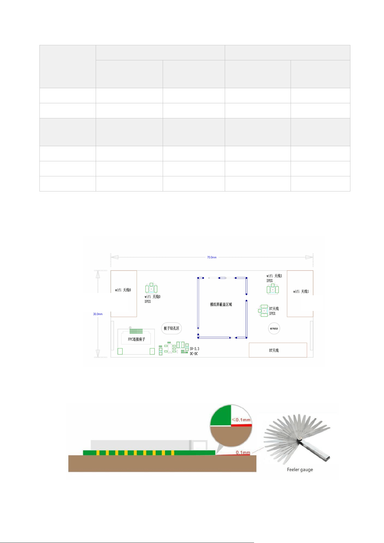
5. Mechanical Specifications
5.1 Module Outline Drawing
Module dimension: 70.0mm*30.0mm*5.4mm (L*W*H; Tolerance: ±0.3mm_L/W, ±0.2mm_H)
Module Bow and Twist:≤0.1mm
12
6. Information
6.1 Typical Application Circuit
7. Key Components Of Module
No. Parts Specification Manufacturer Note
1 Chipset RTL8822CU Realtek Semiconductor Corp.
2 PCB FRX-
M8822CU5-5V
SHEN ZHEN QILI ELECTRON CO.,LTD
Quzhou Sunlord Electronics Co.,Ltd
ShenZhen Tie Fa Technology Limited
3 Crystal 40MHz-3225
LUCKI CM ELECTRONICS CO.,LTD
Chengde oscillator Electronic Technology CO.,LTD
JinHua East Crystal Electronic CO.,LTD
4 Diplexer DP1608
JIA XING GLEAD ELECTRONICS CO., LTD
Shenzhen FTR Technologies CO., LTD
Dongguan Hekang Electronics Co.,LTD
Advanced Ceramic X Corp.
5 DC-DC SOT23-5
Hangzhou Toll Microelectronic Co., LTD
Shenzhen Lowpower Semiconductor Co., LTD
ETA Semiconductor Co., LTD
13
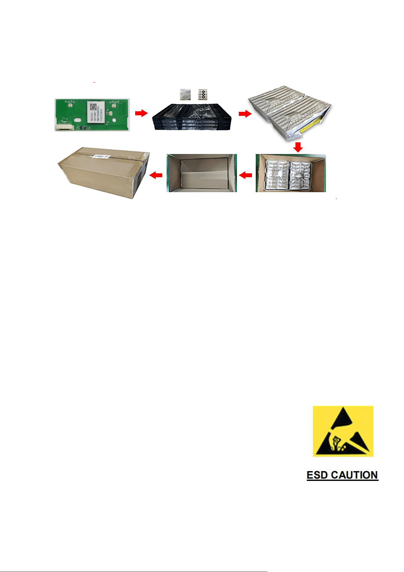
8. Package and Storage Information
8.1 Package Dimensions
Package specification:
1. 12 modules per blister plate and 312modules per box.
2. The blister is bound with wire membrane and put into anti-static vacuum bag.
3. Put 1 bag of dry beads (20g) and 1 humidity card in each anti-static vacuum bag.
4. The outer box size is 43*35.5*16cm.
8.2 Storage Conditions
Absolute Maximum Ratings:
Storage temperature: -40℃ to +85℃
Storage humidity: 10% to 95% RH(Non-Condensing)
Recommended Storage Conditions:
Storage temperature: 5℃ to +40℃
Storage humidity: 20% to 90% RH
Please use this Module within 12month after vacuum-packaged.
The Module shall be stored without opening the packing.
After the packing opened, the Module shall be used within 72hours.
When the color of the humidity indicator in the packing changed,
the Module shall be baked before use.
Baking condition : 60℃, 24hours, 1time.
ESD Sensitivity:
ESD Protection: 2KV(HBM, Maximum rating)
The Module is a static-sensitive electronic device.
Do not operate or store near strong electrostatic fields.
Take proper ESD precautions!

FCC Statement
This device complies with part 15 of the FCC Rules. Operation is subject to the following
two conditions:
(1) This device may not cause harmful interference, and
(2) this device must accept any interference received, including interference that may
cause undesired operation.
This equipment has been tested and found to comply with the limits for a Class B digital
device, pursuant to part 15 of the FCC Rules. These limits are designed to provide
reasonable protection against harmful interference in a residential installation. This
equipment generates, uses and can radiate radio frequency energy and, if not installed
and used in accordance with the instructions, may cause harmful interference to radio
communications. However, there is no guarantee that interference will not occur in a
particular installation. If this equipment does cause harmful interference to radio or
television reception, which can be determined by turning the equipment off and on, the
user is encouraged to try to correct the interference by one or more of the following
measures:
- Reorient or relocate the receiving antenna.
- Increase the separation between the equipment and receiver.
- Connect the equipment into an outlet on a circuit different from that to which the
receiver is connected.
- Consult the dealer or an experienced radio/TV technician for help.
This modular has been tested and found to comply with part 15 requirements for Modular
Approval.
FCC Caution: Any changes or modifications not expressly approved by the party
responsible for compliance could void the user's authority to operate the equipment. This
transmitter must not be co-located or operating in conjunction with any other antenna or
transmitter.
Integration instructions for host product manufacturers according to KDB 996369
D03 OEM Manual v01r01
14
2.2 List of applicable FCC rules
47 CFR FCC Part 15 Subpart C, §15.247 and §15.407 have been fully investigated.
These requirements are applicable to this modular transmitter.

2.3 Specific Operational Use Conditions - Antenna Placement Within the Host
Platform
The module is tested for standalone mobile RF exposure use condition.
● The antenna must be installed such that 20cm is maintained between the antenna and
users,
● The transmitter module may not be co-located with any other transmitter or antenna.
In the event that these conditions cannot be met (for example certain laptop configurations
or co-location with another transmitter), then the FCC authorization is no longer
considered valid and the FCC ID cannot be used on the final product. In these
circumstances, the OEM integrator will be responsible for re-evaluating the end product
(including the transmitter) and obtaining a separate FCC authorization.
2.4 Limited Module Procedures
Not applicable
2.5 Trace Antenna Designs
Not applicable
2.6 RF Exposure Considerations
This device complies with FCC radiation exposure limits set forth for an uncontrolled
environment. This equipment should be installed and operated with minimum distance
20cm between the radiator & your body.
2.7 Antenna Type and Gain
The following antennas have been certified for use with this module.
Only antennas of the same type with equal or lower gain may also be used with this
module.
Other types of antennas and/or higher gain antennas may require the additional
authorization for operation.
Antenna Specification list below:
Model Type Connector
Peak gain ( dBi )
2400-2483.5
MHz
5150-5250
MHz
5250-5350
MHz
5470-5725
MHz
5725-5850
MHz
/ Internal
Antenna
SMA 3.00dBi 3.00dBi / / 3.00dBi
/ Internal
Antenna
SMA 3.00dBi 3.00dBi / / 3.00dBi
/ Internal
Antenna
SMA 3.00dBi / / / /
15

2.8 End Product Labelling Compliance Information
When the module is installed in the host device, the FCC ID label must be visible through
a window on the final device or it must be visible when an access panel, door or cover is
easily removed. If not, a second label must be placed on the outside of the final device
that contains the following text: “Contains FCC ID: 2AVEDFRX-M8822CU5”. The FCC
ID can be used only when all FCC compliance requirements are met.
2.9 Information on Test Modes and Additional Testing Requirements
This transmitter is tested in a standalone mobile RF exposure condition and any
co-located or simultaneous transmission with other transmitter(s) class II permissive
change re-evaluation or new FCC authorization.
Host manufacturer installed this modular with single modular approval should perform the
test of radiated emission and spurious emission according to FCC part 15C, Part 15E,
15.209, 15.207 requirement, only if the test result comply with FCC part 15C, Part 15E,
15.209, 15.207 requirement, then the host can be sold legally
.
2.10 Additional testing, Part 15 Subpart B Disclaimer
This transmitter modular us tested as a subsystem and its certification does not cover the
FCC Part 15 Subpart B rules requirement applicable to the final host. The final host will
still need to be reassessed for compliance to this portion of rules requirements if
applicable.
As long as all conditions above are met, further transmitter test will not be required.
However, the OEM integrator is still responsible for testing their end-product for any
additional compliance requirements required with this modular installed.
2.11 Manual Information to The End User
The OEM integrator has to be aware not to provide information to the end user regarding
how to install or remove this RF module in the user’s manual of the end product which
integrates this module.
The host integrator must follow the integration instructions provided in this document and
ensure that the composite system end product complies with the requirements by a
technical assessment or evaluation to the rules and to KDB Publication 996369.
The host integrator installing this module into their product must ensure that the final
composite product complies with the requirements by a technical assessment or
evaluation to the rules, including the transmitter operation and should refer to guidance in
KDB Publication 996369.
OEM/Host Manufacturer Responsibilities
OEM/Host manufacturers are ultimately responsible for the compliance of the Host and
Module. The final product must be reassessed against all the essential requirements of
the FCC rule such as FCC Part 15 Subpart B before it can be placed on the US market.
16

This includes reassessing the transmitter module for compliance with the Radio and RF
Exposure essential requirements of the FCC rules.
2.12 How to Make Changes - Important Note
In the event that these conditions cannot be met (for example certain laptop configurations
or co-location with another transmitter), then the FCC authorization is no longer
considered valid and the FCC ID cannot be used on the final product. In these
circumstances, the OEM integrator will be responsible for re-evaluating the end product
(including the transmitter) and obtaining a separate FCC authorization.
17