
晶訊科技股份有限公司
8F, No. 150, Jian Yi Road, ZhongheDistrict,
CC&C Technologies, Inc.
New Taipei City, Taiwan235, R.O.C.
Tel: 886-2-8226-5088 Fax: 886-2-8226-5077
1
BM-3095
Bluetooth v5.4 APTX LE Audio
RX Module
Manual
Version: 1.0

晶訊科技股份有限公司
8F, No. 150, Jian Yi Road, ZhongheDistrict,
CC&C Technologies, Inc.
New Taipei City, Taiwan235, R.O.C.
Tel: 886-2-8226-5088 Fax: 886-2-8226-5077
2
Overview
BM-3095 is a highly integrated single-chip Bluetooth v5.4, audio and
programmable application module. It includes high-performance, analog, and
digital audio codes, advanced power management, Li-ion battery charger,
light-emitting diode (LED) drivers, and flexible interfaces incuding
inter-integrated circuit sound (I2S), inter-integrated circuit interface (I2C),
universal asynchronous receiver transmitter (UART), and programmable
input/output (PIO).
The system-on-chip architecture design of the module makes a much smaller
space and minimal cost and simplifies the whole system design.
Features
Qualified to Bluetooth v5.4 specification
Qualcomm® aptX™ and aptX
HD Audio
240 MHz Qualcomm®
Kalimba™ audio DSP
32/80 MHz Developer Processor for applications
Firmware Processor for system
Flexible QSPI flash programmable platform
High-performance 24-bit stereo
Digital and analog microphone interfaces
Flexible LED controller and LED pins with PWM support
Serial interfaces: UART, Bit
Serializer (I²C/SPI), USB 2.0
Advanced audio algorithms
aptX Adaptive, enabled using license key
Integrated PMU: Dual SMPS for system/digital circuits, Integrated Li-ion
battery charger
Application subsystem
Dual-core application subsystem 32/80 MHz operation
32-bit Firmware Processor (reserved for system use) executes:
□ Bluetooth upper stack
□ Profiles
□ House-keeping code
32-bit Developer Processor executes:
□ Developer applications
Both cores execute code from external flash memory using QSPI clocked
at 32 MHz or 80 MHz
晶訊科技股份有限公司
8F, No. 150, Jian Yi Road, ZhongheDistrict,
CC&C Technologies, Inc.
New Taipei City, Taiwan235, R.O.C.
Tel: 886-2-8226-5088 Fax: 886-2-8226-5077
3
On-chip caches per core enable optimized performance
and power
consumption
Bluetooth subsystem
Qualified to Bluetooth v5.4 specification including 2 Mbps Bluetooth Low
Energy and Bluetooth Low Energy Isochronous Channels
Qualcomm® Bluetooth High Speed Link
Single ended antenna connection with on-chip balun and Tx/Rx switch
Bluetooth, Bluetooth Low Energy, and mixed topologies supported
Class 1 support
Application
Bluetooth Receiver with multiple audio interfaces (e.g.,Line in/ Dual
Analog Mic,DigMic,I2S/PCM……..)
General Specification
Model Name BM-3095
Product Name Bluetooth V5.4 APTX LE Audio RX Module
Standard Bluetooth V5.4
Bluetooth Chip QCC3095 WLCSP
Frequency Band 2402MHz ~ 2480MHz
RF Output Power EDR(8DPSK)Mode:9.66dBm
Receiver Sensitivity < -70dBm
Antenna External Antenna
Power supply
VDD_PADS_6: 1.8~3.3V; VDD_PADS_134: 1.8~3.3V;
VBAT:2.8~4.3V
Operating Temperature
-30 ~ +70℃ ambient temperature
Storage Temperature
-40 ~ +85℃ ambient temperature
Humidity
5 to 90 % maximum (non-condensing)
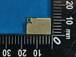
Size 16mm x 11mm x2.5mm (LxWxT)
晶訊科技股份有限公司
8F, No. 150, Jian Yi Road, ZhongheDistrict,
CC&C Technologies, Inc.
New Taipei City, Taiwan235, R.O.C.
Tel: 886-2-8226-5088 Fax: 886-2-8226-5077
4
Factory options
Pin outs define:
◄ PIN 1

晶訊科技股份有限公司
8F, No. 150, Jian Yi Road, ZhongheDistrict,
CC&C Technologies, Inc.
New Taipei City, Taiwan235, R.O.C.
Tel: 886-2-8226-5088 Fax: 886-2-8226-5077
5
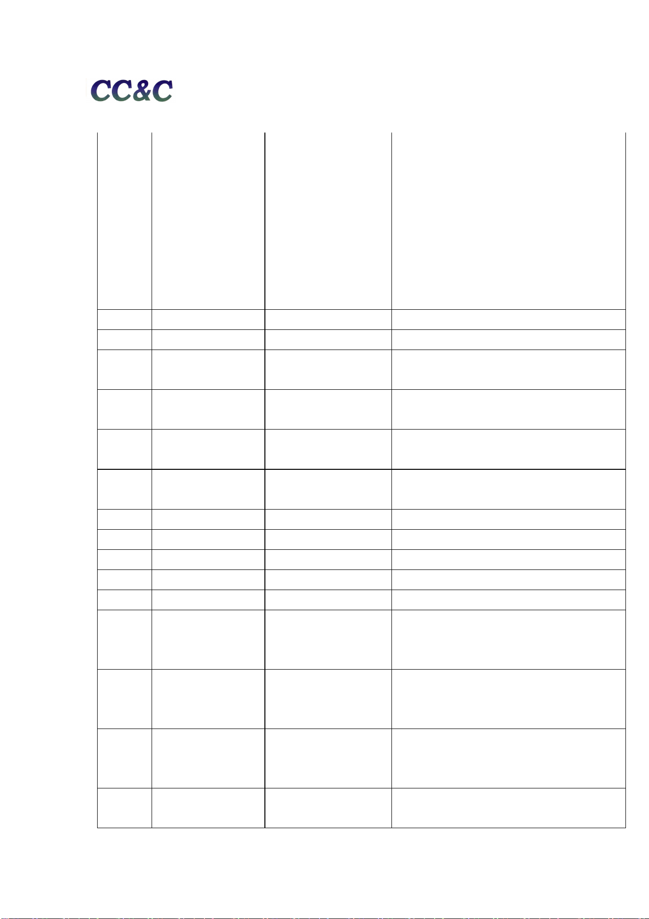
Pin Pin Name Pad Type Description
1 MIC_4_P Analog
Microphone differential 4 input, positive.
Alternative function:
■Differential audio line input 4 , positive
2 MIC_4_N Analog
Microphone differential 4 input, negative.
Alternative function:
■Differential audio line input 4, negative
3 PIO20
Digital: Bidirectional with
programmable strength
internal pull-up/pull-down
Programmable I/O line 20.
Alternative function:
■PCM_DOUT[1]
4 PIO19
Digital: Bidirectional with
programmable strength
internal pull-up/pull-down
Programmable I/O line 19.
Alternative function:
■PCM_DIN[0]
5 PIO18
Digital: Bidirectional with
programmable strength
internal pull-up/pull-down
Programmable I/O line 18.
Alternative function:
■PCM_DOUT[0]
6 PIO17
Digital: Bidirectional with
programmable strength
internal pull-up/pull-down
Programmable I/O line 17.
Alternative function:
■PCM_SYNC
7 PIO16
Digital: Bidirectional with
programmable strength
internal pull-up/pull-down
Programmable I/O line 16.
Alternative function:
■PCM_CLK
8 PIO15
Digital: Bidirectional with
programmable strength
internal pull-up/pull-down
Programmable I/O line 15.
Alternative function:
■MCLK_OUT
9 VBAT_SENSE Analog Battery voltage sense input.
10 USB_DN Digital I/O USB Full Speed device D- I/O.
11 USB_DP Digital I/O USB Full Speed device D+ I/O.
12 VCHG Supply Charger input to Bypass regulator.(USB VBUS)
13 VCHG_SENSE Analog
Charger input sense pin. High impedance.
Connect VCHG_SENSE direct to VCHG.
14 CHG_EXT Analog
External charger transistor current
control. Connect to base of external
charger transistor as per application
schematic.
晶訊科技股份有限公司
8F, No. 150, Jian Yi Road, ZhongheDistrict,
CC&C Technologies, Inc.
New Taipei City, Taiwan235, R.O.C.
Tel: 886-2-8226-5088 Fax: 886-2-8226-5077
6
15 SYS_CTRL Digital input
Typically connected to an ON/OFF push
button. If power is present from the
battery and/or charger, and software has
placed the device in the OFF or
DORMANT state, a button press boots
the device. Also usable as a digital input
in normal operation. No pull.
Additional function:
■ PIO[0] input only
16 VBAT Supply Battery voltage input.
17 GND Ground
18 AIO0/LED0
Analog or digital input
/open drain output.
General-purpose analog/digital input or
open drain LED output.
19 AIO1/LED1
Analog or digital input
/open drain output.
General-purpose analog/digital input or
open drain LED output.
20 AIO2/LED2
Analog or digital
input/open drain output.
General-purpose analog/digital input or
open drain LED output.
21 AIO3/LED3
Analog or digital
input/open drain output.
General-purpose analog/digital input or
open drain LED output.
22 3V3_OUT Supply 3.3V supply output
23 GND Ground
24 1V8_OUT Supply 1.8V supply output
25 VDD_PADS_6 Supply 1.8V/3.3V PIO supply
26 VDD_PADS_134 Supply 1.8V/3.3V PIO supply
27 PIO4
Digital: Bidirectional with
programmable strength
internal pull-up/pull-down
Programmable I/O line 4.
Alternative function:
■TBR_MOSI[1]
28 PIO3
Digital: Bidirectional with
programmable strength
internal pull-up/pull-down
Programmable I/O line 3.
Alternative function:
■TBR_MISO[2]
29 PIO6
Digital: Bidirectional with
programmable strength
internal pull-up/pull-down
Programmable I/O line 6.
Alternative function:
■TBR_MOSI[0]
30 PIO5
Digital: Bidirectional with
programmable strength
Programmable I/O line 5.
Alternative function:

晶訊科技股份有限公司
8F, No. 150, Jian Yi Road, ZhongheDistrict,
CC&C Technologies, Inc.
New Taipei City, Taiwan235, R.O.C.
Tel: 886-2-8226-5088 Fax: 886-2-8226-5077
7
internal pull-up/pull-down
■TBR_MISO[1]
31 PIO8
Digital: Bidirectional with
programmable strength
internal pull-up/pull-down
Programmable I/O line 8.
Alternative function:
■TBR_CLK
32 PIO7
Digital: Bidirectional with
programmable strength
internal pull-up/pull-down
Programmable I/O line 7..
Alternative function:
■TBR_MISO[0]
33 PIO2
Digital: Bidirectional with
programmable strength
internal pull-up/pull-down
Programmable I/O line 2.
Alternative function:
■TBR_MISO[3]
34 PIO1/RST
Digital: Bidirectional with
programmable strength
internal pull-up/pull-down
Automatically defaults to
RESET# mode when the device is unpowered,
or in off modes.
Reconfigurable as a PIO after boot.
Alternative function:
■Programmable I/O line 1
35 PIO21
Digital: Bidirectional with
programmable strength
internal pull-up/pull-down
Programmable I/O line 21
Alternative function:
■PCM_DOUT[2]
36 SPK_R_N Analog
Headphone/speaker differential 2 output,
negative.
Alternative function:
■Differential 2 line output, negative
37 SPK_R_P Analog
Headphone/speaker differential 2 output,
positive.
Alternative function:
■Differential 2 line output, positive
38 SPK_L_N Analog
Headphone/speaker differential 1 output,
negative.
Alternative function:
■Differential 1 line output, negative
39 SPK_L_P Analog
Headphone/speaker differential 1 output,
positive.
Alternative function:
■Differential 1 line output, positive

晶訊科技股份有限公司
8F, No. 150, Jian Yi Road, ZhongheDistrict,
CC&C Technologies, Inc.
New Taipei City, Taiwan235, R.O.C.
Tel: 886-2-8226-5088 Fax: 886-2-8226-5077
8
40 GND Ground
41 MIC_BIAS Analog Mic bias output.
42 MIC_2_N Analog
Microphone differential 2 input, negative.
Alternative function:
■Differential audio line input 2, negative
43 MIC_2_P Analog
Microphone differential 2 input, positive.
Alternative function:
■Differential audio line input 2, positive
44 MIC_1_N Analog
Microphone differential 1 input, negative.
Alternative function:
■Differential audio line input 1, negative
45 MIC_1_P Analog
Microphone differential 1 input, positive.
Alternative function:
■Differential audio line input 1, positive
46 GND Ground
47 MIC_3_N Analog
Microphone differential 3 input, negative.
Alternative function:
■Differential audio line input 3, negative
48 MIC_3_P Analog
Microphone differential 3 input, positive.
Alternative function:
■Differential audio line input 3, positive
49 PIO39
Digital: Bidirectional with
programmable strength
internal pull-up/pull-down
Programmable I/O line 39.
Alternative function:
■QSPI2_IO[3]
50 PIO38
Digital: Bidirectional with
programmable strength
internal pull-up/pull-down
Programmable I/O line 38.
Alternative function:
■QSPI2_CS0#
51 GND Ground
52 RF_OUT RF Bluetooth transmit/receive.
53 GND Ground
54 PIO37
Digital: Bidirectional with
programmable strength
internal pull-up/pull-down
Programmable I/O line 37.
Alternative function:
■QSPI2_IO[1]
55 PIO36
Digital: Bidirectional with
programmable strength
Programmable I/O line 36.
Alternative function:
晶訊科技股份有限公司
8F, No. 150, Jian Yi Road, ZhongheDistrict,
CC&C Technologies, Inc.
New Taipei City, Taiwan235, R.O.C.
Tel: 886-2-8226-5088 Fax: 886-2-8226-5077
9
internal pull-up/pull-down
■QSPI2_IO[2]
56 PIO35
Digital: Bidirectional with
programmable strength
internal pull-up/pull-down
Programmable I/O line 35.
Alternative function:
■QSPI2_CLK
57 PIO34
Digital: Bidirectional with
programmable strength
internal pull-up/pull-down
Programmable I/O line 34.
Alternative function:
■QSPI2_IO[0]
58 XTAL_CLKOUT Analog Buffered clock output.
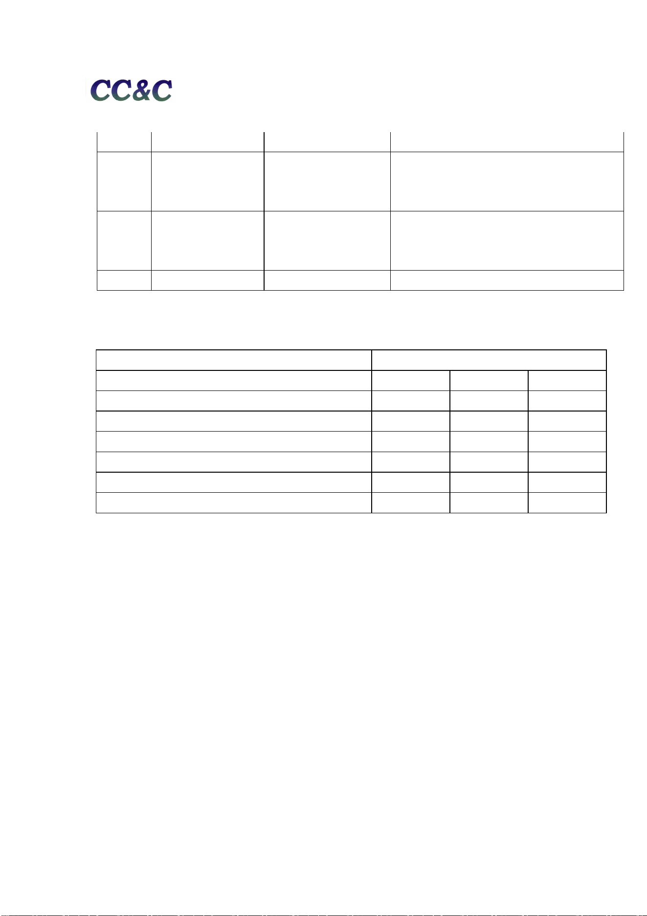
Recommended Operating Conditions Unit: Voltage
Operating Condition Min Type Max
Supply voltage: VCHG (pin 12) 4.75 5 5.5
Supply voltage: VBAT (pin 16) 2.8 3.7 4.3
Supply voltage: VDD_PADS_134 (pin 26) 1.7 1.8 3.6
Supply voltage: VDD_PADS_6 (pin 25) 1.7 1.8 3.6
Supply voltage: SYS_CTRL (pin 15) – 0.4 --- 4.6
Supply voltage: AIO(AIO Mode) 0 --- 1.95
晶訊科技股份有限公司
8F, No. 150, Jian Yi Road, ZhongheDistrict,
CC&C Technologies, Inc.
New Taipei City, Taiwan235, R.O.C.
Tel: 886-2-8226-5088 Fax: 886-2-8226-5077
10
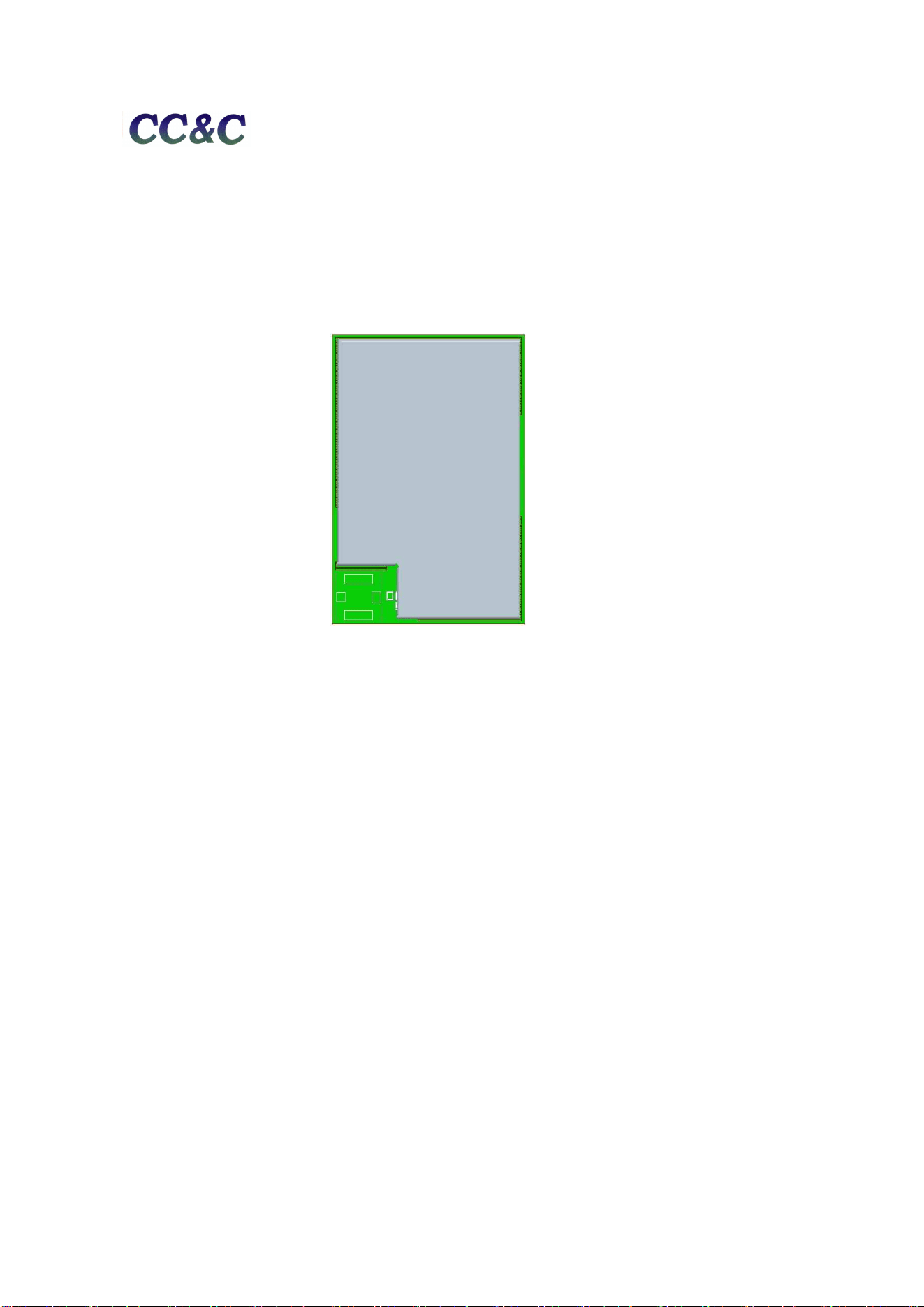
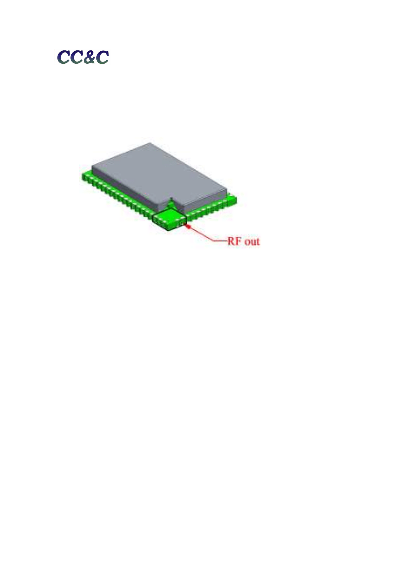
Placement Notice
In order to get a better RF performance, please don’t put any trace or
copper plane under Black frame of the module.
RF out
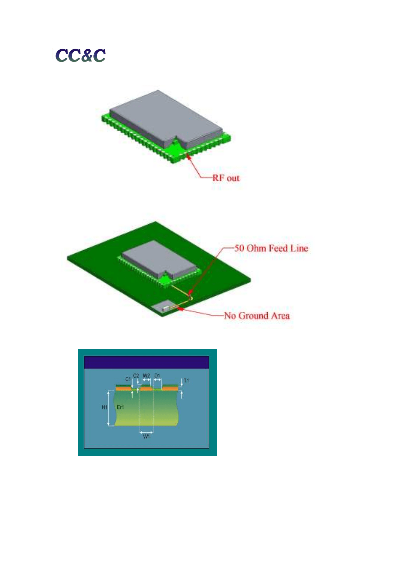
Please have the impedance of feed lines to be 50 ohms from RF output pin to
Antenna.
晶訊科技股份有限公司
8F, No. 150, Jian Yi Road, ZhongheDistrict,
CC&C Technologies, Inc.
New Taipei City, Taiwan235, R.O.C.
Tel: 886-2-8226-5088 Fax: 886-2-8226-5077
11
50 Ohm Feed line:
H1: 20 ~ 60 mil
Er1: 4.2
W1: 20 mil
W2: 20 mil
D1: 5 mil
C1: 0.7 mil
C2: 0.7 mil
T1: 1.4 mil (1 oz)
Impedance: 51 ~ 53 O
晶訊科技股份有限公司
8F, No. 150, Jian Yi Road, ZhongheDistrict,
CC&C Technologies, Inc.
New Taipei City, Taiwan235, R.O.C.
Tel: 886-2-8226-5088 Fax: 886-2-8226-5077
12
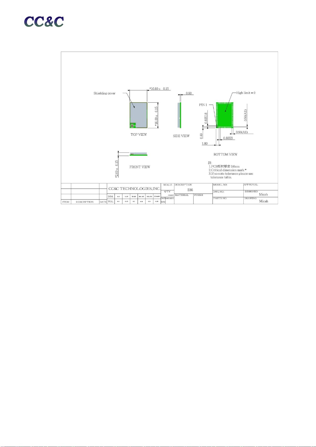
Dimension
Subject to change without notice
晶訊科技股份有限公司
8F, No. 150, Jian Yi Road, ZhongheDistrict,
CC&C Technologies, Inc.
New Taipei City, Taiwan235, R.O.C.
Tel: 886-2-8226-5088 Fax: 886-2-8226-5077
13
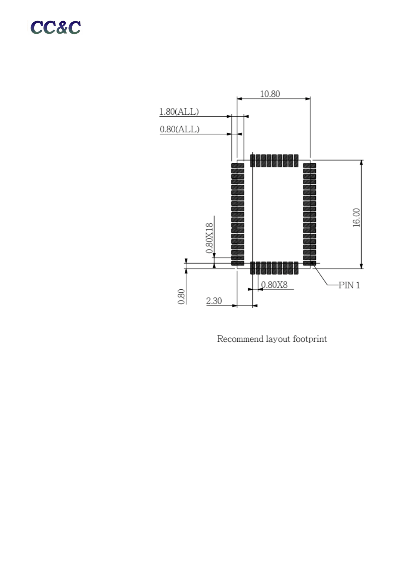
PCB Layout footprint
The recommended layout pads for BM-3095 module are shown below.
All dimensions are in millimeters.
晶訊科技股份有限公司
CC&C
Technologies, Inc.
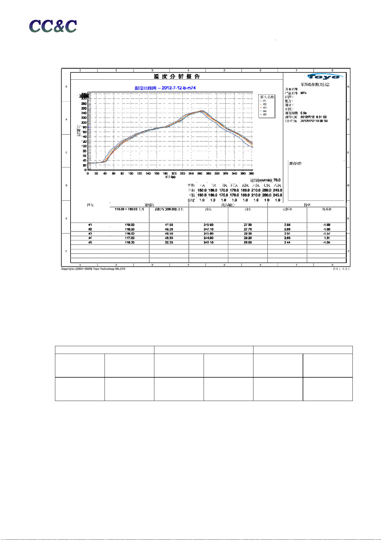
Reference Temperature Reflow Chart
Note:
1. If the system
PCBA is double side design please reflow the side without this module first.
2. Don’t let the solder machine temperature over 250
3. The Ramp-
up temperature speed is 1~4
4. This temperature reflow chart is for reference only, it depends on the manufaturing machine’s characters requirement.
This module is surface mount device; please refer below conditions
(extracted from IPC/JEDEC J-STD
-
Bake @ 125
o
C
Exceeding
floor Life
By > 72h
Exceeding
floor Life
By ≤ 72h
9 hours
7 hours
晶訊科技股份有限公司
8F, No. 150, Jian Yi Road, ZhongheDistrict,
Technologies, Inc.
New Taipei City, Taiwan
235, R.O.C.
Tel: 886-2-8226-
5088 Fax: 886
14
Reference Temperature Reflow Chart
PCBA is double side design please reflow the side without this module first.
2. Don’t let the solder machine temperature over 250
℃ or follow solder paste vender’s
recommended temperature.
up temperature speed is 1~4
o
C per second, the Ramp-
down temperature speed is 1~4
4. This temperature reflow chart is for reference only, it depends on the manufaturing machine’s characters requirement.
This module is surface mount device; please refer below conditions
for drying before
-
033B.1)
Bake @ 90
o
C
Exceeding
floor Life
≤ 72h
Exceeding
floor Life
By > 72h
Exceeding
floor Life
By ≤ 72h
Exceeding
floor Life
By > 72h
7 hours
33 hours
23 hours
13 days
8F, No. 150, Jian Yi Road, ZhongheDistrict,
235, R.O.C.
5088 Fax: 886
-2-8226-5077
PCBA is double side design please reflow the side without this module first.
recommended temperature.
down temperature speed is 1~4
o
C per second.
4. This temperature reflow chart is for reference only, it depends on the manufaturing machine’s characters requirement.
for drying before
solder reflow processes.
Bake @ 40
o
C
Exceeding
floor Life
By > 72h
Exceeding
floor Life
By ≤ 72h
13 days
9 days
晶訊科技股份有限公司
8F, No. 150, Jian Yi Road, ZhongheDistrict,
CC&C Technologies, Inc.
New Taipei City, Taiwan235, R.O.C.
Tel: 886-2-8226-5088 Fax: 886-2-8226-5077
15
晶訊科技股份有限公司
8F, No. 150, Jian Yi Road, ZhongheDistrict,
CC&C Technologies, Inc.
New Taipei City, Taiwan235, R.O.C.
Tel: 886-2-8226-5088 Fax: 886-2-8226-5077
16
This device complies with Part15 of the FCC Rules. Operationis subject to the following two
conditions:
(1)
this device may not cause harmful interference, and
(2)
this device must accept any interference received, including interference that may cause
undesired operation.
This equipment has been tested and found to comply with the limits for a Class B digital device,
pursuant to part 15 of the FCC Rules. These limits are designed to provide reasonable protection against
harmful interference in a residential installation. This equipment generates, uses and can radiate radio
frequency energy and, if not installed and used in accordance with the instructions, may cause harmful
interference to radio communications. However, there is no guarantee that interference will not occur in
a particular installation. If this equipment does cause harmful interference to radio or television
reception, which can be determined by turning the equipment off and on, the user is encouraged to try to
correct the interference by one or more of the following measures:
—Reorient or relocate the receiving antenna.
—Increase the separation between the equipment and receiver.
—Connect the equipment into an outlet on a circuit different from that to which the receiver is
connected.
—Consult the dealer or an experienced radio/TV technician for help.
Any changes or modifications not expressly approved by the party responsible for
compliance could void the authority to operate equipment.
This device and its antenna(s) must not be co-located or operating in conjunction with any other
antenna or transmitter.

晶訊科技股份有限公司
8F, No. 150, Jian Yi Road, ZhongheDistrict,
CC&C Technologies, Inc.
New Taipei City, Taiwan235, R.O.C.
Tel: 886-2-8226-5088 Fax: 886-2-8226-5077
17
FCC RF Radiation Exposure Statement:
This equipment complies with FCC RF radiation exposure limits set forth for an uncontrolled
environment.
This equipment should be installed and operated with a minimum distance of 20 centimeters between
the radiator and your body.
晶訊科技股份有限公司
8F, No. 150, Jian Yi Road, ZhongheDistrict,
CC&C Technologies, Inc.
New Taipei City, Taiwan235, R.O.C.
Tel: 886-2-8226-5088 Fax: 886-2-8226-5077
18
Requirement of FCC KDB 996369 D03 for module certification:
2.2 List of applicable FCC rules
This module complies with FCC Part 15.247
2.3 Summarize the specific operational use conditions
The module must be installed with an approved antenna type and maximum gain as specified in this manual.
The module is tested for standalone mobile RF exposure use condition. Any other usage conditions such as co-location
with other transmitter(s) or being used in a portable condition will need a separate reassessment through a class II
permissive change application or new certification.
2.4 Limited module procedures
Not applicable.
2.5
Trace antenna designs: Not applicable, the antennas for this module are integrated into the module.
Use of external antennas or antennas integrated into the host circuit board are not an option
2.6 RF exposure considerations
This equipment complies with FCC radiation exposure limits set forth for an uncontrolled environment. This
equipment should be installed and operated with a minimum distance of 20cm between the radiator & your body.
This transmitter must not be co-located or operating in conjunction with any other antenna or transmitter.
2.7 Antennas:
The following antennas have been certified for use with this module.
Only antennas of the same type with equal or lower gain may also be used with this module.
Other types of antennas and/or higher gain antennas may require the additional authorization for operation.
The installer should use unique antenna connector and Antenna types not included in this list that have a gain
greater than the maximum gain indicated for any type listed are strictly prohibited for use with this device.
The manufacturer of module will inform installer to meet with the FCC part 15.203 in the warning part.
Antenna Specification list below:
Model Name BM-3095
Antenna Type
Chip Antenna
Antenna Gain 0.5dBi
Antenna Brand ACX
Antenna Model
AT3216
-
B2R7HAAT/LF
Connector
N/A
2.8 Label and compliance information
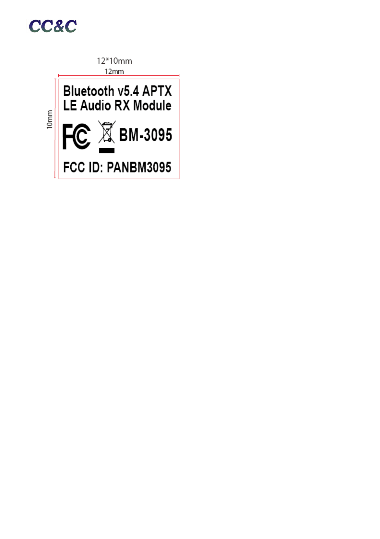
Please notice that if the FCC identification number is not visible when the module is installed inside another
device, then the outside of the device into which the module is installed must also display a label referring to the
enclosed module. This exterior label can use wording such as “Contains FCC ID: PANBM3095”;
any similar wording that expresses the same meaning may be used.
2.9
In accordance with FCC guidance it is recommended that the host product manufacturer perform investigative
measurements to confirm that the system does not exceed the spurious emissions limits or band edge limits
once the module is installed in the host system.
If the host system contains other transmitters additional testing is required to check for emissions that may occur due to the
intermixing of emissions with the other transmitters, digital circuitry, or due to the physical properties of the host product
(enclosure). RF exposure assessments to account for transmissions across all transmitters that can operate simultaneously is also
required.
For additional information refer to FCC KDB 996369 D04 Module Integration Guide.

晶訊科技股份有限公司 8F, No. 150, Jian Yi Road, ZhongheDistrict,
CC&C Technologies, Inc. New Taipei City, Taiwan235, R.O.C.
Tel: 886-2-8226-5088 Fax: 886-2-8226-5077
1
9
2.10
The host product manufacturer is responsible for compliance with any other FCC rules that apply to the
host not covered by the modular transmitter grant of certification.
2.11
The host manufacturer is recommended to use FCC KDB 996369 D04 Module Integration Guide recommending
as" best practice" RF design engineering testing and evaluation in case non-linear interactions generate additional
non-compliant limits due to module placement to host components or properties.
2.12
The module is for specific audio line in like USB, 3.5mm or others. If the end product will involve the
different operations, the host manufacture have to consult with the module manufacture for the
integration method in end system.