
User's manual
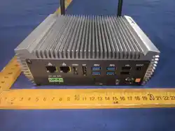
SIN-3095-N95

This manual is for reference only and is subject to change without prior notice. The company shall
not be liable for direct, indirect, special, incidental or consequential damages arising from the use of the
product or document, or for any infringement of third-party rights. When the equipment is in operation, the
equipment can generate, use and radiate radio frequency energy, which may cause harmful interference
to wireless communications if not installed and used in accordance with the regulations. In this case, th
Disclaimer
e
user needs to consult the company's after-sales service hotline to solve the problem. The
company/product names mentioned in this document are for identification purposes only and are
trademarks or registered trademarks of their respective companies.
Warnings and Notes
Warning! During operation, users must pay special attention to the warning information in this manual to
avoid personal injury.
CAUTION! The cautions in this manual help you avoid hardware damage or data loss, for example:
There is a risk of explosion if the battery is replaced incorrectly.
NOTE! This item provides additional information.
Packing list
Before installing the system, the user needs to confirm that the package contains the device and the
following items, and that the device is in good condition:
2
1xSIN-3095-N95
1xWarranty card
1xPower adapter(DC24V,60W)
1xPower cable
1xHDMl cable
2xWall mount
2xWiFi antenna

Ordering Information
Configuration 1
Intel N95 onboard CPU, 4GB DDR4 Memory, 128GB SSD, 24V 60W adapter
Configuration 2
Intel N95 onboard CPU, 8GB DDR4 Memory, 256GB SSD, 24V 60W adapter
Configuration 3
Intel N95 onboard CPU, 16GB DDR4 Memory, 512GB SSD, 24V 60W adapter
Optional accessories
2018203BBSZ000 Removable baffle (blank)
2018204BBSZ000 Removable baffle A (extending 4 DB9 ports)
3

Safety Instructions
1. Please read these safety instructions carefully.
2. Please keep this user manual for future reference.
3. Before cleaning the device with a wet cloth, please unplug the power cord from the socket. Please do
not use liquids or detergent sprays to clean the device.
4. For devices that use power cords, there must be easily accessible power sockets around the device.
5. Do not use the device in a humid environment.
6. Please make sure that the device is place
d on a reliable surface before installation. Accidental falls may
cause damage to the device.
7. The openings in the device housing are used for air convection to prevent the device from overheating.
Please do not cover these openings.
8. Before you connect the device to the power socket, please confirm that the voltage of the power socket
meets the requirements.
9. Please place the power cord in a position where people are not likely to trip and do not cover the power
cord with any debris.
10. Pay attention to all warning signs on the device.
11. If the device is not used for a long time, please disconnect it from the power socket to prevent the
device from being damaged by excessive voltage fluctuations.
12. Do not let any liquid flow into the vents to avoid fire or short circuit.
13. Please do not open the device by yourself. To ensure your safety, please have a certified engineer
open the device.
14. If you encounter the following situations, please hav
e a professional repair:
The power cord or plug is damaged.
Liquid has flowed into the device.
The device has been exposed to excessive humidity.
The device does not work properly, or you cannot make it work properly according to the user manual.
The device has been dropped or damaged.
The device has obvious external damage.
15.Please do not place the device in an environment that exceeds our recommended storage temperature
range, that is, not below -10°C or above 60°C, other
wise the device may be damaged.
16. Note: The computer is equipped with a battery-powered real-time clock circuit. If the battery is not
replaced correctly, there is a risk of explosion. Therefore, only use the same or equivalent type of battery
recommended by the manufacturer for replacement. Please dispose of old batteries according to the
manufacturer's instructions.
17. Restricted access area: The device can only be installed in a restricted access area.
4

Disclaimer................................................................................................................................................................................................... 2
Warnings and Notes....................................................................................................................................................................................2
Packing list..................................................................................................................................................................................................2
Ordering Information............................................................................................................................................................................
........3
Optional accessories................................................................................................................................................................................... 3
Safety Instructions.......................................................................................................................................................................................4
1 Device Port Description............................................................................................................................................................................
Tableofcontents
6
1.1 、Product appearance dimensions................................................................................................................................................ 6
1.2 Front panel I/O in
terface................................................................................................................................................................ 8
1.3 Rear panel I/O interface.................................................................................................................................................................8
1.4 Machine weight..............................
...............................................................................................................................................8
1.5 Overall size...................................................................................................................................................................................8
1.6 power supply................................................
................................................................................................................................ 8
1.7 Ambient temperature..................................................................................................................................................................... 8
2 Models and Attentions ............................................................................................................................................................................. 9
1.1 Model..........................................................................................................................................................................................9
1.2 Attentions..................................................................................
...................................................................................................9
3 Specification..........................................................................................................................................................................................10
4 Block Diagram.....................................................................................
.................................................................................................. 14
5 Mechanical Drawing.............................................................................................................................................................................. 15
6 Headers / Wafers and Connectors......................................................................................................................................................... 16
7 Definition of Connectors.........................................................................................................................................................................19
7.1 DC Power Input 24V: Terminal Block, 2*1P, 3.50mm (Mark No.3, DC_IN2)....................................................................
...............19
7.2 eDP/LVDS Backlight Control: Wafer, 6*1P, 2.00mm (Mark No.7, LVDS_P1)................................................................................. 19
7.3 LVDS VDD Select: Jumper,3*2P, 2.54mm (Mark No.8, JV_LVDS1)..........................................................................................19
7.4 eDP/LVDS Signal: Wafer, 20*2P, 1.25mm (Mark No.9, LVDS1).......................................
............................................................ 19
7.5 Amplifier: Wafer, 2*1P, 1.25mm (Mark No.10, J_SPK1)................................................................................................................20
7.6 SATA Power: Wafer, 4*1P, 2.00mm (Mark No.12, P_SATA1).......................................................................................................20
7.7 SIM Card: Wafer, 6*1P,
1.25mm (Mark No.16, J_SIM1)............................................................................................................... 20
7.8 GbE LAN: RJ45 Connector (Mark No.17, LAN1).......................................................................................................................... 21
7.9 GbE LAN: RJ45 Connector (Mark No.18, LAN2).......................................................................................................................... 21
7.10 Front USB2.0: Wafer, 5*2P, 2.00mm (Mark No.22, F_USB1)......................................................................................................21
7.11 Front USB2.0: Wafer, 4*1P, 2.00mm (Mark No.23, F_USB2)......................................................................................................21
7.12 Front USB2.0: Wafer, 4*1P,
2.00mm (Mark No.24, F_USB3)......................................................................................................22
7.13 COM1: Wafer, 9*1P, 1.25mm (Mark No.25, J_COM1) ................................................................................................................22
7.14 COM2: Wafer, 9*1P, 1.25mm (Mark No.26, J_COM2) ................................................................................................................22
7.15 COM3: Wafer, 9*1P, 1.25mm (Mark No.27, J_COM3) ................................................................................................................22
7.16 COM4: Wafer, 3*1P, 2.00mm (Mark No.28, J_COM4) ................................................................................................................23
7.17 COM5: Wafer, 3*1P, 2.00mm (Mark No.29, J_C
OM5)................................................................................................................23
7.18 COM6 RS485: Wafer, 3*1P, 2.00mm (Mark No.30, J_COM6_RS1)............................................................................................23
7.19 COM6: Wafer, 3*1P, 2.00mm (Mark No.31, J_COM6) ................................................................................................................23
7.20 Front Panel: Wafer, 4*2P, 2.00mm (Mark No.32, F_PANEL1).....................................................................................................23
7.21 GPIO: Wafer, 5*2P, 2.00mm (Mark No.33, J_GPIO1).................................................................................................................24
7.22 I2C: Wafer, 6*1P, 1.25mm (Mark No.34, J_I2C1)...................
.................................................................................................... 24
7.23 CPU FAN: Wafer, 4*1P, 1.25mm (Mark No.35, CPU_FAN1)...................................................................................................... 24
7.24 Power Debug: Wafer, 4*1P, 1.25mm (Mark No.36, J_PRM1)..................................................................................................... 24
7.25 ESPI Debug: Header, 6*2P, 2.00mm (Mark No.37, J_ESPI1)..................................................................................................... 25
7.26 CMOS Battery: Wafer, 2*1P, 1.25mm (Mark No.38, J_BAT1)..................................................................................................... 25
7.27 CMOS Clear: Jumper,3*1P, 2.54mm (Mark No.39, CLR_CMOS1)..............................................................................................25
8 BIOS Setup ............................................................................................................................................................................................ 26
8.1 Entering Setup............................................................................................................................................................................ 26
8.2 BIOS Menu Screen..................................................................................................................................................................... 27
8.3 Function Keys............................................................................................................................................................................. 27
8.4 Getting Help................................................................................................................................................................................27
8.5 Menu Bars.........................................................................................................................................................................
......... 28
8.6 Main Menu..................................................................................................................................................................................28
8.7 Advanced Menu..........................................................................................................................................................................29
8.8 Chipset M
enu ............................................................................................................................................................................. 33
8.9 Security Menu.............................................................................................................................................................................34
8.10 Boot Menu................................................................................................................................................................................ 35
8.11 Save & Exit Menu......................................................................................................................................................................36
9 Driver Installation ......................................
..............................................................................................................................................36
9.1 Download Driver: ...................................................................................................................................................................... 36
9.2 Unzip the file:......................................................
......................................................................................................................37
9.3 Run the installer: .......................................................................................................................................................................37
9.4 Restart your computer:..............................................................................................................................................................39
9.5 Check the driver:...................................................................................................................................................................... 39
10 Network and WiFi connections................................................................................................
..............................................................40
10.1 Network connection:............................................................................................................................................................... 40
10.2 WiFi connection:......................................................................................................................................
............................... 41
5
1、Device Port Description
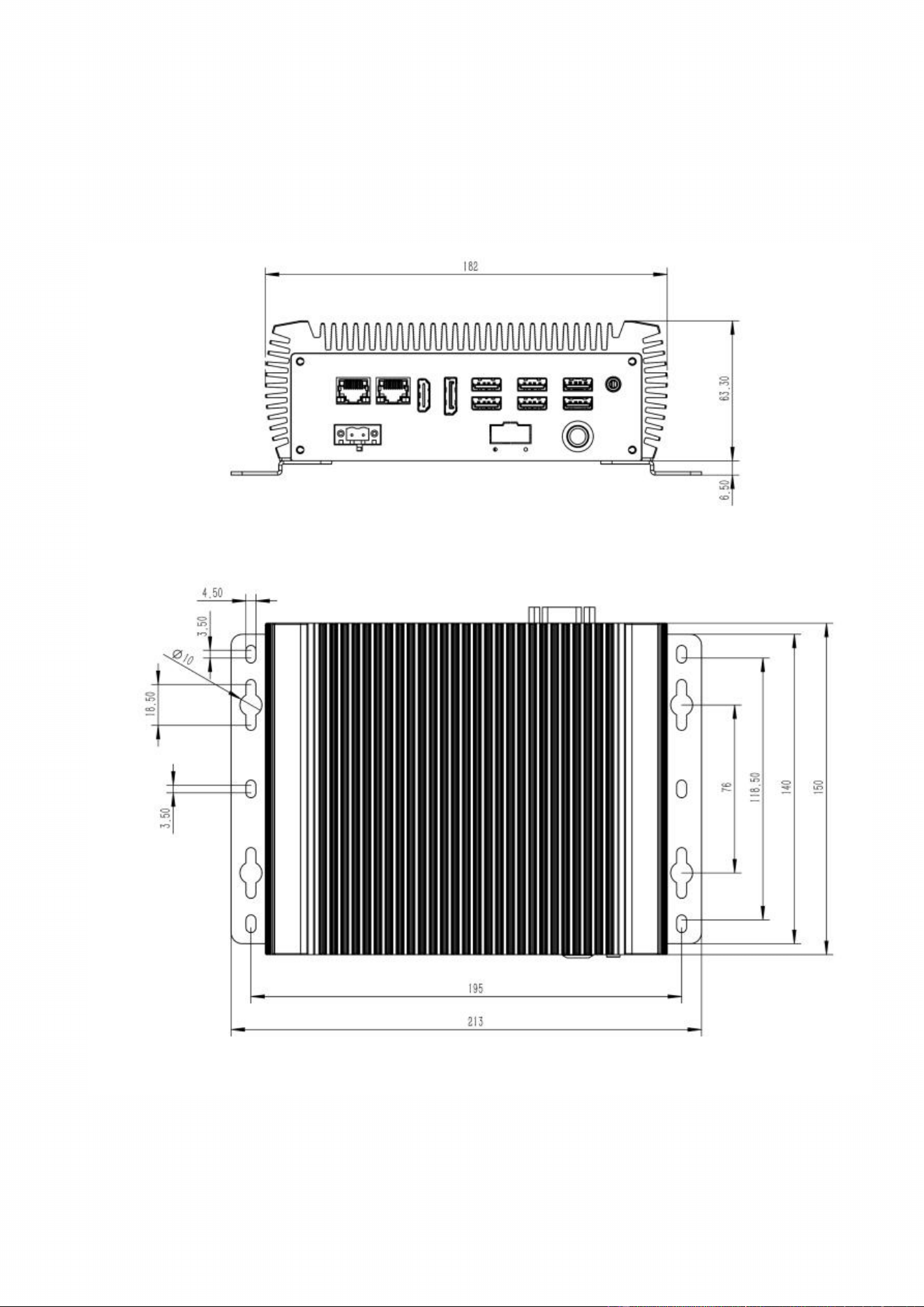
1.1、Product appearance dimensions
(
Dimensions
)
6

7
(
Interface Description
)

1.2 Front panel I/O interface
Host Switch:
The host switch is a tactile switch for ATX mode on/off operation. To power on the controller, open the
front panel cover and press the "POWER" button; the POWER LED will illuminate. To shut down the
controller, issue a shutdown command in the operating system or press the "POWER" button. If the
system is stopped, press and hold the power button for 5 seconds to shut it down. It's important to note
that after shutting down the industrial
computer, wait at least 5 seconds before restarting it (i.e., once
shutting down the system, wait 5 seconds before pressing the power button to restart).
USB3.2*4/USB2.0*2:
High-speed USB data transmission port for connecting USB storage devices and plug-and-play USB
devices.
RJ45*2:
This network port is a high-speed Gigabit Ethernet port, providing connectivity to the Internet. One of the
ports can transmit data at up to 2.5 Gbps.
HDMI*1:
You can connect an HDMI-enab
led monitor to this port. HDMI technology supports resolutions up to
4096x2160@30Hz; the actual supported resolution may vary depending on the monitor.
DP*1:
You can connect a DP-enabled monitor to this port. DP technology supports resolutions up to
4096x2160@60Hz; the actual supported resolution may vary depending on the monitor.
Audio*1:
This port is a 3.5mm two-in-one audio jack (Line Out + Mic In).
Power In:
Power the device via an adapter.
1.3 Rear panel I/O interfa
ce
Serial Ports*6:
Used for connecting computer serial interface peripherals. Connecting cables and mechanical,
electrical characteristics, signal functions, and transmission.
1.4 Machine weight
Net weight about 1.8KG
1.5 Overall size
182*150*63.3mm (width*depth*height)
1.6 power supply
Power Input: 24VDC
60W adapter 24V/2.5A (included in accessory box)
1.7 Ambient temperature
Operating Temperature:
-10~60°C (-10~60°C), with airflow at 0.7m/s
Relative H
umidity:
5~95% @ 40°C (non-condensing)
Storage Temperature:
-20~75°C
8

2 Models and Attentions
1.1 Model
This manual is applied to following models:
1.2 Attentions
1) Notes under a table or figure indicate the difference of models, or alternative definition of specific pin of the
header (jumper/connector).
2) How to identify the first pin of a header or jumper
◼ Usually, there is a thick line or a triangle near the header’s or jumper’s pin 1.
◼ Square pad, which you can find on the back of the motherboard, is usually used for pin 1.
Model CPU COM LAN USB DP HDMI
LVDS
/eDP
M.2
Key-B
M.2
Key-E
M.2
Key-M
SATA
3.0
N95 7 2 9 1 1 LVDS
USB3.0+
USB2.0
PCIE+
USB2.0
NVMe
/SATA
SSD
0
N97 7 2 9 1 1 LVDS
USB3.0+
USB2.0
PCIE+
USB2.0
NVMe
/SATA
SSD
0
N100 7 2 9 1 1 LVDS
USB3.0+
USB2.0
PCIE+
USB2.0
NVMe
/SATA
SSD
0
i3-
N305
7 2 9 1 1 LVDS
USB3.0+
USB2.0
PCIE+
USB2.0
NVMe
/SATA
SSD
0
DTB-3095-
N95L2
DTB-3095-
N97L2
DTB-3095-
N100L2
DTB-3095-
N305L2
9

3 Specification
Specifications
Model
DTX-BN95ME DTX-BN97ME
DTX-
BN100ME
DTX-
BN305ME
Processor
System
Processor
Intel
®
Alder Lake-N Series Processor
N95 N97 N100 i3-N305
Clock Speed
up to 3.40GHz up to 3.60GHz up to 3.40GHz
up to 3.80GHz
Multi-Core
4E-Core
4E-Core 4E-Core 8E-Core
TDP
15W
12W
6W 15W
BIOS AMI UEFI BIOS (Support Watchdog Timer)
Memory
Slot Type
1, DDR4 Non-ECC SO-DIMM
Memory Type
DDR4 3200MHz
Max Memory
16GB
Channels Single
Display
Graphics
Intel
®
UHD Graphics
up to 16 EUs,
1.20 GHz
up to 24 EUs,
1.20 GHz
up to 24 EUs,
750 MHz
up to 32 EUs,
1.25 GHz
HDMI
1, HDMI, max 4096*2160@30Hz
eDP/LVDS
1, LVDS, max 1920*1200@60Hz
Notes:
*: BOM optional support eDP, max 4096*2160@30Hz
Multi-Display Dual
Audio
Codec
Realtek Audio HDA codec
Audio
1, Line-Out + MIC
Storage
M.2 SSD
1, M.2 M-Key 2280, PCIE 2x/SATA, Default SATA, Support SATA SSD
Notice:
*: PCIE signal colay with SATA1 and M.2_KEYB_SSD1. When using
SATA1, M.2_KEYB_SSD1 can only support SATA.
SATA
1, SATA Gen3 6Gbps
Mini-PCIe
1, Mini-PCIe, PCIE+USB2.0, support WIFI+4G Module
SIM Card 1, SIM Crad
Expansion
Slot
10

Interfaces
Model
DTX-BN95ME DTX-BN97ME
DTX-
BN100ME
DTX-
BN305ME
Rear I/O
Power on
1, Button
Ethernet 4, GbE RJ45
HDMI 1, HDMI TYPE-A
USB2.0
2, USB2.0 TYPE-A
USB3.0 2, USB3.0 TYPE-A
Power In
1, 3P 5.08mm Terminal Block
Notes:
*: BOM optional support 2P 3.5mm Terminal Block.
Internal I/O
Display
1, DF13, eDP/LVDS, with Backlight Control Wafer
Audio
1, Wafer, Line-out+ MIC
Storage
1, SATA 7P Port, with Power supply Wafer
1, M.2 M-Key 2280, SATA, support SATASSD
Expansion
1, Mini-PCIe Slot, PCIE+USB2.0, Support WIFI+4G
1, Wafer, SIM Card
1, Board to Board Connector, Expansion Card
1, Header, Expansion Card Power Input
USB2.0
2, Wafer
Serial
1, P Terminal Block, COM1+COM2+Power on
Notice
*: COM1 wafer+COM2 wafer +Power on wafer optional.
GPIO 1, Wafer
Reset
1, Wafer
HDD LED 1, Blue light LED
FAN
1, Wafer, CPU FAN
Others
Jumper
1, LVDS1 VDD Select
1, LVDS1 Blacklight Control Select
2, COM1 RS232/RS485 Select
1, COM1 RS485 Signal 120Ω Resistive termination Select
1, CMOS Clear Select
RTC 1, Wafer
Buzzer
1
11

B2B
1, Expansion Card
1, Expansion Card Power Input
Ethernet
Chipset
4, Intel
®
i210 GbE Ethernet Controller
USB
USB3.0
2, USB3.2 Gen1 5Gbps
USB2.0 2, USB2.0
I/O
Serials
1, RS232/RS485, COM1, default RS232 selected by jumper
1, RS485, COM2, default RS485
Power on
2
Reset
1
HDD LED 1
FAN
—
CMOS Clear 1
GPIO GPIO
—
Power Power in
1, DC 24V Power Input
Notes:
*: BOM optional support 12V.
OS
OS Supported
Windows 10/11 64bit, Linux
Environment
Temperature
Operation: -10 ~ 60℃
Storage: -40 ~ 85℃
Humidity 5 ~ 95%, non-condensing
Dimension
3.5 inch, 146mm*105mm
Height
PCB: 1.6mm
Mechanical
12

13
PWR-ON,RESET
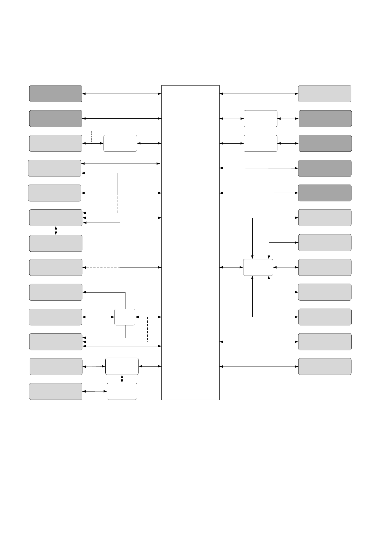
4 Block Diagram
USB2.0(4G)
USB3.0
TTL*3
FAN
GPIO*8
PCIE
USB2.0*2
USB2.0
Wafer
Dual USB2.0
Wafer
USB2.0
SATA/PCIE
SATA/PCIE
PCIE
PCIE
GbE LAN RJ45
LAN RJ45 2.5GbE
8022
Key-MM.2
SATA Port
USB2.0
HUB
SIM Wafer
DIMM-SO
DDR4
Wafer
USB2.0
Converter
Converter
Converter
Super IO
AMP
Audio codec
3022
Key-EM.2
2242/3052
Key-M.2 B
Wafer 6COM
3Wafer* 6-4COM
3Wafer* 3-COM1
Wafer GPIO
Header
PANEL -F
I2C Wafer
FAN Wafer
DP
/eDPLVDS
A-Type
.02USBDual
A*2-Type
USB3.0Dual
Speaker Wafer
Phone Jack
Line out+MIC
A-HDMI TYPE
USB2.0
USB2.0*2
USB3.0*4+USB2.0*4
TCP
USB2.0
HDA
CH A
RS232/
RS485
RS232*3
HDD LED,PWR LED
DDI
DDI
ESPI
I2C
Lout,MIC
Families
Processor
N-Alder lake
Intel®
14

5 Mechanical Drawing
15

6 Headers / Wafers and Connectors
16

Jumpers / Headers and Connectors
U1 CPU
DIMM1 DDR4 CHA SO-DIMM Slot
DC_IN1
(DC_IN2)
DC 12V/24V Power Input Φ2.5mm Thread Jack
(DC 12V/24V Power Input 3.5mm 2P Terminal Block)
HDMI1 HDMI TYPE-A Connector
DP++1 DP++ Upright Connector
PJ1 Line-Out + MIC 2in1 3.5mm Jack
LVDS_P1 eDP/LVDS Backlight Control Wafer
JC_LVDS1 eDP/LVDS VDD Select Jumper
LVDS1 eDP/LVDS Signal Wafer
J_SPK1 Amplifier Wafer
SATA1 SATA3.0 7P Connector
P_SATA1 SATA Power Wafer
M.2_KEYB_SSD1
M.2 M-Key Slot (PCIe x2/SATA, Support PCIe x2 NVMe/ SATA
SSD, 2280)
M.2_KEYE_WLAN1
M.2 E-Key Slot (PCIE+USB2.0, Support WIFI+ BlueTooth,
2230)
M.2_KEYB_SSD/WWAN1
M.2 B-Key Slot (SATA + USB3.0 + USB2.0, Support 5G/4G,
2242/3052)
17

J_SIM1 SIM Card Wafer
LAN1 GbE LAN RJ45 Connector
LAN2 GbE LAN RJ45 Connector
R_USB1 Dual USB3.0 TYPE-A Connector
R_USB2 Dual USB3.0 TYPE-A Connector
R_USB3 Dual USB2.0 TYPE-A Connector
F_USB1 Front Dual USB2.0 Wafer
F_USB2 Front USB2.0 Wafer
F_USB3 Front USB2.0 Wafer
J_COM1 COM1 Wafer
J_COM2 COM2 Wafer
J_COM3 COM3 Wafer
J_COM4 COM4 Wafer
J_COM5 COM5 Wafer
J_COM6_RS1 COM6 RS485 Wafer
J_COM6 COM6 RS232/TTL Wafer
F_PANEL1 Front Panel Wafer
J_GPIO1 Front GPIO Wafer
J_I2C1 I2C Wafer
CPU_FAN1 CPU FAN Wafer
J_PRM1 Power Debug Wafer
J_ESPI1 ESPI Debug Header
J_BAT1 CMOS Battery Wafer
CLR_CMOS1 CMOS Clear Select Jumper
18
7 Definition of Connectors
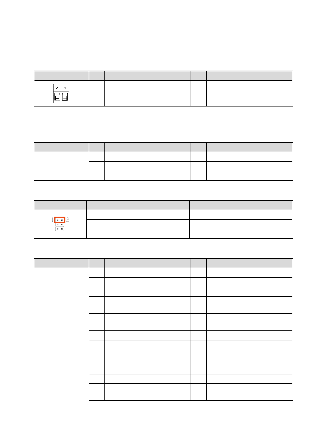
7.1
D
C Power Input 24V: Terminal Block, 2*1P, 3.50mm (Mark No.3, DC_IN2)
Graphic Pin Definition Pin Definition
1 GND 2 VCC_IN
[1]
Notes:
[1]: DC Power Input can be 24V/12V, selectable by BOM.
eDP/LVDS Backlight Control: Wafer, 6*1P,
7.2
2.
00mm (Mark No.7, LVDS_P1)
Graphic Pin Definition Pin Definition
1 GND 4 BKLT_EN
2 GND 5 VCC12S
3 BKLT_CTL 6 VCC12S
LVDS VDD Select: Jumper,3*2P, 2.54mm (M
7.3
ark
No.8, JV_LVDS1)
Graphic Setting Function
1-2(Default) VCC3.3
3-4 VCC5
5-6 VCC12
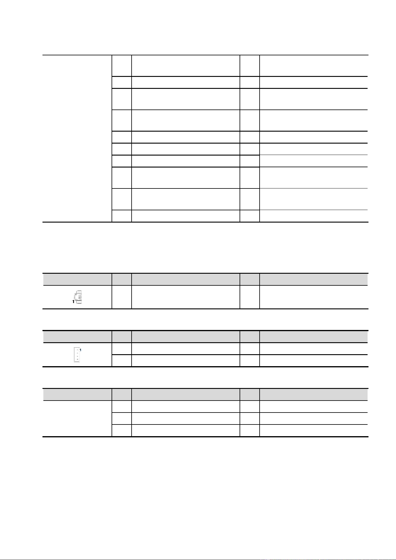
eDP/LVDS Signal: Wafer, 20*2P, 1.25mm (M
7.4
ark
No.9, LVDS1)
Graphic Pin Definition Pin Definition
1 VDD_PANEL
[1]
2 VDD_PANEL
[1]
3 LVDS_PRSNT 4 GND
5 VDD_PANEL
[1]
6 VDD_PANEL
[1]
7 LVDS_A_DATA0- 8
LVDS_B_DATA0-
/EDP1_TX0-
[2]
9 LVDS_A_DATA0+ 10
LVDS_B_DATA0+
/EDP1_TX0+
[2]
11
GND
12 GND
13 LVDS_A_DATA1- 14
LVDS_B_DATA1-
/EDP1_TX1-
[2]
15 LVDS_A_DATA1+ 16
LVDS_B_DATA1+
/EDP1_TX1+
[2]
17 GND 18 GND
19 LVDS_A_DATA2- 20
LVDS_B_DATA2-
/EDP1_AUX-
19
21 LVDS_A_DATA2+ 22
LVDS_B_DATA2+
/EDP1_AUX+
23 GND 24 GND
25 LVDS_A_CLK- 26
LVDS_B_CLK-
/EDP1_TX3-
[2]
27 LVDS_A_CLK+ 28
LVDS_B_CLK+
/EDP1_TX3+
[2]
29 GND 30 GND
31 N/C 32 EDP1_HPD_C
33 GND 34 GND
35 LVDS_A_DATA3- 36
LVDS_B_DATA3-
/EDP1_TX2-
[2]
37 LVDS_A_DATA3+ 38
LVDS_B_DATA3+
/EDP1_TX2+
[2]
39 N/C 40 GND
Notes:
[1]: Panel Power VDD is 3.3V by default, 5V or 12V is selectable by “eDP/LVDS VDD Select Jumper”. (JV_LVDS1, Mark 8).
[2]: It supports LVDS by default and can support eDP if specified. (BOM selectable).
Amplifier: Wafer, 2*1P, 1.25mm (M
7.5
ark
No.10, J_SPK1)
Graphic Pin Definition Pin Definition
1 VCC_BAT 2 GND
SATA Power: Wafer, 4*1P, 2.00mm (Mark No.12,
7.6
P
_SATA1)
Graphic Pin Definition Pin Definition
1 VCC12 3 GND
2 GND 4 VCC5
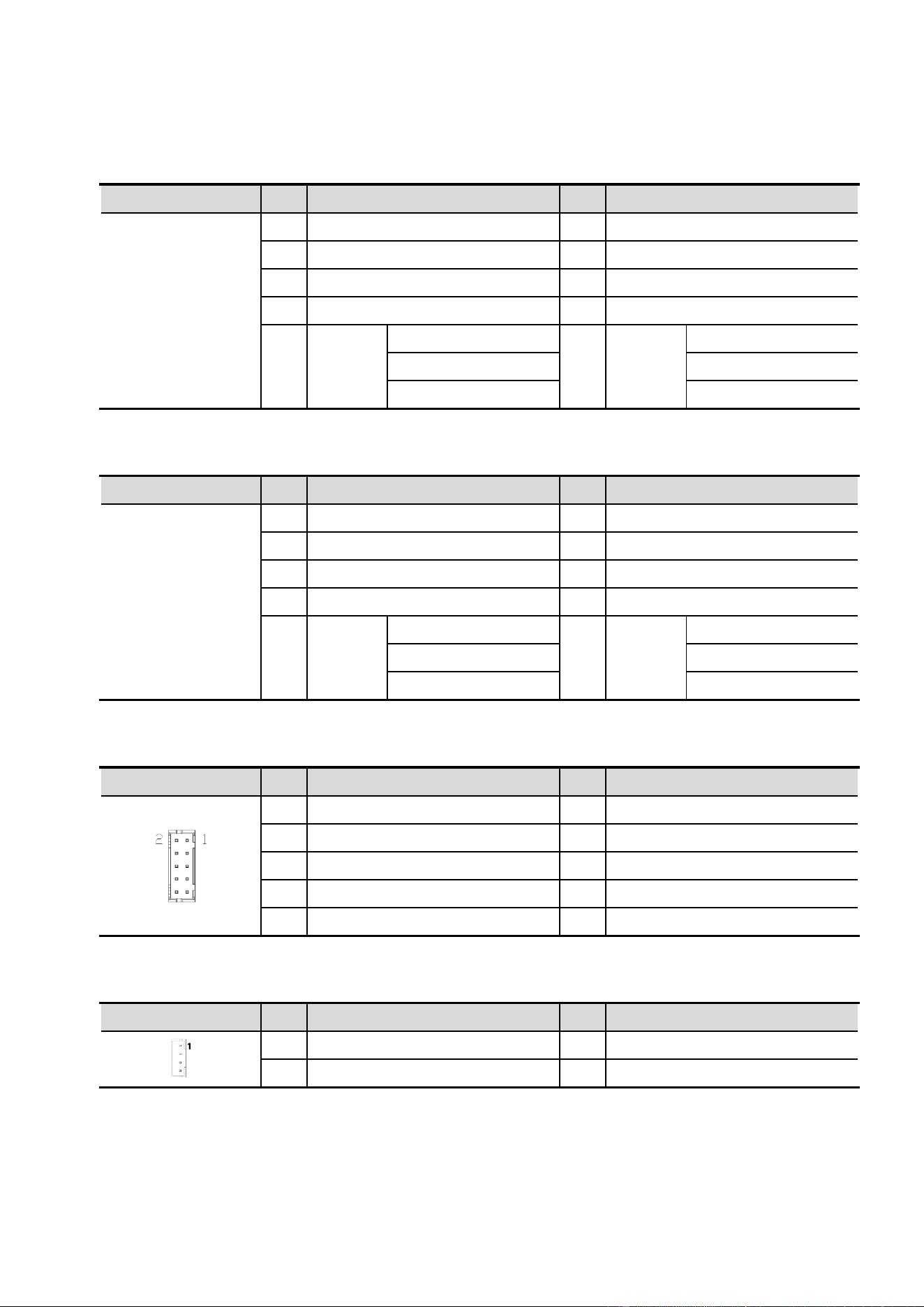
SIM Card: Wafer, 6*1P, 1.25mm (M
7.7
ark
No.16, J_SIM1)
Graphic Pin Definition Pin Definition
1 UIM_PWR 4 UIM_CLK
2 UIM_DATA 5 UIM_RST
3 GND 6 UIM_VPP
20
GbE LAN: RJ45 Connector (M
7.8
ark
No.17, LAN1)
Graphic Pin Definition Pin Definition
1 MDI0+ 5 MDI2-
2 MDI0- 6 MDI1-
3 MDI1+ 7 MDI3+
4 MDI2+ 8 MDI3-
A
Active
LED
ACT: Twinkling Green
B
Speed
LED
1000M: Turn Yellow
Only LINK: Lights Off 100M: Turn Green
Stop: Lights Off 10M: Lights Off
GbE LAN: RJ45 Connector (M
7.9
ark
No.18, LAN2)
Graphic Pin Definition Pin Definition
1 MDI0+ 5 MDI2-
2 MDI0- 6 MDI1-
3 MDI1+ 7 MDI3+
4 MDI2+ 8 MDI3-
A
Active
LED
ACT: Twinkling Green
B
Speed
LED
1000M: Turn Yellow
Only LINK: Lights Off 100M: Turn Green
Stop: Lights Off 10M: Lights Off
Front USB2.0: Wafer, 5*2P, 2.00mm (M
7.10
ark
No.22, F_USB1)
Graphic Pin Definition Pin Definition
1 VCC5 2 VCC5
3 USB2.0_1- 4 USB2.0_2-
5 USB2.0_1+ 6 USB2.0_2+
7 GND 8 GND
9 GND 10 GND
Front USB2.0: Wafer, 4*1P, 2.00mm (Mark No.23, F_USB2
7.11
)
Graphic Pin Definition Pin Definition
1 VCC5 3 USB2.0+
2 USB2.0- 4 GND
21
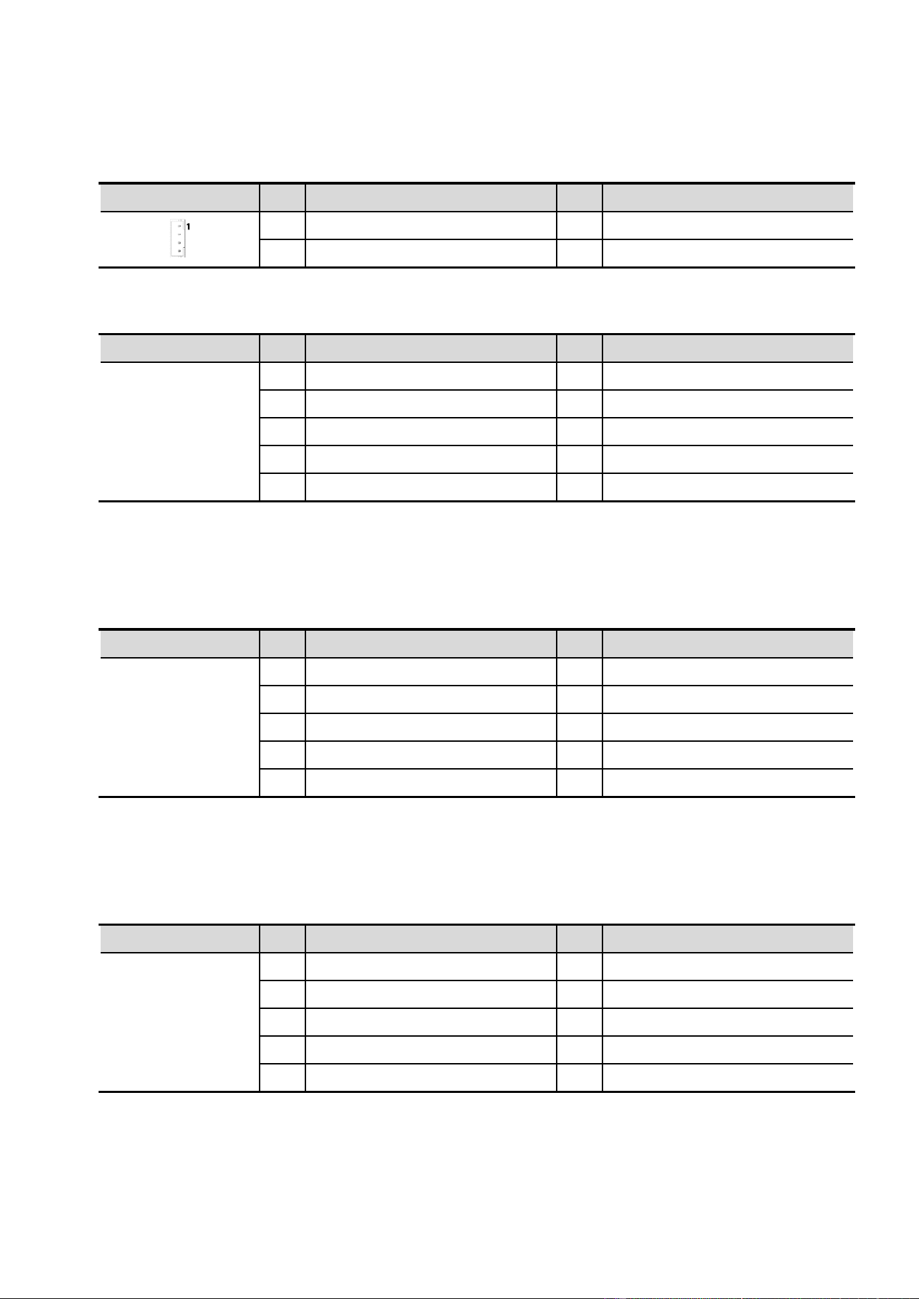
Front USB2.0: Wafer, 4*1P, 2.00mm (Mark No.24, F_USB3
7.12
)
Graphic Pin Definition Pin Definition
1 VCC5 3 USB2.0+
2 USB2.0- 4 GND
COM1: Wafer, 9*1P, 1.25mm (M
7.13
ark
No.25, J_COM1)
Graphic Pin Definition Pin Definition
1 PIN1
[1]
6 CTS
2 DSR 7 DTR
3 RXD 8 PIN9
[2]
4 RTS 9 GND
5 TXD
Notes:
[1]: PIN1 can be DCD#/5V selectable by RES, support DCD# by default.
[2]: PIN9 can be RI#/12V selectable by RES, support RI# by default.
COM2: Wafer, 9*1P, 1.25mm (M
7.14
ark
No.26, J_COM2)
Graphic Pin Definition Pin Definition
1 PIN1
[1]
6 TXD
2 RXD 7 RTS
3 DSR 8 PIN9
[2]
4 DCD 9 GND
5 DTR
Notes:
[1]: PIN1 can be CTS#/5V selectable by RES, support DCD# by default.
[2]: PIN9 can be RI#/12V selectable by RES, support RI# by default.
COM3: Wafer, 9*1P, 1.25mm (M
7.15
ark
No.27, J_COM3)
Graphic Pin Definition Pin Definition
1 PIN1
[1]
6 TXD
2 RXD 7 RTS
3 DSR 8 PIN9
[2]
4 DCD 9 GND
5 DTR
Notes:
[1]: PIN1 can be CTS#/5V SEL by selectable, support DCD# by default.
[2]: PIN9 can be RI#/12V SEL by selectable, support RI# by default.
22
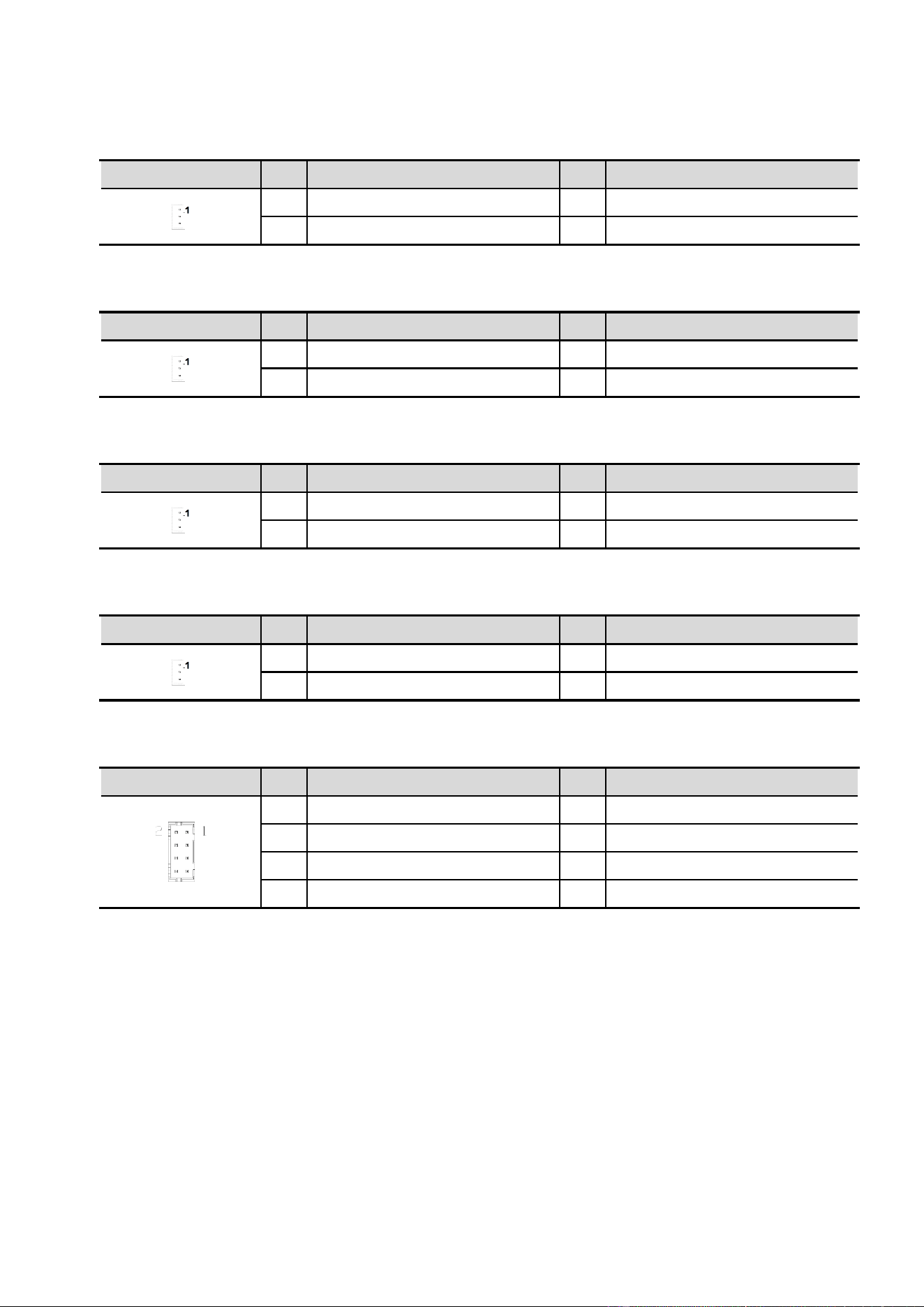
COM4: Wafer, 3*1P, 2.00mm (M
7.16
ark
No.28, J_COM4)
Graphic Pin Definition Pin Definition
1 RXD 3 GND
2 TXD
COM5: Wafer, 3*1P, 2.00mm (M
7.17
ark
No.29, J_COM5)
Graphic Pin Definition Pin Definition
1 RXD 3 GND
2 TXD
COM6 RS485: Wafer, 3*1P, 2.00mm (M
7.18
ark
No.30, J_COM6_RS1)
Graphic Pin Definition Pin Definition
1 RS485+ 3 GND
2 RS485-
COM6: Wafer, 3*1P, 2.00mm (M
7.19
ark
No.31, J_COM6)
Graphic Pin Definition Pin Definition
1 RXD 3 GND
2 TXD
Front Panel: Wafer, 4*2P, 2.00mm (Mark No.32, F_PANEL1
7.20
)
Graphic Pin Definition Pin Definition
1 PWR LED+ 2 HDD_LED+
3 PWR LED- 4 HDD_LED-
5 PWR On+ 6 RESET-
7 PWR On- 8 RESET+
23
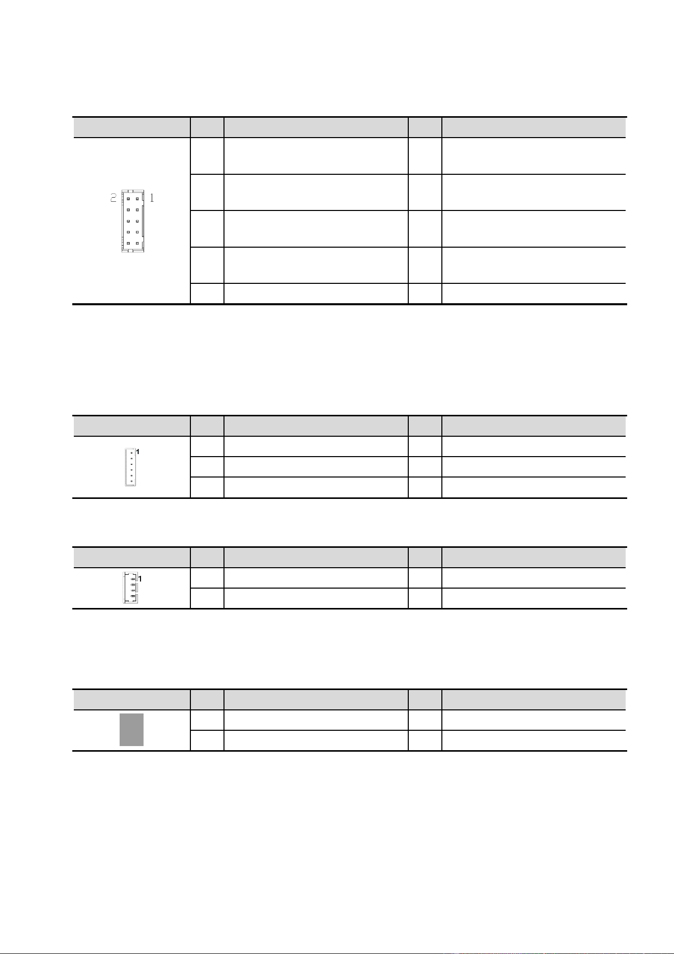
GPIO: Wafer, 5*2P, 2.00mm (Mark No.33, J_GPIO1
7.21
)
Graphic Pin Definition Pin Definition
1
SIO_GPI71
(0xA06 Bit1, H
[1]
)
2
SIO_GPI70
(0xA06 Bit0, H
[1]
)
3
SIO_GPI73
(0xA06 Bit3, H
[1]
)
4
SIO_GPI72
(0xA06 Bit2, H
[1]
)
5
SIO_GPO75
(0xA06 Bit5, H
[1]
)
6
SIO_GPO74
(0xA06 Bit4, H
[1]
)
7
SIO_GPO77
(0xA06 Bit7, H
[1]
)
8
SIO_GPO76
(0xA06 Bit6, H
[1]
)
9 GND 10 +3.3V
[2]
Notes:
[1]: “H” or “L” means the default voltage is High or Low level (3.3V GPIO).
[2]: Power on this Pin is 3.3V by default, 5V is available if specified. (resistor selectable)
I2C: Wafer, 6*1P, 1.25mm (Mark No.34, J_I2C1
7.22
)
Graphic Pin Definition Pin Definition
1 VCC3.3 4 RST
2 GND 5 SCL
3 INT 6 SDA
CPU FAN: Wafer, 4*1P, 1.25mm (Mark No.35, CPU_FAN1
7.23
)
Graphic Pin Definition Pin Definition
1 GND 3 FAN Speed Detection
2 VCC12
[1]
4 FAN Speed Control
Notes:
[1]: Power on this Pin is 12V by default,5V is available if specified. (resistor selectable)
Power Debug: Wafer, 4*1P, 1.25mm (Mark No.36, J_PRM1
7.24
)
Graphic Pin Definition Pin Definition
1 GND 3 VCCIN_SCL
2 VCCIN_PE 4 VCCIN_SDA
24
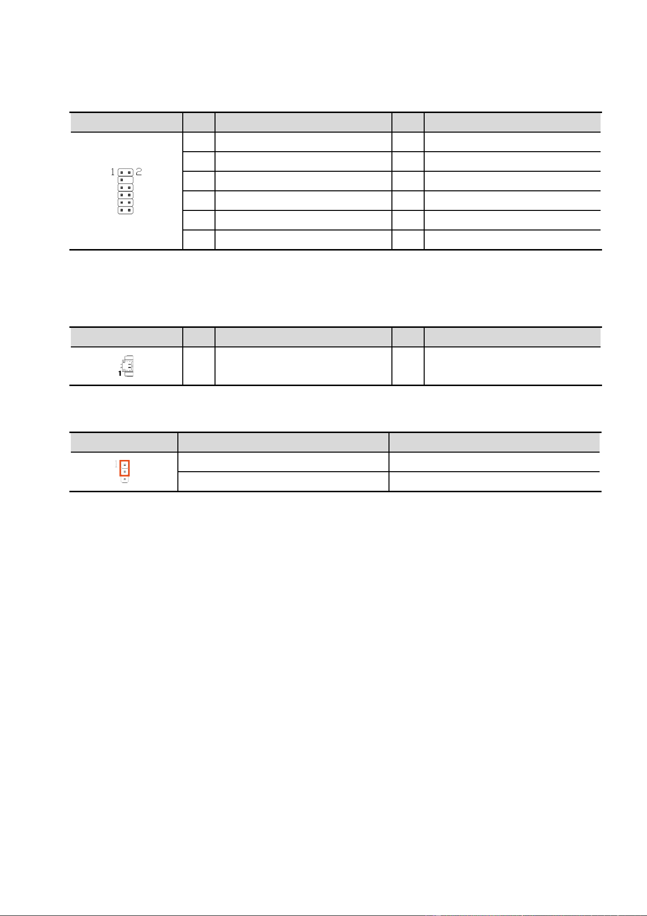
ESPI Debug: Header, 6*2P, 2.00mm (Mark No.37, J_ESPI1
7.25
)
Graphic Pin Definition Pin Definition
1 ESPI_IO0 2 VCC3.3
3 ESPI_IO1
5 ESPI_IO2 6 ESPI_CLK
7 ESPI_IO3 8 GND
9 ESPI_CS0- 10 VCC3.3
11 ESPI_ALERT0_N 12 PLTRST_N
[1]
Notes:
[1]: Signal on this Pin is PLT_RST_N by default, ESPI_RST0_N is available if specified. (resistor selectable).
CMOS Battery: Wafer, 2*1P, 1.25mm (Mark No.38, J_BAT1
7.26
)
Graphic Pin Definition Pin Definition
1 VCC_BAT 2 GND
CMOS Clear: Jumper,3*1P, 2.54mm (Mark No.39
7.27
,
CLR_CMOS1)
Graphic Setting Function
1-2(Default) Normal
2-3 Clear CMOS
25

8 BIOS Setup
Notice! The BIOS options in this manual are for reference only. Different
configurations may lead to difference in BIOS screen and BIOS
screens in manuals are usually the first BIOS version when the board
is released and may be different from your purchased motherboard.
Users are welcome to download the latest BIOS version form our
official website.
The BIOS is a program located on a Flash Memory on the motherboard. This
program is a bridge between motherboard and operating system. When you start
the computer, the BIOS program will gain control. The BIOS first operates
an auto-diagnostic test called POST (power on self test) for all the
necessary hardware, it detects the entire hardware device and configures the
parameters of the hardware synchronization. Only when these tasks are
Power on the computer and by pressing <Del> immediately allows you to
enter Setup.
If the message disappears before your respond and you still wish to enter Setup,
restart the system to try again by turning it OFF then ON or pressing the
“RESET” button on the system case. You may also restart by simultaneousl
completed done it gives up control of the computer to operating system (OS).
Since the BIOS is the only channel for hardware and software to communicate,
it is the key factor for system stability, and in ensuring that your system
performance as its best.
8.1 Entering Setup
y
pressing <Ctrl>, <Alt> and <Delete> keys. If you do not press the keys at the
correct time and the system does not boot, an error message will be displayed
and you will again be asked to
Press <Del> to enter S
etup; press < F7> to enter pop-up Boot menu.
BIOS Boot Menu Screen (boot device options please refer to actual configuration)
26

The following diagram show a general BIOS menu screen
8.2 BIOS Menu Screen
:
Menu Bar
In the above BIOS Setup main menu of, you can see several options. W
8.3 Function Keys
e
will explain these options step by step in the following pages of this chapter,
but let us first see a short description of the function keys you may use here:
Press←→ (left, right) to select screen.
Press ↑↓ (up, down) to choose, in the main menu, the option you want to
confirm or to modify.
Press <Enter> to select.
Press <+>/<-> keys when you wa
nt to modify the BIOS parameters for the
active option.
[F1]: General help.
[F2]: Previous values.
[F3]: Optimized defaults.
[F4]: Save & Exit.
Main Men
Press <Esc> to exit from BIOS Setup.
8.4 Getting Help
u
The on-line description of the highlighted setup function is displayed at the top
right corner the screen.
↓
General Help Items
Current Setting Value
Menu Items
Function Keys
27

There are six menu bars on top of BIOS screen
Status Page Setup Menu/Option Page Setup Menu
Press 【F1】 to pop up a small help window that describes the appropriate keys
to use and the possible selections for the highlighted item. To exit the Help
Window, press <Esc>.
8.5 Menu Bars
:
Main To change system basic configuration
Advanced To change system advanced configuration
Chipset To change chipset configuration
Security Password settings
Boot To change boot settings
Save & Exit Save setting, loading and exit options.
Main menu screen includes some basic system information. Highlight the ite
User can press the right or left arrow key on the keyboard to switch from menu
bar. The selected one is highlighted.
8.6 Main Menu
m
and then use the <+> or <-> and numerical keyboard keys to select the value you
want in each item.
System Date
Set the date. Please use [Tab] to switch between date elements.
System Time
Set the time. Please use [Tab] to switch between time elements.
28

8.7 Advanced Menu
CPU Configuration
Press [Enter] to view current CPU configuration and make settings for the
following sub-items:
Efficient-Core Information
Use this item to displays the E-Core information.
Press [Enter] to make settings for the following sub-items:
Intel VMX Virtualization Technology
:
When enabled
,
a VMM can utilize the additional hardware capabilities provided
by Vanderpool Technology.Set the default value to: [Enabled].The optional
settings: [Enabled]; [Disabled].
C States
:
Use this item to enable/disable CPU Power Management.Allows CPU to go to C
states when it’s not 100% utilized.Set the default value to: [Enabled].The optional
settings: [Enabled]; [Disabled].
Turbo Mode
:
Use this item to enable/disable processor Turbo Mode(requires EMTTM enabled
too).AUTO means enabled.Set the default value to: [Enabled].The optional settings:
[Enabled]; [Disabled].
View/Configure Turbo Options
:
Use this item to View/Configure Turbo Options
Performance-Core Information
Boot Performance Mode
Use this item to select the performance state that the BIOS will set starting from
reset vertor.
Boot Performance Mode Set the default value to: [Turbo Performance].
The optional settings: [Min Non-Turbo Performance]; [Max Non-Turbo
Performance]; [Turbo Performance].
29

PCH-FW Configuration
Use this item to Configure Management Engine Technology Paramenters.
Trusted Computing
Press [Enter] to view current status information, or make further settings in the
following sub-items:
Security Device Support
Use this item to enable or disable BIOS support for security device. O.S. will not
show Security Device. TCG EFI protocol and INT1A interface will not be
available.
Security Device Support Set the default value to: [Enabled].
The optional settings: [Disabled]; [Enabled].
When set as [Enabled], user can make further settings
in the following items:
Active PCR Banks
Available PCR Banks
SHA256 PCR Bank
Use this item to Enable or Disable SHA256 PCR Bank
SHA256 PCR Bank Set the default value to: [Enabled].
The optional settings: [Disabled]; [Enabled].
SHA384 PCR Bank
Use this item to Enable or Disable SHA384 PCR Bank
SHA384 PCR Bank Set the default value to: [Disabled].
The optional settings: [Disabled]; [Enabled].
Pending Operation
Use this item to schedule an operation for the security device
NOTE: Your computer will reboot during restart in order to change state of
security device
Pending Operation Set the default value to: [None].
The optional settings: [None]; [TPM Clear].
Physical Presence Spec Version
Use this item to select to Tell O.S. to support PPI Spec Version 1.2 or 1.3. Note
some HCK tests might not support 1.3. Set the default value to: [1.3]. The
optional settings: [1.3]; [1.2].
Device Select
TPM 1.2 will restrict support to TPM 1.2 devices,TPM 2.0 will restrict support to
TPM 2.0 devices,Auto will support both with the default set to TPM 2.0 devices if
not found,TPM 1.2 devices will be enumerated. Set the default value to: [Auto].
optional settings: [TPM 1.2]; [TPM 2.0]; [Auto].
ACPI Settings
Press [Enter] to make settings for the following sub-item:
ACPI Sleep State
Use this item to select the highest ACPI sleep state the system will enter when
the SUSPEND button is pressed.
Pending Operation Set the default value to: [S3(Suspend to RAM)]
The optional settings: [Suspend Disabled]; [S3(Suspend to RAM)].
Super I/O Configuration
Press [Enter] to make settings for the following sub-item:
Super IO Configuration
Serial Port 1 Configuration
Use this item to set parameters of serial port 1 (COMA)
Press [Enter] to make settings for the following sub-item:
30

Serial Port
Use this item to enable or disable serial port (COM)
Pending Operation Set the default value to: [Enabled].
The optional settings: [Disabled]; [Enabled].
When set as [Enabled], user can make further settings in the following items:
Device Settings
Change Settings
Use this item to select an optimal settings for super IO device
Change Settings Set the default value to: [Auto]
The optional settings: [Auto]; [IO= 3F8h; IRQ=4]; [IO= 2F8h; IRQ=3].
PC Health Status
Press [Enter] to view current hardware health status, make further settings in
‘SmartFAN Configuration’ and set value in ‘Shutdown Temperature’.
Power Control
Press [Enter] to make settings for the following sub-items:
Power On after Power Failure
Use this item to specify what state to go to when power is re-applied after a power
failure.
System State after Power Failure Set the default value to: [Power off].
The optional settings: [Power On]; [Power off]; [Last State].
Soft Off by PWR-BTTN
Use this item to s e t s o f t off mode. Set the default value to: [Instant Off]. The
optional settings: [Instant Off]]; [Delay 4 Sec].
Power Limit 4 Override
Use this item to enabled/disable power Limit 4 override. If this option is disabled,
BIOS will program the default values for Power Limit 4.
Power Limit 4 Override Set the default value to: [Enabled].
The optional settings: [Disabled]; [Enabled].
When set as [Enabled], user can make further settings in the following items:
Power Limit 4
Use this item to power Limit 4 vallue in Milli watts. BIOS will round to the nearest
1/8W when programming. If the value is 0, BIOS will program this value as
1.25*TDP. For 12.50W, enter 12500. Processor applies control policies such that
the package power does not exceed this limit.
Power Limit 4 Set the default value to: [0].
When set as [Enabled], the following items shall appear:
USB Configuration
Press [Enter] to make settings for the following sub-items:
USB Configuration
XHCI Hand-off
This is a workaround for OSes without XHCI hand-off support. The XHCI
ownership change should be claimed by XHCI driver.
XHCI Hand-off Set the default value to: [Enabled].
The optional settings: [Enabled]; [Disabled].
USB Mass Storage Driver Support
Use this item to enable or disable USB mass storage driver support.
USB Mass Storage Driver Support Set the default value to: [Enabled].
The optional settings: [Disabled]; [Enabled].
USB hardware delays and t
ime-outs:
31

USB transfer time-out
Use this item to set the time-out value for Control, Bulk, and Interrupt transfers.
USB transfer time-out Set the default value to: [20 sec].
The optional settings: [1 sec]; [5 sec]; [10 sec]; [20 sec].
Device Reset time-out
Use this item to set USB mass storage device Start Unit command time-out.
Device Reset time-out Set the default value to: [20 sec].
The optional settings: [10 sec]; [20 sec]; [30 sec]; [40 sec].
Device Power-up delay
Use this item to s
et maximum time the device will take before it properly reports
itself to the host controller. ‘Auto’ uses default value: for a root port it is 100 ms, for
a hub port the delay is taken from hub descriptor.
Device Power-up delay Set the default value to: [Auto].
The optional settings: [Auto]; [Manual].
When set as [Manual], user can make further settings in the following items:
Device Power-up Delay in Seconds
Use this item to delay range is 1..40 seconds, in one second increments
Device Power-up Delay in Seconds Set the default value to: [5].
Network Stack Configuration
Press [Enter] to go to ‘Network Stack’ screen to make further settings.
Network Stack
Use this item to enable or disable UEFI Network Stack.
Network Stack Set the default value to: [Disabled]
The optional settings: [Disabled]; [Enabled].
When set as [Enabled], the following sub-items shall appear:
IPv4 PXE Support
Use this item to enable IPv4 PXE boot support. When set as [Disabled], IPv4 boot
support will not be available.
IPv4 PXE Support Se
t the default value to: [Enabled].
The optional settings: [Disabled]; [Enabled].
IPv6 PXE Support
Use this item to enable IPv6 PXE boot support. When set as [Disabled], IPv6 boot
support will not be available.
IPv6 PXE Support Set the default value to: [Disabled].
The optional settings: [Disabled]; [Enabled].
PXE Boot Wait Time
Use this item to set wait time to press [ESC] key to abort the PXE boot.
Use either [+] / [-] or numeric keys to set the value.
PXE Boot Wait Time Set the default value to: 5
Media Detect Count
Use this item to set number of times presence of media will be checked.
Use either [+] / [-] or numeric keys to set the value.
Media Detect Count Set the default value to: 5
NVMe Configuration
Press [Enter] to view current NVMe Configuration.
*Note: options only when NVME device is available.
32

8.8 Chipset Menu
System Agent (SA) Configuration
Press [Enter] to make settings for the following sub-items:
Memory Configuration
Use this item to Search for memory parameter information.
PCH-IO Configuration
Press [Enter] to make settings for the following sub-items:
PCH-IO Configuration
SATA Configuration
Press [Enter] to make settings for the following sub-items:
SATA Controller(s)
Use this item to enable or disable SATA device.
SATA Controller Set the default value to: [Enabled].
The optional settings: [Disabled]; [Enabled].
When set as [Enabled], the following sub-items shall appear:
M.2
Port
Port
Port Set the default value to: [Enabled].
The optional settings: [Disabled]; [Enabled].
SATA Port
Port
Port Set the default value to: [Enabled].
The optional settings: [Disabled]; [Enabled].
USB Configuration
USB Port Disable Override
Selectively Enable/Disable the corresponding USB port from reporting a Device
Connection to the controller. Set the default value to: [Disabled].
The optional settings: [Disabled]; [Enabled].
33

I2C Touch Panel
Indicates what type of I2C Touch Panel is connected to this Serial IO controller. Set
the default value to: [Disabled].
The optional settings: [Disabled]; [Enabled].
8.9 Security Menu
Security menu allow users to change administrator password and user password
settings.
Administrator Password
If there is no password present on system, please press [Enter] to create new
administrator password. If password is present on system, please press [Enter] to
verify old password then to clear/change password. Press again to confirm the
new administrator password.
User Password
If there is no password present on system, please press [Enter] to create new
use
r password. If password is present on system, please press [Enter] to verify
old password then to clear/change password. Press again to confirm the new
administrator password.
Secure Boot
Press [Enter] to make customized secure settings:
System Mode
Secure Boot
Secure Boot feature is active if secure boot is enabled, Platform Key(PK) is
enrolled and the system is in user mode. The mode change requires platform
reset.
34

Boot Configuration
Setup Prompt Timeout
Use this item to set number of seconds to wait for setup activation key.
65535(0Xffff) means indefinite waiting
Setup Prompt Timeout Set the default value to: [1].
Bootup Numlock State
Use this item to select keyboard numlock state.
Bootup Numlock State Set the default value to: [Off].
The optional settings are: [On]; [Off].
FullScreen Logo
Use this item to enable or disables FullScreen Logo
option. Set the default value to: [Disabled].
The optional settings are: [Disabled]; [Enabled].
Boot Option Priorities
Boot Option #1
Boot Option #1 Set the default value to: [UEFI: Built-in EFI Shell]
The optional settings are: [UEFI: Built-in EFI Shell]; [Disabled
Secure Boot Set the default value to: [Enabled].
The optional settings are: [Disabled]; [Enabled].
8.10 Boot Menu
.
35

8.11 Save & Exit Menu
Save Changes and Reset
This item allows user to reset the system after saving the changes.
Discard Changes and Reset
This item allows user to reset the system without saving any changes.
Restore Defaults
Use this item to restore /load default values for all the setup options.
Save as User Defaults
Use this item to save the changes done so far as user defaults.
Restore User Defaults
Use this item to restore defaults to all the setup options.
Boot Override
UEFI: Built-in EFI Shell
9Driver Installation
First, users need to download the driver compatible with their motherboard and operating
system version from the official website of Dongtian to this device. Make sure to download the latest
version of the driver for the best performance and compatibility. The download address can be
found at http://dtipcshop.com/
9.1 Download Driver:
.
36

Once the download is complete, extract the driver files to an easily accessible folder
9.2 Unzip the file:
.
Find the setup program (usually an .exe file) in the unzipped folder and double-click it to run it.
Follow the prompts to complete the installation process, which usually requires you to agree to the
license agreement and select the installation path
9.3 Run the installer:
.
37

38

After installation, some drivers may require you to restart your computer to take effect
9.4 Restart your computer:
.
After the installation is complete, you can use the Device Manager to verify whether the driver
has been successfully installed
9.5 Check the driver:
.
39

10Network and WiFi connections
[Network connected]
In the device command prompt, enter a URL to check whether the network is connecte
10.1 Network connection:
You can check whether the network icon in the lower right corner of the device prompts
d
successfully. Usually, a successful connection will show no packet loss.
40

You can check whether the WIFI icon in the lower right corner of the device prompts [WIFI is
available
10.2 WiFi connection:
]
You can check whether the WIFI module is recognized by the device manager.
In the device command prompt, enter a URL to check whether the WIFI connection is successful.
Usually, if the connection is successful, it will show no packet loss.
If it cannot be recognized, it is recommended to restart the device and try again.
41

FCC Warning
This device complies with part 15 of the FCC rules. Operation is subject to the following two
conditions: (1) this device may not cause harmful interference, and (2) this device must accept any
inte rference received, including interference that may cause undesired operation.
Changes or modifications not expressly approved by the party responsible for compliance could void
the user's authority to operate the equipment.
NOTE: This equipment has been tested and found to comply with the limits for a Class B digital
device, pursuant to part 15 of the FCC Rules. These limits are designed to provide reasonable
protection against harmful interference in a residential installation. This equipment generates uses
and can radiate radio frequency energy and, if not installed and used in accordance with the
instructions, may cause harmful interference to radio communications. However, there is no
guarantee that interference will not occur in a particular installation. If this equipment does cause
harmful interferenceto radio or television reception, which can be determined by turning the
equipment off and on, the user is encouraged to try to correct the interference by one or more of the
following measures:
-Reorient or relocate the receiving antenna.
•Increase the separation between the equipment and receiver.
•Connect the equipment into an outlet on a circuit different from that to which the receiver is
connected.
•Consult the dealer or an experienced radio/TV technician for help.
Radiation Exposure Statement
This equipment complies with FCC radiation exposure limits set forth for an uncontrolled
environment. This equipment should be installed and operated with minimum distance 20cm between
the radiator and your body.