SPECIFICATION
SFX Form Factor
SST-ST45SF
450W Switching Power Supply
Active PFC Circuit
Full Range Input
01
This is the specification of Model SST-ST45SF; AC-line powered switching power
supply with active PFC (Power Factor Correction) circuit, meet EN61000-3-2 and
with Full Range Input features.
The specification below is intended to describe as detailedly as possible the functions
and performance of the subject power supply. Any comment or additional requirements
to this specification from our customers will be highly appreciated and treated as a new
target for us to approach.
The subject power supply will meet the EMI requirements and obtain main safety
approvals
as following:
2.1. EMI REGULATORY
- FCC Part 15 Subpart J, Class ‘B’ 115 Vac operation.
- CISPR 22 Class ‘B’ 230 Vac operation.
1.GENERAL DESCRIPTION AND SCOPE
2. REFERENCE DOCUMENTS
02
3. INPUT ELECTRICAL SPECIFICATIONS
3.1. AC INPUT
ParameterParameter
Min.
Nom.
Max
Unit
Maximum inrush current from power-on (with power on at any point on the AC sine)
and including, but not limited to, three line cycles, shall be limited to a level below the
surge rating of the input line cord, AC switch if present, bridge rectifier, fuse, and EMI
filter components. Repetitive ON/OFF cycling of the AC input voltage should not
damage the power supply or cause the input fuse to blow.
(At Full load)
3.2. INRUSH CURRENT
3.3. INPUT LINE CURRENT & POWER FACTOR (P.F.)
3.4. EFFICIENCY
(1)
Vin (115VAC) 90 115 135 VAC rms
Vin (230VAC) 180 230 265 VAC rms
Vin Frequency 47 -- 63 HZ
AC input
Input line current
P.F.@ Full Load
P.F.@ Pin=75W
115V < 5.5Amps – rms > 0.95 > 0.8
230V
Loading
Required Minimum Efficiency
Required Minimum Efficiency
< 3Amps – rms
> 0.9
Voltage
115V
230V
Full load
>82%
>84%
>82%
>84%
Typical load
>85%
>87%
Light load
> 0.65
Nominal voltages for test purposes are considered to be within ±1.0V of nominal.
Minimum Efficiency for test purposes are considered to be within ±1.0% of nominal.
SFX Form Factor
03
( 1 ) +3.3V & 5V total output not exceed 120W.
( 2 )Total output continuous shall not exceed 450W watts.
( 3 )5Vsb Peak current is 3A(less then 500m Sec.), minimum voltage during peak is
> 4.5Vdc. Voltages and ripple are measured at the load side of mating connectors
with a 0.1 uF monolithic ceramic capacitor paralleled by a 10 uF electrolytic capacitor
across the measuring terminals.
The cross regulation defined as follows, the voltage regulation limits DC include DC
Output ripple & noise.
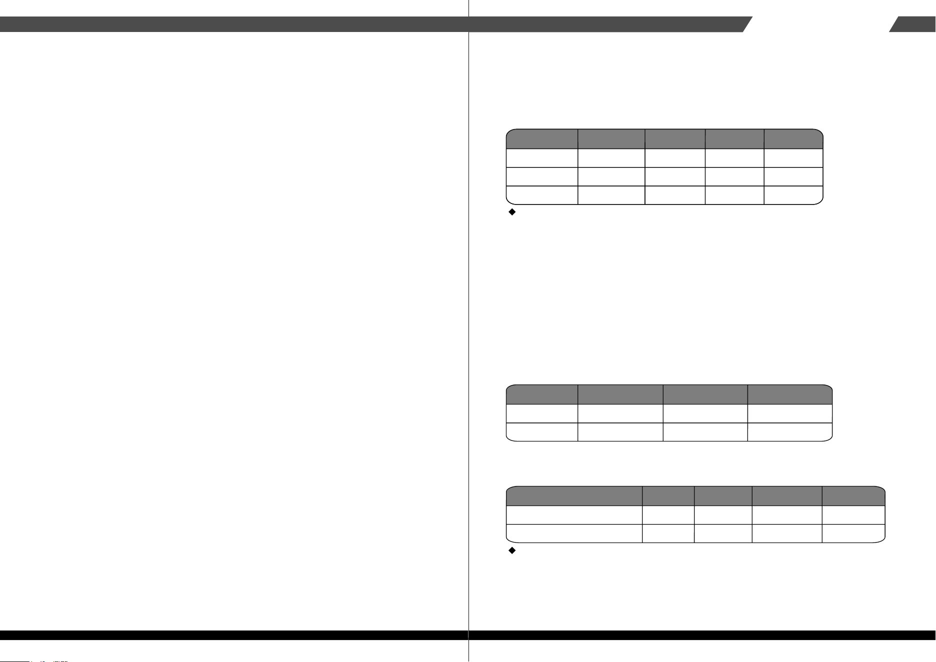
4.1. OUTPUT VOLTAGE AND CURRENT RATING
4.2. LOAD CAPACITY SPECIFICATIONS
4 . OUTPUT ELECTRICAL REQUIREMENTS
Output
+3.3V
+5V
+12V
-12V
+5VSB
MINIMUM
LOAD
0.1A
0.2A
0.6A
0A
0A
NORMAL
LOAD
10.5A
11A
18A
0.25A
1.25A
MAXIMUM
LOAD
PEAK
LOAD
LOAD
REG
21A
22A
36A
0.5A
2.5A
MAXIMUM
LOAD
70mV P-P
70mV P-P
140mV P-P
140mV P-P
70mV P-P
±5%
±5%
±5%
±10%
±5%
LINE
REG
±1%
±1%
±1%
±1%
±1%3A
LOAD +3.3V +5V +12V -12V +5VSB
Condition_1 X X X X 2.5A
Condition_2 0.1A 0.2A 0.6A 0A 0A
Condition_3 0.1A 0.2A 0.6A 0.5A 0A
Condition_4 1A 10A 18A 0.1A 0.1A
Condition_5 2A 2A 36A 0.1A 0.1A
Condition_6 1A 14A 2A 0.1A 0.1A
Condition_7 3A 22A 26A 0.5A 1.5A
Condition_8 18A 2A 2A 0A 0.1A
Condition_9 21A 10A 26A 0.5A 1.5A
04
STRIDER ST1000STRIDER ST1000-NV
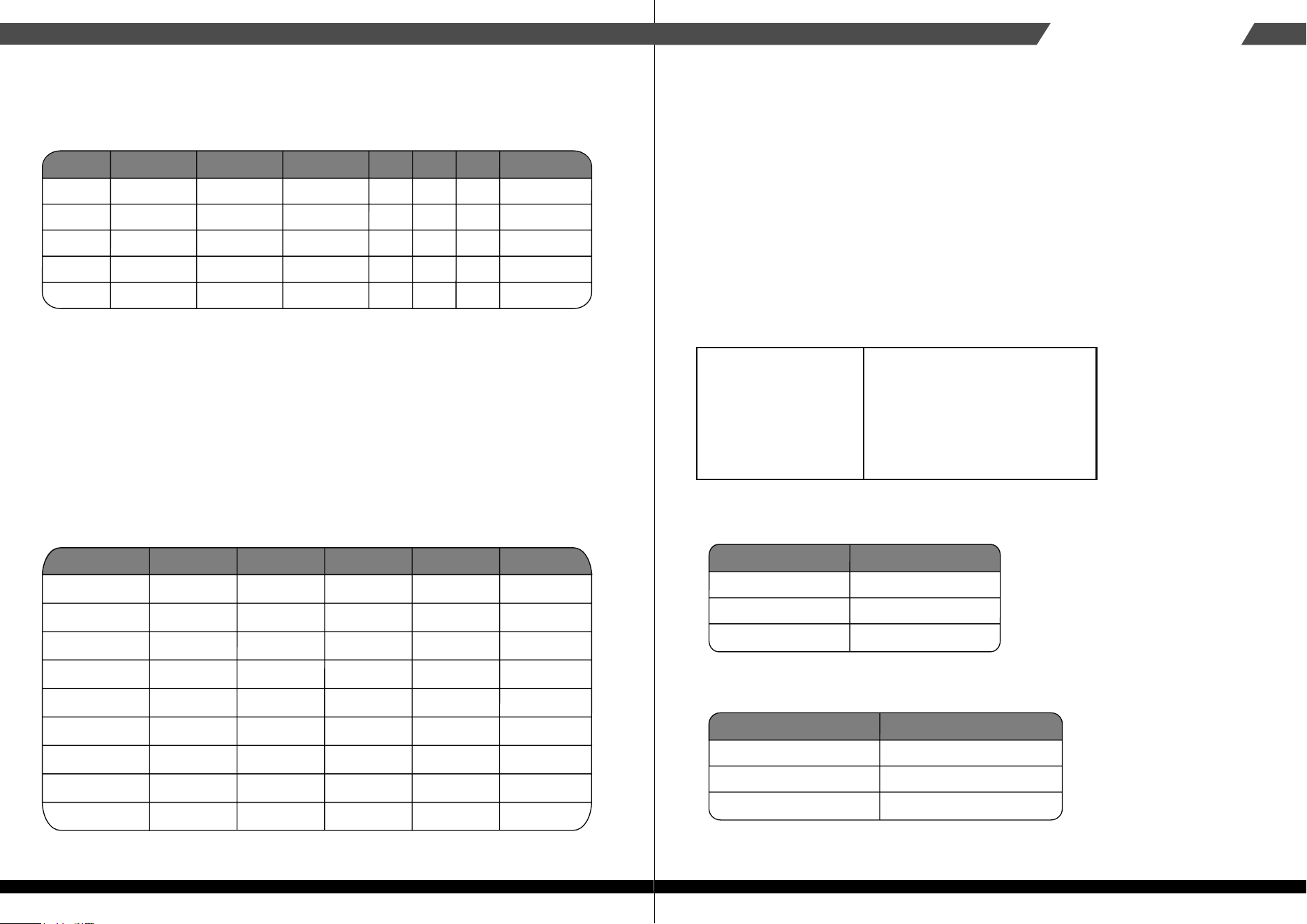
4.3. HOLD-UP TIME (@Typical Load of Table. 1)
115V / 60Hz : 17 m Sec. Minimum.
230V / 50Hz : 17 m Sec. Minimum.
4.4. OUTPUT RISE TIME
(10% TO 95% OF FINAL OUTPUT VALUE, @FULL LOAD)
4.5. OVER VOLTAGE PROTECTION
4.6. OVER-CURRENT PROTECTION
The output voltage will remain within specification, in the event that the input power
is removed or interrupted, for the duration of one cycle of the input frequency. The
interruption may occur at any point in the AC voltage cycle. The power good signal
shall remain high during this test.
115V-rms or 230V-rms
+ 3.3Vdc : 20ms Maximum
+ 5Vdc : 20ms Maximum
+ 12Vdc : 20ms Maximum
+ 5Vsb : 20ms Maximum
- 12Vdc : 20ms Maximum
Voltage Source Protection Point
+3.3V 3.76V-4.8V
+5V 5.6V-7.0V
+12V 13.0V-16.5V
OUTPUT VOLTAGE Max. over current limit
+3.3V 60A
+5V 48A
+12V1 45A
SFX Form Factor
05
4.7. SHORT CIRCUIT PROTECTION
4.8. POWER SIGNAL
Output short circuit is defined to be a short circuit load of less than 0.1 ohm.
In the event of an output short circuit condition on +3.3V, +5V, +12V or–12V output,
the power supply will shutdown and latch off without damage to the power supply.
The power supply shall return to normal operation after the short circuit has been
removed and the power switch has been turned off for no more than 2 seconds.
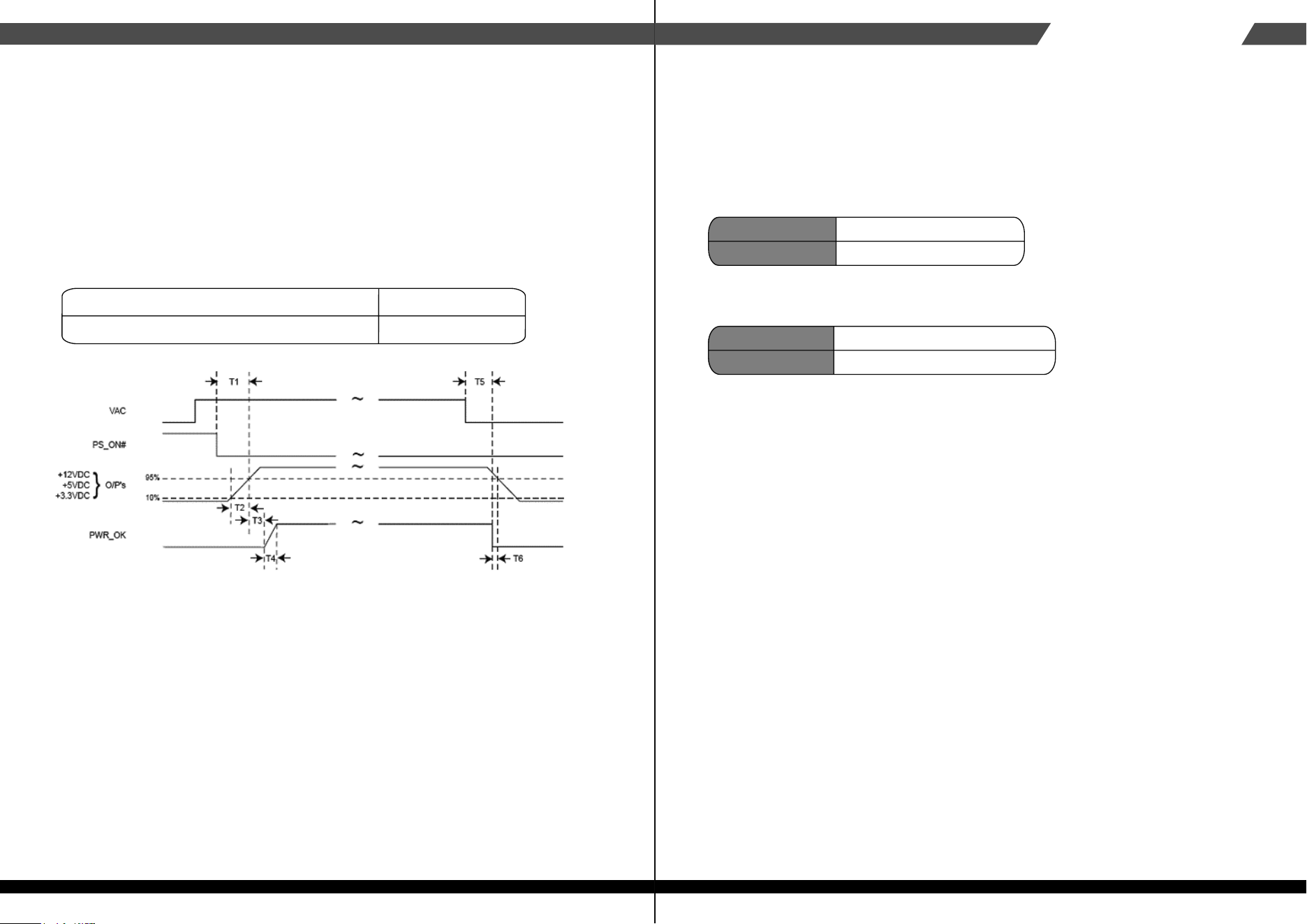
Figure:
T1: Power-on time shall be less than 500 ms (T1 < 500 ms).
T2: Rise time : 0.1 ms to 20 ms (0.1 ms ≤T2 ≤20 ms).
T3: Power-ok delay time: 100 ms < T3 < 500 ms
T4: Power-ok rise time: T4 ≤10 ms
T5 + T6: AC loss to output hold-up time :T5 + T6 ≥17 ms
POWER GOOD @ 115/230V,FULL LOAD 100 –500mSec.
POWER FAIL @115/230V,FULL LOAD 1 mSec. minimum
5. FAN NOISE REQUIREMENTS
5.1.The subject power supply is cooled by a self-contained,
80mm×15mm, 12VDC fan.
06
6. ENVIRONMENTAL REQUIREMENTS
6.1. TEMPERATURE RANGE
The power supply will be compliant with each item in this specification for the
following Environmental conditions.
The subject power supply will withstand the following imposed conditions without
experiencing non-recoverable failure or deviation from specified output characteristics.
Vibration Operating – Sine wave excited, 0.25 G maximum acceleration, 10-250 Hz
swept at one octave / min. Fifteen minute dwell at all resonant points, where resonance
is defined as those exciting frequencies at which the device under test experiences
excursions two times large than non-resonant excursions.
Plane of vibration to be along three mutually perpendicular axes.
Operating +10 to +50 deg. C
Storage -20 to +80 deg. C
6.2. HUMIDITY
6.3. VIBRATION
6.4. GROUND LEAKAGE CURRENT
The power supply ground leakage current shall be less than 3.5 mA.
6.5. DIELECTRIC STRENGTH
Primary to Frame Ground : 1800 Vac for 1 sec.
Primary to Secondary : 1800Vac for 1 sec
Operating 5 –95% RH, Non-condensing
Storage 5 –95% RH, Non-condensing
SFX Form Factor
07
7. MECHANICAL REQUIREMENTS
7.1 Physical Dimension
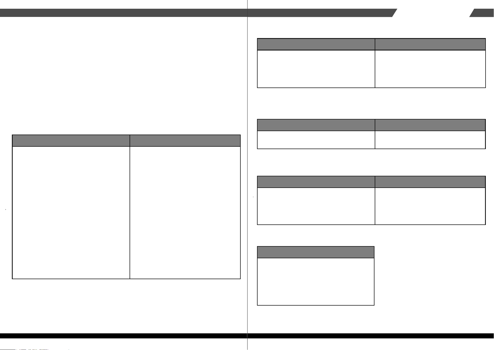
7.2 Connectors
M/B 24PIN connector
125 mm (W) × 63.5 mm (H) × 100mm (D)
Signal Pin Pin Signal
Orange +3.3V
Orange +3.3Vsense
Blue -12VDC
Black COM
Green PS-ON
Black COM
Black COM
Black COM
White N/C
Red +5VDC
Red +5VDC
Red +5Vsense
Red +5VDC
Black COM
1 +3.3V
2 +3.3V
3 COM
4 +5VDC
5 COM
6 +5VDC
7 COM
8 PWRGOOD
9 5Vsb
10 +12V
11 +12V
12 +3.3V
Orange
Orange
Black
Red
Black
Red
Black
Grey
Purple
Yellow
Yellow
Orange
13
13
14
15
16
17
18
19
20
21
22
22
23
24
6.6. INSULATION RESISTANCE
Primary to Frame Ground : 20 Meg.ohms Minimum
Primary to Secondary : 20 Meg.ohms Minimum
08
ATX 12V 4PIN (4+4PIN EPS 12V in split mode)
Signal Pin Pin Signal
Black GND
Black GND
1
2
3 +12V Yellow
4 +12V Yellow
SATA connector
Signal Pin
Orange +3.3V
Black COM
Red +5V
Black COM
Yellow +12V
5
4
3
2
1
4PIN peripheral connector (HDD) 4PIN floppy connector (FDD)
Signal Pin Pin Signal
Yellow +12V
Black COM
Black COM
Red +5VDC
1
2
3
4
1 +5VDC
2 COM
3 COM
4 +12V
Red
Black
Black
Yellow
EPS 12V 8PIN connector
Signal Pin Pin Signal
Yellow +12V
Yellow +12V
Yellow +12V
Yellow +12V
5
6
7
8
1 COM Black
2 COM Black
3 COM Black
4 COM Black
SFX Form Factor
09
8PIN PCI Express connector
Signal Pin Pin Signal
Yellow +12V
Yellow +12V
Yellow +12V
Black sense1 COM
1
2
3
4
5 COM
6 COM
7 COM
8 COM
Black
Black
Black
Black
6PIN PCI Express connector
Signal Pin Pin Signal
Yellow +12V
Yellow +12V
Yellow +12V
1
2
3
4 COM
5 COM
6 COM
Black
Black
Black
10
SFX Form Factor