TL3228X开发板使用手册
UM-TL3228X-C3 22 Ver 1.0.2
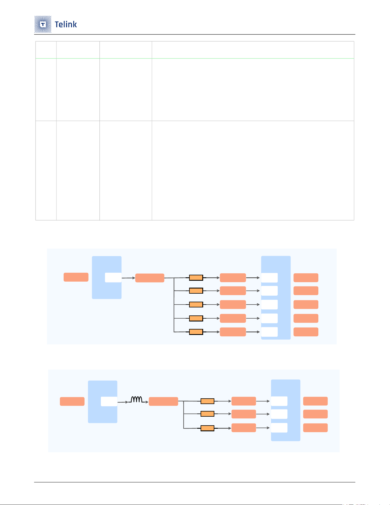
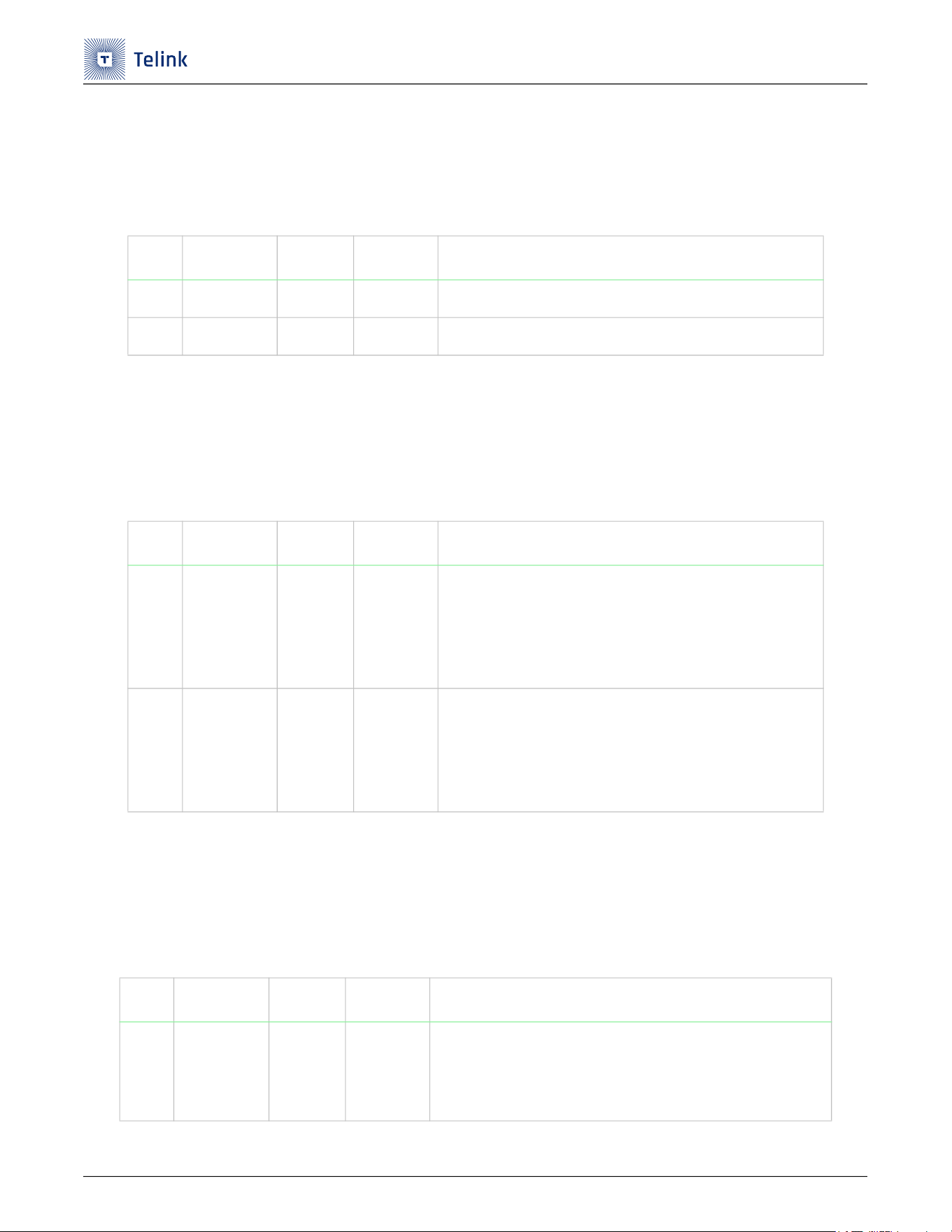
下图显示了芯片 3V3 支路连接关系。
Figure 2-3 芯片3V3支路
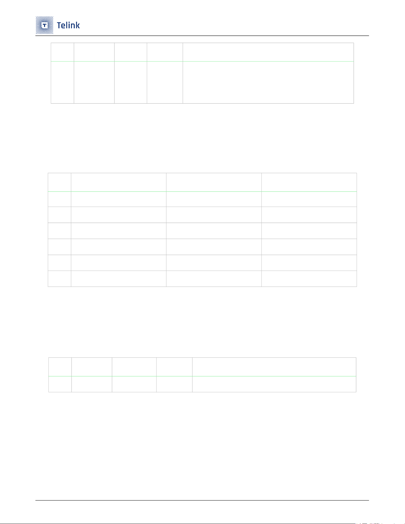
下图显示了芯片 1V2 支路连接关系。
Figure 2-4 芯片1V2支路
2
芯片3V3支
路电流
TL_VDDO3
TL_VDDIO_AMS
TL_VDD3DCDC
TL_AVDD3
(1) 芯片U2 PIN49接入1.7V~4.5V电压后,会产生1.7V~4.5V支路电压,网络名
为TL_VDDO3。
(2) 芯片U2 PIN56是3V3支路电压输出源头。
(3) 芯片U2 PIN56和U2 PIN57/PIN58/PIN44通过R42/R43/R44三个0Ω电阻
分别短接到一起,给芯片内部供电。
3
芯片1V2支路
电流
TL_VDD1P2
(1) 芯片U2 PIN49接入1.7V~4.5V电压后,会产生1V2支路电压。
(2) 芯片U2 PIN45是1V2支路电压输出源头。
(3) 芯片U2 PIN45和U2 PIN47/PIN46/PIN69通过R39/R40/R41三个0Ω电阻
分别短接到一起,然后给数字模块(PIN46)、模拟模块(PIN47)和RF模块
(PIN69)分别供电。
(4) 芯片1V2这路电源因为给RF部分供电,考虑到DCDC效率高,因此应用中
这路电源通常配置为1.2V DCDC模式。
(5) 断开R41 0Ω电阻,串入电流表,那么可以测试RF工作电流。
序号 测试项 供电 描述
U2
TL3228X
PIN56
VDDO3
TL_VBAT
TL_VDD3DCDC
TL_VDDIOAMS
U2
TL3228X
PIN49
PIN57
PIN44
PIN58
AVDD3
VDD3DCDC
VDDIOAMS
VDDIOPETL_VDDIOPE
PIN20
VBAT
TL_AVDD3
TL_VDDO3
R43(0ȍ)
R47(NC)
R44(0ȍ)
R42(0ȍ)
R45(0ȍ)
U2
TL3228X
PIN45VDD1P2
TL_VDD1P2
TL_VLINE
TL_DVDD1P2
U2
TL3228X
PIN47
PIN46
PIN69
DVDD1P2
VLINE
AVDD1P2
TL_AVDD1P2
R40(0ȍ)
R39(0ȍ)
R41(0ȍ)
TL3228X开发板使用手册
UM-TL3228X-C3 23 Ver 1.0.2
2.4 RF测试
TL3228X 开发板提供了对 RF 进行传导测试和辐射测试的方法。
下表列出了 RF 测试的方法。
Table 2-4 RF测试方式
2.5 GPIO接口
TL3228X 开发板将所有 GPIO 都接到了连接器上,方便用户使用。
下表列出了所有 GPIO 的连接去处。
Table 2-5 GPIO连接去处
序号 测试项 连接器 描述
1
RF测试
J1
(1) TL3228X开发板正常上电。
(2) RF传导测试:将J1 SMA连接器连接到测试仪器上即可进行RF传导测试。
(3) RF辐射测试:将套件中的鞭状天线连接到J1 SMA连接器上即可进行RF辐射测试。
序号 芯片脚位
IO名称
连接器
1 U2.PIN08 PH0 J7 PIN38
2
U2.PIN09 PH1 J7 PIN37
3
U2.PIN10 PH2 J7 PIN36
4
U2.PIN11 PH3 J7 PIN35
5
U2.PIN12 PH4 J7 PIN34
6
U2.PIN13 PH5 J7 PIN33
7
U2.PIN14 PH6 J7 PIN32
8
U2.PIN15 PH7 J7 PIN31
9 U2.PIN21 PE0 J7 PIN30
10 U2.PIN22 PE1 J7 PIN29
11 U2.PIN23 PE2 J7 PIN28
12 U2.PIN24 PE3 J7 PIN27
13 U2.PIN25 PE4 J7 PIN26
14 U2.PIN26 PE5 J7 PIN24
15 U2.PIN27 PE6 J7 PIN22
TL3228X开发板使用手册
UM-TL3228X-C3 24 Ver 1.0.2
16 U2.PIN28 PE7 J7 PIN21
17 U2.PIN30 PA0 J7 PIN19
18 U2.PIN31 PA1 J7 PIN20
19 U2.PIN32 PA2 J7 PIN18
20 U2.PIN35 PA5 J7 PIN16
21 U2.PIN36 PA6 J7 PIN14
22 U2.PIN40 PC5 J7 PIN10
23 U2.PIN41 PC6 J7 PIN08
24 U2.PIN42 PC7 J7 PIN06
25 U2.PIN52 PB4 J7 PIN04
26 U2.PIN53 PB5 J7 PIN03
27 U2.PIN54 PB6 J7 PIN02
28 U2.PIN55 PB7 J7 PIN01
29 U2.PIN60 PC0 J8.PIN02
30 U2.PIN61 PC1 J8.PIN06
31 U2.PIN62 PC2 J8.PIN10
32 U2.PIN63 PC3 J8.PIN12
33 U2.PIN64 PC4 J7.PIN12
34 U2.PIN70 PB0 J8.PIN14
35 U2.PIN71 PB1 J8.PIN13
36 U2.PIN72 PB2 J8.PIN16
37 U2.PIN73 PB3 J8.PIN15
38 U2.PIN74 PD0 J8.PIN18
39 U2.PIN75 PD1 J8.PIN17
40 U2.PIN76 PD2 J8.PIN20
41 U2.PIN77 PD3 J8.PIN19
42 U2.PIN78 PF0 J8.PIN22
43 U2.PIN79 PF1 J8.PIN24
序号 芯片脚位
IO名称
连接器
TL3228X开发板使用手册
UM-TL3228X-C3 25 Ver 1.0.2
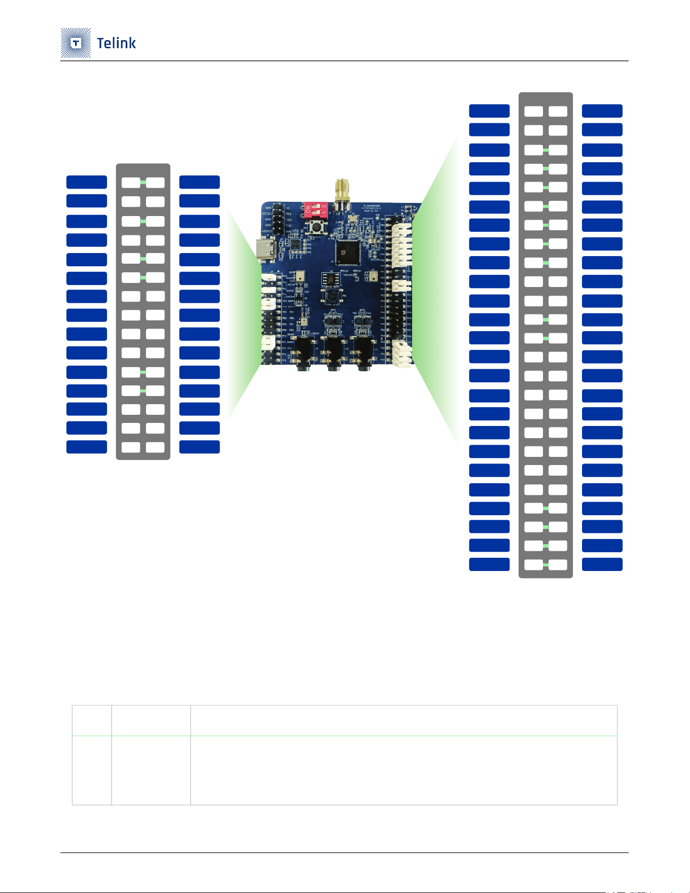
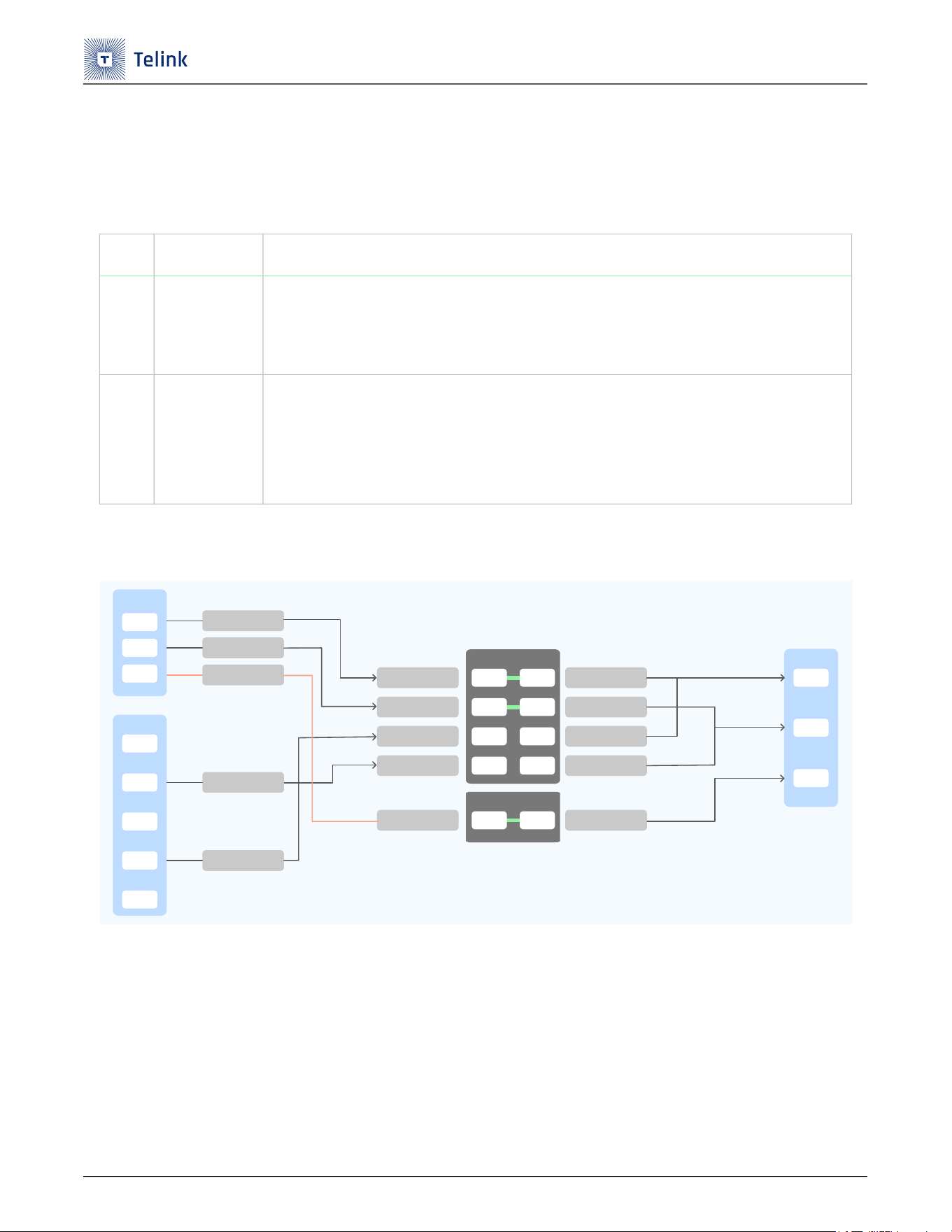
下图显示了 J7 和 J8 所有管脚的网络名,便于查询。
44 U2.PIN80 PF2 J8.PIN26
45 U2.PIN81 PF3 J8.PIN25
46 U2.PIN82 PF4 J8.PIN28
47 U2.PIN83 PF5 J8.PIN27
48 U2.PIN84 PF6 J8.PIN30
49 U2.PIN85 PF7 J8.PIN29
50 U2.PIN86 PG0 J7 PIN50
51 U2.PIN87 PG1 J7 PIN48
52 U2.PIN88 PG2 J7 PIN46
53 U2.PIN89 PG3 J7 PIN44
54 U2.PIN90 PG4 J7 PIN42
55 U2.PIN91 PG5 J7 PIN41
56 U2.PIN92 PG6 J7 PIN40
57 U2.PIN93 PG7 J7 PIN39
序号 芯片脚位
IO名称
连接器
TL3228X开发板使用手册
UM-TL3228X-C3 26 Ver 1.0.2
Figure 2-5 芯片J7和J8所有管脚
2.6 外设接口 - USB转UART
TL3228X 开发板设计了 USB 转 UART 连接器,支持 UART 通信。
下表列出了 USB 转 UART 的配置方法。
Table 2-6 USB转UART的配置
序号 配置项 描述
1
USB转UART
(1) J4 USB座子通过U1 USB转UART芯片连接到U2 TL3228X芯片的PIN16 (PD7)和PIN17
(PD6)。
(2) 使用该功能时,默认将U2的PD7设置为UART_RX,PD6设置为UART_TX。
PC1
PC1
PC3
PC2
PB2
PB0
PD2
PD0
PIN6
PIN8
PIN10
PIN12
PIN14
PIN16
PIN18
PIN20
PIN22
PIN24
PIN26
PIN28
PIN30
J8
PIN19
PIN21
PIN23
PIN25
PIN27
PIN29
PIN2
PIN4
PC0
PC0
PF1
PF0
PF4
PF2
PF6
PIN7
PIN9
PIN11
PIN13
PIN15
PIN17
PIN1
PIN3
PIN5
LINEIN_N
AMIC_N
SDMN1
SDMP1
PB3
PB1
PD3
PD1
LINEIN_P
AMIC_P
SDMP0
SDMN0
PF5
PF3
PF7
PC6
PC7
PC4
PC5
PA5
PA6
PA1
PA2
PIN6
PIN8
PIN10
PIN12
PIN14
PIN16
PIN18
PIN20
PIN22
PIN24
PIN26
PIN28
PIN30
J7
PIN19
PIN21
PIN23
PIN25
PIN27
PIN29
PIN2
PIN4
PB4
PB6
PE5
PE6
PE2
PE4
PE0
PIN7
PIN9
PIN11
PIN13
PIN15
PIN17
PIN1
PIN3
PIN5
LED_B
LED_R
LED_G
LED_W
NC
NC
PA0
MICBIAS
PB5
PB7
DMICDAT
PE7
PE3
DMICCK
PE1
PH6
PH2
PH4
PG6
PH0
PIN32
PIN34
PIN36
PIN38
PIN40
PIN42
PIN44
PIN46
PIN48
PIN50
PIN39
PIN41
PIN43
PIN45
PIN47
PIN49
PG3
PG4
PG1
PG2
PG0
PIN31
PIN33
PIN35
PIN37
PH7
PH3
PH5
PG7
PH1
KEY1
PG5
KEY3
KEY2
KEY4
TL3228X开发板使用手册
UM-TL3228X-C3 27 Ver 1.0.2
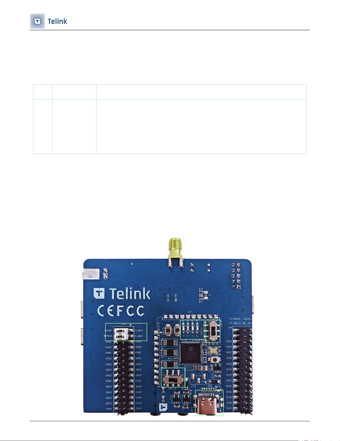
2.7 外设接口 - BEVK模块
TL3228X 开发板设计了板载 BEVK 模块,便于 debug 调试。
下表列出了板载 BEVK 模块 debug 调试的配置方法。
Table 2-7 BEVK模块debug调试的配置
BEVK模块使用说明
Step 1 J12 USB Type-C 连接电脑,红灯亮表示正常供电。
Step 2 绿灯闪烁表示 BEVK 模块正常工作。
Step 3 SW15 开关拨向右边。
Step 4 SW13 开关拨向下边。
Step 5 确认跳帽是否正常跳接。
Figure 2-6 BEVK模块
序号 配置项 描述
1
板载BEVK模块
debug调试
(1) 当前版本使用的BEVK模块,可以配合5.9.0及以上版本BDT使用。
(2) 接USB后,J13 BL3V3、EXT3V3与TLVBAT使用跳帽连接,BEVK模块上的SW15右拨
(左拨时BEVK的SWS或JTAG断开与U2连接),SW13下拨(上拨为JTAG模式),即可
正常调试。
(3) BEVK模块绿灯为SWS模式,蓝灯为JTAG模式。
5
24
3
1
TL3228X开发板使用手册
UM-TL3228X-C3 28 Ver 1.0.2
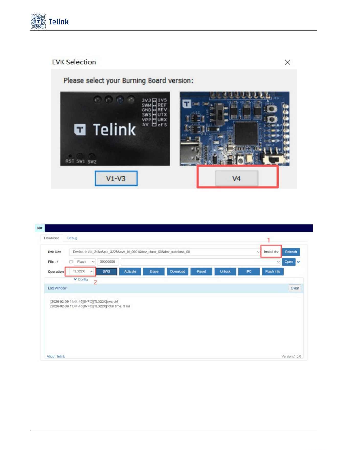
Step 6 使用泰凌 BDT 工具,需要 5.9.0 以上版本,选择 V4。
Figure 2-7 EVK选择
Step 7 第一次使用时需要点击 ”Install drv” 安装驱动。
Step 8 选择对应的芯片即可使用。
Figure 2-8 安装驱动和选择芯片
TL3228X开发板使用手册
UM-TL3228X-C3 29 Ver 1.0.2
2.8 外设接口 - USB Type-C (HS)
TL3228X 开发板设计了 USB Type-C 连接器,便于供电和支持 USB 通信。
下表列出了所有 DM 和 DP 的连接去处。
Table 2-8 USB的DM和DP
2.9 外设接口 - 32.768KHz晶振
TL3228X 开发板内置 32KHz RC 电路,同时也支持外置 32.768KHz 晶振。
下表列出了 32.768KHz 晶振管脚的连接方式。
Table 2-9 32.768KHz晶振的连接方式
2.10 外设接口 - DMIC
TL3228X 开发板设计了两个 DMIC,型号是 WMM7047DTFN0,便于做演示。
下表列出了 DMIC 管脚的连接方式。
Table 2-10 DMIC的管脚连接方式
序号 芯片脚位
IO名称
连接器 描述
1 U2.PIN33 PA4 J6
连接到USB的DM管脚。
2 U2.PIN34 PA3 J6
连接到USB的DP管脚。
序号 芯片脚位
IO名称
连接器 描述
1 U2.PIN62 PC2 J8.PIN10
(1) 支持配置为GPIO和外置32.768K crystal功能。默认功能
作GPIO,通过R6 0Ω来连接到外部外置32.768K crystal,
以便于测试GPIO和使能外置32.768K crystal功能。
(2) 管脚位置参考Figure 2-5
2 U2.PIN63 PC3 J8.PIN12
(1) 支持配置为GPIO和外置32.768K crystal功能。默认功能
作GPIO,通过R7 0Ω来连接到外部外置32.768K crystal,
以便于测试GPIO和使能外置32.768K crystal功能。
(2) 管脚位置参考Figure 2-5
序号 芯片脚位
IO名称
连接器 描述
1 U2.PIN25 PE4 J7.PIN26
(1) 连接到J7 PIN26,然后通过跳帽连接到J7 PIN25。
(2) 连接到DMIC的数据管脚。
(3) 管脚位置参考Figure 2-5
TL3228X开发板使用手册
UM-TL3228X-C3 30 Ver 1.0.2
2.11 外设接口 - Flash
TL3228X 开发板上装配了外置 flash,型号为 P25Q16SU,便于客户扩展使用或者验证新的 flash.
下表列出了 flash 管脚的连接方式。
Table 2-11 Flash管脚连接方式
2.12 外设接口 - IR
TL3228X 开发板上设计了红外调试电路,便于做演示。
下表列出了 IR 管脚的连接方式。
Table 2-12 IR的管脚连接方式
2 U2.PIN26 PE5 J7.PIN24
(1) 连接到J7 PIN24,然后通过跳帽连接到J7 PIN23。
(2) 连接到DMIC1的时钟管脚。
(3) 管脚位置参考Figure 2-5
序号 芯片脚位
IO名称
Flash
1 U2.PIN01 PI0 U5.PIN05
2
U2.PIN02 PI1 U5.PIN06
3
U2.PIN03 PI2 U5.PIN07
4
U2.PIN04 PI3 U5.PIN01
5
U2.PIN05 PI4 U5.PIN02
6
U2.PIN06 PI5 U5.PIN03
序号 芯片脚位
IO名称
连接器 描述
1 U2.PIN51 IR -
直接连接到IR部分的电路。
序号 芯片脚位
IO名称
连接器 描述
TL3228X开发板使用手册
UM-TL3228X-C3 31 Ver 1.0.2
2.13 上行通路接口
TL3228X 开发板上行链路支持一路 AMIC,一路差分 LINE-IN 通路配置。以上都可以通过跳线进行配置。
下表列出了上行通路的配置方法。
Table 2-13 上行通路的配置
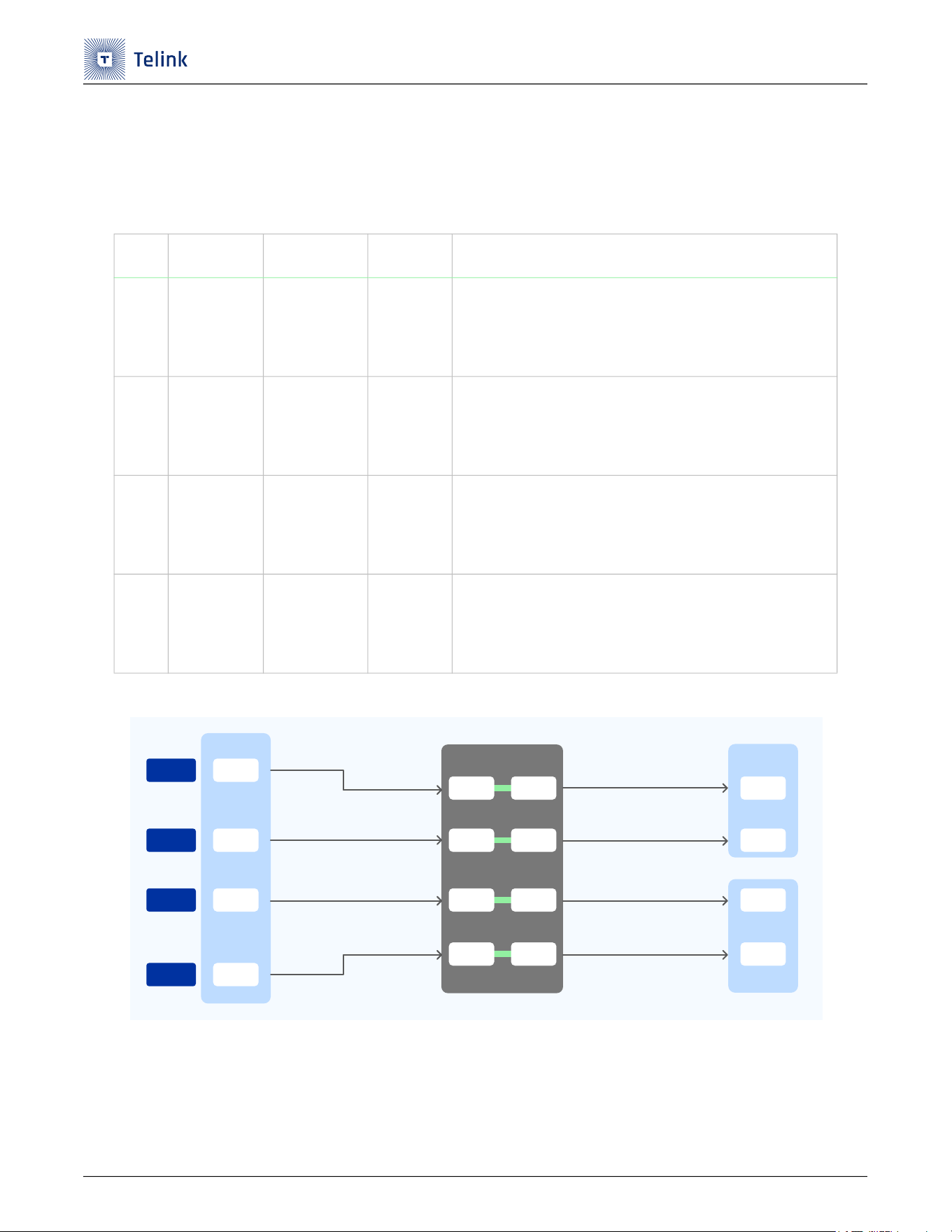
下图显示了差分 AMIC 和 LINE-IN 上行通路的连接关系。
Figure 2-9 差分AMIC和LINE-IN上行通路的关系
序号 配置项 描述
1
一路差分
AMIC配置
(1) 开发板的默认接法是一路差分AMIC配置。
(2) J8的PIN2-PIN1和J8的PIN6-PIN5共2个跳帽默认连接。
(3) 管脚位置参考Figure 2-9
2
一路差分
LINE-IN配置
(1) 拔掉J8的PIN2-PIN1和J8的PIN6-PIN5的2个跳帽。
(2) 插上J8的PIN4-PIN3和J8的PIN8-PIN7的2个跳帽。
(3) 此时可以通过J9的3.5mm插座连接到音频测试仪器上采用差分解法进行uplink性能测试。
(4) 管脚位置参考Figure 2-9
U7
PIN01
AIPL1_MIC
PIN02
PIN04
J9
PIN01
PIN02
PIN04
PIN03
PIN05
AINL1_MIC
MICBIAS_AIL1
AINL1_LINEIN
AIPL1_LINEIN
J8
PIN02 PIN01
PIN06 PIN05
PIN04 PIN03
PIN08 PIN07
AIPL1_MIC
AINL1_MIC
AIPL1_LINEIN
AINL1_LINEIN
MICBIAS_AIL1
TL_AIPL1
TL_AINL1
TL_AIPL1
TL_AINL1
TL_MICBIAS
U2
PIN60
PIN61
PIN32
J7
PIN18 PIN17
TL3228X开发板使用手册
UM-TL3228X-C3 32 Ver 1.0.2
2.14 下行通路接口
TL3228X 开发板下行链路支持两路 SDM 差分输出。注意,不支持单端配置。
下表列出了下行通路的配置方法。
Table 2-14 下行通路的配置
Figure 2-10 下行通路的连接关系
序号 芯片脚位
IO名称
连接器 描述
1 U2.PIN78 PF0 J8.PIN22
(1) 连接到J8 PIN22,然后通过跳帽连接到J8 PIN21。
(2) 通过SDM的相关电路之后,连接到J11 PIN02。
(3) 管脚位置参考Figure 2-10
2 U2.PIN79 PF1 J8.PIN24
(1) 连接到J8 PIN24,然后通过跳帽连接到J8 PIN23。
(2) 通过SDM的相关电路之后,连接到J11 PIN03。
(3) 管脚位置参考Figure 2-10
3
U2.PIN62 PC2 J8.PIN10
(1) 连接到J8 PIN10,然后通过跳帽连接到J8 PIN09。
(2) 通过SDM的相关电路之后,连接到J10 PIN02。
(3) 管脚位置参考Figure 2-10
4
U2.PIN63 PC3 J8.PIN12
(1) 连接到J8 PIN12,然后通过跳帽连接到J8 PIN11。
(2) 通过SDM的相关电路之后,连接到J10 PIN03。
(3) 管脚位置参考Figure 2-10
U2
PIN78
PIN79
PIN62
PIN63
J8
PIN22 PIN21
PIN24 PIN23
PIN10 PIN09
PIN12 PIN11
J11
PIN02
PIN03
PIN02
PIN03
J10
PF0
PF1
PC2
PC3
TL3228X开发板使用手册
UM-TL3228X-C3 33 Ver 1.0.2
3 相关文档
下表列出了一些其他文档和资源,您可以参考这些文档和资源以获取更多信息。其中一些文档仅在签订保密协议
(NDA)的情况下提供。要访问此类文档,请联系当地的泰凌现场应用工程师 (FAE)或销售代表。
Table 3-1 相关文档
序号 文档名称 描述
链接/获取方式
1 TL322x/TL382x datasheet
提供了关于TL322x/TL382x的电气
特性,硬件说明和订购方式等信息。
TL322x/TL382x datasheet
2
TL322x/TL382x hardware
guideline
提供了TL322x/TL382x硬件设计注
意事项。
TL322x_Hardware_Design_Guideline
3 TL3228X board files
提供了TL3228X开发板的原理图、
PCB等设计文件。
TL3228X board files
TL3228X开发板使用手册
UM-TL3228X-C3 34 Ver 1.0.2
4 认证声明
4.1 FCC Statement
This device complies with Part 15 of the FCC rules. Operation is subject to the following two conditions: (1)
this device may not cause harmful interference, and (2) this device must accept any interference received,
including interference that may cause undesired operation.
This equipment has been tested and found to comply with the limits for a Class B digital device, pursuant to
Part 15 of the FCC rules. These li
mits are designed to provide reasonable protection against harmful
interference in a residential installation. This equipment generates, uses and can radiate radio frequency
energy and if not installed and used in accordance with the instructions, may cause harmful interference to
radio communications. However, there is no guarantee that interference will not occur i
n a particular
installation. If this equipment does cause harmful interference to radio or television reception, which can be
determined by turning the equipment off and on, the user is encouraged to try to correct the interference by
one or more of the following measures:
• Reorient the receiving antenna.
• Increase the separation between the equipment and receiver.
• Connect the equipment into and outlet on a ci
rcuit different from that to which the receiver is
connected.
• Consult the dealer or an experienced radio/TV technician for help.
Changes or modifications not expressly approved by the party responsible for compliance could void your
authority to operate the equipment. The distance between user and products should be no less than 20cm.
The EUT is In door use only.
