UMxxxx - Draft – June 2025
.
www.st.com
UMxxxx
User manual
STM32WBA Nucleo-64 board (MB1801 and MB2293)
Introduction
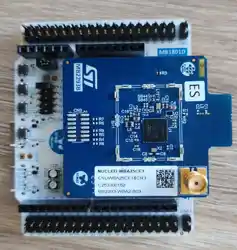
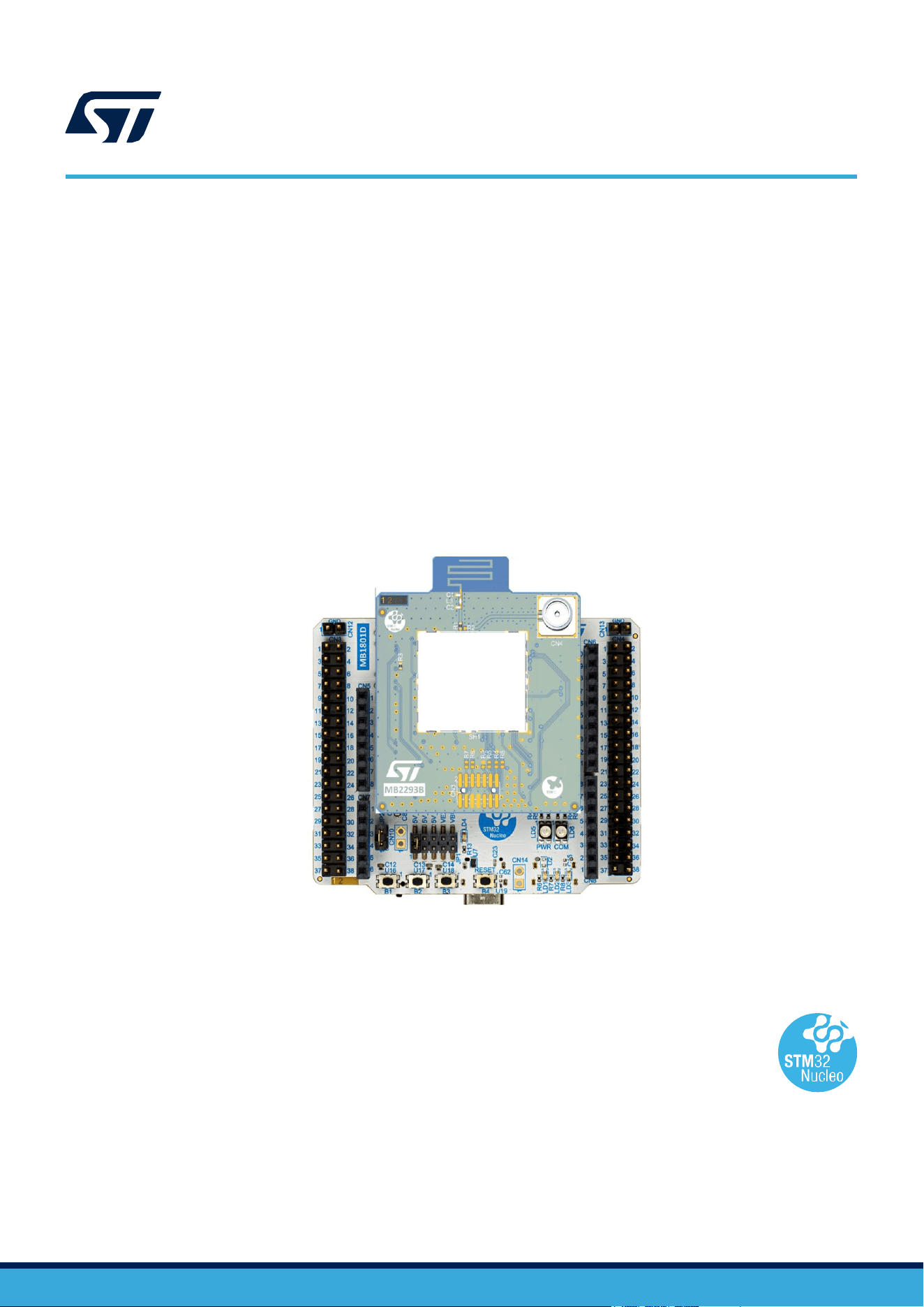
The NUCLEO-WBA25CE1 STM32 Nucleo-64 board, based on the MB1801 mezzanine board and the MB2293 MCU RF board,
is a wireless and ultra‑low‑power board embedding a powerful and ultra‑low‑power radio compliant with the Bluetooth
®
LE,
IEEE 802.15.4-2015 PHY and MAC, supporting Thread, Matter, and Zigbee
®
.
A user USB Type-C
®
is also provided for easy connection with other devices.
The ARDUINO
®
Uno V3 connectivity support and the ST morpho headers allow the easy expansion of the functionality of the
STM32 Nucleo open development platform with a wide choice of specialized shields.
Figure 1. NUCLEO-WBA25CE1 global view
Picture is not contractual.
UMxxxx - Draft
page 2/48
UMxxxx
Features
1
Features
• Ultra‑low‑power wireless STM32WBA25CEU7 microcontroller based on the Arm
®
Cortex
®
‑M33
core, featuring 512 Kbytes of flash memory and 96 Kbytes of SRAM in a UFQFPN48 package
• MCU RF board (MB2293):
– 2.4 GHz RF transceiver supporting Bluetooth
®
LE specification v6.0
– Build-in PCB antenna
• Three user LEDs
• Three user push-buttons and one reset push-button
• Board connectors:
◦ User USB Type-C
®
◦ USB Type-C
®
for debugging purpose
◦ ARDUINO
®
Uno V3 expansion connector
◦ ST morpho headers for full access to all STM32 I/Os
• Flexible power-supply options: ST-LINK USB V
BUS
or external sources
• On-board STLINK-V3EC debugger/programmer with USB re-enumeration capability: mass storage, Virtual
COM port, and debug port
• Comprehensive free software libraries and examples available with the STM32CubeWBA MCU Package
• Support of a wide choice of Integrated Development Environments (IDEs) including IAR Embedded
Workbench
®
, MDK-ARM, and STM32CubeIDE
Note: Arm and TrustZone are registered trademarks of Arm Limited (or its subsidiaries) in the US and/or elsewhere.
UMxxxx - Draft
page 3/48
UMxxxx
Ordering information
2
Ordering information
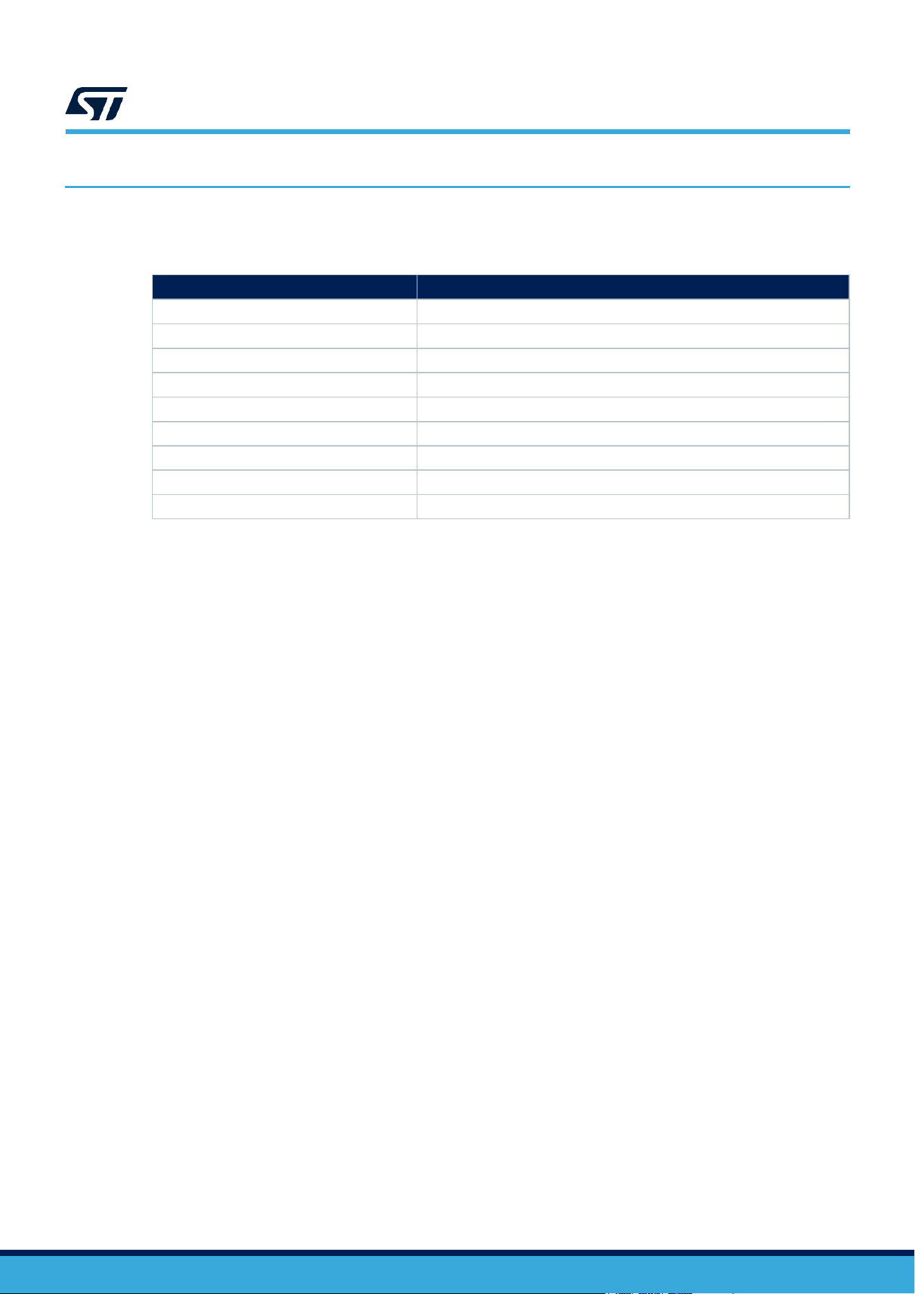
To order the NUCLEO-WBA25CE1 board, refer to Table 1. Additional information is available from the
datasheet and reference manual of the target microcontroller.
Table 1. List of available products
Order code
Board reference
Target STM32
NUCLEO-WBA25CE1
• MB1801
(1)
• MB2293
(2)
STM32WBA25CEU7
1. Mezzanine board
2. MCU RF board
2.1
Codification
The meaning of the codification is explained in Table 2.
Table 2. Codification explanation
NUCLEO-XXXYYZTU
Description
Example: NUCLEO-WBA25CE1
XXX
MCU series in STM32 32-bit Arm Cortex MCUs
STM32WBA series
YY
MCU product line in the series
STM32WBA25 product line
Z
STM32 package pin count:
• C for 48 pins
48 pins
T
STM32 flash memory size:
• E for 512 Kbytes
512 Kbytes
U
1 for Cut1.0
First version of NUCLEO-WBA25
UMxxxx - Draft
page 4/48
UMxxxx
Development environment
3
Development environment
3.1
System requirements
• Multi‑OS support: Windows
®
10, Linux
®
64-bit, or macOS
®
• USB Type-A or USB Type-C
®
to USB Type-C
®
cable
Note:
macOS
®
is a trademark of Apple Inc., registered in the U.S. and other countries and regions.
Linux
®
is a registered trademark of Linus Torvalds.
Windows is a trademark of the Microsoft group of companies.
3.2
Development toolchains
• IAR Systems
®
- IAR Embedded Workbench
®(1)
• Keil
®
- MDK-ARM
(1)
• STMicroelectronics - STM32CubeIDE
1.
On Windows
®
only.
3.3
Demonstration software
The demonstration software, included in the STM32Cube MCU Package corresponding to the on-board
microcontroller, is preloaded in the STM32 flash memory for easy demonstration of the device peripherals in
standalone mode. The latest versions of the demonstration source code and associated documentation can be
downloaded from www.st.com.
3.4
CAD resources
All board design resources, including schematics, CAD databases, manufacturing files, and the bill of materials,
are available from the NUCLEO-WBA25CE1 product page at www.st.com.
UMxxxx - Draft
page 5/48
UMxxxx
Conventions
4
Conventions
Table 3 provides the conventions used for the ON and OFF settings in the present document.
Table 3. ON/OFF convention
Convention
Definition
Jumper JPx ON
Jumper fitted
Jumper JPx OFF
Jumper not fitted
Jumper JPx [1-2]
Jumper fitted between pin 1 and pin 2
Solder bridge SBx ON
SBx connections closed by 0 Ω resistor
Solder bridge SBx OFF
SBx connections left open
Resistor Rx ON
Resistor soldered
Resistor Rx OFF
Resistor not soldered
Capacitor Cx ON
Capacitor soldered
Capacitor Cx OFF
Capacitor not soldered

UMxxxx - Draft
page 6/48
UMxxxx
Safety recommendations
5
Safety recommendations
5.1
Targeted audience
This product targets users with at least basic electronics or embedded software development knowledge such as
engineers, technicians, or students. This board is not a toy and is not suited for use by children.
5.2
Handling the board
This product contains a bare printed circuit board and like all products of this type, the user must be careful about
the following points:
• The connection pins on the board might be sharp. Be careful when handling the board to avoid hurting
yourself
• This board contains static‑sensitive devices. To avoid damaging it, handle the board in an ESD‑proof
environment.
• While powered, do not touch the electric connections on the board with your fingers or anything conductive.
The board operates at a voltage level that is not dangerous, but components might be damaged when
shorted.
• Do not put any liquid on the board and avoid operating the board close to water or at a high humidity level.
• Do not operate the board if dirty or dusty.

UMxxxx - Draft
page 7/48
UMxxxx
Quick start
6
Quick start
This section describes how to start development quickly using NUCLEO-WBA25CE1.
To use the product, you must accept the evaluation product license agreement from the www.st.com/epla
webpage.
Before the first use, make sure that no damage occurred to the board during shipment:
• All socketed components must be firmly secured in their sockets.
• Nothing must be loose in the board blister.
The Nucleo board is an easy-to-use development kit to evaluate quickly and start development with an STM32
microcontroller in a UFQFPN48 package.
6.1
Getting started
Follow the sequence below to configure the NUCLEO-WBA25CE1 board and launch the demonstration application
(refer to Figure 3 and Figure 4 for component location):
1. Check jumper positions on board: JP2 ON, JP1 on 5V_STLK.
2. Check that the power switch (SW1) is in the default position.
3. Install the ST Bluetooth
®
LE sensor mobile application on a Bluetooth
®
LE compatible mobile device from the
App Store or Google Play.
4. Connect the Nucleo board to a PC with a USB Type-A or USB Type-C
®
to USB Type-C
®
cable through the
USB_STLK USB connector (CN15).
5. Use the ST Bluetooth
®
LE sensor mobile application to detect the STM32WBA P2P server (P2PSRV) and
connect it. The smartphone application displays the service and characteristics of the device.
6. Pushing the button (B1) on the board toggles the alarm on the smartphone display. On the smartphone, push
the lamp to switch ON/OFF the Nucleo board blue LED (LD1).
UMxxxx
Hardware layout and configuration
UMxxxx - Draft
page 8/48
Three LEDs
Three push-buttons
ARDUINO
®
expansion connectors
ST morpho
expansion connectors
External components
for SMPS
7
Hardware layout and configuration
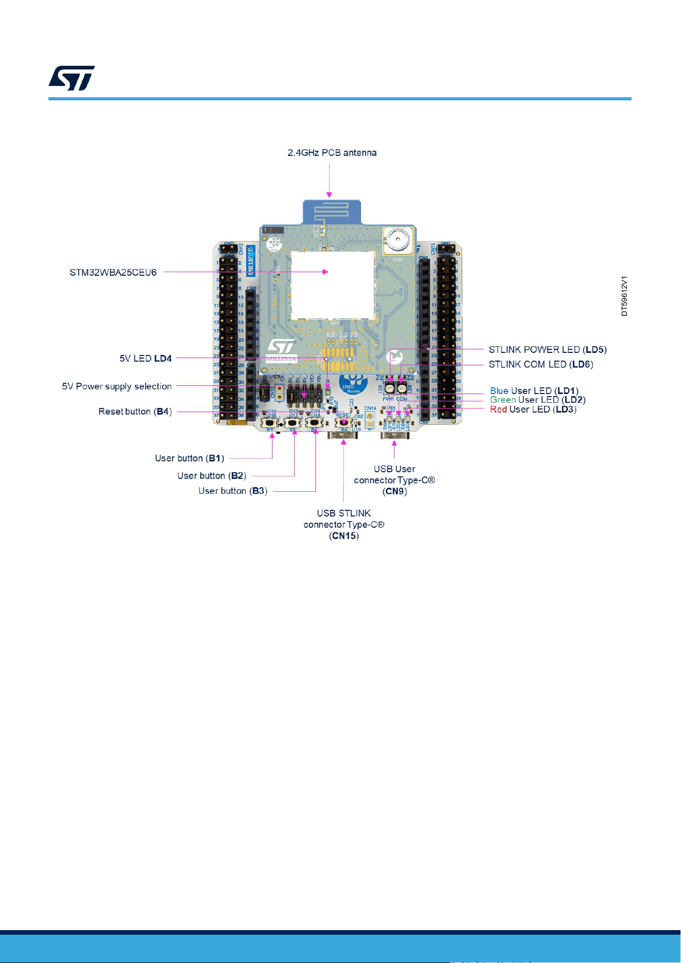
NUCLEO-WBA25CE1 is designed around the STM32WBA25CE. The design includes a mezzanine board and an
MCU RF board. The hardware block diagram in Figure 2 illustrates the connection between STM32WBA25CE
and peripherals (ARDUINO
®
Uno V3 connectors, ST morpho connector, and embedded ST-LINK).
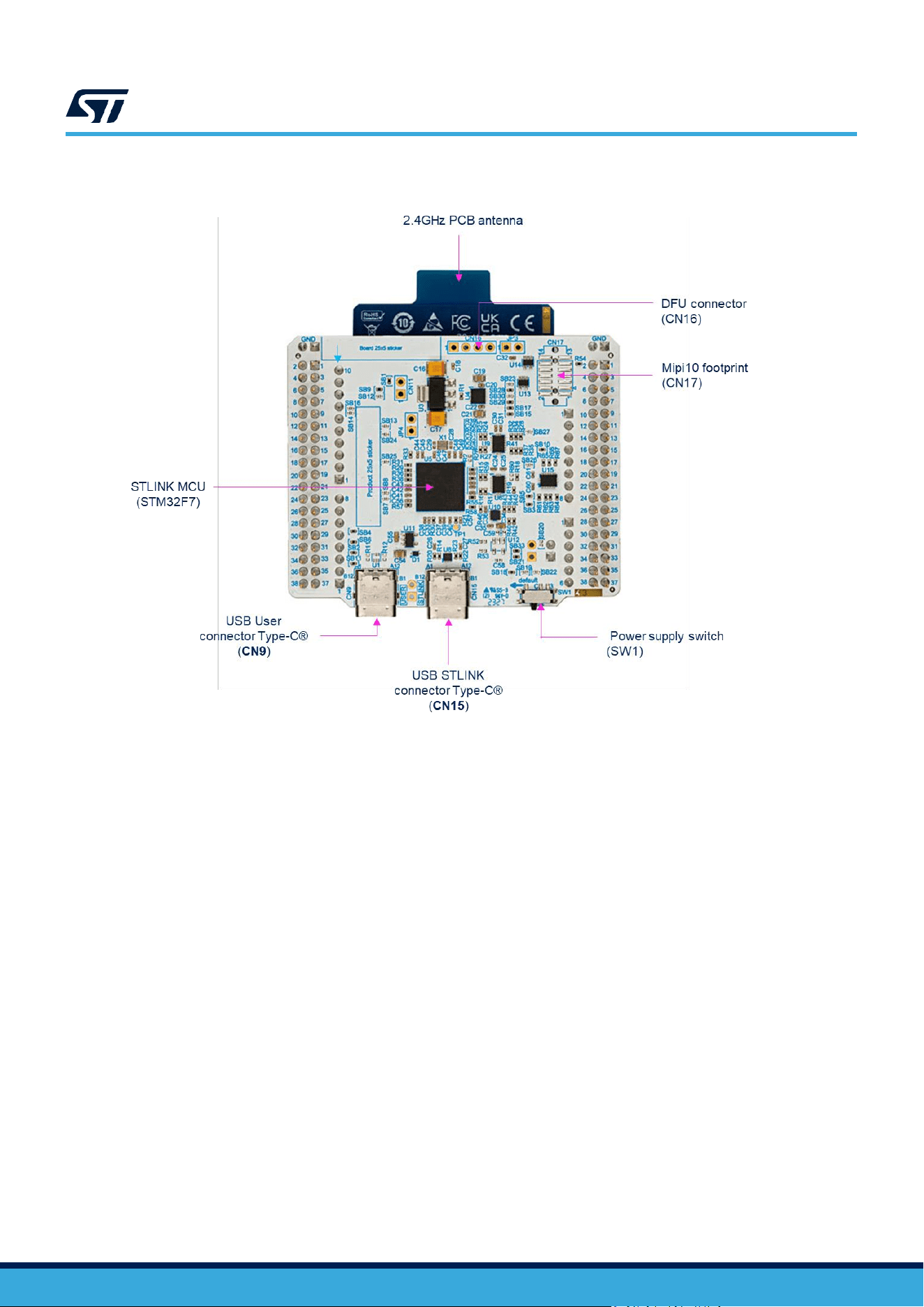
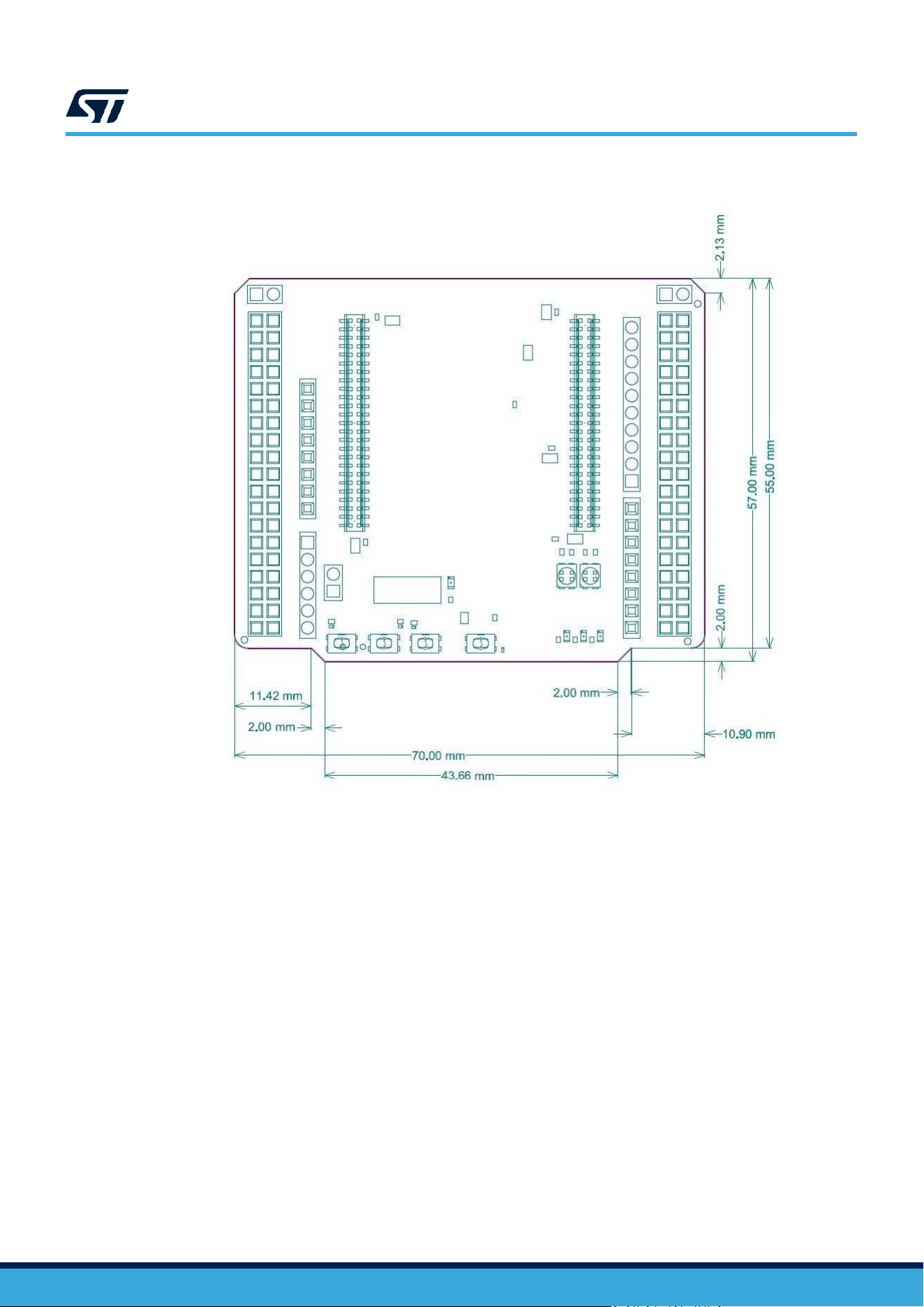
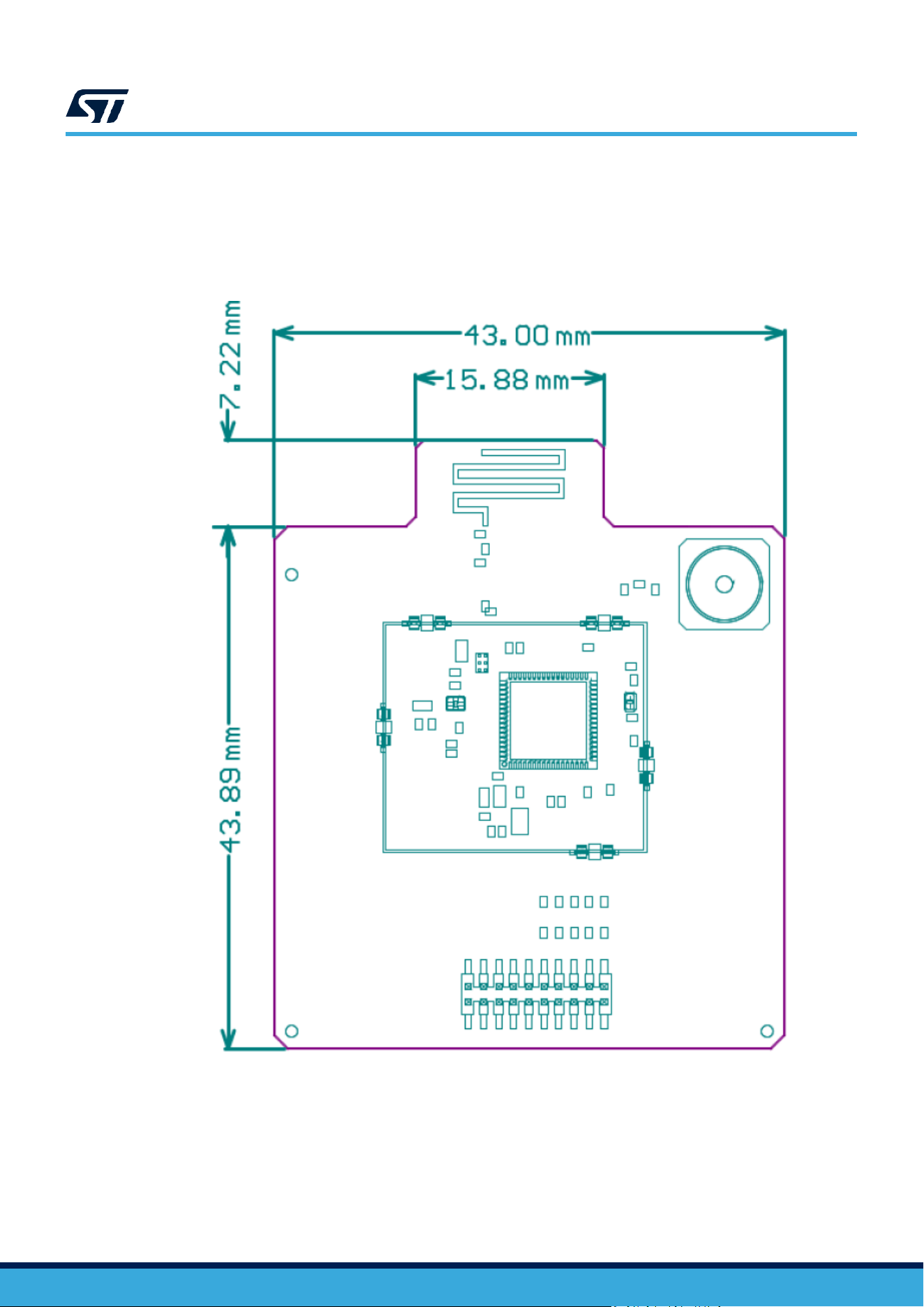
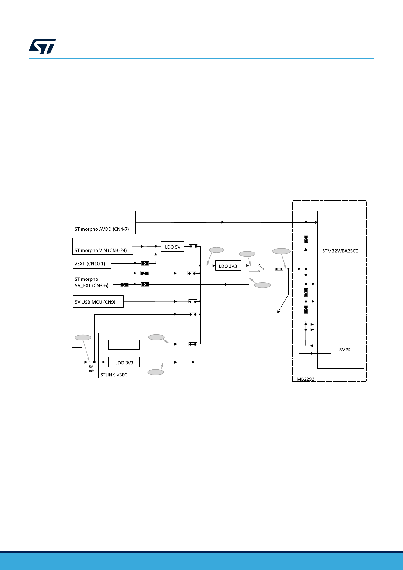
Figure 3 and Figure 4 help users locate these features on the NUCLEO-WBA25CE1 board. The mechanical
dimensions of the NUCLEO-WBA25CE1 product are shown in Figure 5 and Figure 6.
Figure 2. Hardware block diagram
NUCLEO-WBA25CE1 (MB1801+MB2293)
MB1801
Level shifter Level shifter
MB2293
STM32WBA25
Filter
matching
PCB
antenna
Board power
STM32WBA25 side
ST-LINK side
5V ST-LINK
STLINK-V3EC
STM32WBA65
Debug
RF path
GPIOs
Power management
External
power
supply
(1.8 to 3.3 V
optional)
External
power
supply
(7 to 12 V
optional)
External
power
supply
(5 V
optional)
User USB
ST-LINK USB
32 MHz
crystal
Reset
push-button
SMA
Power selector
LDO
5 to 3 V
LDO
12 to 5 V
LDO
5 to 3 V
Power selector
Level shifter
32.768 kHz
crystal
DT59611V1
UMxxxx
Hardware layout and configuration
UMxxxx - Draft
page 9/48
Figure 3. NUCLEO-WBA25CE1 PCB top view
DT59612V1
UMxxxx
Hardware layout and configuration
UMxxxx - Draft
page 10/48
Figure 4. NUCLEO-WBA25CE1 PCB bottom view
DT59613V1
UMxxxx
Hardware layout and configuration
UMxxxx - Draft
page 11/48
Figure 5. NUCLEO-WBA25CE1 (MB1801) mechanical dimensions (in millimeters)
UMxxxx
Hardware layout and configuration
UMxxxx - Draft
page 12/48
Figure 6. NUCLEO-WBA25CE1 (MB2293) mechanical dimensions (in millimeters)
UMxxxx
Hardware layout and configuration
UMxxxx - Draft
page 13/48
7.1
Power supply
7.1.1
General description
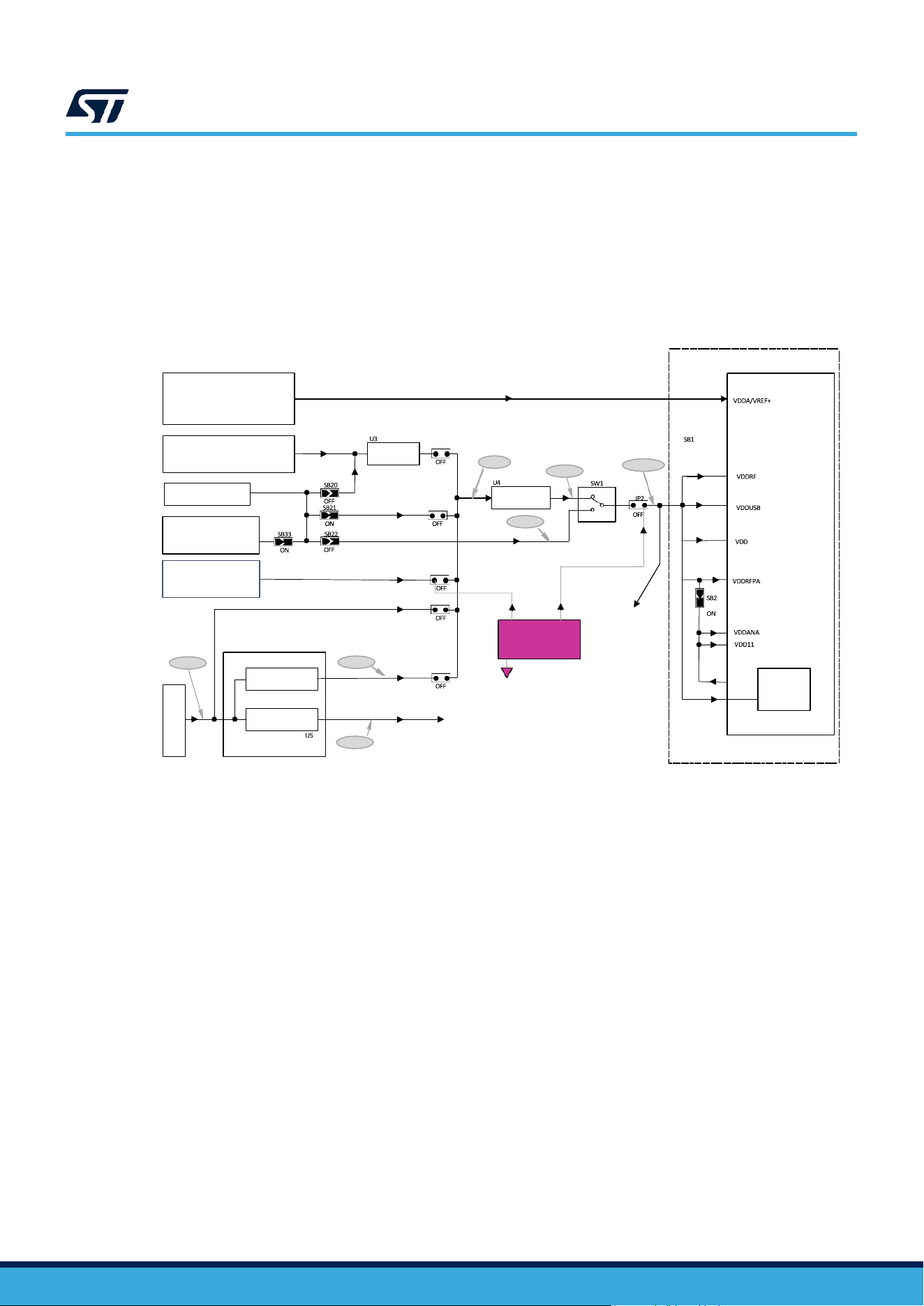
By default, the STM32WBA25CE embedded on this Nucleo board is supplied by 3V3 but the board proposes
many possibilities to supply the module. In fact, at first, the 3V3 can come from ST-LINK USB, ARDUINO
®
, or ST
morpho connectors. Moreover, STM32WBA25CE can be supplied by an external source (between 1.8 and 3.3
V). Thanks to level shifters, debugging by embedded ST-LINK is always possible even if the supply voltage of the
target is different than 3V3 (ST-LINK supply). Figure 7 shows the power tree. Moreover, this figure also shows the
default state of the jumpers and the solder bridges.
Note: The product must be supplied by a voltage source or auxiliary equipment that complies with EN
62368-1:2014+A11:2017 or the standard that replaces it. It must also be a safety extralow voltage (SELV) with
limited power capability.
Figure 7. STM32WBA25CE1 power tree
VDDA/VREF+
SB1
U3
JP1 [5-6]
ON
OFF
5V
VDD
3V3
SB20
U4
SW1
OFF
JP2
SB21
JP1 [7-8]
ON
ON
OFF
SB33
SB22
1V8 to 3V3
VDD
ON
OFF
SB6
OFF
JP1 [3-4]
VDDRFPA
OFF
JP1 [9-10]
SB41
ON
Level shifter (WBA side)
OFF
VDDANA
VDD11
VBUS_STLK
U10
Power switch
5V_STLK
JP1 [1-2]
ON
Level shifter (ST-LINK side)
U11
3V3_STLK
ARDUINO® VIN (CN5-8)
AVDDEXT (CN11-1)
ARDUINO® AVDD (CN6-8)
USB ST-LINK
DT59616V1

UMxxxx
Hardware layout and configuration
UMxxxx - Draft
page 14/48
7.1.2
7 to 12 V power supply
A 7 to 12 V DC power source can power NUCLEO-WBA25CE1. There are three accesses for this type of level:
• Pin VIN of the ARDUINO
®
connector (CN5-8). It is possible to apply until +12 V on this pin or use an
ARDUINO
®
shield, which can deliver this type of voltage on the VIN pin.
• Pin VIN of the ST morpho connector (CN3-24). It is possible to apply until +12 V on this pin like for the
ARDUINO
®
connection.
• External input (CN10). Be careful, in this case, the states of the jumpers and solder bridge are critical.
Verify these states in Table 4.
These sources are connected to a linear low‑drop voltage regulator (U2). The output of this regulator (5 V) is a
potential source of the 5V signal (refer to details in the next section).
7.1.3
5 V power supply
A 5 V DC power source can power NUCLEO-WBA25CE1. The 5 V can come from several connectors:
• External input (VEXT, CN10). Be careful, in this case, the states of the jumpers and solder bridge are
critical. Refer to Table 4.
• 5V_EXT from ST morpho connector (CN3-6 of MB1801)
• VIN (7-12 V) input through the voltage regulator (U2). Refer to Section 7.1.2: 7 to 12 V power supply.
• USB ST-LINK can supply the board directly (VBUS_STLK) or through the monitoring of STLINK-V3EC.
• 5V_USB coming from the user USB connector (CN9).
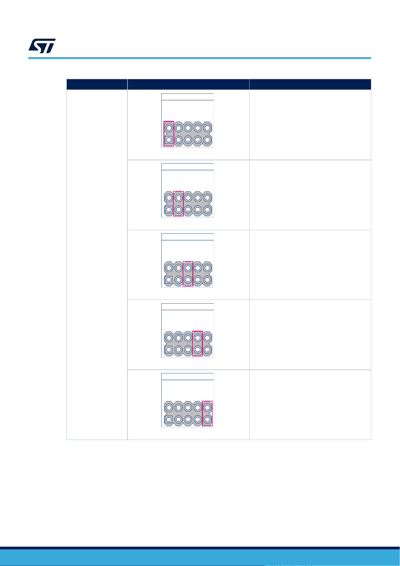
The jumper (JP1) selects the 5V source. Table 4 shows the configuration to apply the selected source.
Depending on the current needed on the devices connected to the USB port, and the board itself, power
limitations can prevent the system from working as expected. The user must ensure that NUCLEO-WBA25CE1 is
supplied with the correct power source depending on the current need.
UMxxxx
Hardware layout and configuration
UMxxxx - Draft
page 15/48
Table 4. Power supply selector (JP1) description
When 5V_STLK is used, JP1 is set to [1-2]. The sequence is specific. In the beginning, only STLINK-V3EC is
supplied. If the USB enumeration succeeds, the 5V_STLK power is enabled by asserting the PWR_EN signal
from STLINK-V3EC. This pin is connected to a power switch (U10), which supplies the rest of the board. This
power switch also features a current limitation to protect the PC in case of currents exceeding 300 mA.
NUCLEO-WBA25CE1 is supplied through the
ST- LINK USB Type-C
®
connector (CN15)
without any control from STLINK-V3EC.
JP1
10
1 9
2
5V sources
NUCLEO-WBA25CE1 is supplied through CN10
or through pin 6 of the ST morpho connector
(CN3). Refer to the configuration details in the
present Power supply section.
JP1
10
1 9
2
5V sources
NUCLEO-WBA25CE1 is supplied through pin 8
of the ARDUINO
®
connector (CN5) or pin 24 of
the ST morpho connector (CN3) or CN10 (refer
to the configuration details in the present Power
supply section).
JP1
10
1 9
2
5V sources
NUCLEO-WBA25CE1 is supplied through the
user USB Type-C
®
connector (CN9).
JP1
10
1 9
2
5V sources
Default setting
NUCLEO-WBA25CE1 is supplied through the
USB ST-LINK USB Type-C
®
connector (CN15).
ST-LINK controls this source. It enables this 5V
after the startup of STLINK-V3EC if all the
conditions are fulfilled.
JP1
10
1 9
2
5V sources
JP1
5V supply source
selector
Configuration
Setting
Jumper
5V_STLK
5V_STLK
5V_STLK
5V_STLK
5V_STLK
5V_USB
5V_USB
5V_USB
5V_USB
5V_USB
5V_INT
5V_INT
5V_INT
5V_INT
5V_INT
VEXT
VEXT
VEXT
VEXT
VEXT
VBUS_STLK
VBUS_STLK
VBUS_STLK
VBUS_STLK
VBUS_STLK
UMxxxx
Hardware layout and configuration
UMxxxx - Draft
page 16/48
7.1.4
Current measurement
As the device has low‑power features, it can be interesting to measure the current consumed by NUCLEO-
WBA25CE1. To do this measurement easily, there are two possibilities:
1. Measure the supply current of the SoC using an ammeter in place of the jumper (JP2). In this case, all supply
sources can be used except the AVDD coming from the ARDUINO
®
connector. AVDD input must not be used
during this measurement and SB1 must be ON. Figure 8 shows the configuration.
Figure 8. Current measurement with an ammeter
VDDA/VREF+
U3
JP1 [5-6]
SB1
ON
OFF
5V
VDD
3V3
SB20
U4
SW1
OFF
JP2
SB21
JP1 [7-8]
OFF
ON
OFF
SB33
SB22
ON
OFF
VDD
Ammeter
1V8 to 3V3
SB6
OFF
JP1 [3-4]
VDDRFPA
OFF
JP1 [9-10]
SB41
ON
Level shifter (WBA side)
OFF
VDDANA
VDD11
VBUS_STLK
U10
Power switch
5V_STLK
JP1 [1-2]
ON
Level shifter (ST-LINK side)
U11
3V3_STLK
ARDUINO® VIN (CN5-8)
AVDDEXT (CN11-1)
ARDUINO® AVDD (CN6-8)
USB ST-LINK
DT59622V1
UMxxxx
Hardware layout and configuration
UMxxxx - Draft
page 17/48
2. Use an external power supply with current measurement capability. In this case, the jumper (JP2) must be
removed and the supply connected to pin 2 of JP2 (refer to Figure 9). The supply voltage must be between 1V8
and 3V3. AVDD input must not be used and SB1 must be ON during this measurement. You can select any
source on JP1 but STM recommends the [1-2] position as there is a power switch protection.
Figure 9. Current measurement with an external power supply
Caution: As explained above, the supply voltage VDD must be between 1.8 and 3.3 V. The limit of 3.3 V is due to level
shifters (when STM32WBA25CE can support 3.6 V).
VDDA/VREF+
SB1
U3
JP1 [5-6]
ON
OFF
5V
VDD
3V3
SB20
U4
SW1
OFF
JP2
SB21
JP1 [7-8]
OFF
ON
OFF
SB33
SB22
VDD
OFF
ON
1V8 to 3V3
SB6
OFF
JP1 [3-4]
VDDRFPA
OFF
JP1 [9-10]
SB41
ON
Level shifter (WBA side)
OFF
VDDANA
VDD11
VBUS_STLK
U10
Power switch
5V_STLK
JP1 [1-2]
ON
Level shifter (ST-LINK side)
U11
3V3_STLK
External
power supply
1.8 to 3.3 V
ARDUINO® VIN (CN5-8)
AVDDEXT (CN11-1)
ARDUINO® AVDD (CN6-8)
USB ST-LINK
DT59623V1
UMxxxx
Hardware layout and configuration
UMxxxx - Draft
page 18/48
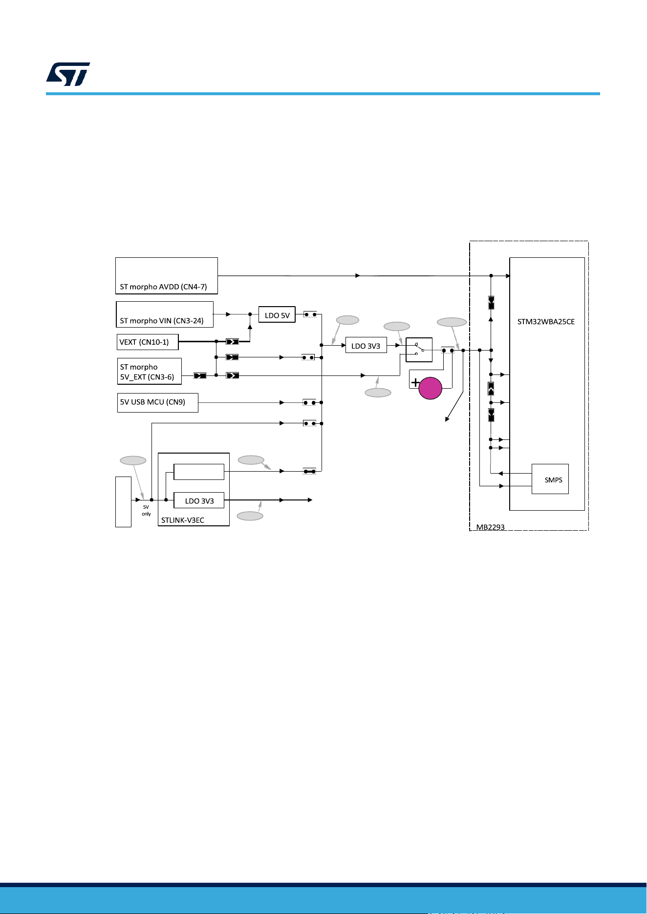
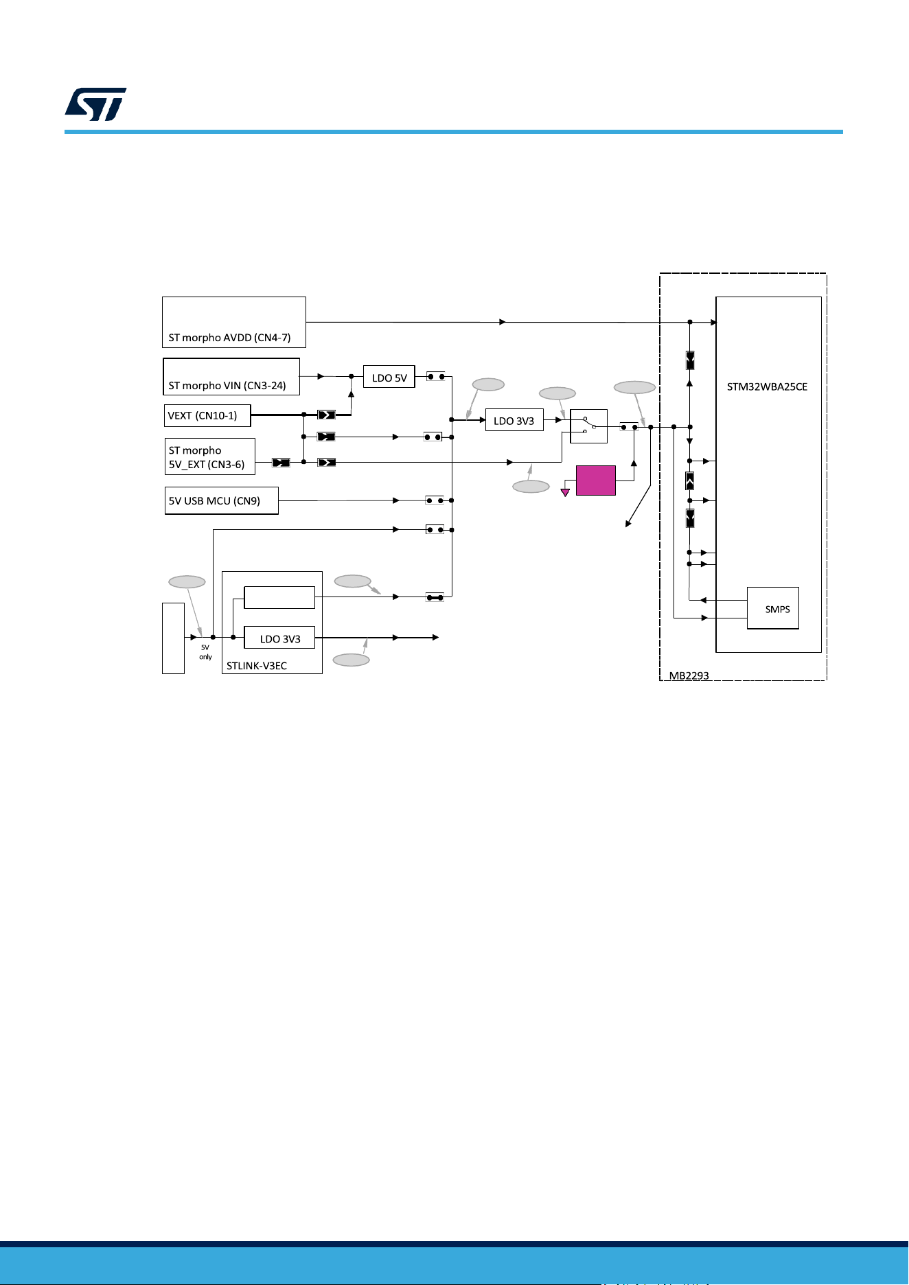
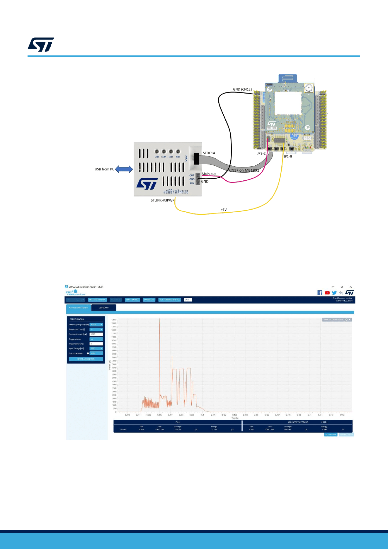
3. If it is necessary to do power consumption measurement during debugging, STMicroelectronics has an
interesting solution. It is possible to use STLINK-V3PWR. This product allows two sources of supply: a first for the
current measurement on the STM32WBA25CE, and a second for the rest of the board, such as LEDs. Like in the
previous case, the jumper (JP2) must be removed, and the main supply for the current measurement is
connected to pin 2 of JP2 (refer to Figure 10). For the second source (+5V), remove the jumper on JP1 and
connect this source to the top side (pin 1, 3, 5, 7, or 9 of JP1).
The supply voltage must be between 1.8 and 3.3 V. AVDD input must not be used, and SB1 must be ON during
this measurement.
Figure 10. Current measurement with STLINK-V3PWR
The details above concern the supply of the board by STLINK-V3PWR. Now, the debug feature of these tools
also needs some modification.
By default, MB2293 is delivered without the possibility of debugging by an external tool. Nevertheless, it is
possible to solder an MIPI-10 connector on the CN3 footprint.
For more details, refer to Section 7.13: MIPI-10 interface and pinout
Caution:
By default, this 10
‑
pin MIPI connector (CN3) is not assembled because it prohibits the use of an ARDUINO
®
shield. The height of the connector is not compatible with the plug of the ARDUINO
®
shield. Moreover, it is
always possible to plug an ST morpho shield on the bottom side of MB1801.
STM32WBA25CE
JP1[5-6]
5V
VDD
3V3
JP1[7-8]
1V8 to 3V3
JP1[3-4]
JP1[9-10]
+5Vaux
Level shifter (WBA side)
STLINK-V3PWR
VBUS_STLK
5V_STLK
JP1[1-2]
Power switch
Level shifter (ST-LINK side)
5V
only
STLINK-V3
3V3_STLK
MB2293
ST morpho
5V_EXT (CN3-6)
VEXT(CN10-1)
LDO 5V
LDO 3V3
5V USB MCU CN9)
LDO 3V3
ARDUINO
®
VIN (CN5-8)
ST morpho VIN (CN3-24)
AVDD (CN11-1)
ARDUINO
®
AVDD (CN6-8)
ST morpho AVDD (CN4-7)
SMPS
USB STLNK
DT59624V1
UMxxxx
Hardware layout and configuration
UMxxxx - Draft
page 19/48
Figure 11. Configuration for current measurement with STLINK-V3PWR
Caution: No VCP is available on the MIPI10 connector (CN17). If you need VCP1, replace connector CN17 with a 14
‑
pin
STDC14 connector.
After connection, download STM32CubeMonitor-Power (STM32CubeMonPwr) from the www.st.com website and
install it. This software allows the user to carry out dynamic current measurements with ease. Figure 12 shows an
example of a current measurement (firmware: Heart Rate from the STM32CubeWBA firmware package).
Figure 12. Example of current measurement with an external STLINK-V3PWR
For more details on using STLINK-V3PWR, a dedicated page is available on the www.st.com website.
UMxxxx
Hardware layout and configuration
UMxxxx - Draft
page 20/48
7.2
Radio output configuration
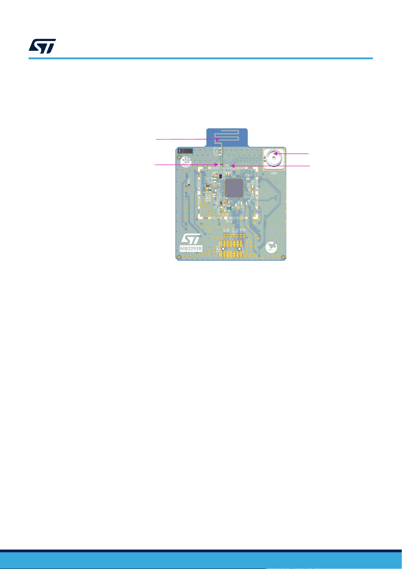
• By default, the board is configured with R1 ON and R2 OFF to use the PCB antenna.
• The configuration to use the SMA antenna is R1 OFF and R2 ON. The user must assemble the SMA
connector which is not present by default.
Figure 13. Antenna elements on MCU RF board
Printed circuit antenna
SMA connector
R1
R2
7.3
Clock sources
7.3.1
HSE clock references
The accuracy of the high‑speed clock (HSE) of the MCU RF board is committed to a 32 MHz crystal oscillator.
The HSE oscillator is trimmed during board manufacturing.
7.3.2
LSE clock references
The accuracy of the low‑speed clock (LSE) of the MCU RF board is committed to a 32.768 kHz crystal oscillator.
DT59649V1
UMxxxx
Hardware layout and configuration
UMxxxx - Draft
page 21/48
7.4
Reset sources
The reset signal of NUCLEO-WBA25CE1 is active LOW. The internal PU forces the RST signal to a high
level. The sources of reset are:
• Reset push-button (B4)
• Embedded STLINK-V3EC
• ARDUINO
®
connector (CN5 pin 3), reset from the ARDUINO
®
board
• ST morpho connector (CN3 pin 14)
7.5
Embedded STLINK-V3EC
The STLINK-V3EC programming and debugging tool is integrated into NUCLEO-WBA25CE1.
Features supported on STLINK-V3EC:
• USB 2.0 full-speed interface
• Probe firmware update through USB
• JTAG communication support up to 21 MHz
• SWD and SWV communication support up to 24 MHz
• 3.0 to 3.6 V application voltage support and 5 V tolerant inputs
• Virtual COM port (VCP) up to 16 Mbps
• Optional drag-and-drop flash memory programming binary files
• Multipath bridge USB to SPI/UART/I
2
C/GPIOs
• Status COM LED (LD5) which blinks during communication with the PC (red by default)
• Fault LED (LD6) alerting on USB overcurrent (green, orange, or red)
• USB-C
®
overvoltage protection (U10) with current limitation
For detailed information about the STLINK-V3EC capabilities such as LED management, drivers, and firmware,
refer to the technical note Overview of ST-LINK derivatives (TN1235) at www.st.com.
For information about the debugging and programming features of STLINK-V3EC, refer to the user manual
STLINK-V3SET debugger/programmer for STM8 and STM32 (UM2448) at www.st.com.
7.5.1
Drivers
STLINK-V3EC requires a dedicated USB driver, which, for Windows 7
®
and Windows 8
®
is available from
www.st.com. For Windows 10
®
, it is not necessary to install the driver. ST-LINK is automatically identified.
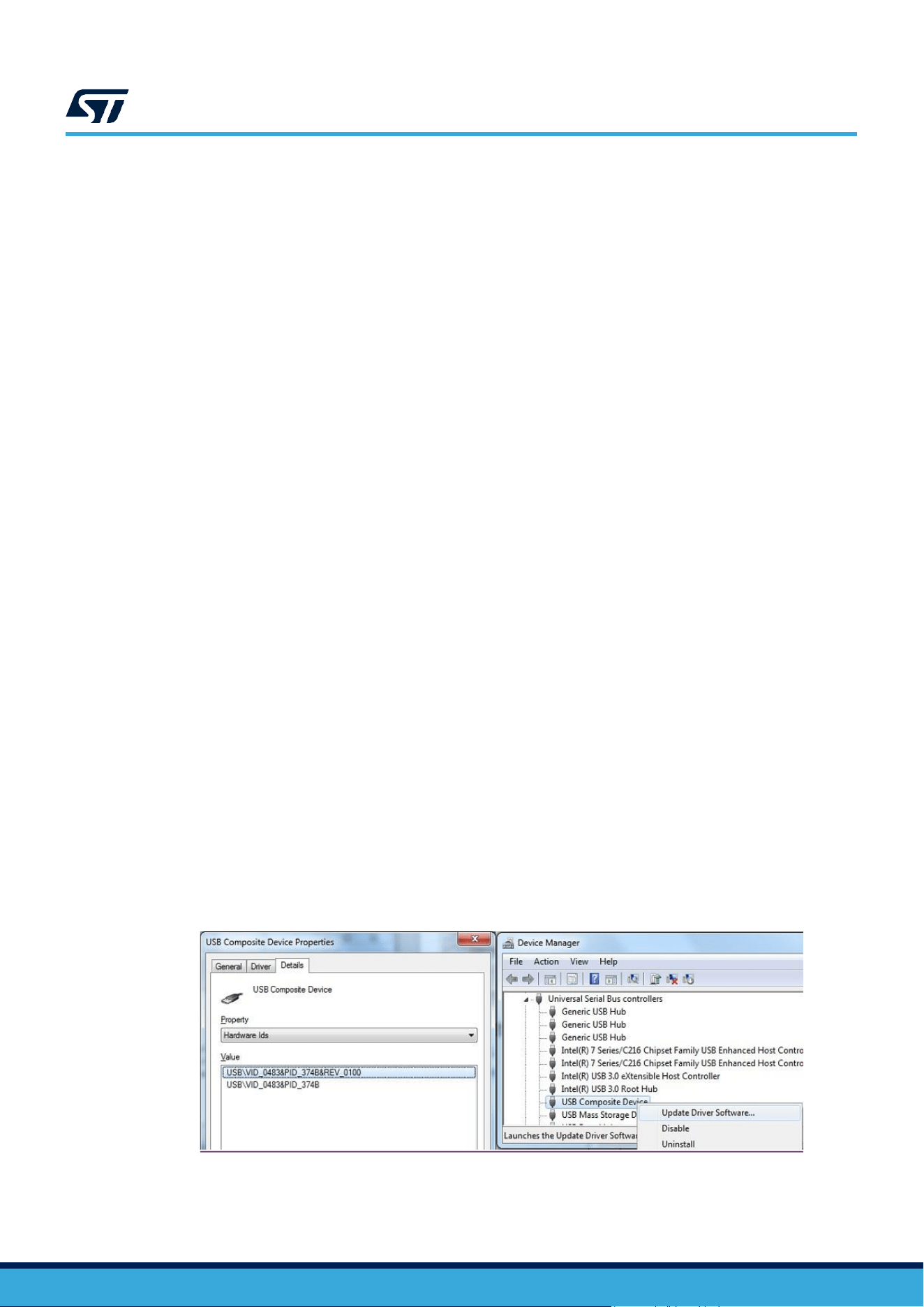
In case the NUCLEO-WBA25CE1 board is connected to the PC before the driver is installed, some board interfaces
might be declared as Unknown in the PC device manager. In this case, the user must install the dedicated driver
files and update the driver of the connected device from the device manager, as shown in Figure 14. USB
composite device.
Note: It is preferable to use the USB Composite Device to handle a full recovery.
Figure 14. USB composite device
UMxxxx
Hardware layout and configuration
UMxxxx - Draft
page 22/48
7.5.2 STLINK-V3EC firmware upgrade
STLINK-V3EC embeds a firmware mechanism (STSW-LINK007) for the in‑place upgrade through the USB port.
The firmware might evolve during the lifetime of the STLINK-V3EC product (for example new functionalities, bug
fixes, support for new microcontroller families). Visit the www.st.com website before starting to use the NUCLEO-
WBA25CE1 board, then periodically to stay updated with the latest firmware version.
For detailed information on the ST-LINK USB drivers, refer to the technical note Overview of ST-LINK derivatives
(TN1235) at www.st.com.
7.5.3 STLINK-V3EC USB connector (CN15)
The main function of this connector is the access to STLINK-V3EC embedded on the NUCLEO-WBA25CE1 for
the debugging as explained above. It allows supplying the board (refer to Section 7.1: Power supply). The
connector is a standard USB Type-C
®
connector.
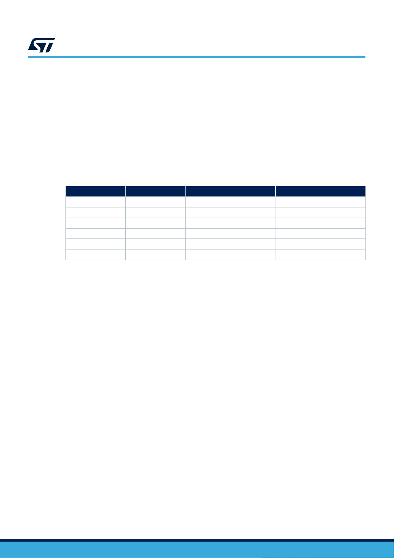
Table 5. STLINK-V3EC USB Type-C
®
connector (CN15)
Pin
Pin name
Signal name
Function
A4, A9, B4, B9
VBUS
VBUS_STLK
VBUS power
A7, B7
DM
STLK_USB_N
DM
A6, B6
DP
STLK_USB_P
DP
A5
CC1
-
Configuration Channel-
B5
CC2
-
Configuration Channel-
A1, A12, B1, B12
GND
GND
GND
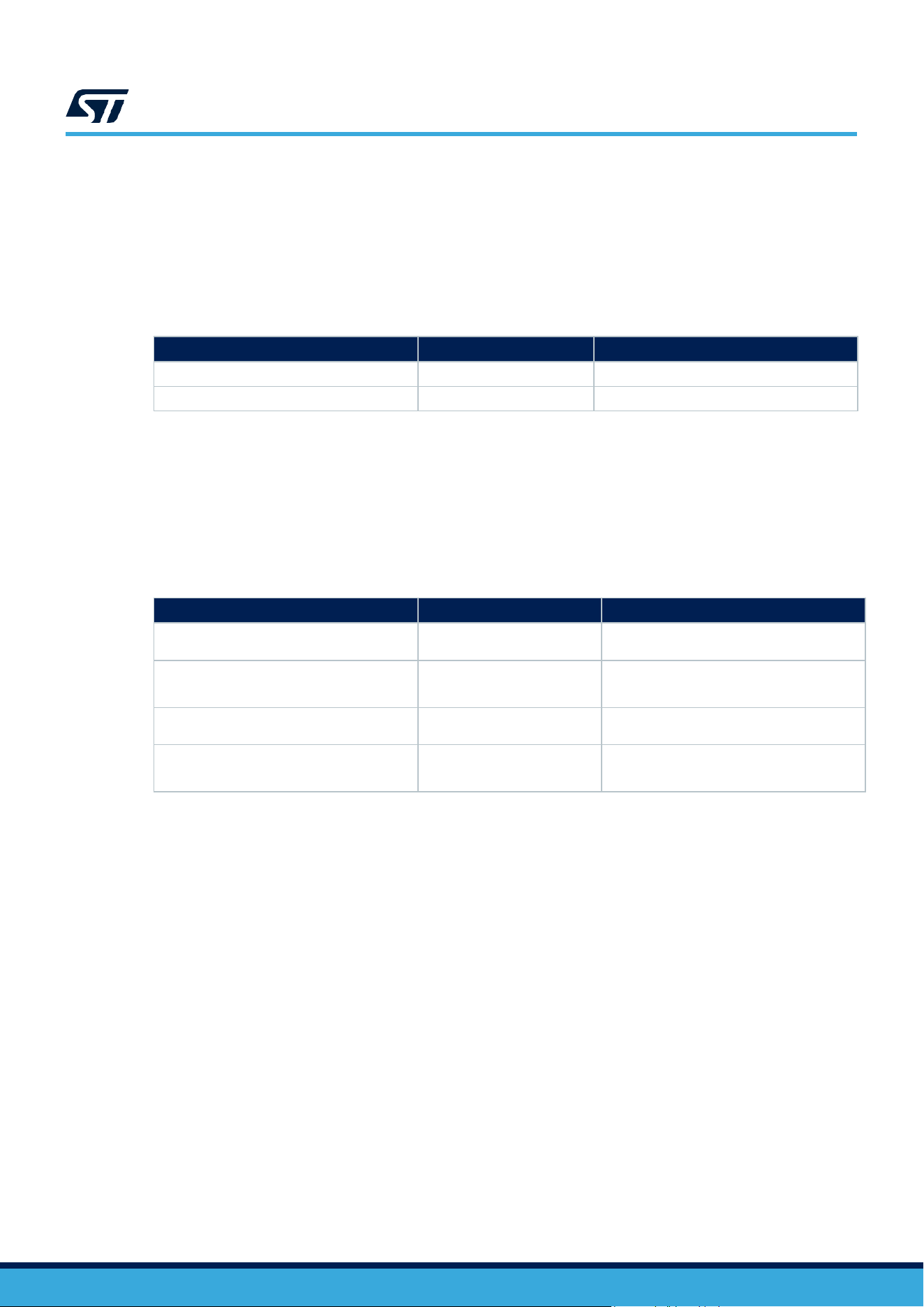
UMxxxx
Hardware layout and configuration
UMxxxx - Draft
page 23/48
7.5.4 Virtual COM port USART1 (VCP1)
STLINK-V3EC offers a USB Virtual COM port bridge. This feature allows access to the USART1 of NUCLEO-
WBA25CE1 by the USB ST-LINK connector. By default, this USART1 interface of NUCLEO-WBA25CE1 is
connected to the VCP1 of the STLINK-V3EC MCU (STM32F723IE).
Access is possible on the CN3 connector of the mezzanine board (MB1801). Both signals Tx and Rx are
available, and two solder bridges allow disconnecting them of the UART coming from the SoC. By default, VCP1
is connected to the USART1 of STM32WBA25CE.
Table 6. VCP1 interface pinout description
STM32WBA25CE (MB2293)
CN3 (MB1801)
STM32F723IE (MB1801)
USART1 Rx (PA12/pin 28)
Pin 35 (GPIO23) (SB5 ON)
STLK_VCP_TX: PG14/pin A7
USART1 Tx (PA6/pin 7) (SB21 ON)
Pin 37 (GPIO24) (SB3 ON)
STLK_VCP_RX: PG9/pin C10
7.5.5 Virtual COM port USART (VCP2)
It is possible to replace the mass storage interface with a second Virtual COM port. It is also necessary to do a
firmware upgrade through STM32CubeProgrammer (refer to the technical note Overview of ST-LINK derivatives
(TN1235) at www.st.com.
The access is possible on the CN3 and CN4 connectors of the mezzanine board (MB1801). All signals (Tx, Rx,
RTS, and CTS) are available. SB4 needs to be connected to use PA15 as RTS.
Table 7. VCP2 interface pinout description
STM32WBA25CE (MB2293)
CN3 and CN4 (MB1801)
STM32F723IE (MB1801)
LPUART1_RX (PA1)
SB10 ON and SB4 OFF by default
CN4/pin 37 (GPIO55) (SB7 ON)
T_VCP2_TX : PC10/pin B14
LPUART1_TX (PH3)
SB8 ON and SB43 OFF by default
CN4/pin 35 (GPIO54) (SB8 ON)
T_VCP2_RX : PB11/pin R13
LPUART1_CTS(PB15)
SB16 OFF and SB38 OFF by default
CN4/pin26 (GPIO46) (SB25 ON)
T_VCP2_RTS : PD12/pin N13
LPUART1_RTS (PA10)
SB35 OFF by default
CN3/pin2 (GPIO2) (SB23 ON)
T_VCP2_CTS : PD11/pin N14
7.5.6
Level shifter
NUCLEO-WBA25CE1 features a system to supply STM32WBA25CE with a voltage different from the ST-LINK
one. 3V3 sources always supply ST-LINK. By default, the same voltage value supplies STM32WBA25CE and ST-
LINK, but it is possible to supply the SoC with another value. It accepts voltage between 1.8 and 3.3 V trust to a
specific component (level shifter). This level shifter ensures the voltage conversion between ST-LINK and the
SoC. It drives SWD and UART signals connected to the VCP1 or VCP2 on the ST-LINK.
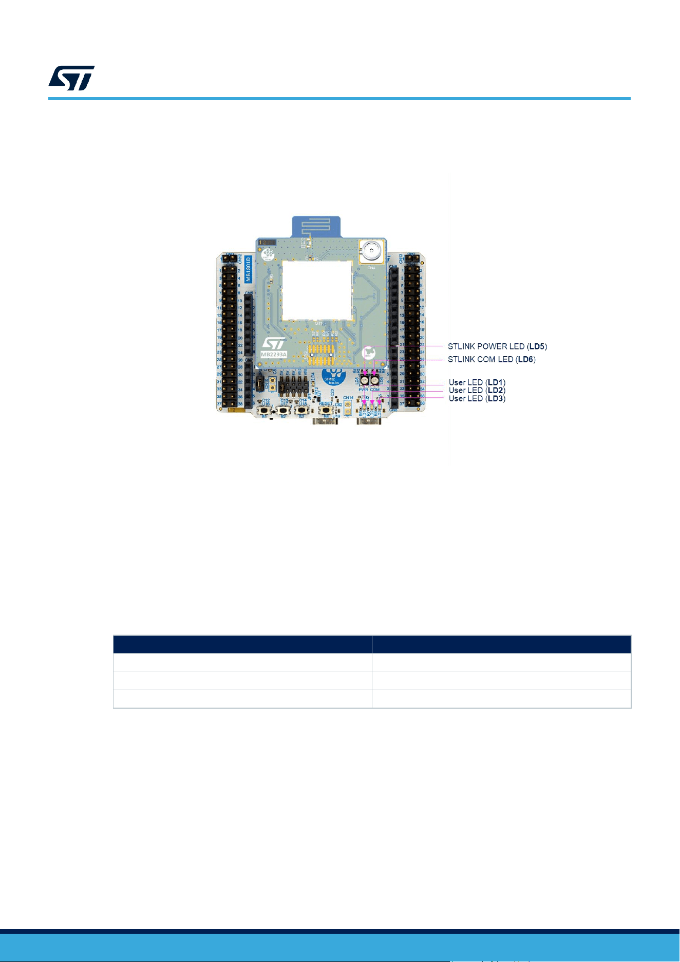
UMxxxx
Hardware layout and configuration
UMxxxx - Draft
page 24/48
7.6
LEDs
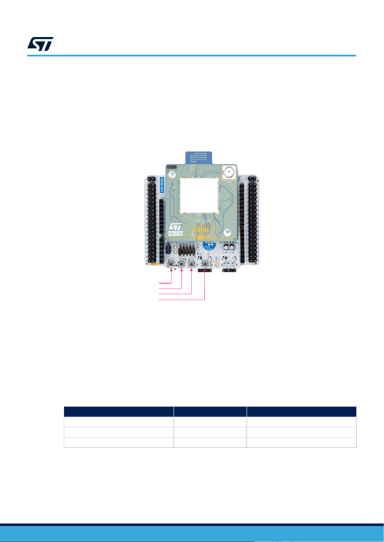
Four LEDs on the top side of the Nucleo board help the user during the application development.
Figure 15. LEDs location
• LD1: This blue LED is available for user application.
• LD2: This green LED is available for user application.
• LD3: This red LED is available for user application.
• LD4: This LED turns green when a 5V source is available (to select the 5V source, refer to
Section 7.1.3: 5 V power supply).
• LD5: This LED gives information about the STLINK-V3EC target power.
• LD6: This LED blinks during communication with the PC.
For detailed information about the STLINK-V3EC LEDs, refer to the technical note Overview of ST-LINK
derivatives (TN1235) at www.st.com.
Table 8. I/O configuration for the physical user interface
Name
I/O
User LED (LD1)
PA7
User LED (LD2)
PB12
User LED (LD3)
PB15
UMxxxx
Hardware layout and configuration
UMxxxx - Draft
page 25/48
7.7
Push-buttons
7.7.1
Description
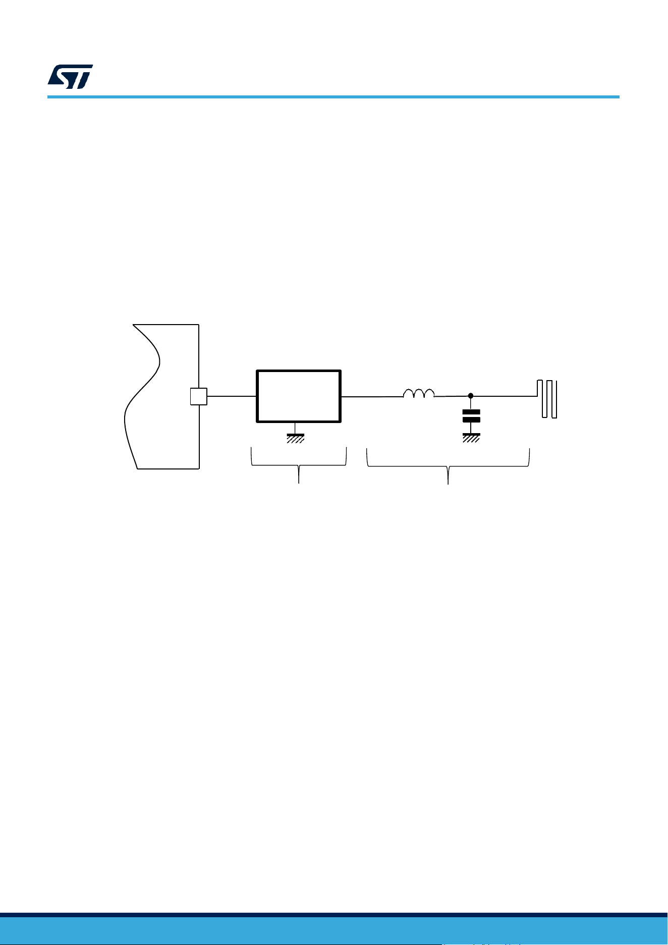
NUCLEO-WBA25CE1 provides two types of buttons:
• USER1 push-button (B1)
• USER2 push-button (B2)
• USER2 push-button (B3)
• Reset push-button (B4), used to reset the Nucleo board
Figure 16. Push-button location
User push-button (B1)
User push-button (B2)
User push-button (B3)
Reset push-button (B4)
7.7.2
Reset push-button
B4 is dedicated to the hardware reset of the Nucleo board.
7.7.3
User push-buttons
There are three push buttons available for the user application. They are connected to PA1, PA2 and PC13. It is
possible to use with GPIO reading or to wake up the device.
Note that PC13 is also connected to ARDUINO
®
and ST morpho connectors as GPIO, depending on the use
case that can generate conflict with B2. In this case, it is possible to remove the connection of B2 (SB4 OFF).
Table 9. I/O configuration for the physical user interface
Name
I/O
Wake-Up available
USER1 push-button (B1)
PA1
WKUP3
USER2 push-button (B2)
PC13
WKUP2
USER3 push-button (B3)
PA2
WKUP4
DT59627V1
UMxxxx
Hardware layout and configuration
UMxxxx - Draft
page 26/48
52
IPD
C1
1.1 pF
7.8
RF I/O stage
Due to FCC/ISED constraints, the antenna cannot be removable. So, the board is proposed by default with a PCB
antenna. This antenna is described in the application note Guidelines for meander design using low-cost PCB
antennae with 2.4 GHz radio for STM32WB/WB0 MCUs (AN5129) available at www.st.com. Between the
STM32WBA25CE and the antenna, there is an integrated passive device (IPD). This IPD considerably reduces
harmonics and adapts the output to 50 Ω. This makes it easy to pass certification requirements, such as FCC,
ISED, RED, and MIC. At the IPD output, there are two passive components for antenna matching.
The harmonics are drastically reduced with this IPD.
The antenna matching network is built with two components L3 and C1. This guarantees a comfortable margin in
all cases. The study considers the drift of the components (accuracy and temperature), the drift due to the PCB,
and the variation of STM32WBA25CE. Of course, depending on the component manufacturer and the
specification of the PCB, these component values can change after optimization.
Figure 17. RF I/O stage
STM32WBA25CE
L3
PCB
antenna
Integrated passive device
Matching network of the
PCB antenna
DT59369V1
1.5 nH
UMxxxx
Hardware layout and configuration
UMxxxx - Draft
page 27/48
MB2293
®
MB1801
7.9
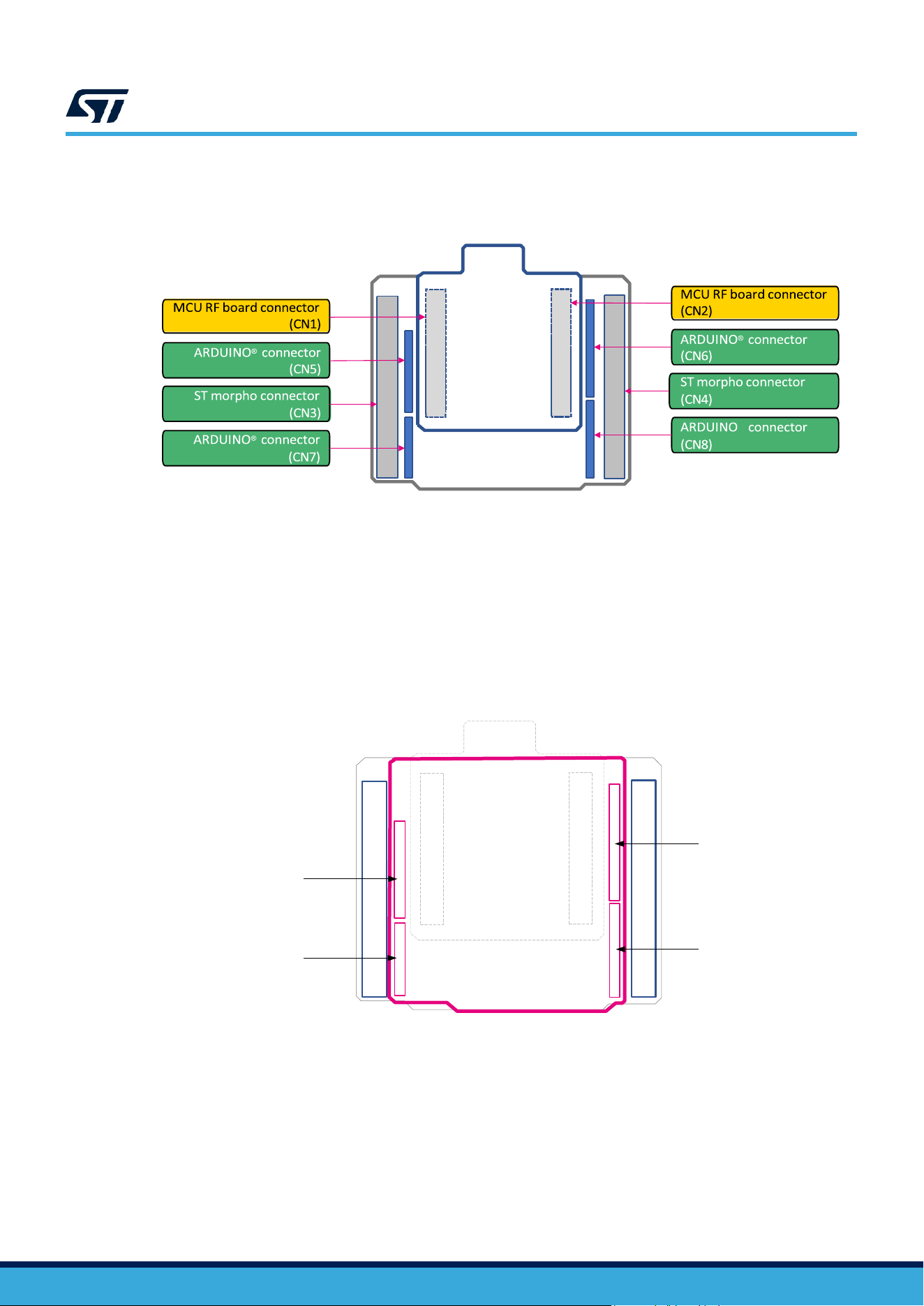
Connector naming
Figure 18. Connector locations and namings
interface and pinout
7.10.1
Description
On the bottom side of the board, there is an ARDUINO
®
Uno V3 extension socket. It is built around four standard
connectors (CN5, CN6, CN7, and CN8). Most shields designed for ARDUINO
®
can fit with the Discovery kits to
offer flexibility in small form factor applications.
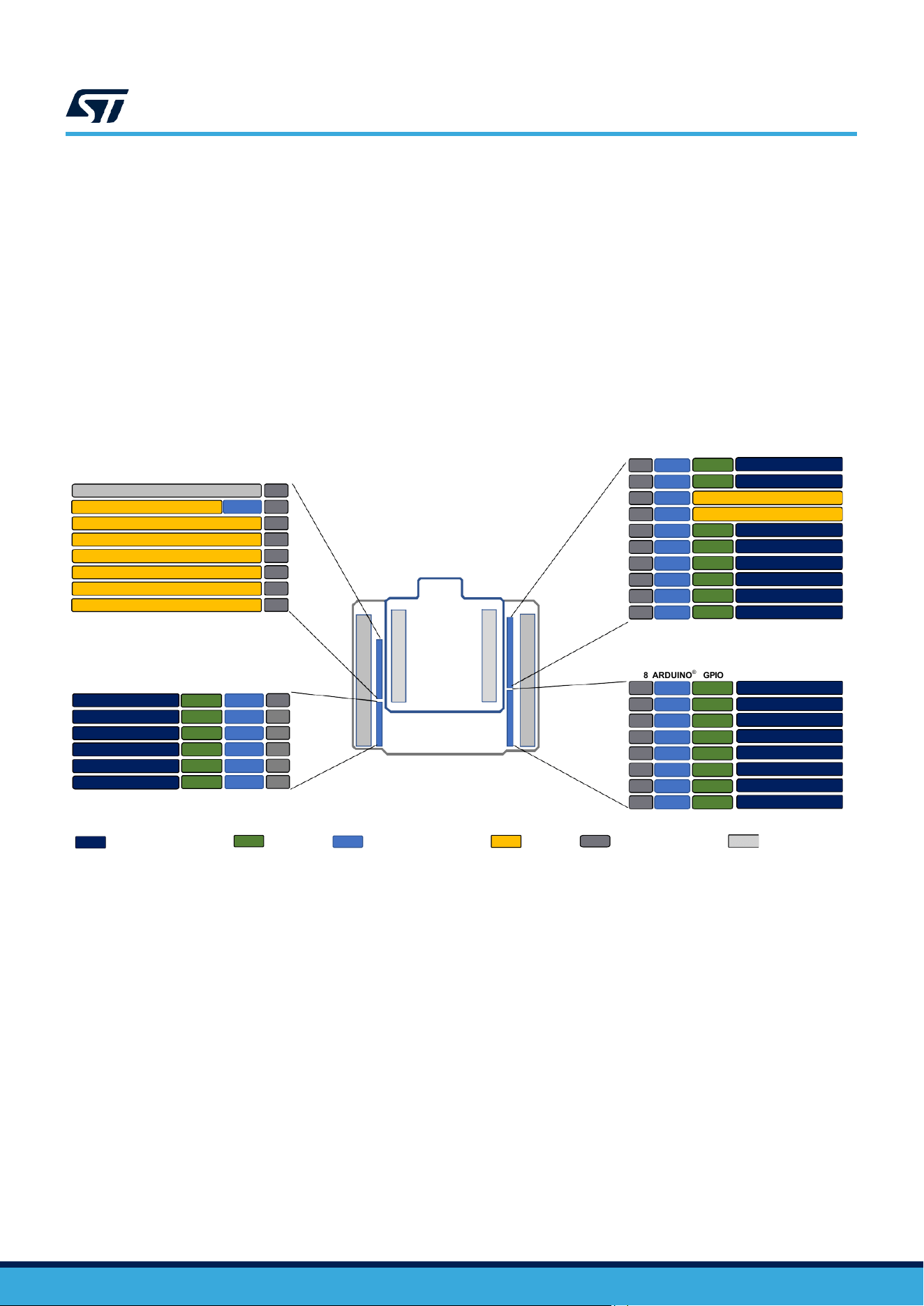
Figure 19. ARDUINO
®
Uno connectors and ARDUINO
®
shield location
ARDUINO
®
Digital 8-15
(CN6)
ARDUINO
®
Power
(CN5)
ARDUINO
®
Analog 0-5
(CN7)
ARDUINO
®
(CN8)
Digital 0-7
NC
IOREF
NRST
3V3
5V
GND
GND
VIN
D15
D14
AVDD
GND
D13
D12
D11
D10
D9
D8
A0
A1
A2
A3
A4
A5
D7
D6
D5
D4
D3
D2
D1
D0
ARDUINO® Uno shield
DT59630V1
DT59629V1
7.10
ARDUINO
®
UMxxxx
Hardware layout and configuration
UMxxxx - Draft
page 28/48
ARDUINO
®
CN5
nc
1
Vtarget
IOREF
2
NRST
3
3V3 4
5V 5
GND 6
GND 7
VIN 8
CN8 ARDUINO
®
GPIO
STM32WBA25CE
PA7
PA1
PA2
PA5
PA8
PA6
GPIO ARDUINO
®
CN7
GPIO11
A0
1
STM32WBA25CE
8
D7 GPIO42 PA11
7
D6
GPIO44
PA7
D5
GPIO47
PA8
D4 GPIO49
PA9
D3 GPIO50
PB12
D2 GPIO52
PC13
D1 GPIO54
PA6 (VCP2_TX*)
D0 GPIO55
PA12 (VCP2_RX*)
7.10.2
Operating voltage
The ARDUINO
®
Uno V3 connectors support 5 V, 3.3 V, and VDD for I/O compatibility.
Caution:
Do not supply 3.3 or 5 V from the ARDUINO
®
shield. Supplying 3.3 or 5 V from the ARDUINO
®
shield might
damage the Nucleo board.
The Nucleo board can be supplied by the ARDUINO
®
connector. A dedicated pin is available. VIN allows
supplying the board directly. To use this feature, refer to Section 7.1.2: 7 to 12 V power supply.
7.10.3
ARDUINO
®
pinout
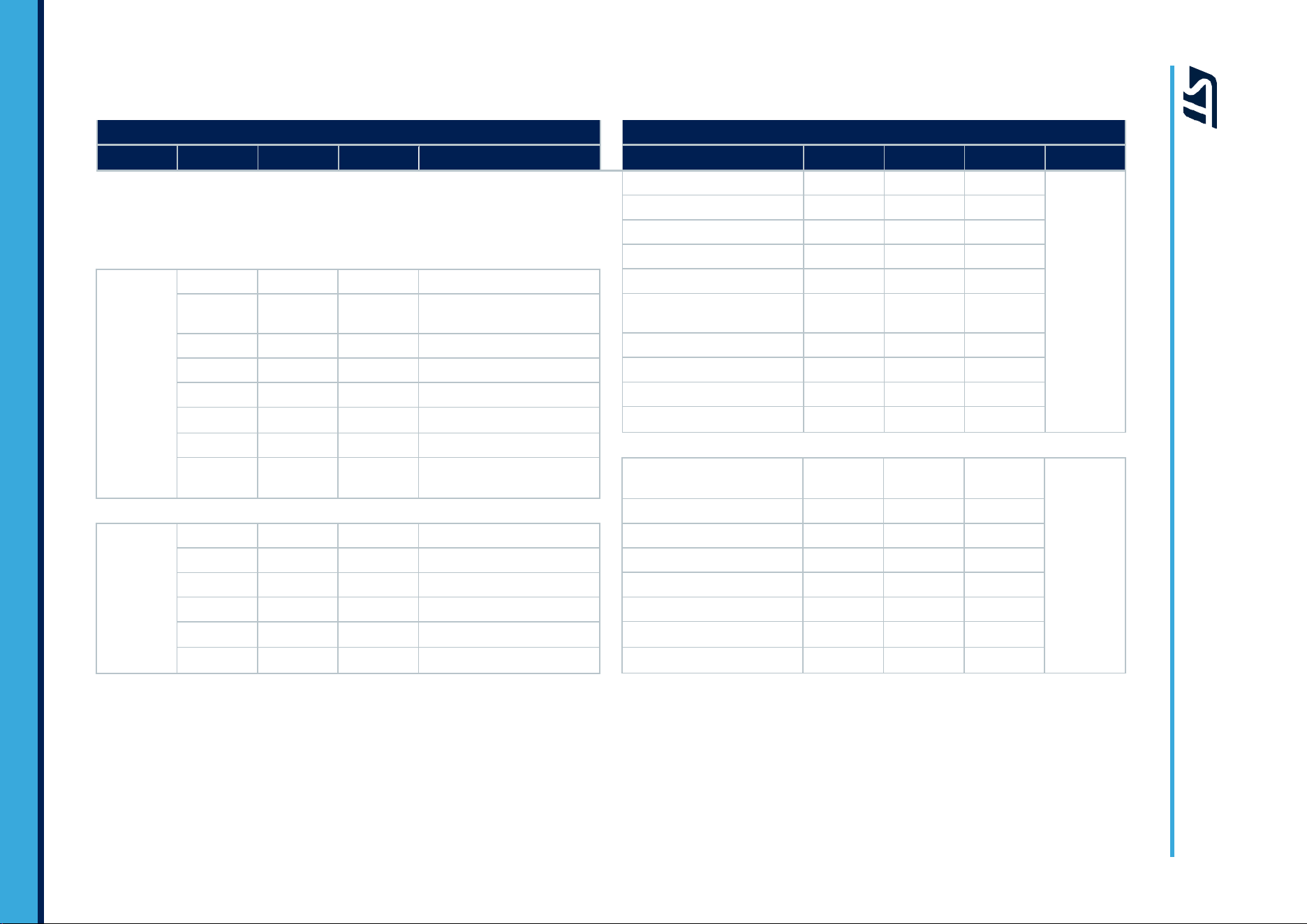
Figure 18 shows the position of the ARDUINO
®
shield when plugged into NUCLEO-WBA25CE1. The pinout
shown in Figure 20 corresponds to standard ARDUINO
®
naming. To see the correspondence with the STM32,
refer to Table 10.
Figure 20. ARDUINO
®
connector pinout
CN6 ARDUINO
®
GPIO
STM32WBA25CE
GPIO12
A1
2
6
GPIO17
A2
3
5
GPIO18
A3
4
4
GPIO21
A4
5
3
GPIO22
A5
6
(*) Optional, need to change
2
state of solder bridges
1
STM32WBA25CE pin name
GPIO number ARDUINO
®
signal name Power ARDUINO
®
pin number Not connected (nc)
DT59631V1
ARDUINO
®
10
D15
GPIO28
PB2
connector description
9
D14
GPIO29
PA11
8
AVDD
VDDA
7
GND
GND
6
D13
GPIO31
PA8
5
D12
GPIO33
PA10
4
D11
GPIO34
PA9
3
D10
GPIO37
PA5
2
D9
GPIO39
PA6
1
D8
GPIO41
PB2
CN7
1
A0
PA7
ADC4_IN2
2
A1
PA1
ADC4_IN8
3
A2
PA2
ADC4_IN7
4
A3
PA5
ADC4_IN4
5
A4
PA8
ADC4_IN1
6
A5
PA6
ADC4_IN3
GPIO
PA11
D7
8
CN8
GPIO/TIM2_CH3
PA7
D6
7
GPIO/TIM2_CH2
PA8
D5
6
GPIO
PA9
D4
5
GPIO/TIM2_CH1
PB12
D3
4
GPIO
PC13
D2
3
USART1_TX
(1)
PA6/PH3
D1
2
USART1_RX
(1)
PA12 / PA1
D0
1
Table 10. Pinout of the ARDUINO
®
connectors
Left connectors
Right connectors
Connector
Pin number
Pin name
MCU pin
Function
Function
MCU pin
Pin name
Pin number
Connector
I2C1_SCL/I2C3_SCL
PB2
D15
10
I2C1_SDA/I2C3_SDA
PA11
D14
9
VDDA
-
AVDD
8
GND
-
GND
7
1 NC - NC (reserved for tests)
SPI3_SCK
PA8
D13
6
2 3V3 - IOREF
SPI3_MISO
PA10
D12
5
CN6
(IOREF)
3 NRST NRST NRST
SPI3_MOSI
PA9
D11
4
3V3 - 3V3
SPI3_NSS/TIM2_CH1
PA5
D10
3
CN5
GPIO/TIM2_CH4
PA6
D9
2
5 5V - 5V
6 GND - GND
GPIO
PB2
D8
1
1.
Optional, need to change the state of solder bridges.
UM3448
Hardware layout and configuration
UM3448 - Rev 1
page 29/48
7
GND
-
GND
8
VIN
-
External supply input
(+12Vmax)
UMxxxx
Hardware layout and configuration
UMxxx - Draft
page 30/48
nc GPIO0
nc
GPIO1
VDD
1
3
5
2
GPIO2
4
GPIO4
PA10*
nc
PD5
GPIO26
PB2 GPIO28 D15
6
5V_EXT
PA11 GPIO29
D14
1 2 GPIO25
nc
3 4 GPIO27
nc
5 6
GPIO30 PA7 (LD1)
interface and pinout
7.11.1
Description
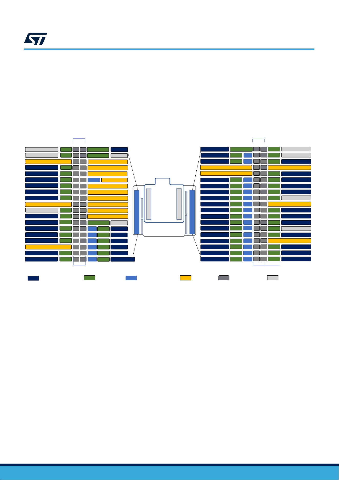
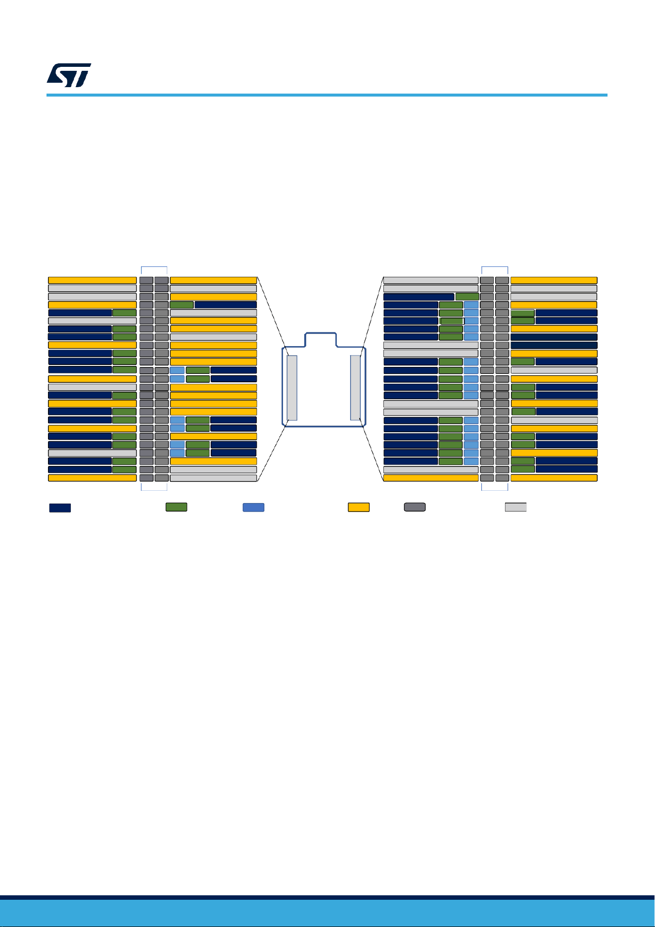
The ST morpho connectors (CN3 and CN4) are male pin headers accessible on both sides of the board. All
signals and power pins of the MCU are available on the ST morpho connectors. An oscilloscope, logical analyzer,
or voltmeter can also probe these connectors.
pinout
Figure 21. ST morpho pinout
ST morpho
ST morpho
connectors description
STM32WBA25CE
GPIO
ST morpho
GPIO
STM32WBA25CE
PH3 (BOOT0)
GPIO3
7
8
GND
VDDA
7
8
5V_USB_MCU
PA13 (JTMS/SWDIO)
GPIO5
9
10
5V-INT
GND
9
10 GPIO32
nc
PA14(JTCLK/SWCLK)
GPIO6
11
12
IOREF
Vtarget
PA8
GPIO31
D13
11
12 GPIO35 PB8 (USB_FS_P)
nc
GPIO8
13
14
NRST
PA10 GPIO33
D12
13
14
GPIO36 PB9 (USB_FS_N)
nc
GPIO9
15
16
3V3
PA9
GPIO34
D11
15
16
GPIO38 PB15 (LPUART_CTS)
nc
GPIO10
17
18
5V
PA5
GPIO37
D10
17
18 GPIO40
nc
GND
19
20
GND
PA6
GPIO39
D9
19
20 GND
nc
GPIO13
21
22
GND
PB2 GPIO41
D8
21
22
GPIO43
nc
PB12 (LD2)
GPIO14
23
24
VIN
PA11 GPIO42
D7
23
24 GPIO45 nc
PC14 (OSC32_IN) *
GPIO15
25
26
GPIO7
nc
PA7
GPIO44
D6
25
26
GPIO46 nc
PC15 (OSC32_OUT) *
GPIO16
27
28
A0
GPIO11 PA7
PA8
GPIO47
D5
27
28
GPIO48
PB15 (LPUART_CTS)
NC
GPIO19
29
30
A1
GPIO12 PA1
PA9 GPIO49
D4
29
30
GPIO51 PC13 (B2)
NC
GPIO20
31
32
A2
GPIO17 PA2
PB12 GPIO50
D3
31
32 GND
VBAT
33
34
A3 GPIO18 PA5
PC13
GPIO52
D2
33
34 GPIO53 PA2 (B3)
PA12 (VCP1_RX)
GPIO23
35
36
A4
GPIO21 PA8
PH3 (VCP2_TX*) GPIO54
D1
35
36 GPIO56 PA1 (B1)
PA6 (VCP1_TX) GPIO24
37
38
A5
GPIO22
PA6
(*) Optional, need to change
state of solder bridges
PA1 (VCP2_RX*)
GPIO55
D0
37
38 GPIO57
PB15 (LD3)
STM32WBA25CE pin name
GPIO number ARDUINO
®
signal name Power ST morpho pin number Not connected (nc)
CN3
CN4
DT59632V1
7.11
ST morpho
7.11.2
ST morpho
UMxxxx
Hardware layout and configuration
UMxxx - Draft
page 31/48
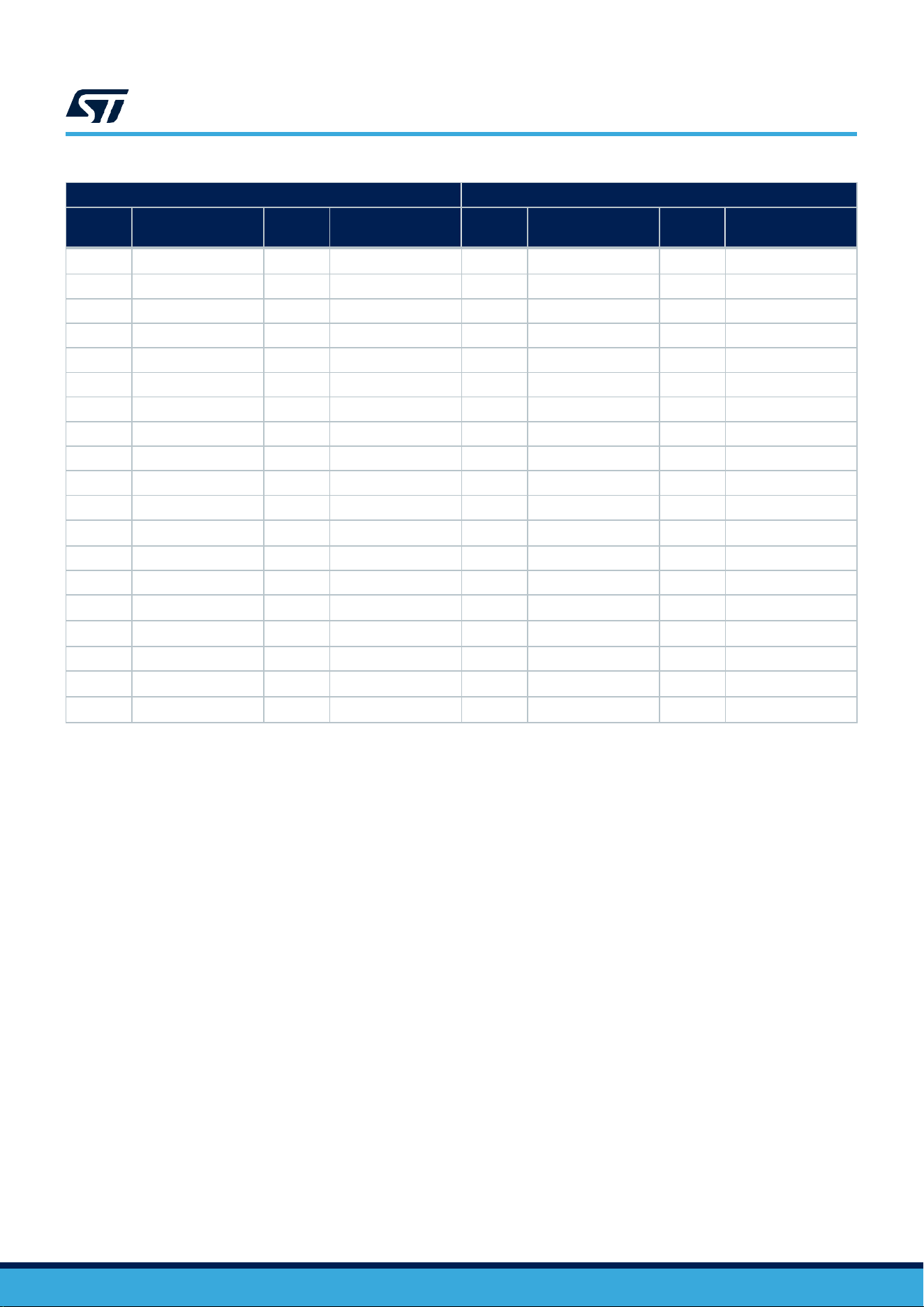
Table 11. ST morpho pinout
CN3
CN4
Pin
number
STM32WBA25CE pin
name
Pin
number
STM32WBA25CE pin
name
Pin
number
STM32WBA25CE pin
name
Pin
number
STM32WBA25CE pin
name
1
NC
2
PA10
1
NC
2
NC
3
NC
4
NC
3
PB2
4
NC
5
VDD
6
5V_EXT
5
PA11
6
PA7
7
BOOT0
8
GND
7
VDDA
8
5V_USB_MCU
9
PA13
10
NC
9
GND
10
NC
11
PA14
12
IOREF
11
PA8
12
PB8 (USB_FS_P)
13
NC
14
NRST
13
PA10
14
PB9 (USB_FS_N)
15
NC
16
3V3
15
PA9
16
PB15
17
NC
18
5V
17
PA5
18
NC
19
GND
20
GND
19
PA6
20
GND
21
NC
22
GND
21
PB2
22
NC
23
PC4
24
VIN
23
PA11
24
NC
25
PC14
26
NC
25
PA7
26
PB15
27
PC15
28
PA7NC
27
PA8
28
NC
29
NC
30
PA1
29
PA9
30
PC13
31
NC
32
PA2
31
PB12
32
GND
33
VBAT
34
PA5
33
PC13
34
PA2
35
PA12
36
PA8
35
PH3 (VCP2_TX)
(1)
36
PA1
37
PA6
38
PA6
37
PA1 (VCP2_RX)
(1)
38
PB15
1.
Optional, need to change the state of solder bridges.
UMxxxx
Hardware layout and configuration
UMxxx - Draft
page 32/48
MCU RF board
connectors description
MCU RF board
5
interface and pinout
7.12.1
Description
The MCU RF board connectors (CN1 and CN2) are accessible on the top side of the board. They are used to
plug the MCU RF board into the mezzanine board.
pinout
Figure 22. MCU RF board connector pinout
CN1
MCU RF board
CN2
GND
1
2
VDD1
NC
1
2
GND
NC
3
4
NC
NC
3
4
NC
NC
5
6
GND
NC
GPIO26
5
6
NC
GND
7
8
GPIO2
PA10
PB2 GPIO28
D15
7
8
GND
PH3 (BOOT0)
GPIO3
9
10
NC
PA11 GPIO29
D14
9
10
GPIO30
PA7 (LD1)
NC
11
12
NRST
PA8 GPIO31
D13
11
12
GPIO32
NC
PA13 (JTMS/SWDIO)
GPIO5
13
14
GND
PA10 GPIO33
D12
13
14
GND
PA14 (JTCLK/SWCLK)
GPIO6
15
16
NC
P9 GPIO34
D11
15
16
USB_FS_P
GND
17
18
VDD3
NC
17
18
USB_FS_N
NC
GPIO8
19
20
VDDA
NC
19
20
GND
NC
GPIO9
21
22
GND
PA5 GPIO37 D10
21
22
GPIO38
PB15
NC
GPIO10
23
24
A0 GPIO11 PA7
PA6 GPIO39 D9
23
24
NC
GND
25
26
A1 GPIO12 PA1
PB2
GPIO41 D8
25
26
GND
NC
27
28
GND
PA11 GPIO42 D7
27
28
GPIO43
NC
PB12
GPIO14
29
30
VDD4
PA7 GPIO44 D6
29
30
GPIO45
NC
GND
31
32
VDD5
NC
31
32
GND
PC14 (OSC32_IN)
GPIO15
33
34
GND
NC
33
34
GPIO46
PB15
PC15 (OSC32_OUT)
GPIO16
35
36
A2 GPIO17 PA2
PA8 GPIO47
D5
35
36
NC
GND
37
38
A3 GPIO18 PA5
PA9 GPIO49 D4
37
38
GND
NC
GPIO19
39
40
GND
PB12 GPIO50 D3
39
40
GPIO51
PC13 (B2)
NC
GPIO20
41
42
A4 GPIO21
PA8
PC13
GPIO52 D2
41
42
GPIO53
PA2 (B3)
NC
43
44
A5 GPIO22 PA6
PH3 (VCP2_TX*) GPIO54 D1
43
44
GND
PA12 (VCP1_RX)
GPIO23
45
46
GND
PA1 (VCP2_RX*) GPIO55
D0
45
46
GPIO56
PA1 (B1)
PA6 (VCP1_TX)
GPIO24
47
48
VDD_QSPI
(*) Optional, need to change
NC
47
48
GPIO57
PB15 (LD3)
GND
49
50
VDDUSB
state of solder bridges
NC
49
50
GND
STM32WBA25CE pin name
GPIO number ARDUINO
®
signal name Power ST morpho pin number Not connected (nc)
DT59633V1
7.12
MCU RF board
7.12.2
MCU RF board
UMxxxx
Hardware layout and configuration
UMxxx - Draft
page 33/48
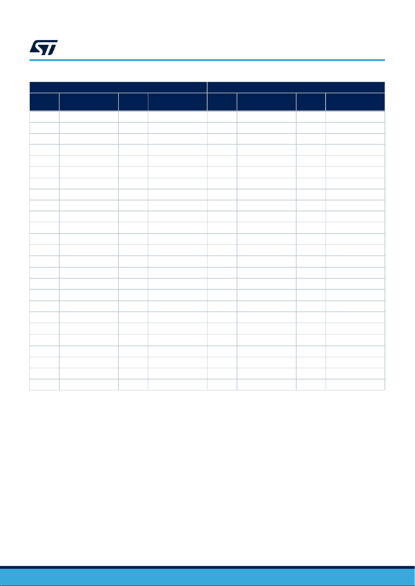
Table 12. MCU RF board connector pinout
CN1
CN2
Pin
number
STM32WBA25CE pin
name
Pin
number
STM32WBA25CE pin
name
Pin
number
STM32WBA25CE pin
name
Pin
number
STM32WBA25CE pin
name
1
GND
2
VDD1
1
NC
2
GND
3
NC
4
NC
3
NC
4
NC
5
NC
6
GND
5
NC
6
NC
7
GND
8
PA10
7
PB2
8
GND
9
BOOT0
10
NC
9
PA11
10
PA7
11
NC
12
NRST
11
PA8
12
NC
13
PA13
14
GND
13
PA10
14
GND
15
PA14
16
NC
15
PA9
16
PB8
17
GND
18
VDD3
17
NC
18
PB9
19
NC
20
VDDA
19
NC
20
GND
21
NC
22
GND
21
PA5
22
PB15
23
NC
24
PA7
23
PA6
24
NC
25
GND
26
PA1
25
PB2
26
GND
27
NC
28
GND
27
PA11
28
NC
29
PB12
30
VDD4
29
PA7
30
NC
31
GND
32
VDD5
31
NC
32
GND
33
PC14
34
GND
33
NC
34
PB15
35
PC15
36
PA2
35
PA8
36
NC
37
GND
38
PA5
37
PA9
38
GND
39
NC
40
GND
39
PB12
40
PC13
41
NC
42
PA8
41
PC13
42
PA2
43
NC
44
PA6
43
PH3
44
GND
45
PA12
46
GND
45
PA1
46
PA1
47
PA6
48
VDD_QSPI
47
NC
48
PB15
49
GND
50
VDDUSB
49
NC
50
GND
1. Optional, need to change the state of solder bridges.
UMxxxx
Hardware layout and configuration
UMxxx - Draft
page 34/48
7.13
MIPI10 connector
7.13.1
Description
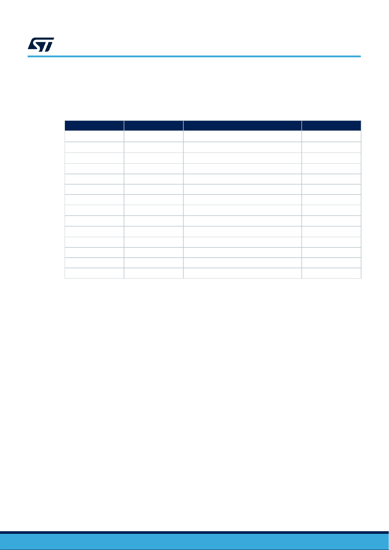
On the MCU RF board, there is a footprint for direct debugging (SWD). The footprint is compatible with MIPI10
connector (CN3). By default, CN3 is not assembled.
When using CN3, the resistors R5, R6, R7, R8, and R9 must be connected.
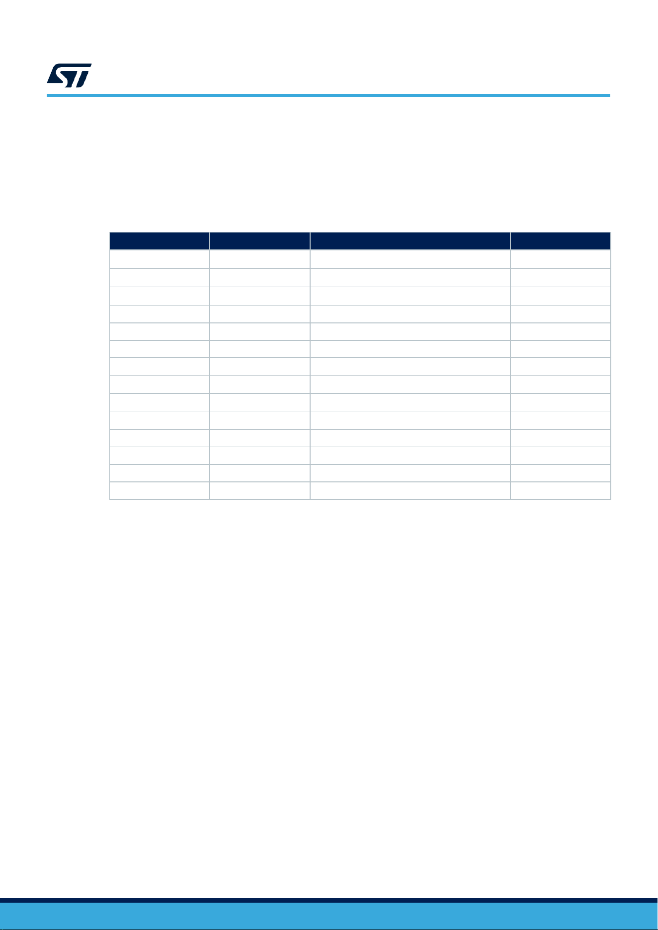
Table 13. Pinout of the MIPI10/STDC14 connector (CN3 of the MCU RF board)
STDC14 pin #
MIPI10 pin #
Pin description
Type
1
-
Reserved
(1)
-
2
-
Reserved
(1)
-
3
1
T_VCC
(2)
I
4
2
T_JTMS/T_SWDIO
I/O
5
3
GND
S
6
4
T_JCLK/T_SWCLK
O
7
5
GND
S
8
-
-
I
9
7
T_JCLK
O
10
-
-
O
11
9
GNDDetect
O
12
10
T_NRST
O
13
-
T_VCP_RX
O
14
-
T_VCP_TX
I
UMxxxx
Hardware layout and configuration
UMxxx - Draft
page 35/48
connector
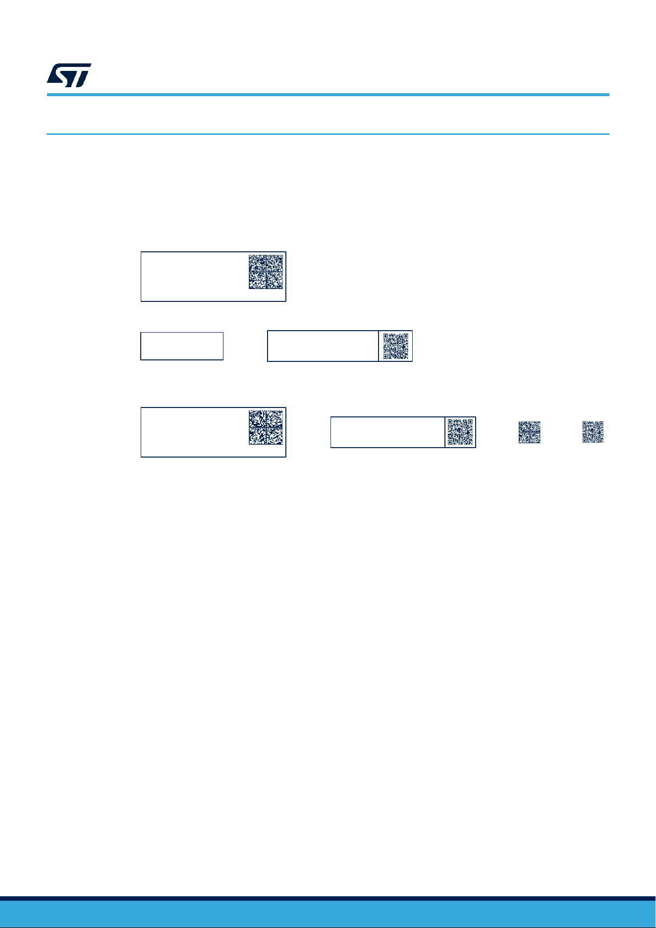
On the mezzanine board, there is also a connector (CN17) for direct debugging. This connector is compatible
with MIPI10 and it is possible to change the connector or connect the missing signals to have STDC14 full
signals. Nevertheless, it is necessary to put the onboard ST-LINK in reset mode by mounting JP3.
Table 14. Pinout of the MIPI10/STDC14 connector (CN3 of the MCU RF board)
STDC14 pin #
MIPI10 pin #
Pin description
Type
1
-
Reserved
(1)
-
2
-
Reserved
(1)
-
3
1
T_VCC
(2)
I
4
2
T_JTMS/T_SWDIO
I/O
5
3
GND
S
6
4
T_JCLK/T_SWCLK
O
7
5
GND
S
8
6
T_JTDO/T_SWO
(3)
I
9
7
T_JCLK
O
10
8
T_JTDI/NC
(4)
O
11
9
GNDDetect
O
12
10
T_NRST
O
13
-
T_VCP_RX
O
14
-
T_VCP_TX
I
1. Do not connect to the target.
2. Input for STLINK-V3EC
3. SWO is optional, required only for Serial Wire Viewer (SWV)
4. NC means it is not required for the SWD connection.
7.14
MIPI10
UMxxx
NUCLEO-WBA25CE1 product
information
UM3448 - Rev 1
page 36/48
MBxxxx-Variant-yzz
syywwxxxxx
Product order code
Product identification
syywwxxxxx
MBxxxx-Variant-yzz
8
NUCLEO-WBA25CE1 product information
8.1
Product marking
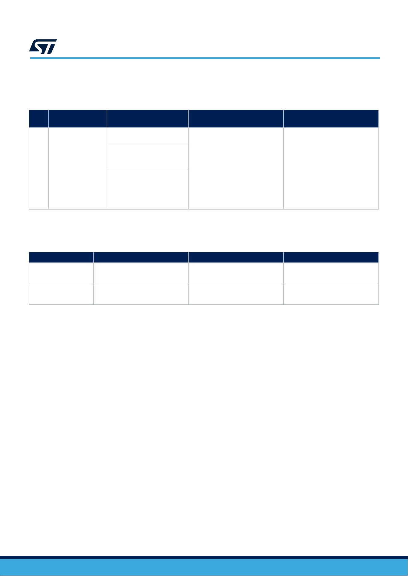
The product and each board composing the product are identified with one or several stickers. The stickers,
located on the top or bottom side of each PCB, provide product information:
• Main board featuring the target device: product order code, product identification, serial number, and board reference
with revision.
Single-sticker example:
Dual-sticker example:
and
• Other boards if any: board reference with revision and serial number.
Examples:
or or or
On the main board sticker, the first line provides the product order code, and the second line the product
identification.
On all board stickers, the line formatted as “MBxxxx-Variant-yzz” shows the board reference “MBxxxx”, the
mounting variant “Variant” when several exist (optional), the PCB revision “y”, and the assembly revision “zz”, for
example B01. The other line shows the board serial number used for traceability.
Products and parts labeled as “ES” or “E” are not yet qualified or feature devices that are not yet qualified.
STMicroelectronics disclaims any responsibility for consequences arising from their use. Under no circumstances
will STMicroelectronics be liable for the customer's use of these engineering samples. Before deciding to use
these engineering samples for qualification activities, contact STMicroelectronics' quality department.
“ES” or “E” marking examples of location:
• On the targeted STM32 that is soldered on the board (for an illustration of STM32 marking, refer to the
STM32 datasheet Package information paragraph at the www.st.com website).
• Next to the ordering part number of the evaluation tool that is stuck, or silk-screen printed on the board.
Some boards feature a specific STM32 device version, which allows the operation of any bundled commercial
stack/library available. This STM32 device shows a “U” marking option at the end of the standard part number
and is not available for sales.
To use the same commercial stack in their applications, the developers might need to purchase a part number
specific to this stack/library. The price of those part numbers includes the stack/library royalties.
MBxxxx-Variant-yzz
syywwxxxxx
syywwxxxxx
MBxxxx-Variant-yzz
Product order code
Product identification
UMxxx
NUCLEO-WBA25CE1 product
information
UM3448 - Rev 1
page 37/48
8.2
NUCLEO-WBA25CE1 product
history
Table 15. Product history
Order
code
Product
identification
Product details
Product change description
Product limitations
NUCLEO
-WBA25CE1
MCU: STM32WBA25CEU7
silicon revision "TBC"
MCU errata sheet:
STM32WBA2xxx device errata
ENUWBA25CE1$CR2
(TBC)
Initial revision
No limitation
Boards:
• MB1801-USB-D01
(mezzanine board)
• MB2293-WBA2-B05
(MCU RF board)
8.3
Board revision history
Table 16. Board revision history
Board reference
Board variant and revision
Board change description
Board limitations
MB1801
(mezzanine board)
USB-D01
Initial revision
No limitation
MB2293
(MCU RF board)
WBA2-B05
Initial revision
No limitation

UMxxxx
Product disposal
UM3448 - Rev 1
page 38/48
9 Federal Communications Commission (FCC) and ISED Canada
Compliance Statements
9.1 FCC Compliance Statement
Identification of products: NUCLEO-WBA25CE1
FCC ID: YCP-MB229300
Radio Frequency (RF) Exposure Compliance of Radio communication: To satisfy FCC RF Exposure
requirements, a separation distance of 20cm or more should be maintained between the antenna of this
device and persons during operation. To ensure compliance, operation at a closer distance than this is
not recommended. This transmitter must not be co-located or operating in conjunction with any other
antenna or transmitter.
Part 15.19
This device complies with Part 15 of the FCC Rules. Operation is subject to the following two conditions:
(1) this device may not cause harmful interference, and (2) this device must accept any interference
received, including interference that may cause undesired operation.
Part 15.21
Any changes or modifications to this equipment not expressly approved by STMicroelectronics may cause
harmful interference and void the user's authority to operate this equipment. Part 15.105 This equipment
has been tested and found to comply with the limits for a Class B digital device, pursuant to part 15 of the
FCC Rules. These limits are designed to provide reasonable protection against harmful interference in a
residential installation. This equipment generates uses and can radiate radio frequency energy and, if not
installed and used in accordance with the instruction, may cause harmful interference to radio
communications. However, there is no guarantee that interference will not occur in a particular installation.
If this equipment does cause harmful interference to radio or television reception which can be
determined by turning the equipment off and on, the user is encouraged to try to correct interference by
one or more of the following measures:
- Reorient or relocate the receiving antenna.
- Increase the separation between the equipment and receiver.
- Connect the equipment into an outlet on circuit different from that to which the receiver is connected.
- Consult the dealer or an experienced radio/TV technician for help.
Responsible party (in the USA)
Francesco Doddo
STMicroelectronics, Inc.
200 Summit Drive | Suite 405 | Burlington, MA 01803
USA
Telephone: +1 781-472-9634
9.2 ISED Compliance Statement
Identification of products: NUCLEO-WBA25CE1
IC: 8976A-MB229300
Identification du produit : NUCLEO-WBA25CE1
Contient sous-ensemble certifié IC : 8976A-MB229300
Compliance Statement
Notice: This device complies with ISED Canada licence-exempt RSS standard(s). Operation is subject to
the following two conditions: (1) this device may not cause interference, and (2) this device must accept
any interference, including interference that may cause undesired operation of the device.

UMxxxx
Product disposal
UM3448 - Rev 1
page 39/48
Déclaration de conformité
Avis: Le présent appareil est conforme aux CNR d'ISDE Canada applicables aux appareils radio exempts
de licence. L'exploitation est autorisée aux deux conditions suivantes : (1) l'appareil ne doit pas produire
de brouillage, et (2) l'utilisateur de l'appareil doit accepter tout brouillage radioélectrique subi, même si le
brouillage est susceptible d'en compromettre le fonctionnement.
RF exposure statement
This device complies with ISED radiation exposure limits set forth for general population. This device must
be installed to provide a separation distance of at least 20cm from all persons and must not be co-located
or operating in conjunction with any other antenna or transmitter. Le présent appareil est conforme aux
niveaux limites d’exigences d’exposition RF aux personnes définies par ISDE. L’appareil doit être installé
afin d’offrir une distance de séparation d’au moins 20cm avec les personnes et ne doit pas être installé à
proximité ou être utilisé en conjonction avec une autre antenne ou un autre émetteur.
10 RED Compliance Statement
Déclaration de conformité CE simplifiée
STMicroelectronics déclare que l'équipement radioélectrique du type "NUCLEO-WBA25CE1" est
conforme à la directive 2014/53/UE.
Bande de fréquence utilisée en transmission et puissance maximale rayonnée dans cette bande :
• Bande de fréquence : 2400-2483.5 MHz (Bluetooth®)
• Puissance maximale : 8 mW p.i.r.e
Simplified EC compliance statement
Hereby, STMicroelectronics declares that the radio equipment type "NUCLEO-WBA25CE1” is in
compliance with Directive 2014/53/EU.
Frequency range used in transmission and maximal radiated power in this range:
• Frequency range: 2400-2483.5 MHz (Bluetooth®)
• Maximal power: 8 mW e.i.r.p

UMxxxx
Product disposal
UM3448 - Rev 1
page 40/48
UMxxxx
Product disposal
UM3448 - Rev 1
page 41/48
11
Product disposal
Disposal of this product: WEEE (Waste Electrical and Electronic Equipment)
(Applicable in Europe)
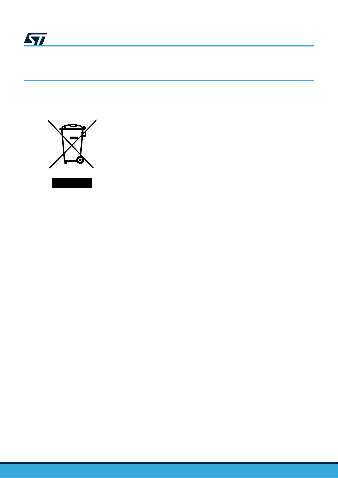
This symbol on the product, accessories, or accompanying documents indicates that the
product and its electronic accessories should not be disposed of with household waste at the
end of their working life.
To prevent possible harm to the environment and human health from uncontrolled waste
disposal, please separate these items from other type of waste and recycle them responsibly
to the designated collection point to promote the sustainable reuse of material resources.
Household users:
You should contact either the retailer where you buy the product or your local authority for
further details of your nearest designated collection point.
Business users:
You should contact your dealer or supplier for further information.
UM3448
UM3448 - Rev 1
page 42/48
Revision history
Table 17. Document revision history
Date
Revision
Changes
11-Dec-2025
1
Initial release.

UM3448
Contents
UM3448 - Rev 1
page 43/48
Contents
1 Features ............................................................................................................................................. 2
2 Ordering information ...................................................................................................................... 3
2.1 Codification ........................................................................................................................................... 3
3 Development environment ............................................................................................................ 4
3.1 System requirements .......................................................................................................................... 4
3.2 Development toolchains ..................................................................................................................... 4
3.3 Demonstration software ...................................................................................................................... 4
3.4 CAD resources ..................................................................................................................................... 4
4 Conventions ...................................................................................................................................... 5
5 Safety recommendations ............................................................................................................... 6
5.1 Targeted audience ............................................................................................................................... 6
5.2 Handling the board .............................................................................................................................. 6
6 Quick start ......................................................................................................................................... 7
6.1 Getting started ...................................................................................................................................... 7
7 Hardware layout and configuration ............................................................................................ 8
7.1 Power supply ......................................................................................................................................13
7.1.1 General description .......................................................................................................................... 13
7.1.2 7 to 12 V power supply .................................................................................................................... 14
7.1.3 5 V power supply .............................................................................................................................. 14
7.1.4 Current measurement ...................................................................................................................... 16
7.2 Radio output configuration................................................................................................................20
7.3 Clock sources .....................................................................................................................................20
7.3.1 HSE clock references ...................................................................................................................... 20
7.3.2 LSE clock references ....................................................................................................................... 20
7.4 Reset sources .................................................................................................................................... 21
7.5 Embedded STLINK-V3EC ................................................................................................................ 21
7.5.1 Drivers ................................................................................................................................................ 21
7.5.2 STLINK-V3EC firmware upgrade ................................................................................................... 22
7.5.3 STLINK-V3EC USB connector (CN15) ......................................................................................... 22
7.5.4 Virtual COM port USART1 (VCP1) ................................................................................................ 23
7.5.5 Virtual COM port USART2 (VCP2) ................................................................................................ 23
7.5.6 Level shifter ....................................................................................................................................... 23
7.6 LEDs ....................................................................................................................................................24
7.7 Push-buttons ......................................................................................................................................25
7.7.1 Description ......................................................................................................................................... 25

UM3448
Contents
UM3448 - Rev 1
page 44/48
7.7.2 Reset push-button ........................................................................................................................... 25
7.7.3 User push-buttons ........................................................................................................................... 25
7.8 RF I/O stage ...................................................................................................................................... 26
7.9 Connector naming ............................................................................................................................ 27
7.10 ARDUINO
®
interface and pinout .................................................................................................... 27
7.10.1 Description ........................................................................................................................................ 27
7.10.2 Operating voltage ............................................................................................................................ 28
7.10.3 ARDUINO
®
pinout ........................................................................................................................... 28
7.11 ST morpho interface and pinout ..................................................................................................... 30
7.11.1 Description ........................................................................................................................................ 30
7.11.2 ST morpho pinout ............................................................................................................................ 30
7.12 MCU RF board interface and pinout .............................................................................................. 32
7.12.1 Description ........................................................................................................................................ 32
7.12.2 MCU RF board pinout ..................................................................................................................... 32
7.13 ETM 20 interface and pinout ........................................................................................................... 34
7.13.1 Description ........................................................................................................................................ 34
7.13.2 ETM 20 pinout ................................................................................................................................. 34
7.14 MIPI10 connector .............................................................................................................................. 35
8 NUCLEO-WBA25CE1 product information ............................................................................ 36
8.1 Product marking ................................................................................................................................ 36
8.2 NUCLEO-WBA25CE1 product history .......................................................................................... 37
8.3 Board revision history ....................................................................................................................... 37
9 Product disposal ........................................................................................................................... 42
Revision history ..................................................................................................................................... 43
List of tables ............................................................................................................................................ 46
List of figures .......................................................................................................................................... 47

UM3448
List of tables
UM3448 - Rev 1
page 45/48
List of tables
Table 1. List of available products ............................................................................................................................................................. 3
Table 2. Codification explanation............................................................................................................................................................... 3
Table 3. ON/OFF convention ..................................................................................................................................................................... 5
Table 4. Power supply selector (JP1) description ................................................................................................................................. 15
Table 5. STLINK-V3EC USB Type-C
®
connector (CN15) ................................................................................................................... 22
Table 6. VCP1 interface pinout description ............................................................................................................................................ 23
Table 7. VCP2 interface pinout description ............................................................................................................................................ 23
Table 8. I/O configuration for the physical user interface ..................................................................................................................... 24
Table 9. I/O configuration for the physical user interface ..................................................................................................................... 25
Table 10. Pinout of the ARDUINO
®
connectors ...................................................................................................................................... 29
Table 11. ST morpho pinout ....................................................................................................................................................................... 31
Table 12. MCU RF board connector pinout ............................................................................................................................................. 33
Table 13. MIPI10 pinout .............................................................................................................................................................................. 34
Table 14. Pinout of the MIPI10/STDC14 connector (CN3 of the MCU RF board) .............................................................................. 35
Table 15. Product history ............................................................................................................................................................................ 37
Table 16. Board revision history ................................................................................................................................................................ 37
Table 17. Document revision history ......................................................................................................................................................... 43

UM3448
List of figures
UM3448 - Rev 1
page 46/48
List of figures
Figure 1. NUCLEO-WBA25CE1 global view ......................................................................................................................................... 1
Figure 2. Hardware block diagram .......................................................................................................................................................... 8
Figure 3. NUCLEO-WBA25CE1 PCB top view ..................................................................................................................................... 9
Figure 4. NUCLEO-WBA25CE1 PCB bottom view of mezzanine board (MB1801) ...................................................................... 10
Figure 5. NUCLEO-WBA25CE1 (MB1801) mechanical dimensions (in millimeters) ..................................................................... 11
Figure 6. NUCLEO-WBA25CE1 (MB2293) mechanical dimensions (in millimeters) ..................................................................... 12
Figure 7. STM32WBA25CE power tree ............................................................................................................................................... 13
Figure 8. Current measurement with an ammeter .............................................................................................................................. 16
Figure 9. Current measurement with an external power supply ....................................................................................................... 17
Figure 10. Current measurement with STLINK-V3PWR ...................................................................................................................... 18
Figure 11. Configuration for current measurement with STLINK-V3PWR......................................................................................... 19
Figure 12. Example of current measurement with an external STLINK-V3PWR ............................................................................. 19
Figure 13. Antenna elements on MCU RF board ................................................................................................................................. 20
Figure 14. USB composite device ........................................................................................................................................................... 21
Figure 15. LEDs location .......................................................................................................................................................................... 24
Figure 16. Push-button location ............................................................................................................................................................... 25
Figure 17. RF I/O stage ............................................................................................................................................................................ 26
Figure 18. Connector locations and namings ........................................................................................................................................ 27
Figure 19. ARDUINO
®
Uno connectors and ARDUINO
®
shield location .......................................................................................... 27
Figure 20. ARDUINO
®
connector pinout ............................................................................................................................................... 28
Figure 21. ST morpho pinout ................................................................................................................................................................... 30
Figure 22. MCU RF board connector pinout .......................................................................................................................................... 32
Figure 23. MIPI10 footprint....................................................................................................................................................................... 34

UM3448
UM3448 - Rev 1
page 47/48
IMPORTANT NOTICE – READ CAREFULLY
STMicroelectronics NV and its subsidiaries (“ST”) reserve the right to make changes, corrections, enhancements, modifications, and improvements to ST
products and/or to this document at any time without notice. Purchasers should obtain the latest relevant information on ST products before placing orders. ST
products are sold pursuant to ST’s terms and conditions of sale in place at the time of order acknowledgment.
Purchasers are solely responsible for the choice, selection, and use of ST products and ST assumes no liability for application assistance or the design of
purchasers’ products.
No license, express or implied, to any intellectual property right is granted by ST herein.
Resale of ST products with provisions different from the information set forth herein shall void any warranty granted by ST for such product.
ST and the ST logo are trademarks of ST. For additional information about ST trademarks, refer to www.st.com/trademarks. All other product or service names
are the property of their respective owners.
Information in this document supersedes and replaces information previously supplied in any prior versions of this document.
© 2025 STMicroelectronics – All rights reserved

