Loading ...
Loading ...
Loading ...
65BDL3550Q
51
9.4. Dark Dot Defects
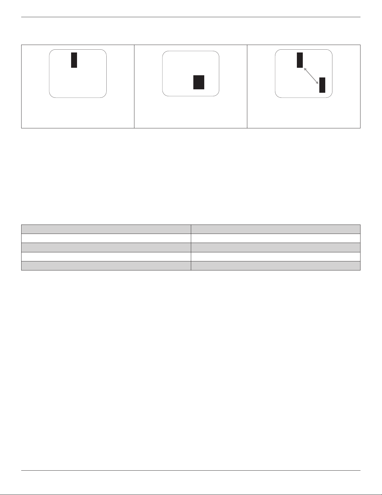
Black dot defects appear as pixels or sub-pixels that are always dark or “o”. These are the examples of black dot defects:
One dark dot Two adjacent dark dots = 1 pair of dark
dots
Two dark dots, specications denes
the minimum distance between dark
dots
9.5. Proximity of Pixel Defects
Because pixel and sub-pixels defects of the same type that are nearby one another may be more noticeable, Philips also
species tolerances for the proximity of pixel defects. In the table below you can nd specications about:
• Allowed amount of adjacent dark dots = (adjacent dark dots =1 pair of dark dots)
• Minimum distance between dark dots
• Total no. of all defective dots
9.6. Pixel Defect Tolerances
In order to qualify for repair due to pixel defects during the warranty period, a PDP / TFT panel in a Philips Plasma / LCD-
display must have pixel or sub-pixel defects exceeding the tolerances listed in the following table.
BRIGHT DOT EFFECT ACCEPTABLE LEVEL
1 lit sub pixel 2
BLACK DOT EFFECT ACCEPTABLE LEVEL
1 dark sub pixel 10
TOTAL DOT DEFECTS OF ALL TYPES 12
NOTE: * 1 or 2 adjacent sub pixel defects = 1 dot defect
9.7. MURA
Dark spots or patches may occasionally appear on some liquid crystal display (LCD) panels. This is known within the industry
as Mura, which is a Japanese term for “unevenness.” It is used to describe an irregular pattern or area in which uneven screen
uniformity appears under certain conditions. Mura is a result of the deterioration of the liquid crystal alignment layer and is most
commonly caused by long-term operation under high ambient temperatures. It is an industry- wide phenomenon and Mura is
not repairable. It is also not covered by our warranty terms.
Mura has been around since the introduction of LCD technology and with screens getting bigger and in operation 24/7, many
displays are running in low light conditions. This all adds to the possibility of Mura aecting displays.
HOW TO SPOT MURA
There are many symptoms of Mura and also multiple causes. Several of these are listed below:
• Impurities or foreign particles in the crystal matrix
• Uneven distribution of LCD matrix during manufacturing
• Non-uniform luminance distribution of the backlight
• Panel assembly induced stress
• Flaws within the LCD cells
• Thermal induced stress - high temperature operation over long periods of time
Loading ...
Loading ...
Loading ...