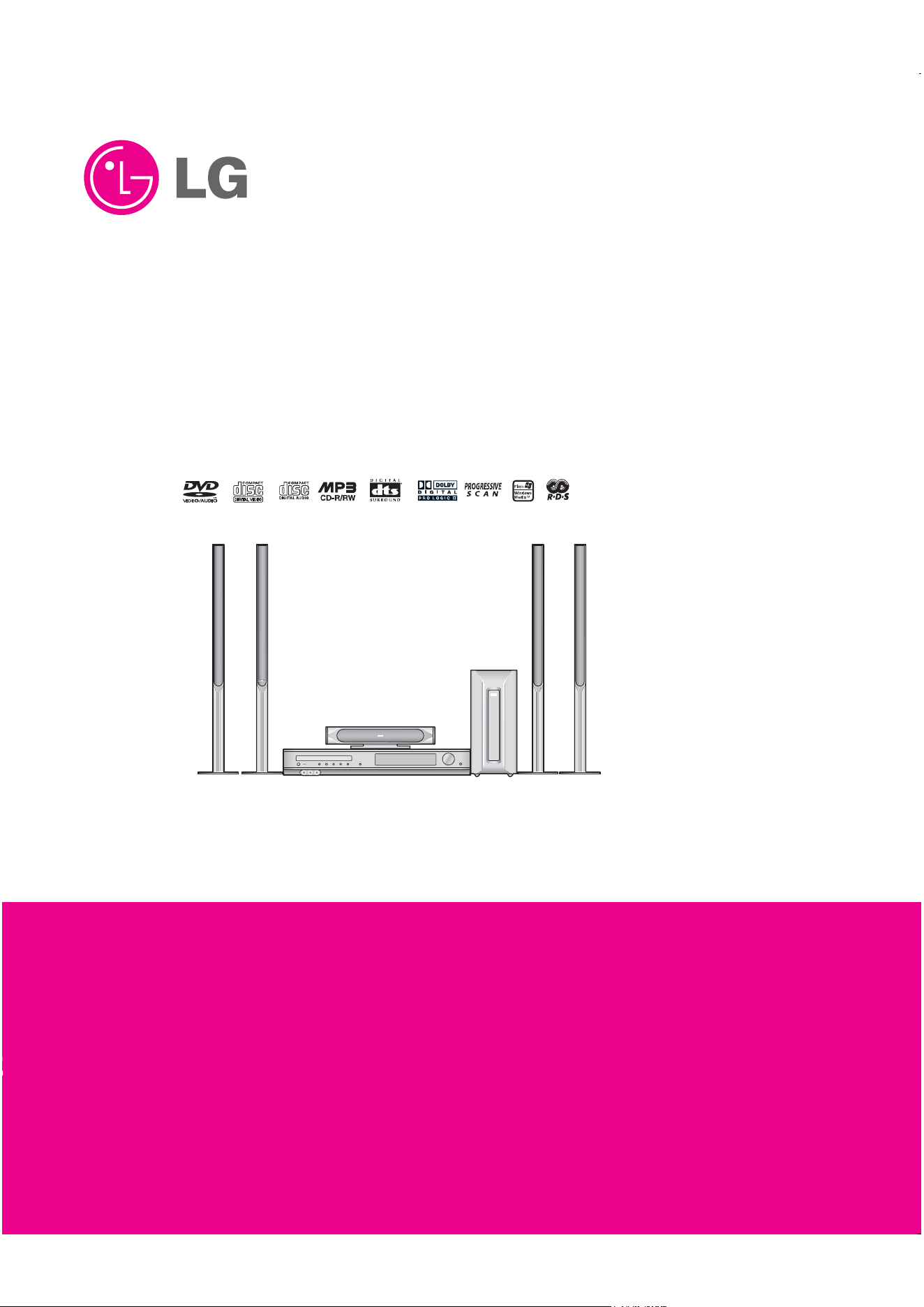
DVD/CD RECEIVER
SERVICE MANUAL
MODEL : LH-T6749(A)/
LHS-T6749C/LHS-T6749T/LHS-T6749W
http://biz.lgservice.com

- 1-1 -
[CONTENTS]
❍ SECTION 1.GENERAL
• SERVICING PRECAUTIONS . . . . . . . . . . . . . . . . . . . . . . . . . . . . . . . . . . . . . . . . . . . . . . . 1-2
• ESD PRECAUTIONS . . . . . . . . . . . . . . . . . . . . . . . . . . . . . . . . . . . . . . . . . . . . . . . . . . . . . 1-4
• SPECIFICATIONS . . . . . . . . . . . . . . . . . . . . . . . . . . . . . . . . . . . . . . . . . . . . . . . . . . . . . . . .1-5
❍ SECTION 2. AUDIO PART
• ELECTRICAL TROUBLESHOOTING GUIDE . . . . . . . . . . . . . . . . . . . . . . . . . . . . . . . . . . . . 2-1
• BLOCK DIAGRAM . . . . . . . . . . . . . . . . . . . . . . . . . . . . . . . . . . . . . . . . . . . . . . . . . . . . . . . . 2-5
• SCHEMATIC DIAGRAMS . . . . . . . . . . . . . . . . . . . . . . . . . . . . . . . . . . . . . . . . . . . . . . . . . . 2-7
• WIRNG DIAGRAMS . . . . . . . . . . . . . . . . . . . . . . . . . . . . . . . . . . . . . . . . . . . . . . . . . . . . . 2-21
• PRINTED CIRCUIT DIARGAMS . . . . . . . . . . . . . . . . . . . . . . . . . . . . . . . . . . . . . . . . . . . . 2-23
❍ SECTION 3.DVD PART
• DVD PART ELECTRICAL TROUBLESHOOTING GUIDE . . . . . . . . . . . . . . . . . . . . . . . . . . . .3-1
• DETAILS AND WAVEFORMS ON SYSTEM TEST AND DEBUGGING . . . . . . . . . . . . . . . . .3-8
• BLOCK DIAGRAM . . . . . . . . . . . . . . . . . . . . . . . . . . . . . . . . . . . . . . . . . . . . . . . . . . . . . . . 3-21
• DVD PART SCHEMATIC DIAGRAMS . . . . . . . . . . . . . . . . . . . . . . . . . . . . . . . . . . . . . . . . .3-25
❍ SECTION 4. EXPLODED VIEWS . . . . . . . . . . . . . . . . . . . . . . . . . . . . . . . . . . .4-1
❍ SECTION 5. SPEAKER PART . . . . . . . . . . . . . . . . . . . . . . . . . . . . . . . . . . . . .5-1
❍ SECTION 6. REPLACEMENT PARTS LIST . . . . . . . . . . . . . . . . . . . . . . . . . . .6-1
- 1-2 -
SECTION 1. GENERAL
❏ SERVICING PRECAUTIONS
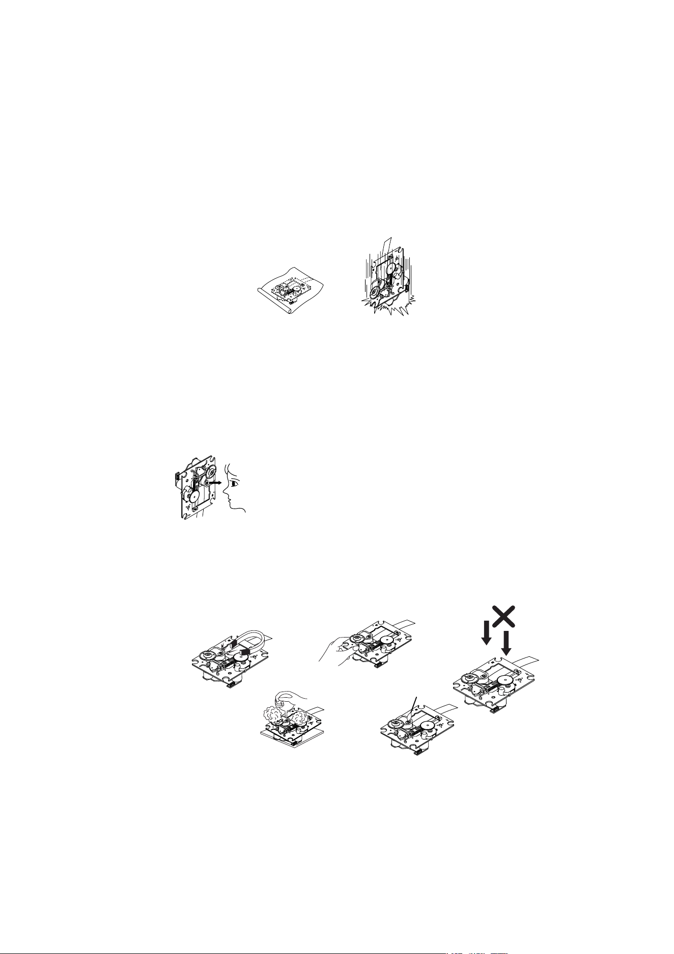
NOTES REGARDING HANDLING OF THE PICK-UP
1. Notes for transport and storage
1) The pick-up should always be left in its conductive bag until immediately prior to use.
2) The pick-up should never be subjected to external pressure or impact.
2. Repair notes
1) The pick-up incorporates a strong magnet, and so should never be brought close to magnetic materials.
2) The pick-up should always be handled correctly and carefully, taking care to avoid external pressure and
impact. If it is subjected to strong pressure or impact, the result may be an operational malfunction and/or
damage to the printed-circuit board.
3) Each and every pick-up is already individually adjusted to a high degree of precision, and for that reason
the adjustment point and installation screws should absolutely never be touched.
4) Laser beams may damage the eyes!
Absolutely never permit laser beams to enter the eyes!
Also NEVER switch ON the power to the laser output part (lens, etc.) of the pick-up if it is damaged.
5) Cleaning the lens surface
If there is dust on the lens surface, the dust should be cleaned away by using an air bush (such as used
for camera lens). The lens is held by a delicate spring. When cleaning the lens surface, therefore, a cotton
swab should be used, taking care not to distort this.
6) Never attempt to disassemble the pick-up.
Spring by excess pressure. If the lens is extremely dirty, apply isopropyl alcohol to the cotton swab.
(Do not use any other liquid cleaners, because they will damage the lens.) Take care not to use too much
of this alcohol on the swab, and do not allow the alcohol to get inside the pick-up.
Storage in conductive bag
Drop impact
NEVER look directly at the laser beam, and don’t let
contact fingers or other exposed skin.
Magnet
How to hold the pick-up
Conductive Sheet
Cotton swab
Pressure
Pressure
- 1-3 -
NOTES REGARDING COMPACT DISC PLAYER REPAIRS
1. Preparations
1) Compact disc players incorporate a great many ICs as well as the pick-up (laser diode). These components
are sensitive to, and easily affected by, static electricity. If such static electricity is high voltage, components
can be damaged, and for that reason components should be handled with care.
2) The pick-up is composed of many optical components and other high-precision components. Care must be
taken, therefore, to avoid repair or storage where the temperature of humidity is high, where strong magnet-
ism is present, or where there is excessive dust.
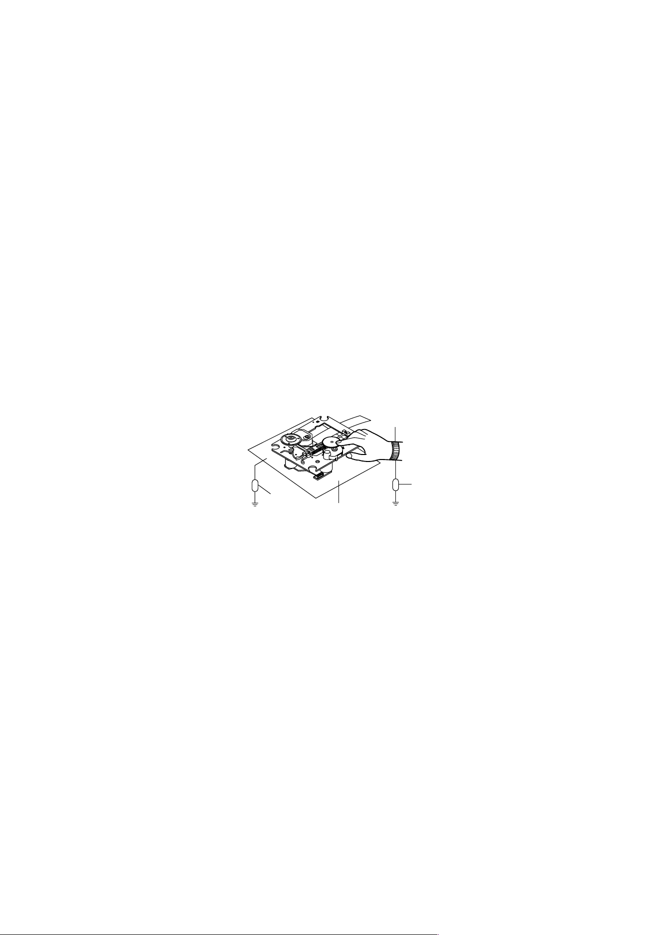
2. Notes for repair
1) Before replacing a component part, first disconnect the power supply lead wire from the unit
2) All equipment, measuring instruments and tools must be grounded.
3) The workbench should be covered with a conductive sheet and grounded.
When removing the laser pick-up from its conductive bag, do not place the pick-up on the bag. (This is
because there is the possibility of damage by static electricity.)
4) To prevent AC leakage, the metal part of the soldering iron should be grounded.
5) Workers should be grounded by an armband (1M Ω)
6) Care should be taken not to permit the laser pick-up to come in contact with clothing, in order to prevent sta-
tic electricity changes in the clothing to escape from the armband.
7) The laser beam from the pick-up should NEVER be directly facing the eyes or bare skin.
Resistor
(1 Mohm)
Conductive
Sheet
Resistor
(1 Mohm)
Armband
- 1-4 -
❏ ESD PRECAUTIONS
Electrostatically Sensitive Devices (ESD)
Some semiconductor (solid state) devices can be damaged easily by static electricity. Such components
commonly are called Electrostatically Sensitive Devices (ESD). Examples of typical ESD devices are integrated
circuits and some field-effect transistors and semiconductor chip components. The following techniques should
be used to help reduce the incidence of component damage caused by static electricity.
1. Immediately before handling any semiconductor component or semiconductor-equipped assembly, drain off
any electrostatic charge on your body by touching a known earth ground. Alternatively, obtain and wear a
commercially available discharging wrist strap device, which should be removed for potential shock reasons
prior to applying power to the unit under test.
2. After removing an electrical assembly equipped with ESD devices, place the assembly on a conductive sur-
face such as aluminum foil, to prevent electrostatic charge buildup or exposure of the assembly.
3. Use only a grounded-tip soldering iron to solder or unsolder ESD devices.
4. Use only an anti-static solder removal device. Some solder removal devices not classified as "anti-static" can
generate electrical charges sufficient to damage ESD devices.
5. Do not use freon-propelled chemicals. These can generate electrical charges sufficient to damage ESD
devices.
6. Do not remove a replacement ESD device from its protective package until immediately before you are
ready to install it. (Most replacement ESD devices are packaged with leads electrically shorted together by
conductive foam, aluminum foil or comparable conductive materials).
7. Immediately before removing the protective material from the leads of a replacement ESD device, touch the
protective material to the chassis or circuit assembly into which the device will by installed.
CAUTION : BE SURE NO POWER IS APPLIED TO THE CHASSIS OR CIRCUIT, AND OBSERVE ALL
OTHER SAFETY PRECAUTIONS.
8. Minimize bodily motions when handing unpackaged replacement ESD devices. (Otherwise harmless motion
such as the brushing together of your clothes fabric or the lifting of your foot from a carpeted floor can gen-
erate static electricity sufficient to damage an ESD device).
CAUTION. GRAPHIC SYMBOLS
THE LIGHTNING FLASH WITH APROWHEAD SYMBOL. WITHIN AN EQUILATERAL TRIANGLE, IS
INTENDED TO ALERT THE SERVICE PERSONNEL TO THE PRESENCE OF UNINSULATED “DAN-
GEROUS VOLTAGE” THAT MAY BE OF SUFFICIENT MAGNITUDE TO CONSTITUTE A RISK OF
ELECTRIC SHOCK.
THE EXCLAMATION POINT WITHIN AN EQUILATERAL TRIANGLE IS INTENDED TO ALERT THE
SERVICE PERSONNEL TO THE PRESENCE OF IMPORTANT SAFETY INFORMATION IN SERVICE
LITERATURE.
- 1-5 -
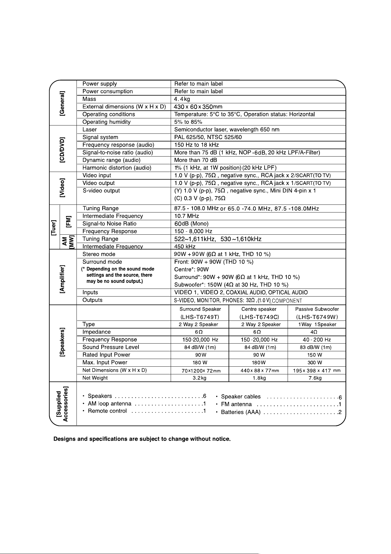
❏ SPECIFICATIONS

- 1-6 -
- 2-1 -
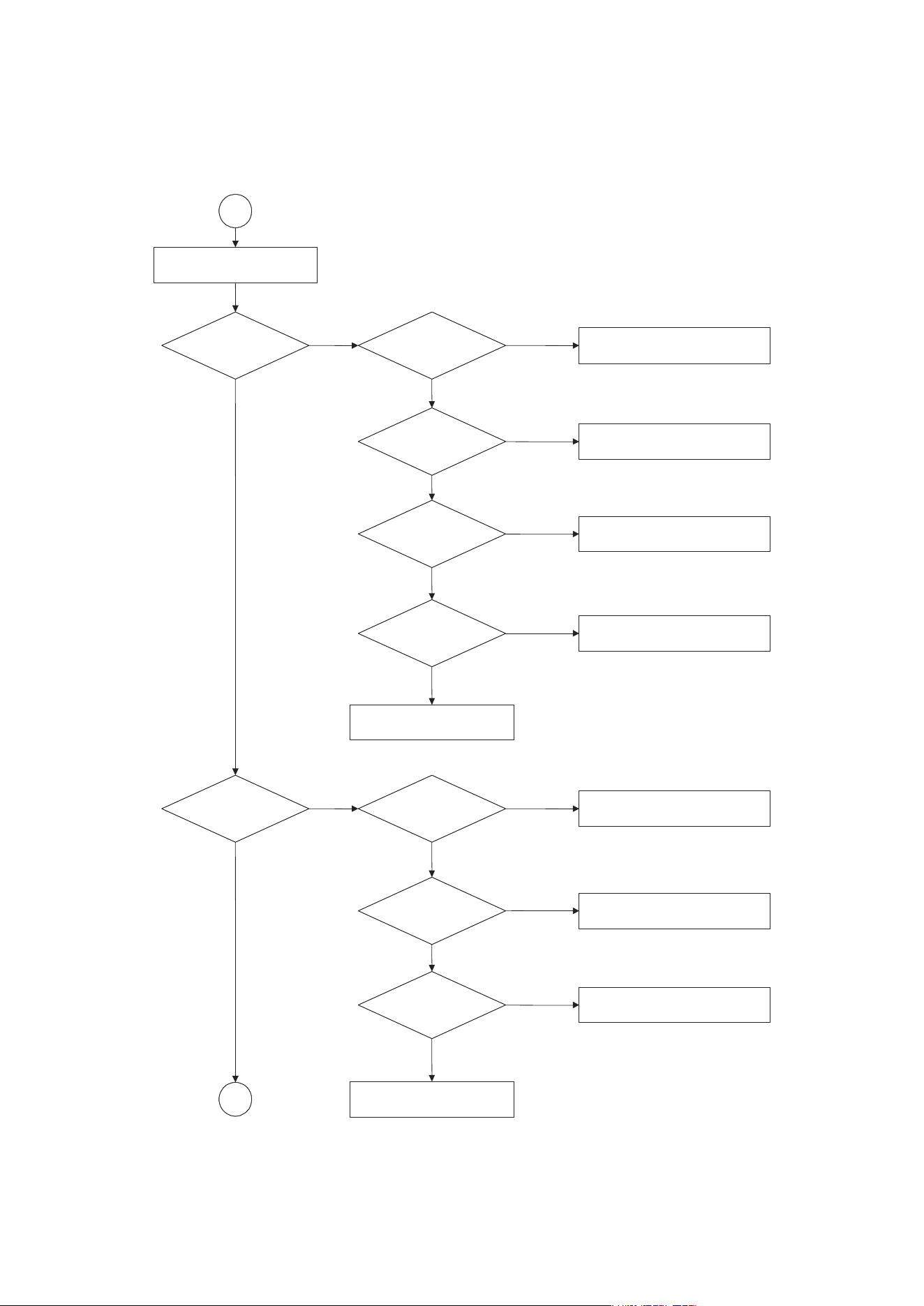
❏
ELECTRICAL TROUBLESHOOTING GUIDE
INSERT
POWER CORD.
TURN ON
THE RED LED?
IS POWER ON?
CHECK POWER PLUG
AND POWER SUPPLY CIRCUIT.
DOES INITIAL
READ WORK?
DOES IT PLAY?
YES
NO
YES
YES
OK
NO
YES
NO
NO
CHECK POWER SUPPLY CIRCUIT.
CHECK LASER CIRCUIT.
CHECK TRACKING SERVO CIRCUIT.
TURN POWER ON.
CHECK FOCUS CIRCUIT.
CHECK DISC.
DOES IT OUTPUT
AUDIO?
YES
NO
CHECK AUDIO CIRCUIT.
1. Power check flow
SECTION 2. AUDIO PART
- 2-2 -
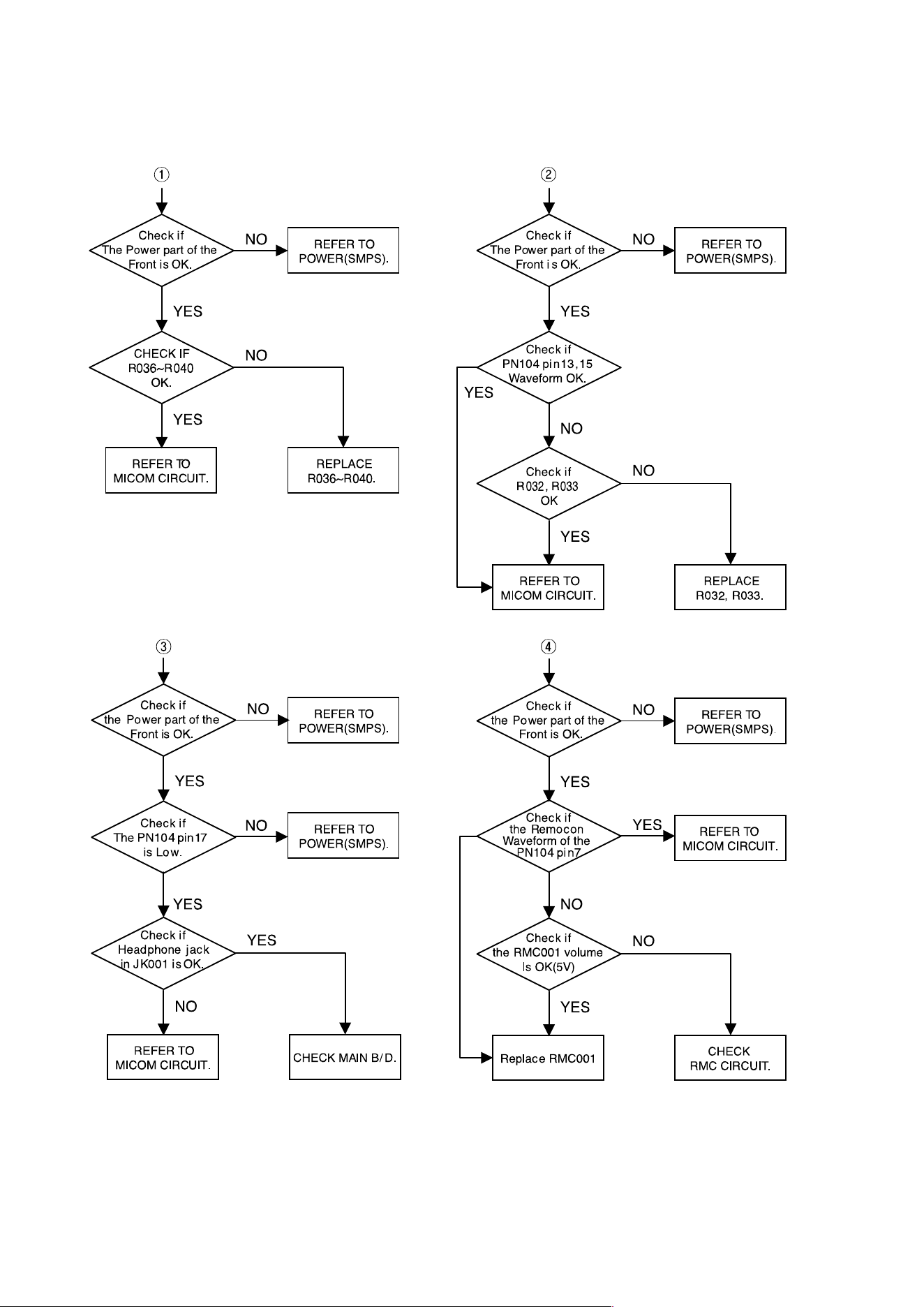
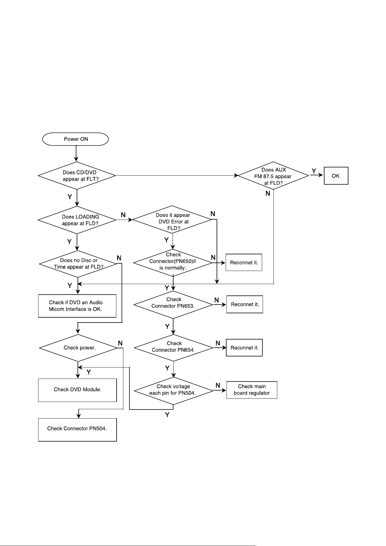
2.AUDIO µ.COM CIRCUIT
POWER ON
Does it appear
DVD Error at
FLD?
Does AV 1/2, TV, AUDIO,
OPTICAL IN, COAXIAL IN, FM87.5
appear at FLD?
Check
Connector(PN902)if
is normally.
Check power part
of Main B/D.
Check oscillator
of x101.
Check if IC101
PIN1 is High.
Check if IC101
PIN11 is High.
Check if IC101 PIN
17, 46, 72, 90 is high
(5V).
Check if IC101
PIN26 is High.
Replace IC101.
Does CD/DVD
appear at FLD?
Reconnet it.
Refer to SMPS
OK.
Refer to oscillator
Circuit.
Check DVD Reset Waveform.
Check IC101 Reset Wavefrom.
Check 5V line.
Check Power dection Circuit.
Does LOADING
appear at FLD?
Does no Disc or
Time appear at FLD?
Check if DVD an Audio
Micom Interface is OK.
Check power.
Check DVD Module.
Check SMPS.
- 2-3 -
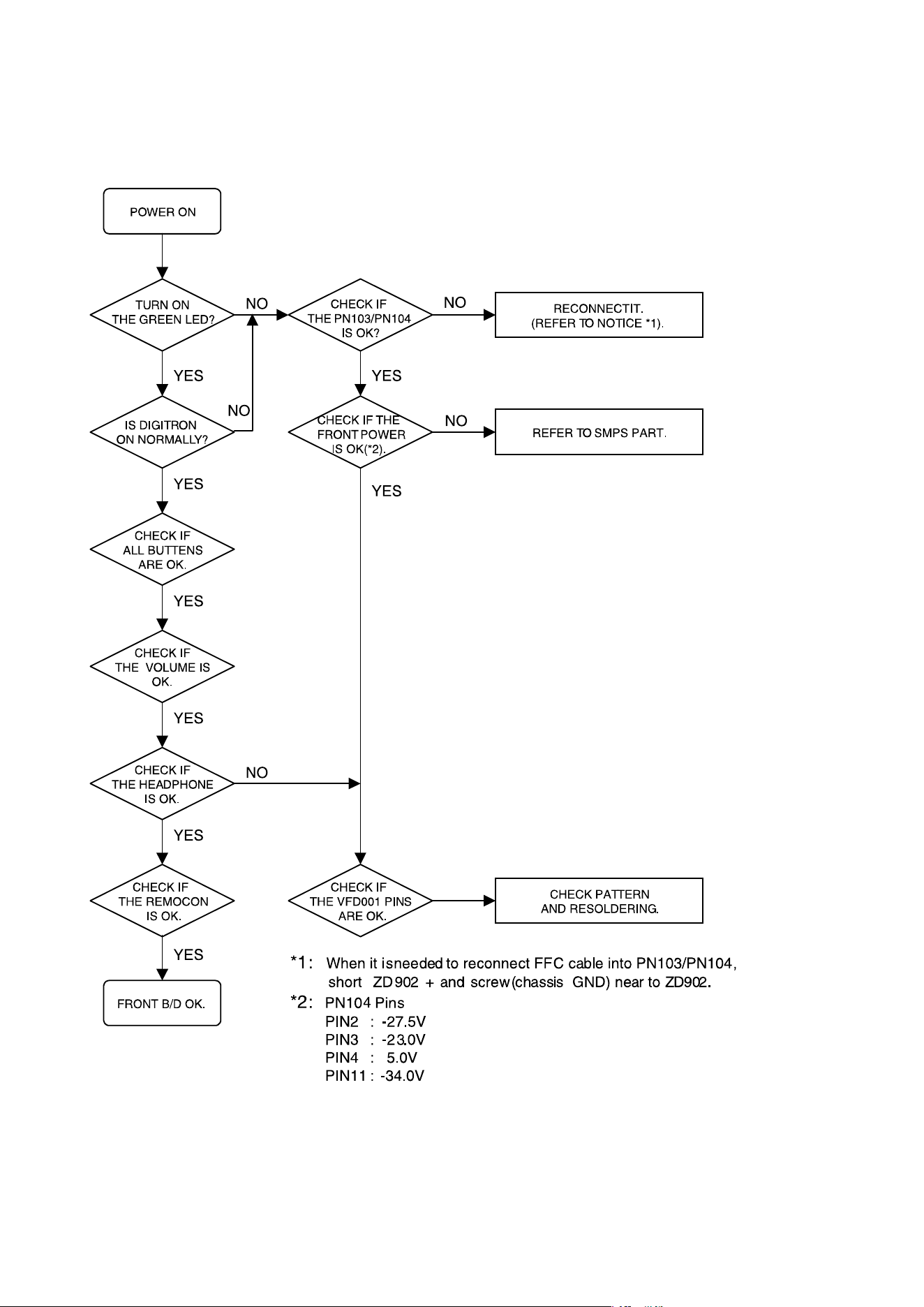
3.FRONT CIRCUIT (1/2)
- 2-4 -
4.FRONT CIRCUIT (2/2)
- 3-1 -
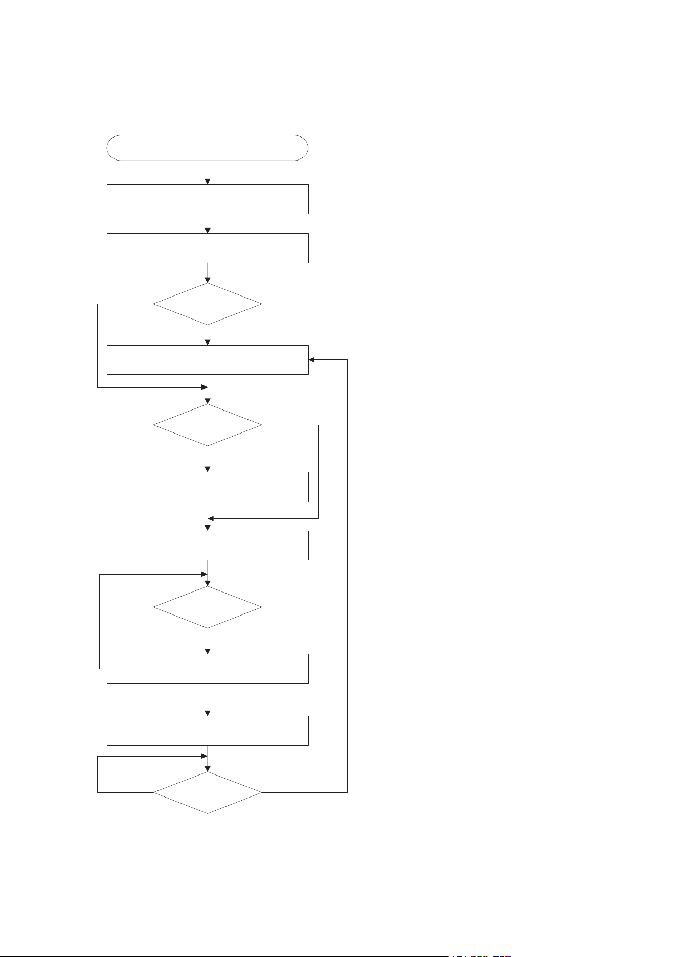
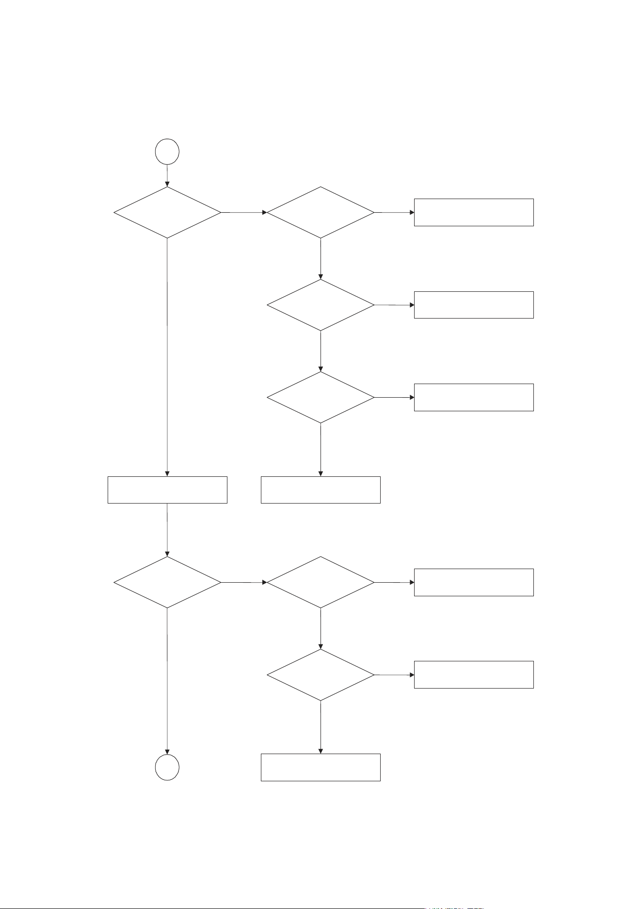
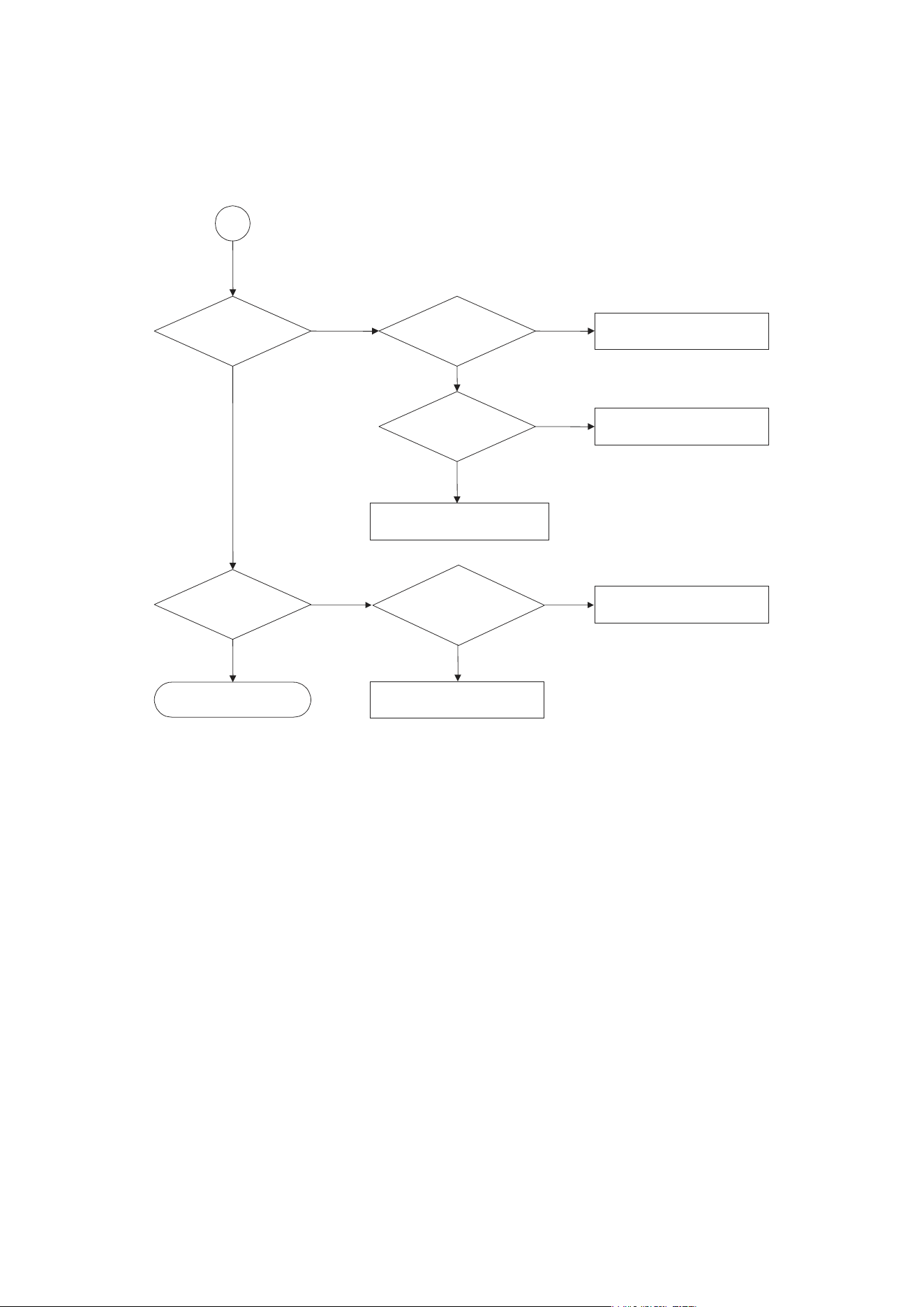
1. Power check flow
❏
ELECTRICAL TROUBLESHOOTING GUIDE
SECTION 3. DVD PART
- 3-2 -
2. System operation flow
Power On
1. 8032 initializes SERVO, DSP & RISC registers
2. Write RISC code to SDRAM
3. Reset RISC
Show LOGO
Tray Closed?
Tray Close to Closed position
NO
SLED at Inner
Side ?
SLED Moves to Inner Positi on
NO
YES
YES
Reci eve
OPEN/CLOSE
Key?
1. Execute Pressed Key & IR Key
2. System operation Routine Loop
NO
1. Stop Playback & Open Tray
2. Display tray open message & LOGO
Receive
CLOSE Key?
NO
YES
YES
1. Judge whether have disc and disc type
2. Jump to related disc reading procedure
- 3-3 -
3. Test & debug flow
TEST
Check the AC Voltage
Power PCBA(110V or 220V)
NO
Replace power PCBA or
AC transformer.
YES
Switch on the Power PCBA
Is the DC Voltage
outputs OK?
(5V,1.8V,3.3V,8V,12V)
Repair or Replace Power PCBA
NO
Make sure the main PCBA don't
short on VCCs and switch it on.
YES
Is 3.3V and 1.8V DC
outputs normal on main
PCBA?
Check the regulators or related diodes.
NO
YES
Connect to PC RS232 Cable and
update the FLASH memory code.
Update FLASH
successfully?
A
YES
NO
1. Check 27MHz system clock.
2. Check system reset circuit.
3. Check FLASH R/W enable signal PRD,RWR.
4. Check RS232 SIGNALS.
5. Check FLASH Memory related circuit.
- 3-4 -
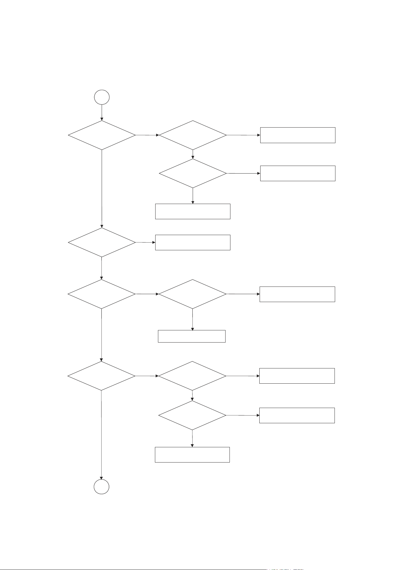
A
RESET or Power On.
NO NO
YES
NO
YES
NO
YES
YES
B
NO
NO
NO
YES
YES
NO
NO
YESYES
YES
Show LOGO?
Flash Memory operates
properly?
Check connection lines between FLASH
& MT1389 and the FLASH access time
whether is suitable or not.
SDRAM works properly?
Check connection lines between
SDRAM & MT1389 and the SDRAM
is damaged.
MT1389 VIDEO outputs
properly?
Check the related circuit of MT1389.
Have TV signal output?
Check the filtering and amp circuit of
TV signal.
Check AV cable connection
to TV set.
Does Tray move
inside when it is not
at closed position?
Normal TROUT &
TRIN signals?
Check the load OPEN & CLOSE
switch
Normal TRCLOSE &
TROPEN signal?
Normal LOAD+ &
LOADsignal?
Check the cable connection
between main PCBA and loader.
Check the Tray control IO pins on
MT1389 & IP4504.
Check the Tray control amplifying
circuit on Motor driver.
- 3-5 -
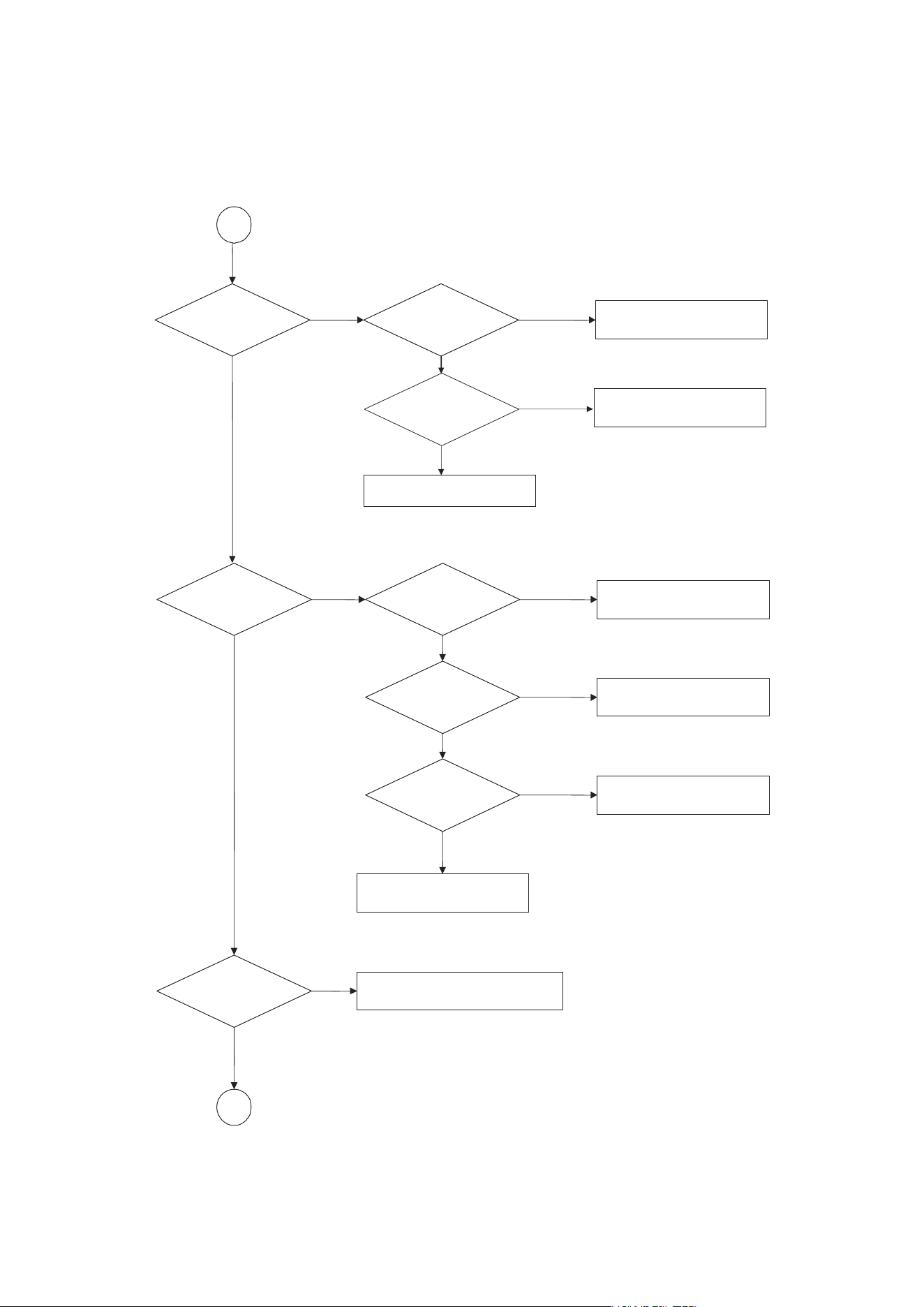
B
NO NO
NO
NO
NO NO
NO
YES YES
YES
YES
YESYES
YES
Does
the SLED move
to inner side when it is at
outter position?
Motor Driver STBY
Pin is High?
Check the connection line of
STBY signal.
Is FMSO DC Level higher
than 1.4V?
Check the related circuit of
FMSO.
SL+ and SL- output
properly?
Check the amp circuit on motor
driver.
Check the cable connection with
MECHA.
Do not put in disc and tray
close.
C
Optical Lens has
movements for searching
Focus?
Proper FOSO outputs
to motor driver?
Check FOSO connection on
MT1389 and motor dirver.
Proper F+ & F- outputs?
Check the amp circuit on motor
dirver.
Check cable connect on with
pick-up head.
- 3-6 -
D
C
YES
NO
YES
YES
NO
NO
Does spindle rotate?
Proper DMSO signal on
MT1389
Check DMSO related
circuit on MT1389.
SP+ & SP- output
properly?
Check the spindle control
amp circuit of motor
driver.
Check the cable connection
between spindle and main PCBA.
YES
YES
NO
NO
Laser turns on when
reading disc?
NO
NO
YES
NO
YES
YES
NO
LD01 or LD02 output
properly?
Check the laser power circuit
on MT1336 and connecting to
power transistor.
Collector voltage of
power transistor is OK?
Check the related circuit on
laser power transistor
Check cable connection between
transistor ouput and pick-up
head.
Put disc in? Laser off
Disc ID is correct?
Proper RFL signal
on MT1389?
Check the related circuit
on MT1389 RFL signal.
Check LDO1 & LDO2 signal
YES
- 3-7 -
YES
NO
YES
YES
D
NO
NO
NO
YES
NO
E
YES
Normal TEO Signal on
MT1389?
Check the related
circuit on MT1389
Track On OK?
Properly TRSO signal
on MT1389?
T+ & T- output
properly?
Check the TRSO
connection on MT1389
and motor dirver.
Check the tracking control
amp circuit on motor
driver.
Check cable connection on
pick-up head.
Disc is play ?
Check RFO & RFLVL signal waveform.
NO NO
YES
YES
YES
Focus ON OK?
Proper signals on
A,B,C,D of MT1389
Check connections between
MT1389 and pick-up head.
Check FEO signal
on MT1389
Check FOSO signal on MT1389
Check the FOSO connection on
MT1389 and motor driver.
YES
NO
- 3-8 -
Normal IR.VFD & Front
pannel key functions?
Communications between
IR.VFD Front pannelkey & MT1389
is normally?
Check communication lines on
MT1389.
NO
YES
Check the cable connection on
Front pannel.
TEST END
YES
Normal Audio output
when disc playback?
Audio PWM IC received
correct data stream?
Check connection between MT1379
& Audio PWM IC.
Normal Audio PWM IC
out?
Check the related
circuit of Audio PWM IC.
Check Audio filter,amplify,mute
circuit.
NO NO
NO
YES
YES
YES
E
NO
- 3-9 -
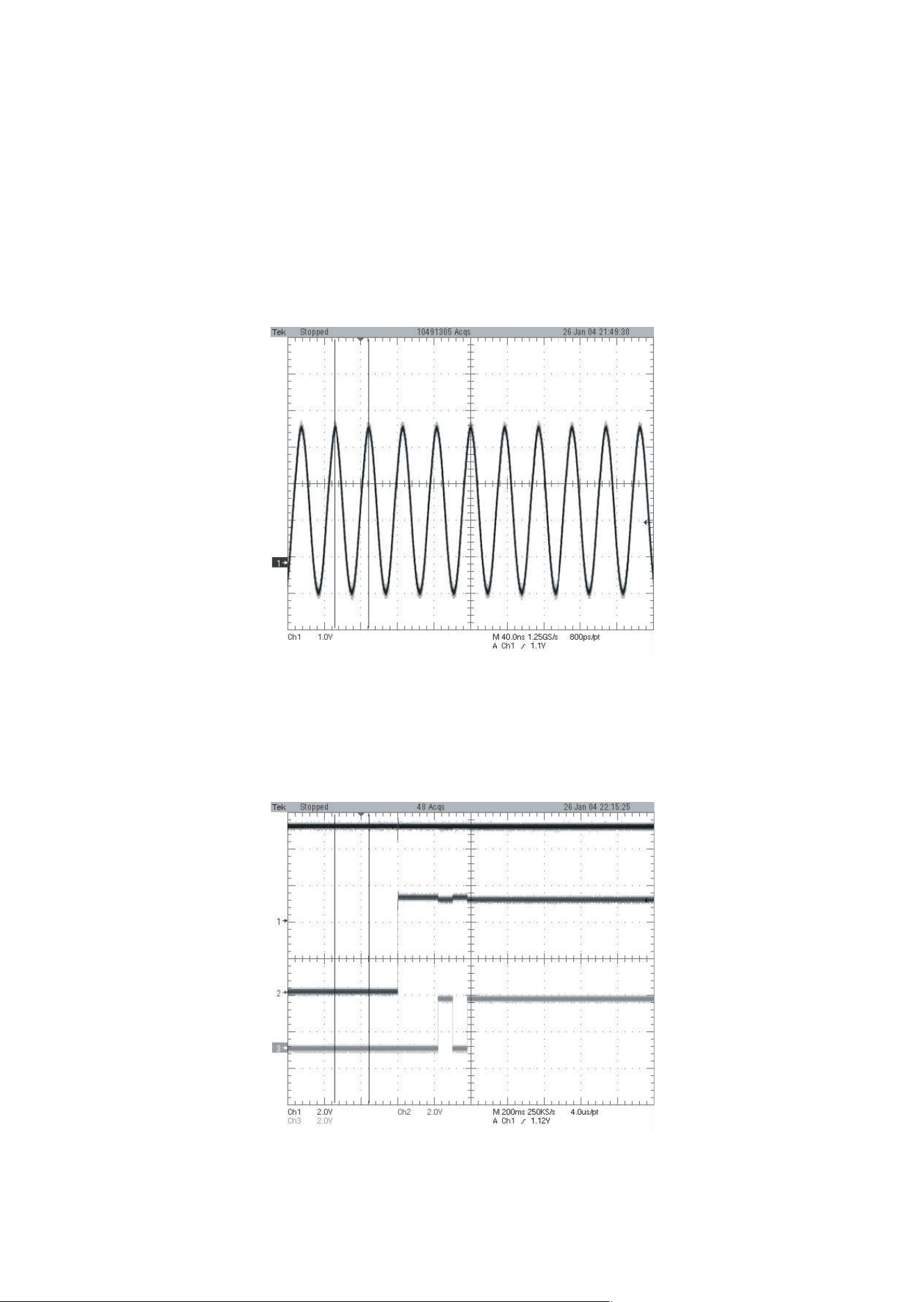
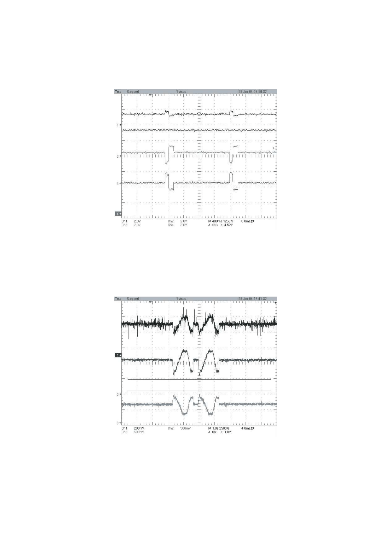
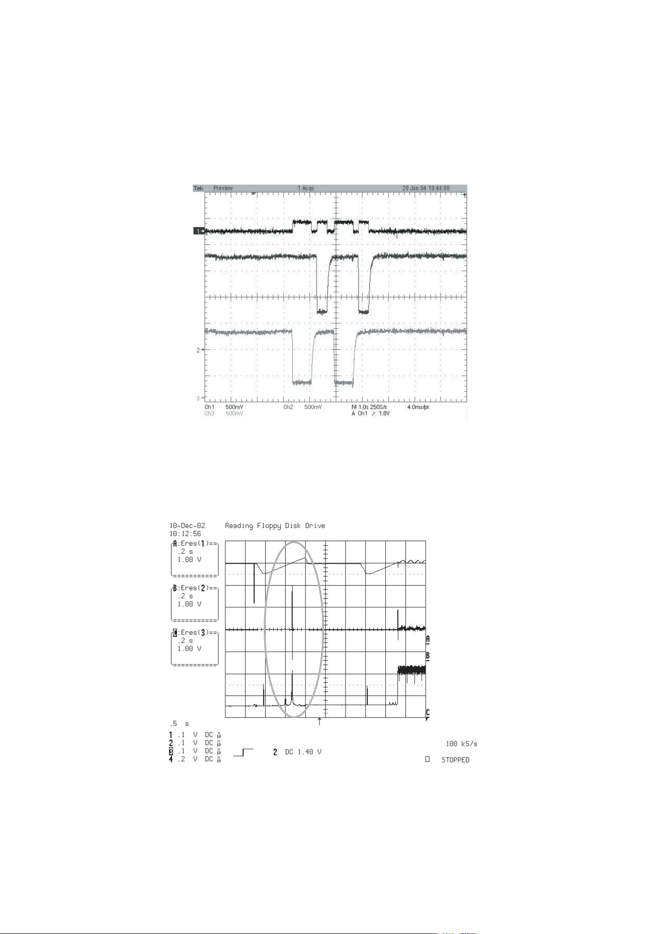
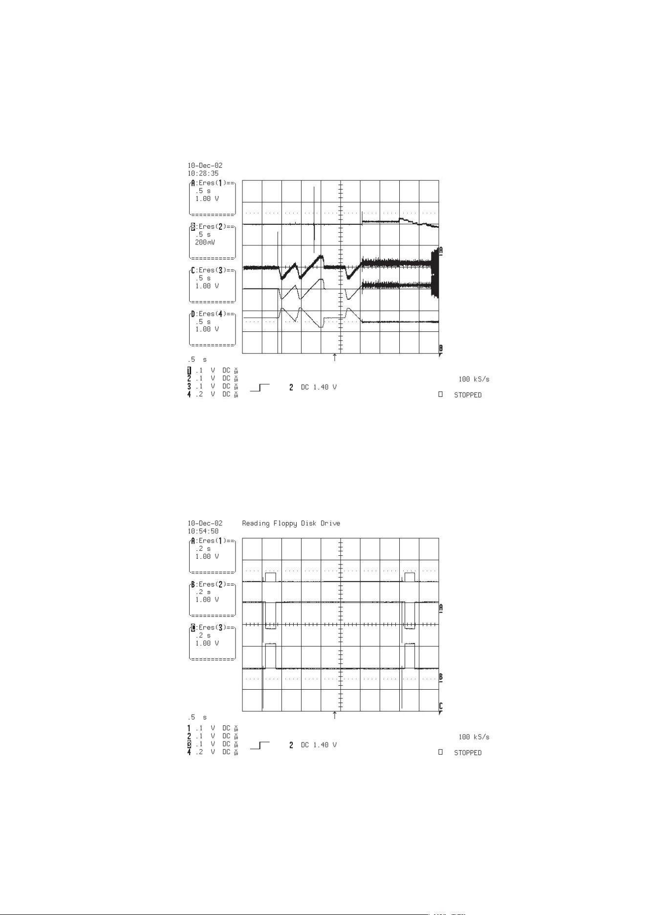
FIG 1-1
FIG 1-2
❏ DETAILS AND WAVEFORMS ON SYSTEM TEST
AND DEBUGGING
1. SYSTEM 27MHz CLOCK,RESET,FLASH R/W SIGNAL
1) MT1379 main clock is at 27MHz(X501)
2) MT1336 reset is high active
- 3-10 -
FIG 1-3
FIG 1-4
3) RS232 waveform during procedure(Downloading)
4) Flash R/W enable signal during download(Downloading)
- 3-11 -
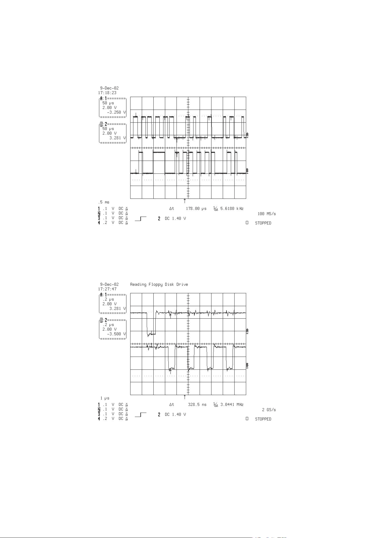
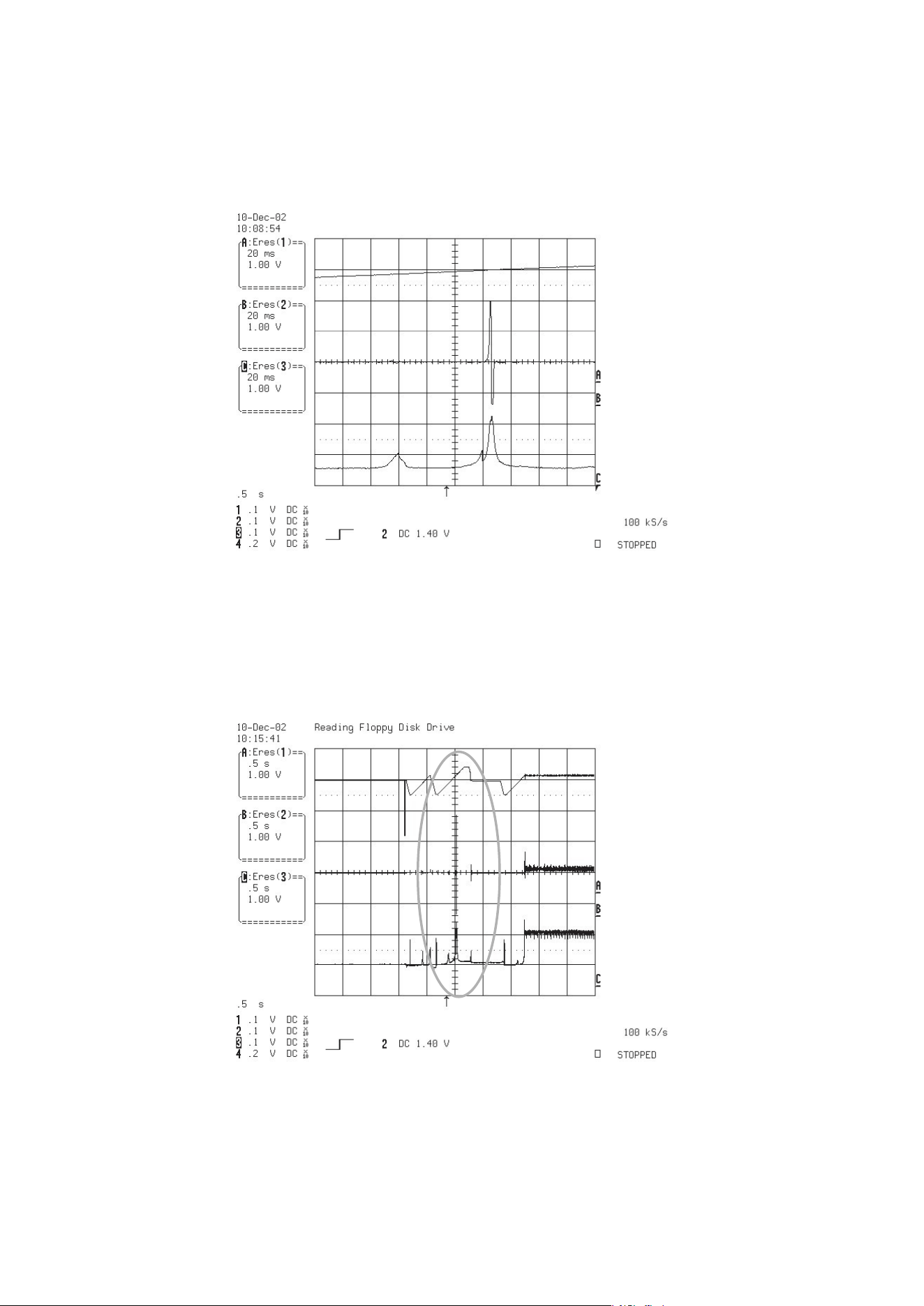
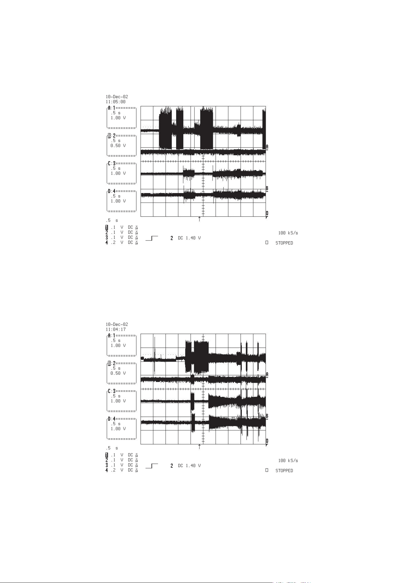
FIG 2-1
FIG 3-1
2. SDRAM CLOCK
1) MT1379 main clock is at 27MHz(X501)
3. TRAY OPEN/CLOSE SIGNAL
- 3-12 -
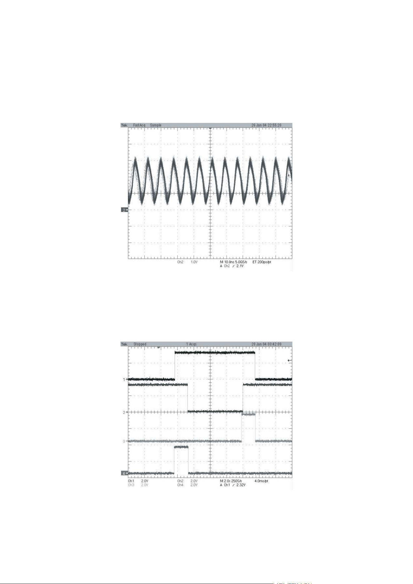
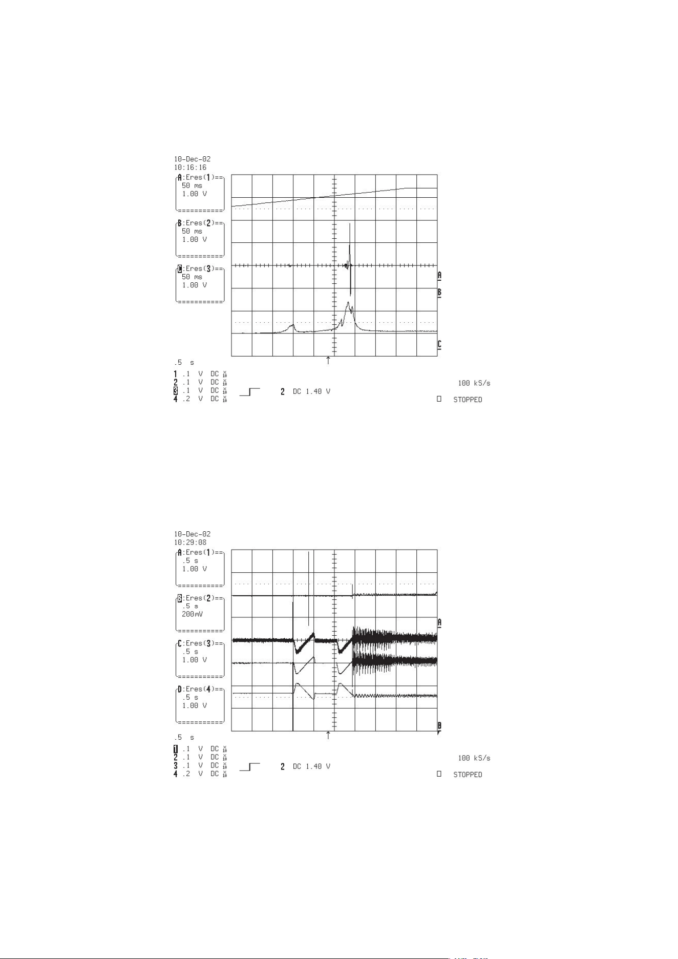
FIG 4-1
FIG 5-1
4. SLED CONTROL RELATED SIGNAL (NO DISC CONDITION)
5. LENS CONTROL RELATED SIGNAL(NO DISC CONDITION)
- 3-13 -
FIG 6-1
FIG 7-1
6. LASER POWER CONTROL RELATED SIGNAL
(NO DISC CONDITION)
7. DISC TYPE JUDGEMENT W VEFORM
- 3-14 -
FIG 7-2 (DVD)
FIG 7-3 (CD)
- 3-15 -
FIG 7-4 (CD)
FIG 8-1 (DVD)
8. FOCUS ON W VEFORM
- 3-16 -
FIG 8-2 (CD)
FIG 9-1
9. SPINDLE CONTROL W VEFORM (NO DISC CONDITION)
- 3-17 -
10. TRACKING CONTROL RELATED SIGNAL(System checking)
FIG 10-1 (DVD)
FIG 10-2 (CD)
- 3-18 -
FIG 11-1 (DVD)
FIG 12-1
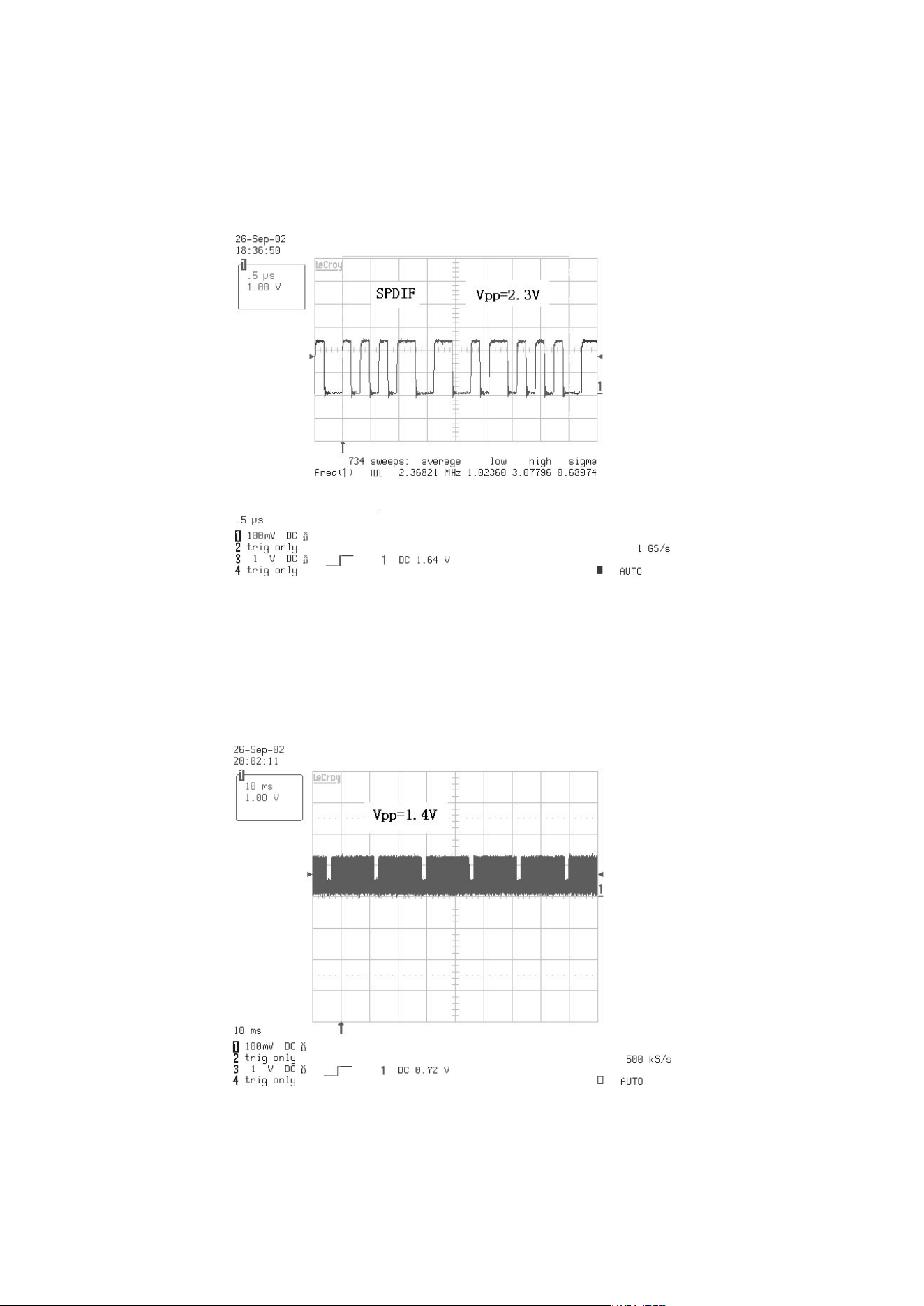
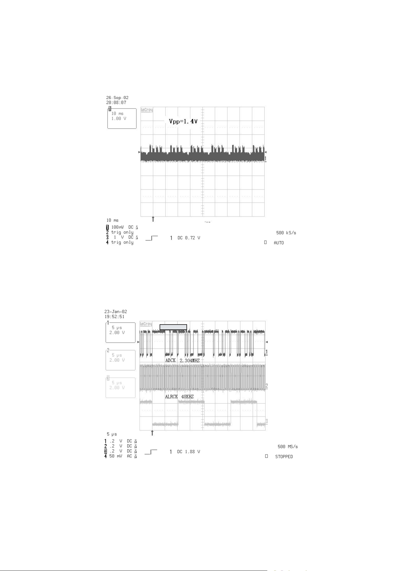
11. MT1389 AUDIO OPTICAL AND COAXIAL INPUT (SPDIF)
12. MT1389 VIDEO OUTPUT WAVEFORM
1)100%
- 3-19 -
ADAT0~3
FIG 12-2
FIG 13-1
2) COMPOSITE VIDEO SIGNAL
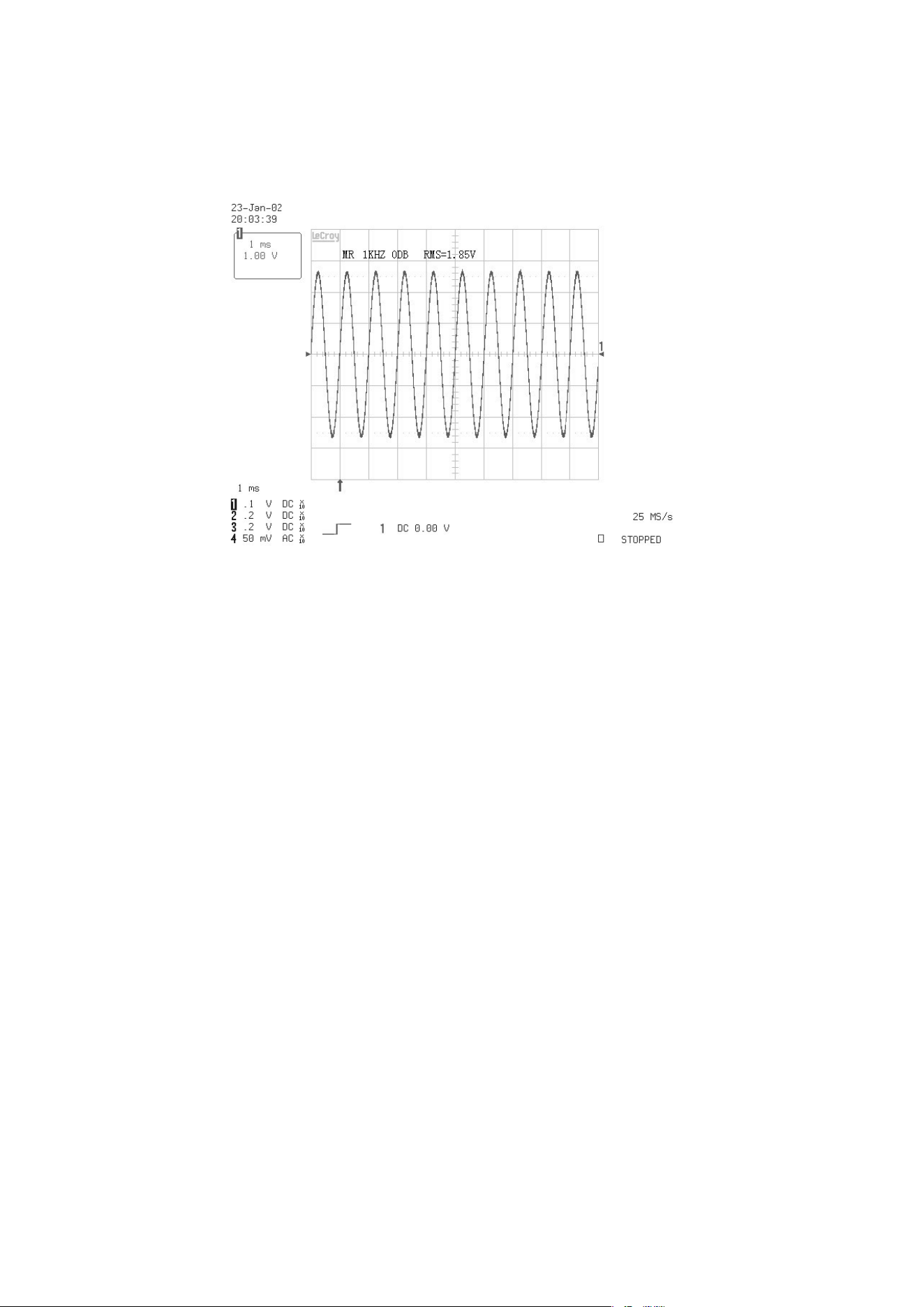
13. MT1389 AUDIO OUTPUT TO PWM IC
- 3-20 -
FIG 14-1
14. AUDIO OUTPUT FROM PWM IC
- 3-21 -
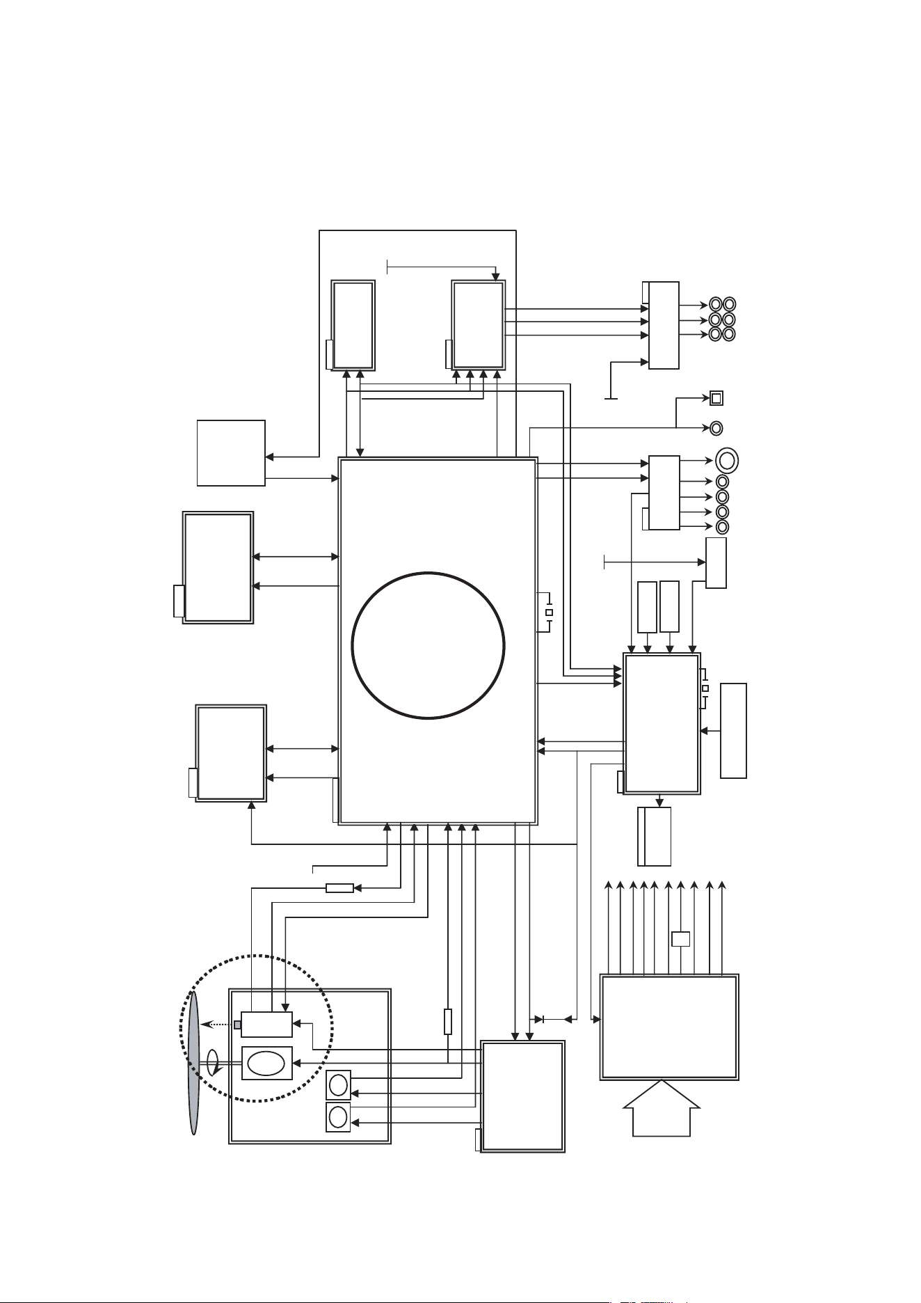
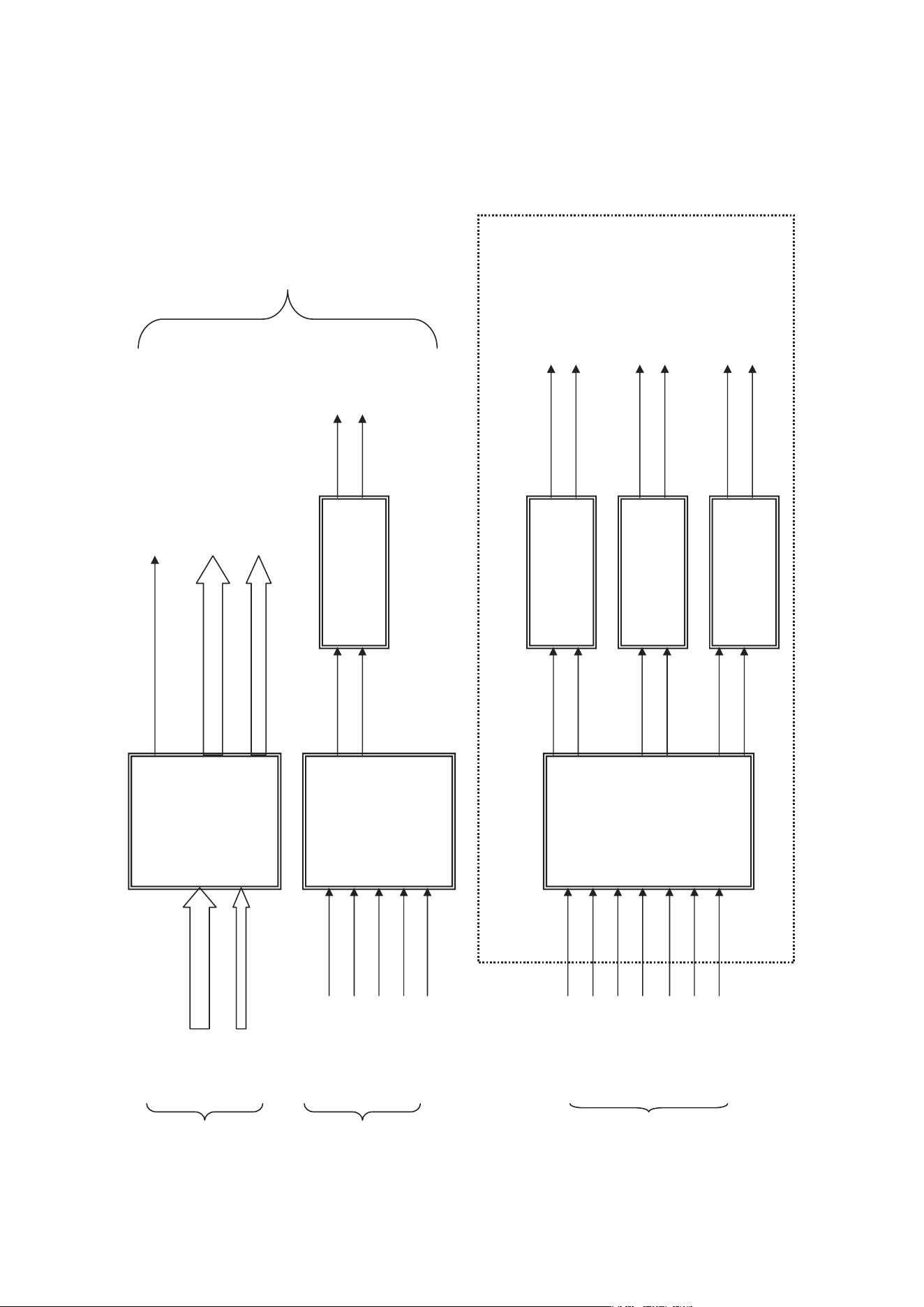
❏ BLOCK DIAGRAM
1. Overall Block Diagram
M
M
DISC
SPINDLE
MOTOR
LOADING
MOTOR
DECK MECHANISM
DVD : A,B,C,D,RF0
CD : A,B,C,D,E,F,RF0
CDMDI,DVDMDI
PICK
UP
KEY Input
6MHz
B/Pb
IC602
MX29LV160T
2/4M
16/32BIT
FLASH ROM
M-RESET
ROMAD[0:
19]
ROMRD
ROMWR
MD[00:15]
FL
FR
CVBS
R/Pr G/Y
RL
RR
CENTER
WOOFER
TV_DAC[0:3]
Y
C
FL
FR
RL
RR
CENTER
WOOFER
VF+
AC 90V~240V
50HZ/60Hz
VF-
-27VA
5V
VD33,VD33D
12V
27MHz
PWRCTL
3.3V-M1
IC606
KS24C02
EEPROM
IC701~4
DIGITAL
POWER IC
RC901
R/C
IC903
RESET IC
LOAD[+,-]
FOCUS[+,-]
TRACK[+,-]
SPINDLE[+,-]
SLED
(FEEDING)
MOTOR
SLED[+,-]
M
VD33D
VD33D
VD18/VD33
3V3M
IC605
MM1623XFBE
VIDEO BUFFER
RS232_TXD
IECDAOUT
COAXIAL
SPDIF
D2_T[1:3]
SCART_16:9
RGB_SEL
3V3M
CDLD,DVDLD,SVREF21
5V/8V
HOMESW
INSW,OUTSW
ROMDATA[0:7]
5.2VA
IC101
AUDIO MICOM
M_REQ
POWER
BOARD
VFD_RXD
S_REQ
5.2VA
8V
DMUTE
IIC/VFD/DAC_SCK
IC603
4M
16BIT
4Bank
SDRAM
VD33D
MA[00:11]
DMCLK
CSJ
BA0
BA1
DQM
WEJ
CASJ
RASJ
IIC/VFD/DAC_TXD
IC601
MTK MT1389
+12V
+12V5V
YC_MIX
VIDEO_SW
SER[0:2],DAC_ML1
OPEN,CLOSE,SLEGP,SPINDLE,FOCUS,TRACK,SVREF
DAC_RST
CD_DVD, VR_CD,VR_DVD
CD_DVD_CT
XSFGN,XSFGP
CN601
RS232
Download
RS232_RXD
3.3V
3.3V-M
U7
VD18
IC301
PS9818
(PWM IC)
IC201
IP4504
Motor Drive
DRVSB
OPU_SEL
JACK
TRIGGER
-27VA/VF+/VF-
DIG901
FLD DISPLAY
Pick-up
RF+
MPEG IC
- 3-22 -
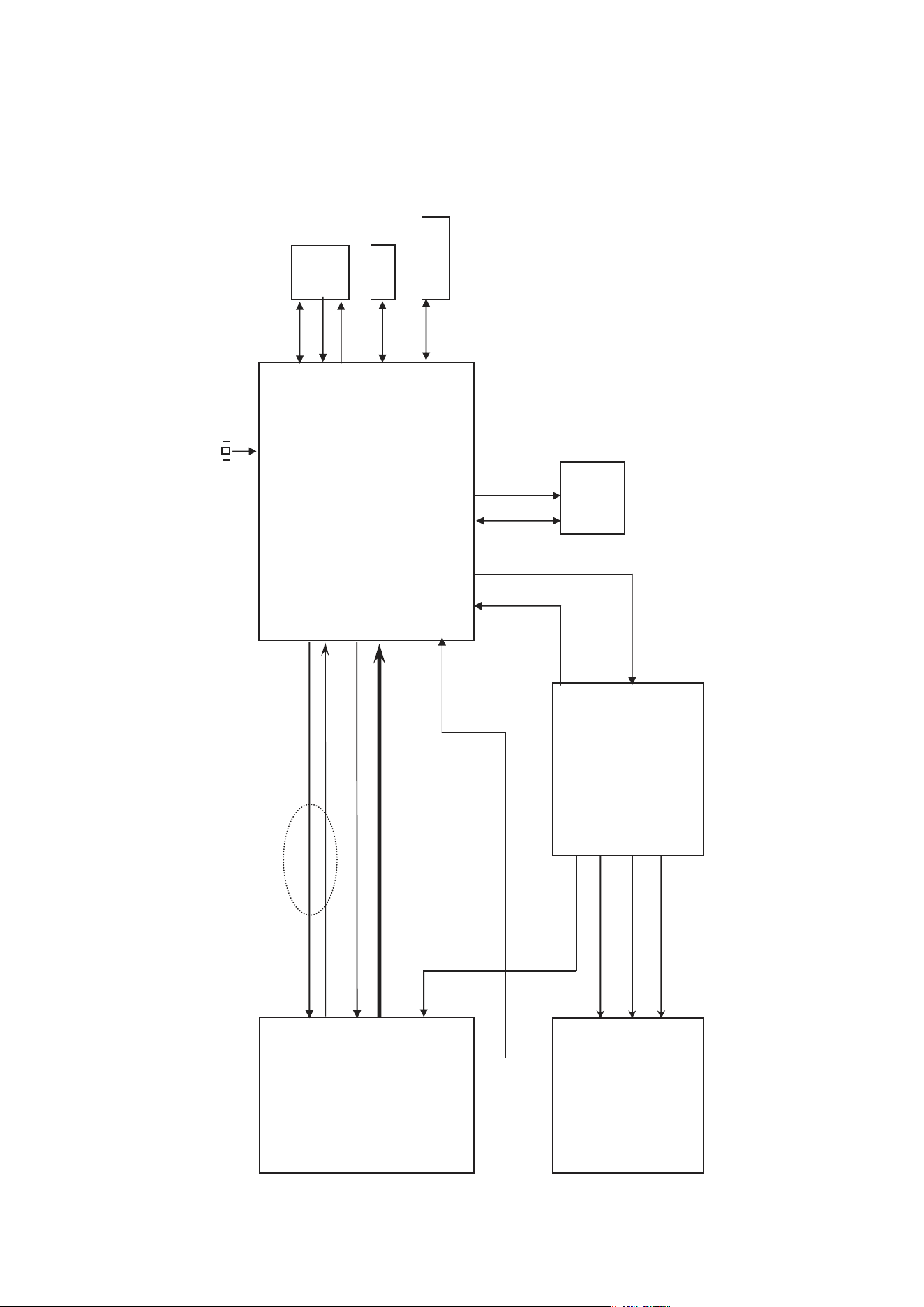
2. SERVO Block Diagram
IC201
IP4504
Motor Driver
DVD: A,B,C,D, RFO
CD: A,B,C,D, E, F,RFO
SP+, SP-
M/D
PICK
UP
FOSO,TRSO,FMSO
DMSO,,TROPEN
ADIN
F+, F-, T+, T-
SL+, SL-
LOAD+, LOAD-
LD0 1, LDO 2, IOA
MDI 1
ALPC
V20, PICKSEL
LIMIT,TRIN,TROUT
TRCLOSE
STBY,V1P4
IC603
4M x 16bit
SDRAM
MA[0:11]
DQM0 ,DQM1
WE#,CAS#,RAS#
CS#,BA0,BA1
SDCLK
SDCKE
DQ[0:15]
FLASH
ROM
PRD#, PWR#
PCE#
AD[0:7]
A[0:20]
EEP
ROM
SCL, SDA
RS232C(MTK)
RXD, TXD
X501
27MHz
X-TAL
IC601
MT1389
DVDPLAYER
ONE CHIP
- 3-23 -
3. MPEG & MEMORY Block Diagram
IC606
EEPROM
IC601 (MPEG + DSP + RF)
MT1389
IC602
FLASH MEMORY
(16 M )
VIDEO
Interface
AUDIO
Interface
AUDIO MICOM
IC603
SDRAM
64M
DCLK,WE,CAS,RAS
CS,DCKE,MA[0:10]
DQM0,DQM1
DQ[0:15]
X501
27MHz
SCL,SDA
Y2(Y),Y3(Color)
Y4(Y),Y5(Cb),Y6(Cr)
ASPECT(16:9)
ACLK,ALRCK,ABCK
MUTE,VSCK,VSDA
ASDTA[0:3]
ASTB,SCL,SDA
ASPDIF
PWR,PCE,PRD
A[0:20]
AD[0:7]
VFD_SCK
VFD_TXD
M_REQ
SCKO,TXDO,M-REQ
URST,S_REQ
VFD_RXD
- 3-24 -
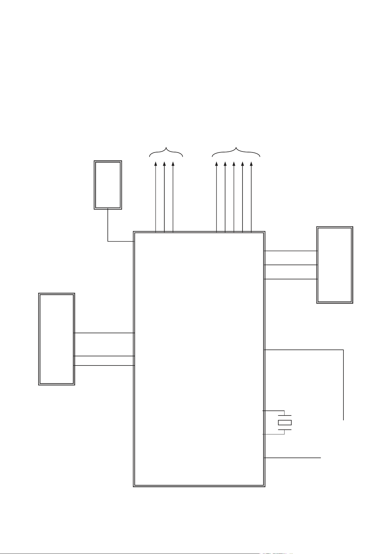
4. VIDEO & AUDIO Block Diagram
IC605
VIDEO 6dB
Amp
IC601
AUDIO DAC
(2CH)
IC301
AUDIO DAC
(5.1CH)
IC602 (OP Amp)
LPF&Buffer
IC701 Digital
POWER IC
IC303 Digital
POWER IC
IC304 Digital
POWER IC
CVBS
COMPONENT (R.G.B) / (Y.Pb.Pr )
SUPER VIDEO (Y/C)
(R.G.B) / (Y.Pb.Pr )
(Y/C)
DAC RESET
ACLK
SCL
SDA
DAC RESET
ACLK
SCL
SDA
ADATA1
ADATA2
ADATA3
A/V
JACK
MPEG
MPEG
MPEG
5.1CH BOARD
FRONT R
REAR R
FRONT L
REAR L
CENTER
WOOFER
AUDIO L
AUDIO R
ADATA3
❏ BLOCK DIAGRAM
2-5 2-6
2-7 2-8
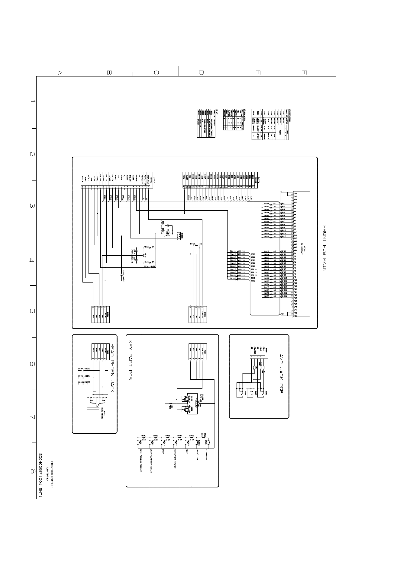
❏ SCHEMATIC DIAGRAMS
• FRONT SCHEMATIC DIAGRAM
2-9 2-10
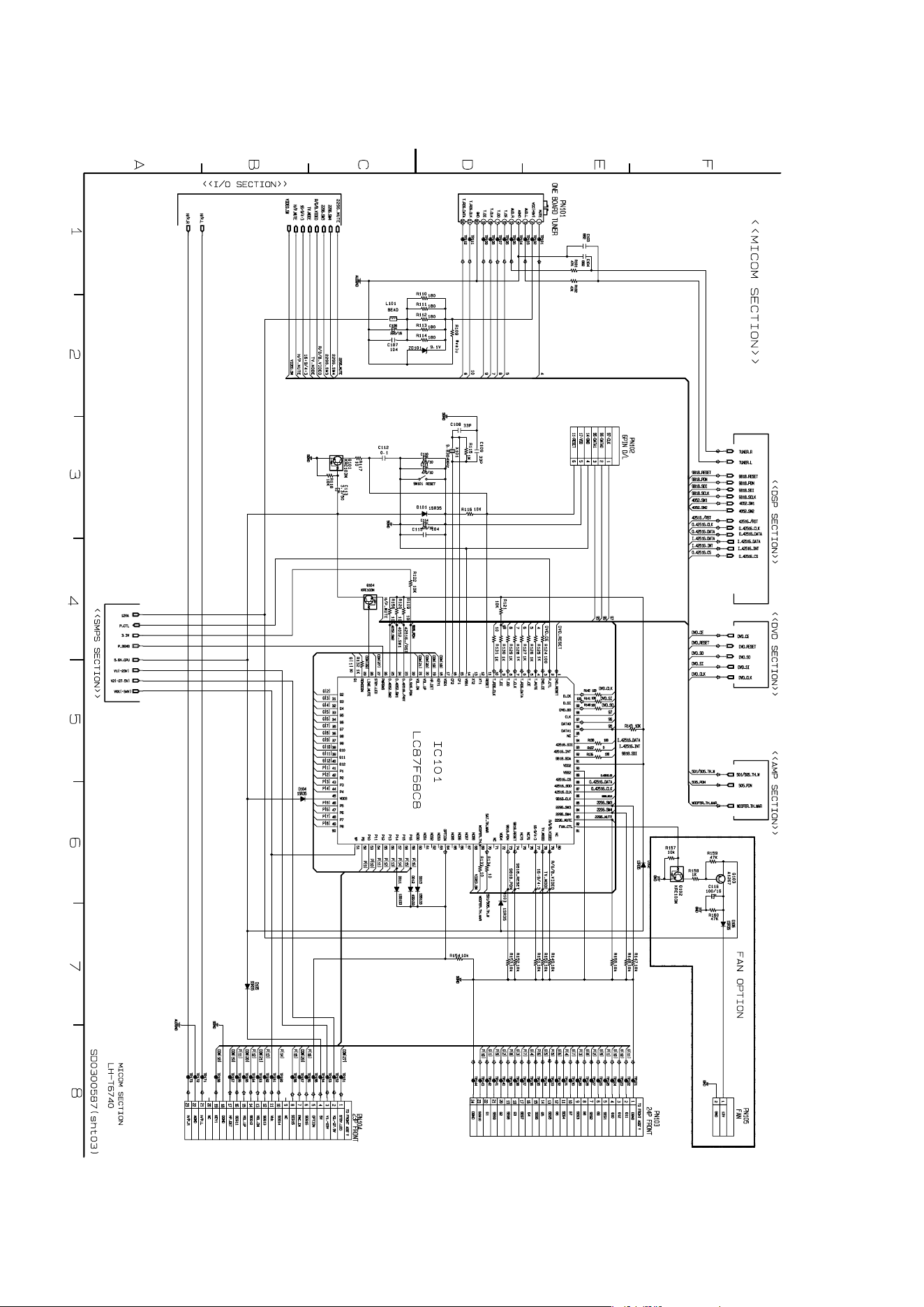
• MICOM SCHEMATIC DIAGRAM
2-11 2-12
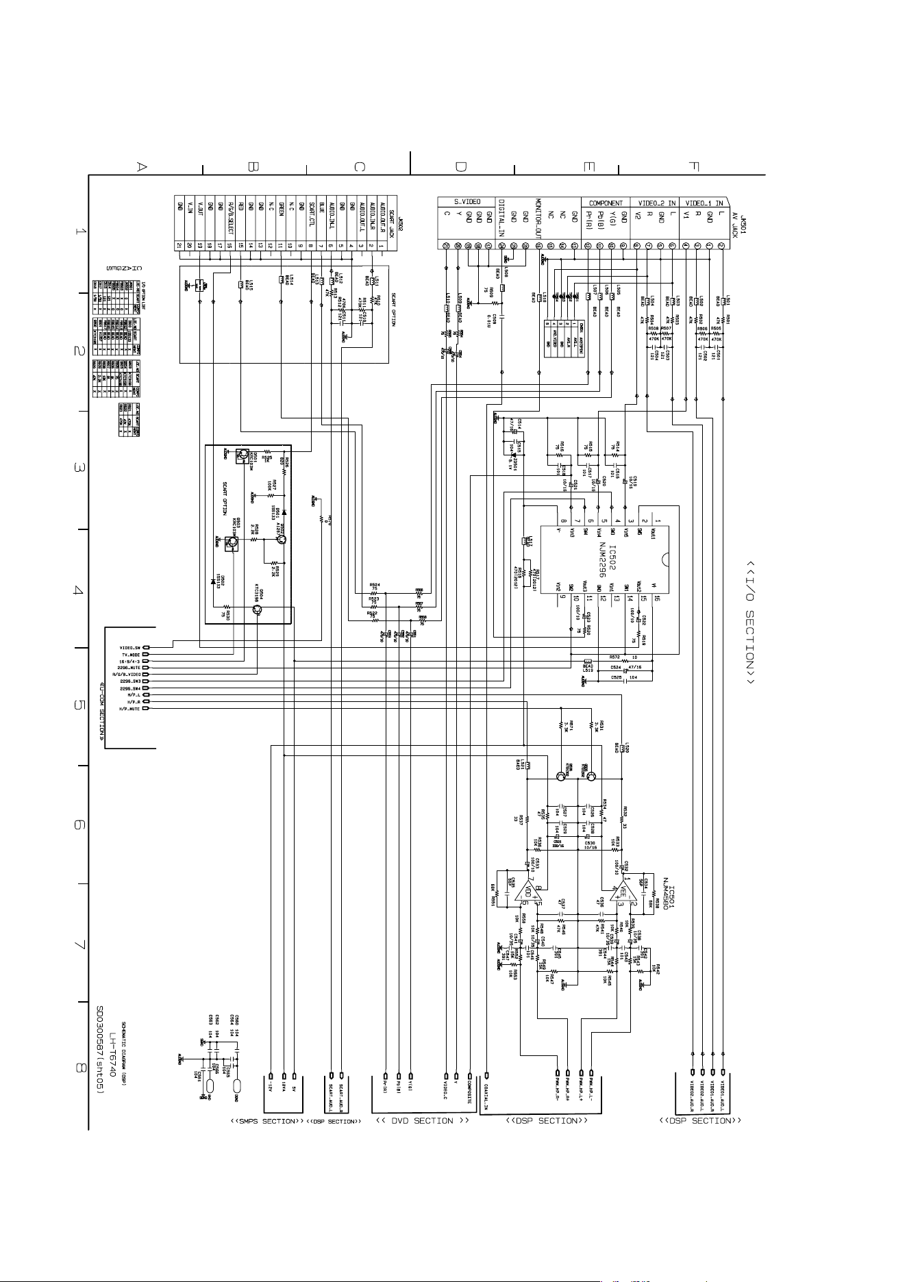
• I//O SCHEMATIC DIAGRAM
2-13 2-14
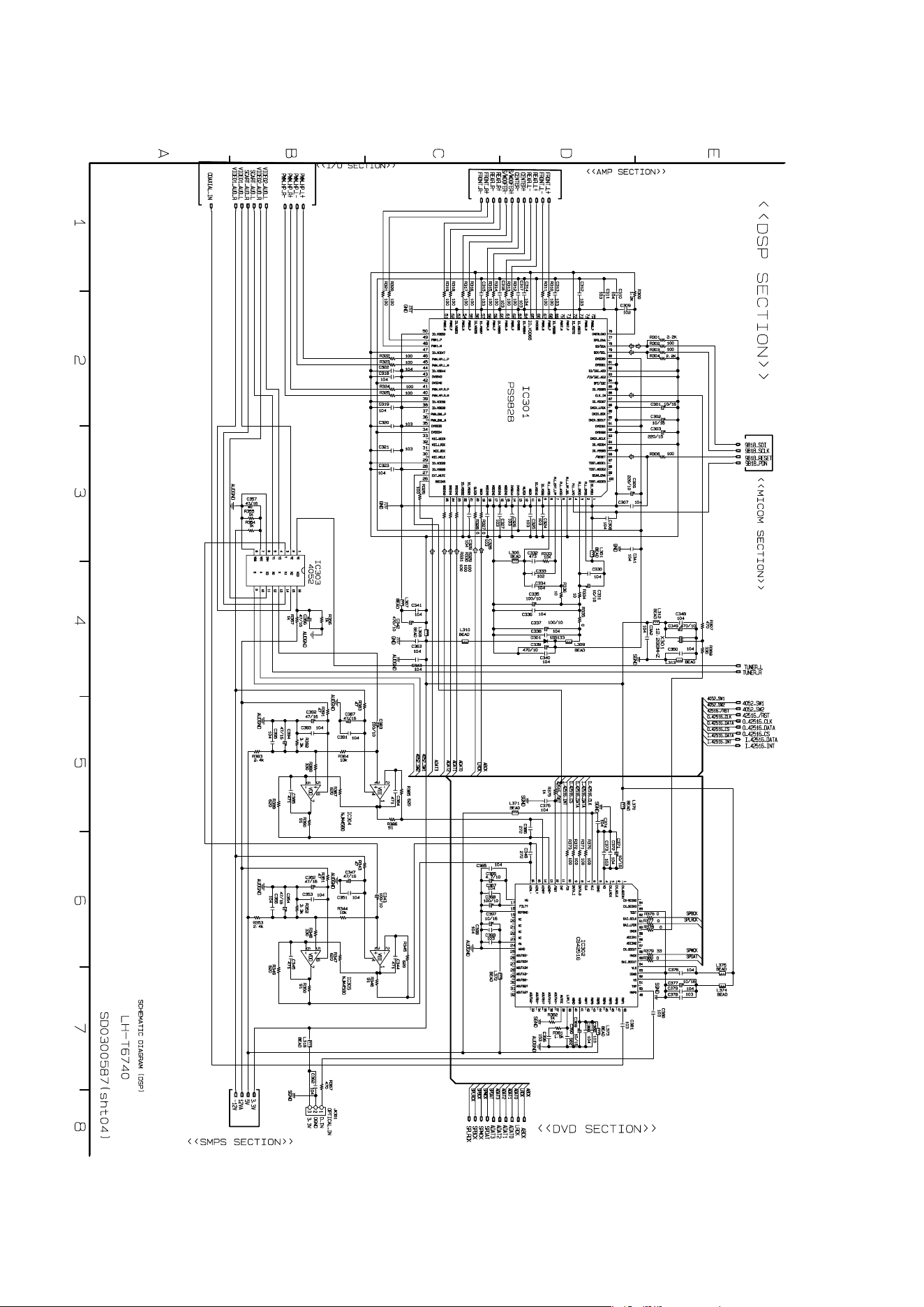
• DSP SCHEMATIC DIAGRAM
2-15 2-16
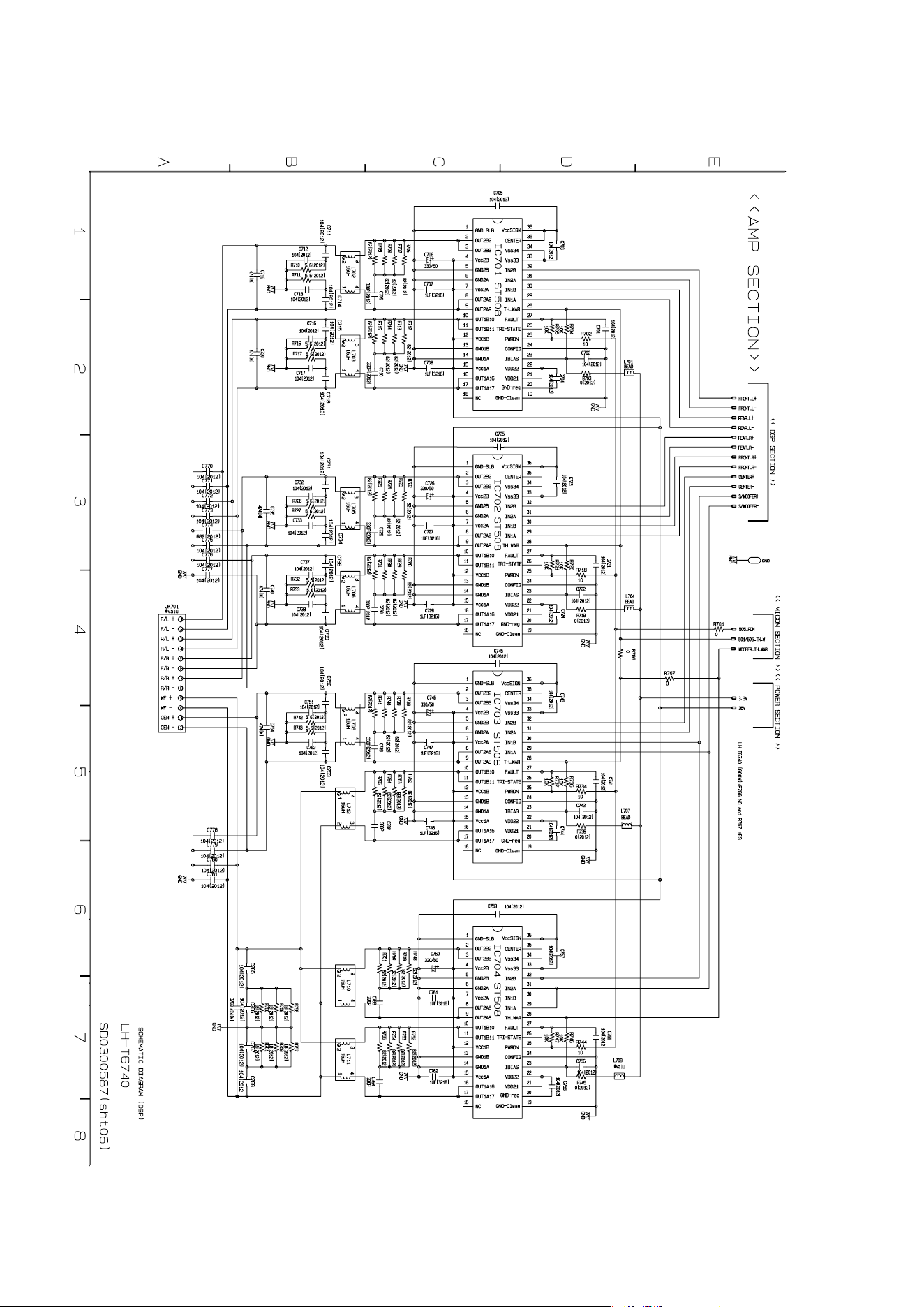
• AMP SCHEMATIC DIAGRAM
2-17 2-18
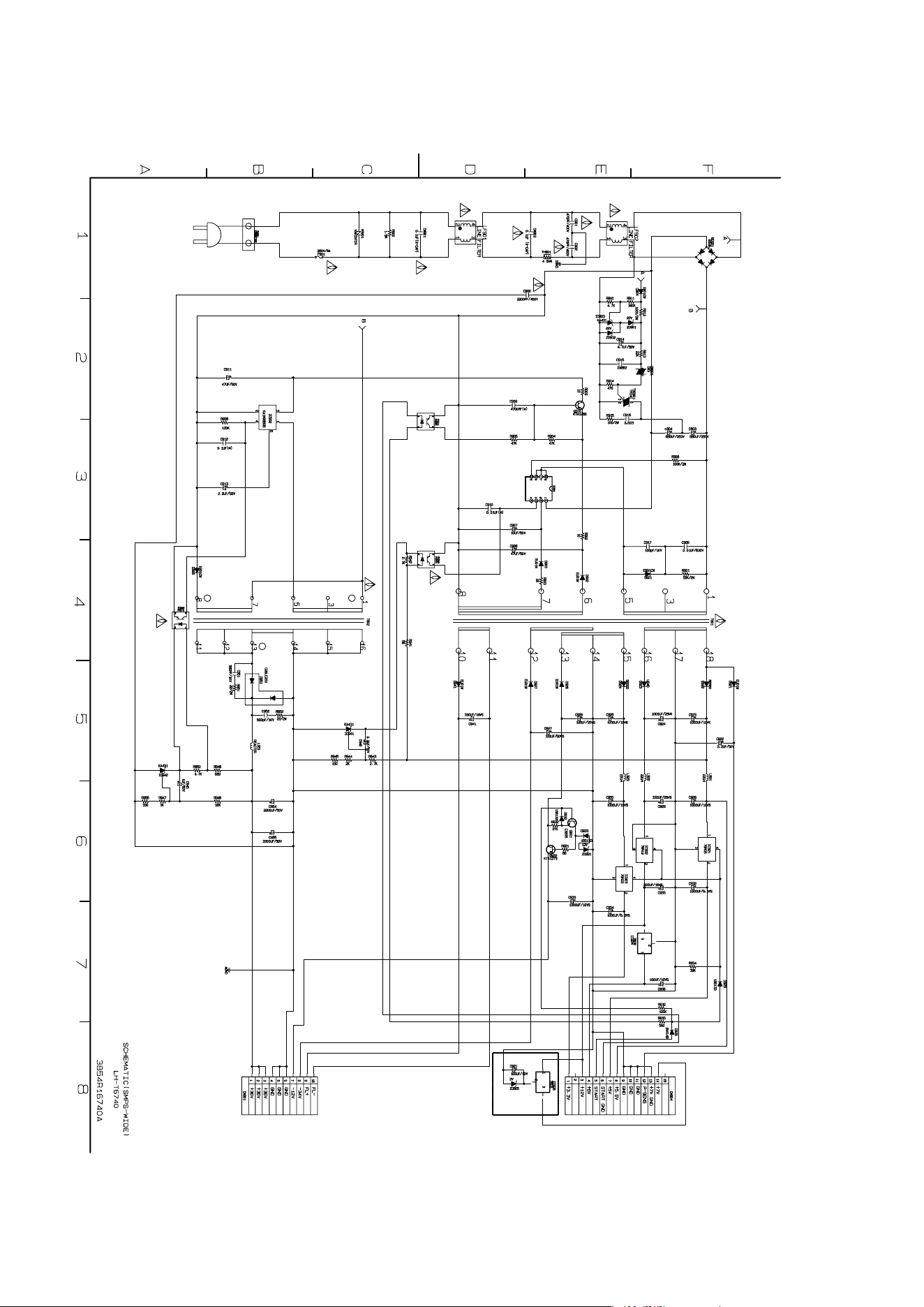
• SMPS-WIDE SCHEMATIC DIAGRAM
2-19 2-20
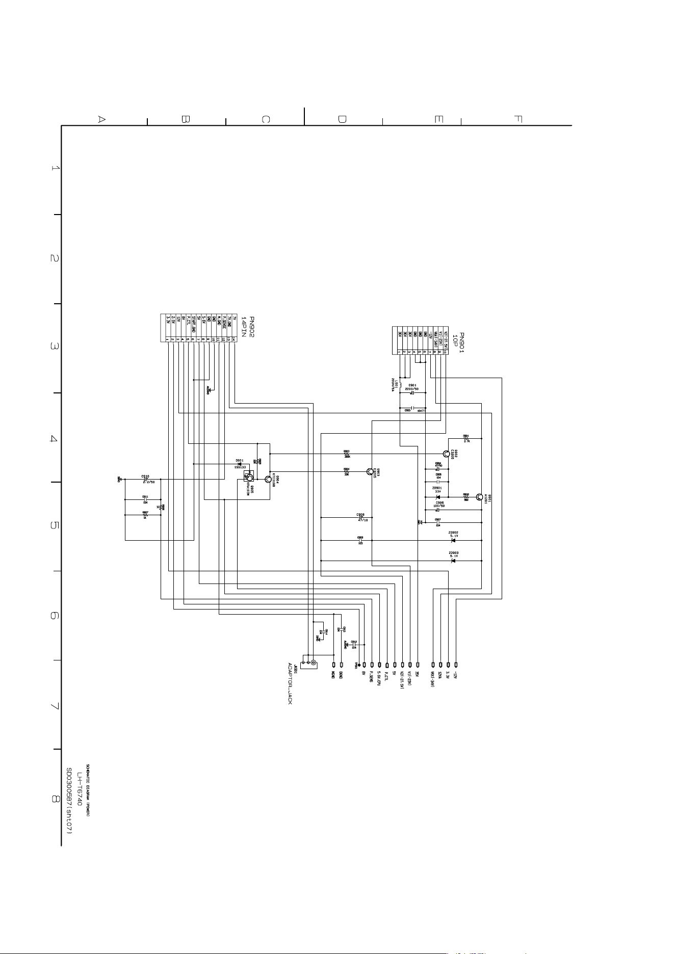
• POWER SCHEMATIC DIAGRAM
2-23 2-24
❏
PRINTED CIRCUIT DIAGRAMS
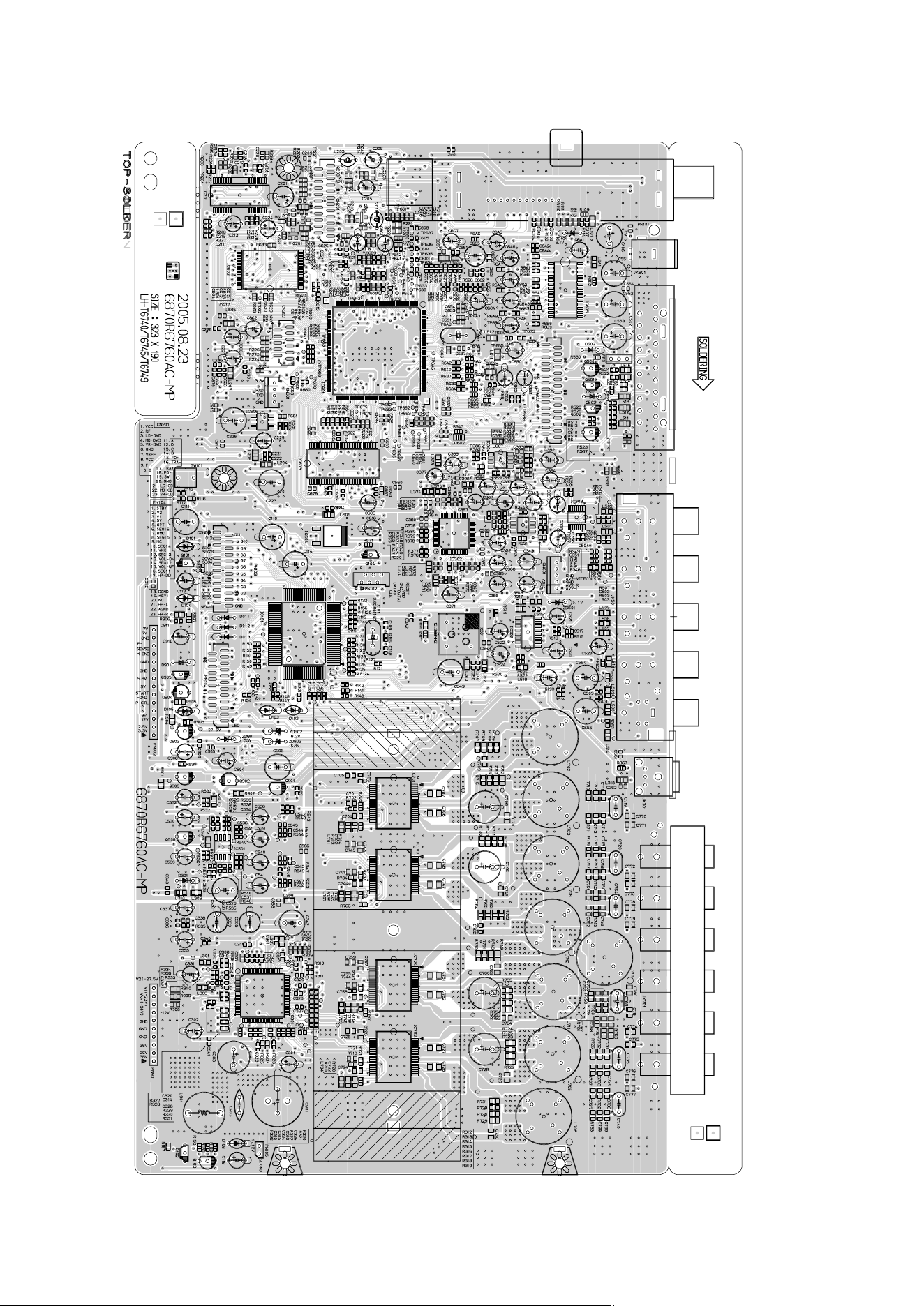
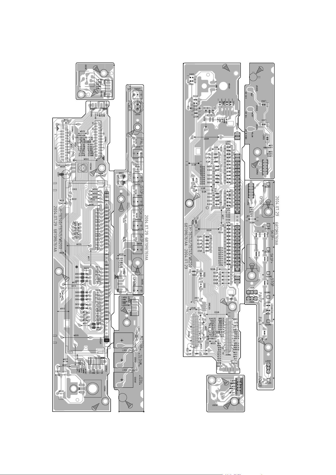
• MAIN P.C. BOARD (COMPONENT SIDE)
2-25 2-26
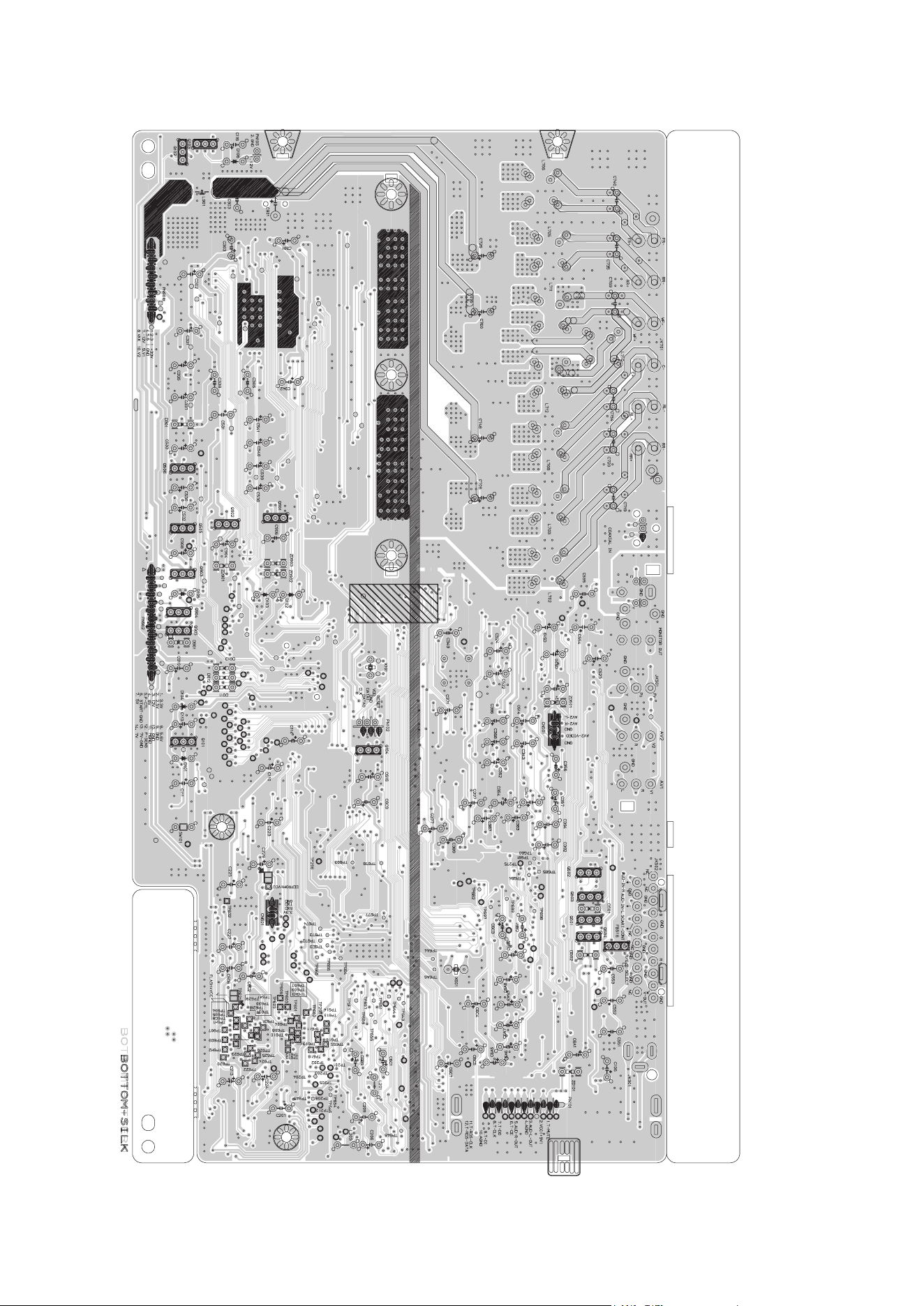
• MAIN P.C. BOARD (SOLDER SIDE)
2-21 2-22
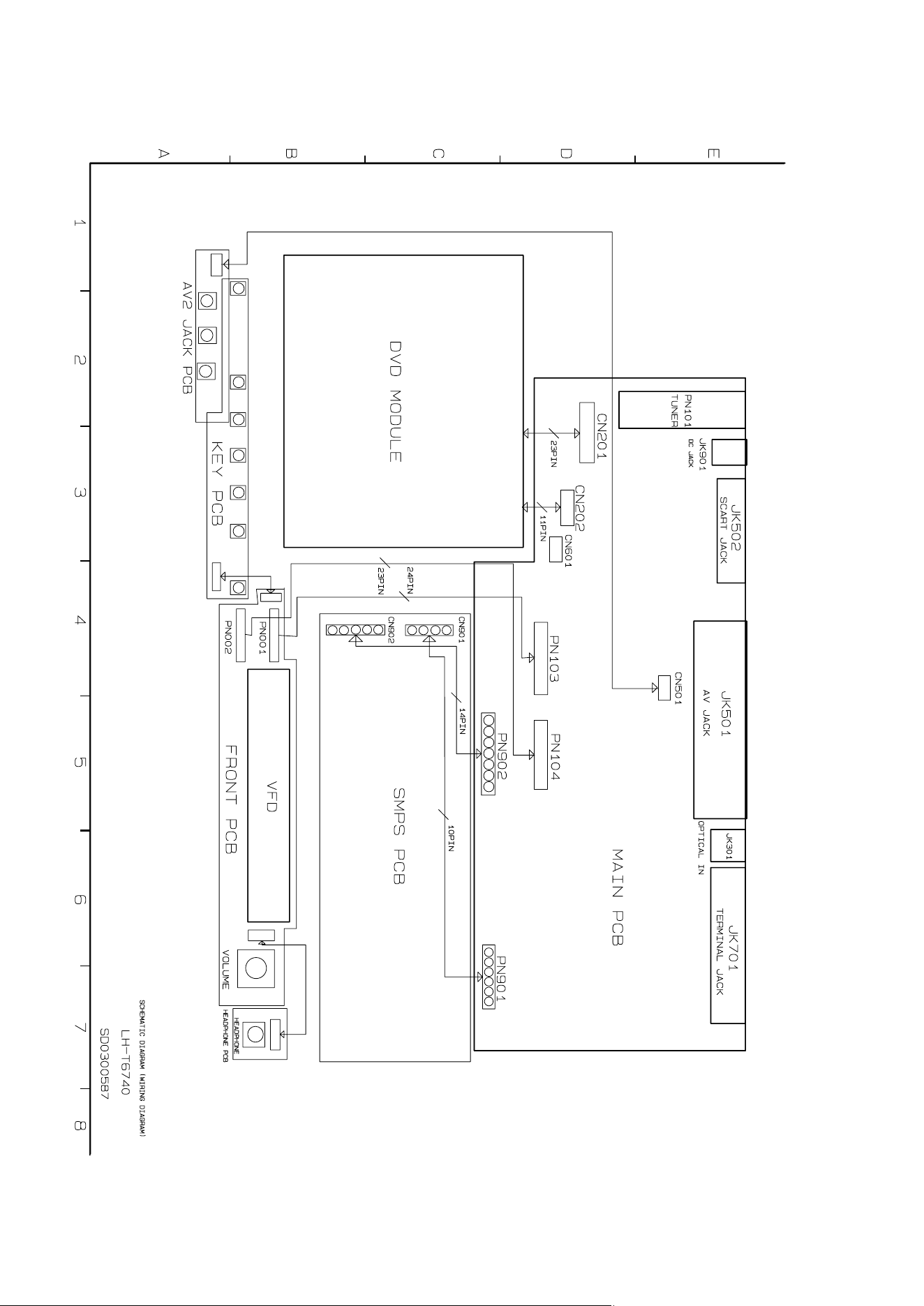
❏ WIRING DIAGRAMS
2-27 2-28
• FRONT P.C.BOARD (SOLDER SIDE)
• FRONT P.C.BOARD (COMPONENT SIDE)
2-29 2-30
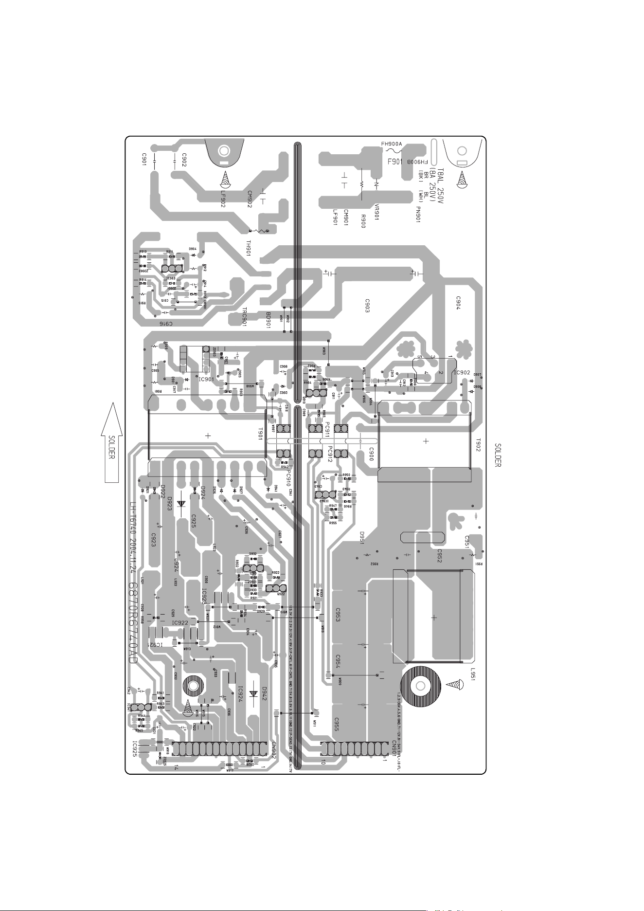
• POWER P.C.BOARD
2-31 2-32
3-25 3-26
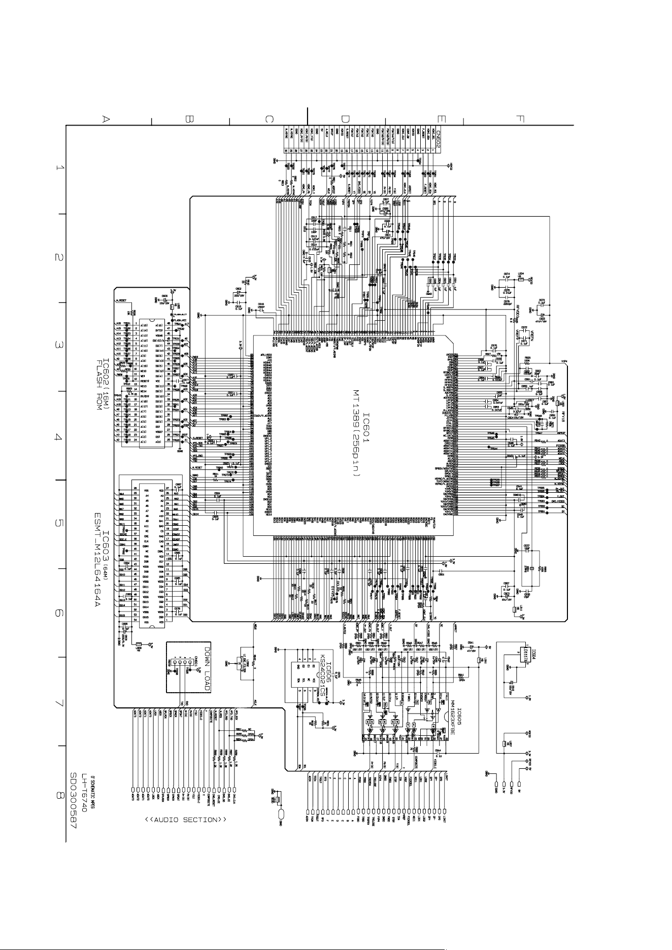
❏ DVD PART SCHEMATIC DIAGRAMS
• MPEG SCHEMATIC DIAGRAM

3-27 3-28
• SERVO SCHEMATIC DIAGRAM
4-1 4-2
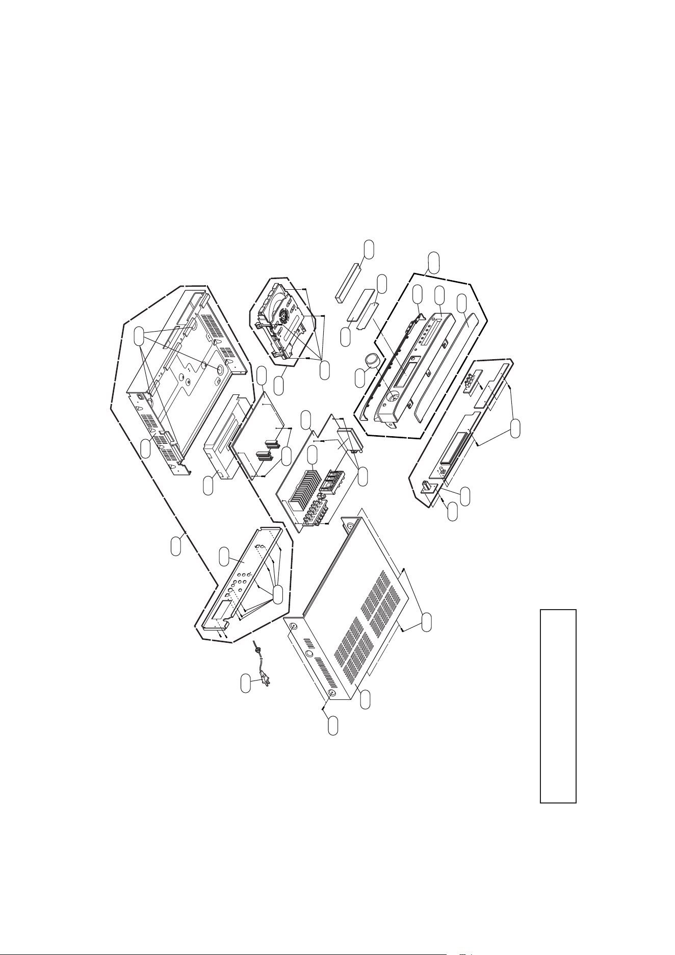
SECTION 4. EXPLODED VIEWS
❏ CABINET AND MAIN FRAME SECTION
NOTE) Refer to “SECTION 6 REPLACEMENT
PARTS LIST” in order to look for the
part number of each part.
T
U
1
0
1
A26
463
463
463
463
463
A46
283
280
A47
261
260
A44
250
A50
285
284
282
281
288
452
452
452
305
262
263
322
A43A
4-3 4-4
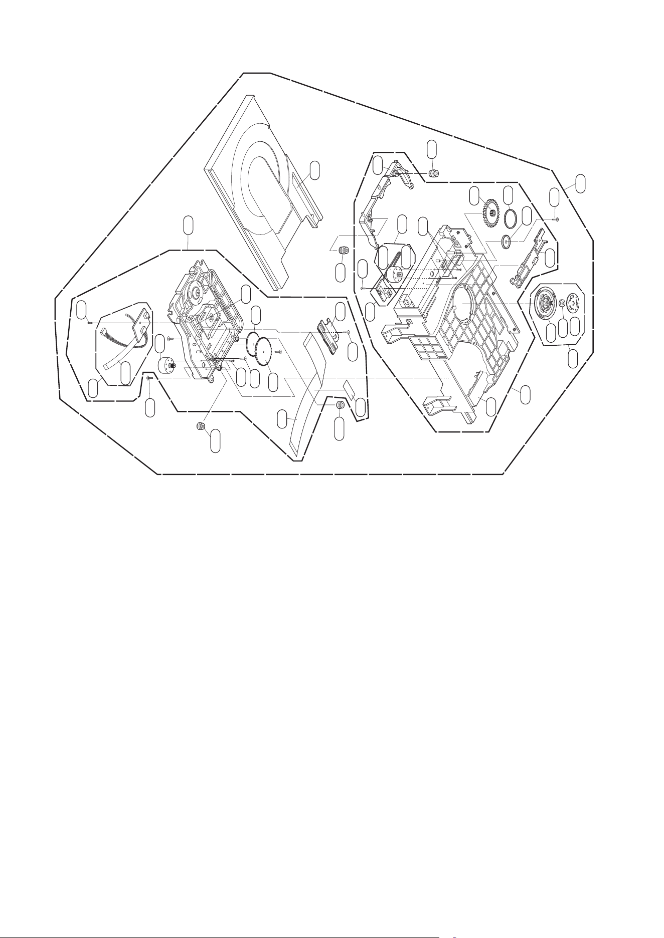
• DECK MECHANISM EXPLODED VIEW
A26
A01
001
002
003
A02
439
018
013
014
017
020
435
015
015B
015A
012
012
019
016
440440
026
012A
012A
A03
430
439
036
432
010
024
431
435
025
021
030
03
5
03
2
0
35
A
- 5-1 -
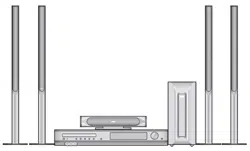
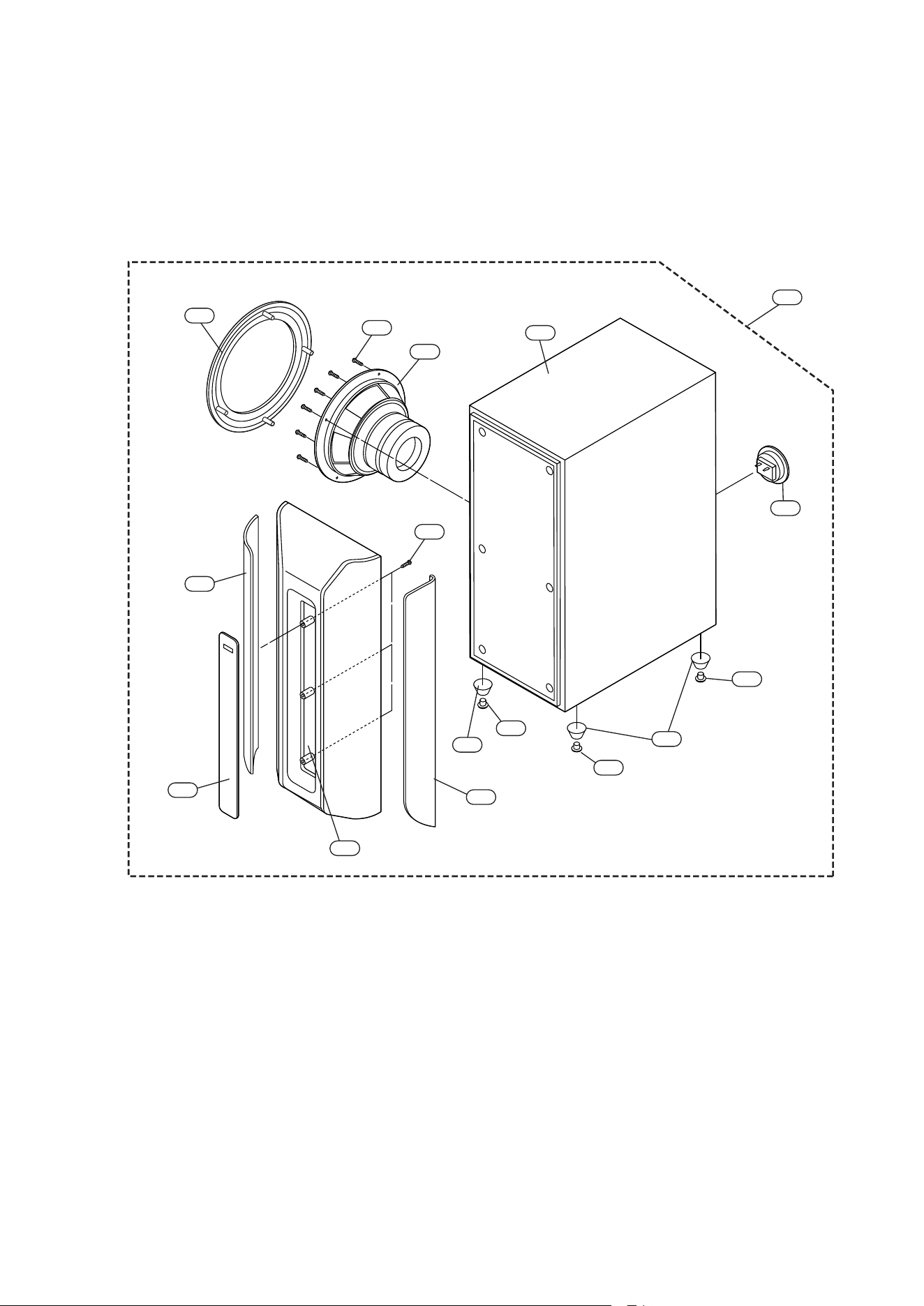
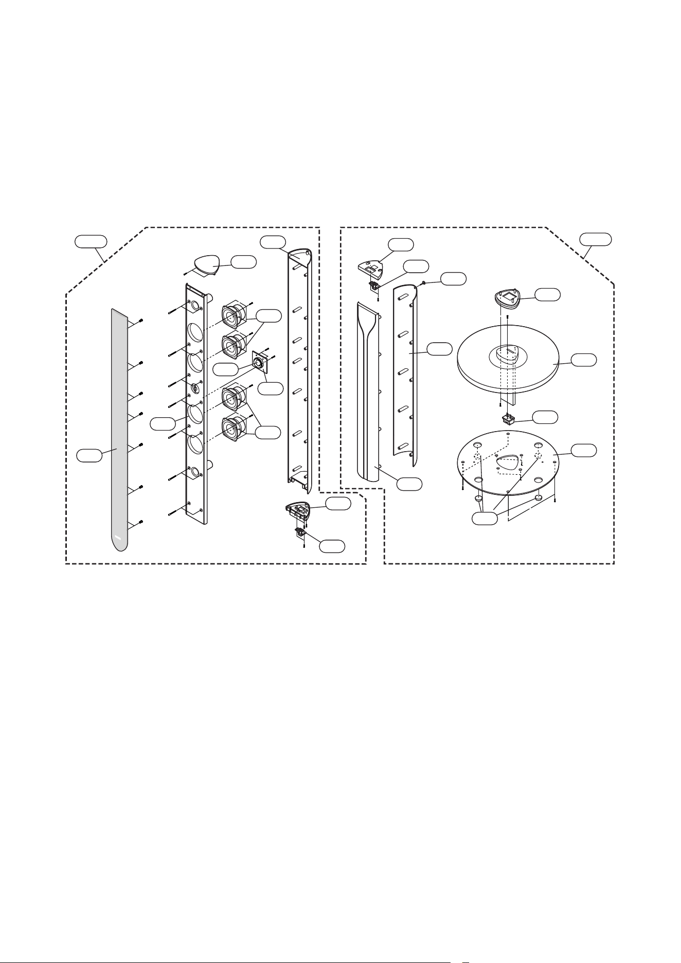
SECTION 5. SPEAKER PART
❏ MODEL: LHS-T6749W
658
654
660
A60
657
656
656
656
655
655
650
651
653
652
659
661
- 5-2 -
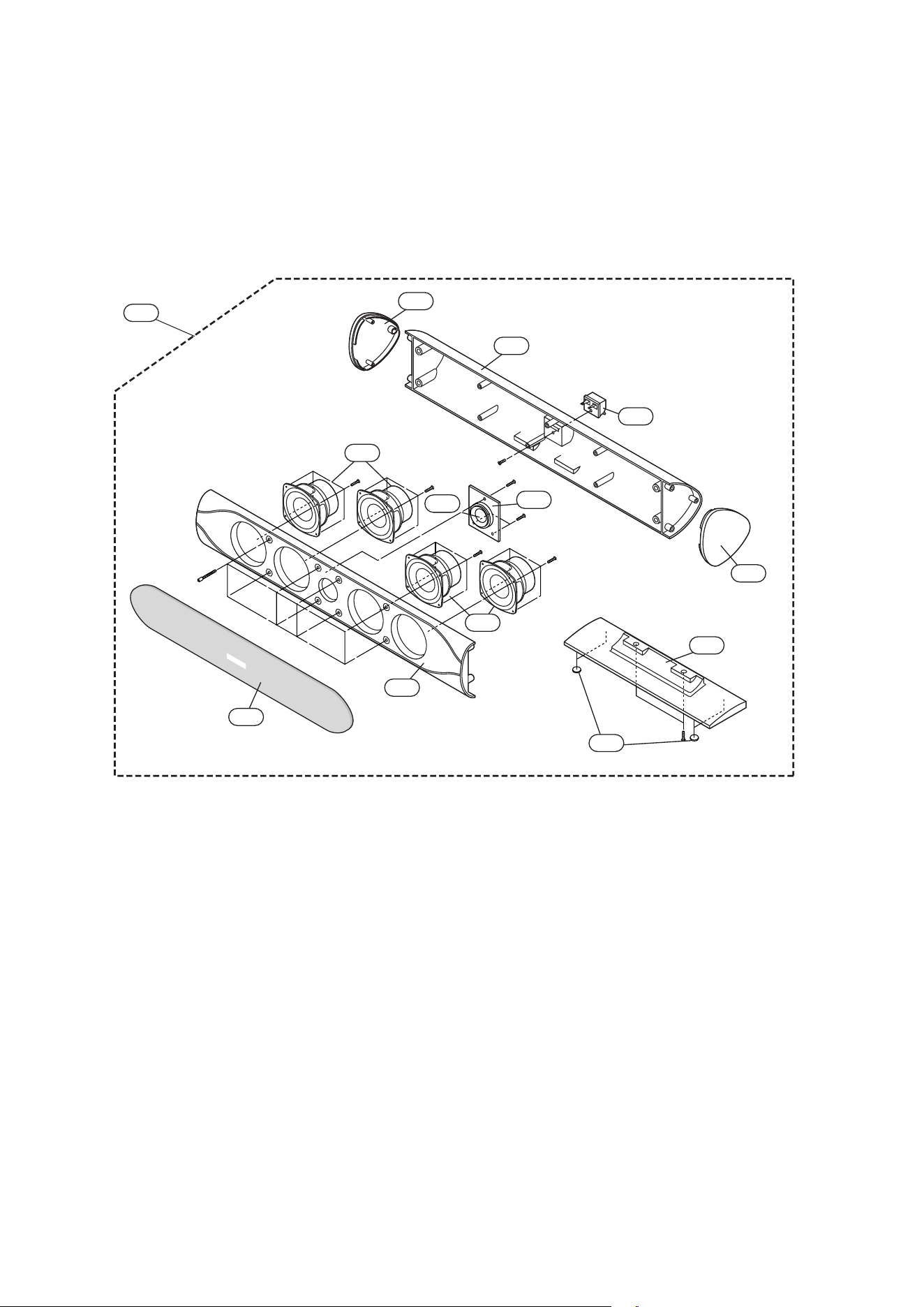
❏ MODEL: LHS-T6749C
A70
752
754
755
753
750
751
752
755
756
75
8
75
7
75
9
- 5-3 -
❏ MODEL: LHS-T6749T
A80A
A80B
850
851
852
853
854
853
855
856
857
858
861
868
860
859
863
864
862
867
865
866

- 5-4 -

MODEL : LH-T6749(A)/LHS-T6749C/LHS-T6749T/LHS-T6749W
SERVICE MANUAL
P/NO : 3829RDT050N NOVEMBER, 2006