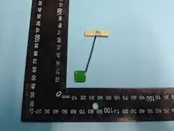

LM-M8188FU3
802.11n 72.
2Mbps WLAN
USB2.0 Module Specification
LawMate International Co.,Ltd.
Add: 3F, No.34, Lane 60, Wenhu St., Nei-Hu District, Taipei, Taiwan
1
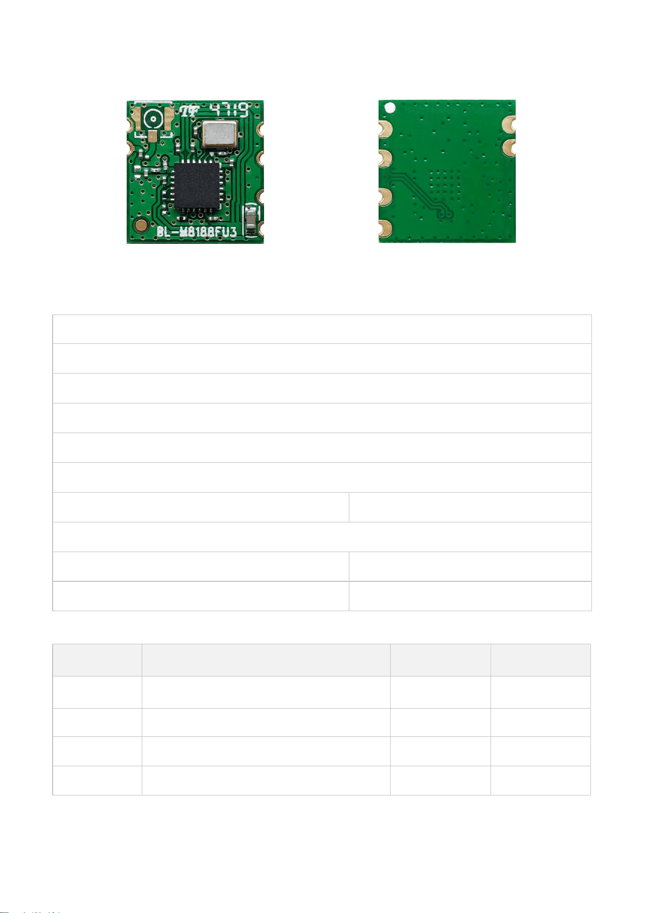
(Top View) (Bottom View)
Module Name: LM-M8188FU3
Module Type: 802.11b/g/n 72.2Mbps WLAN USB2.0 Module
Revision: V2.0.1
Customer Approval:
Company:
Title:
Signature: Date:
Approval:
Title:
Signature: Date:
Revision History
Revision Summary Release Date Revised By
2.0.0 Content optimization 2023-03-29 Qx
2.0.1 Official release 2024-03-11 Garry
2
1. Introduction
LM-M8188FU3 is a highly integrated 1T1R Single-band WLAN module. It compatible IEEE
802.11 b/g/n standard and provides the maximum PHY rate up to 72.2Mbps, offering
feature-rich wireless connectivity and delivering reliable, giving end users the highest cost
performance. On-chip 2M flash, extend to 4M, support transparent download, in buffer mode.
1.1 Features
Operating Frequencies: 2.4~2.4965GHz
Host Interface is USB 2.0
IEEE Standards: IEEE 802.11b/g/n
Wireless PHY rate can reach up to 72.2Mbps
Connect to external antenna through the half hole
Power Supply: DC3.3V±0.2V
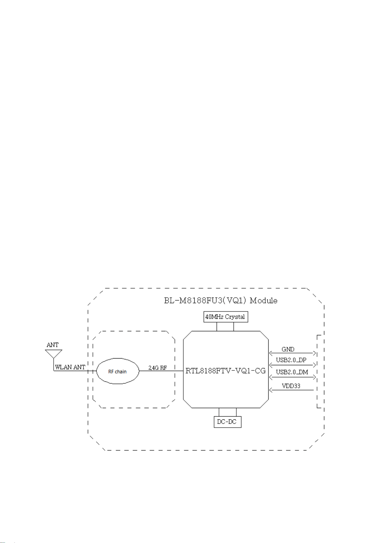
1.2 Block Diagram
3
1.3 General Specifications
Module Name LM-M8188FU3
Chipset RTL8188FTV-VQ1-CG
WLAN Standards IEEE802.11b/g/n
Host Interface USB2.0
Antenna Connect to external antenna through the half hole
Dimension 13.0*12.3*1.8mm (L*W*H)
Power Supply DC 3.3V±0.2V @ 500 mA(Max)
Operation Temperature -20℃ to +70℃
Operation Humidity 10% to 95% RH (Non-Condensing)
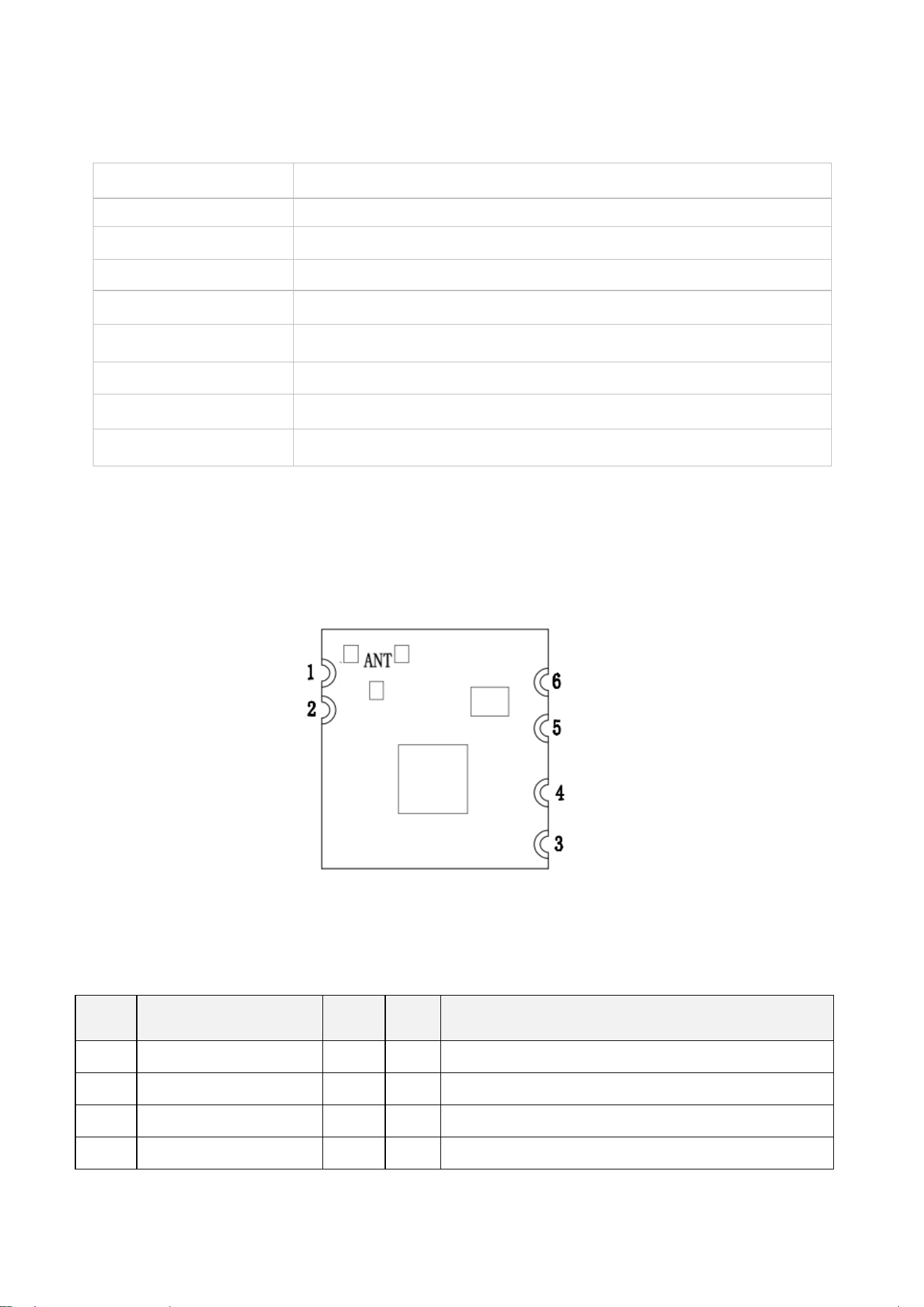
2. Pin Assignments
(Top View)
2.1 Pin Definition
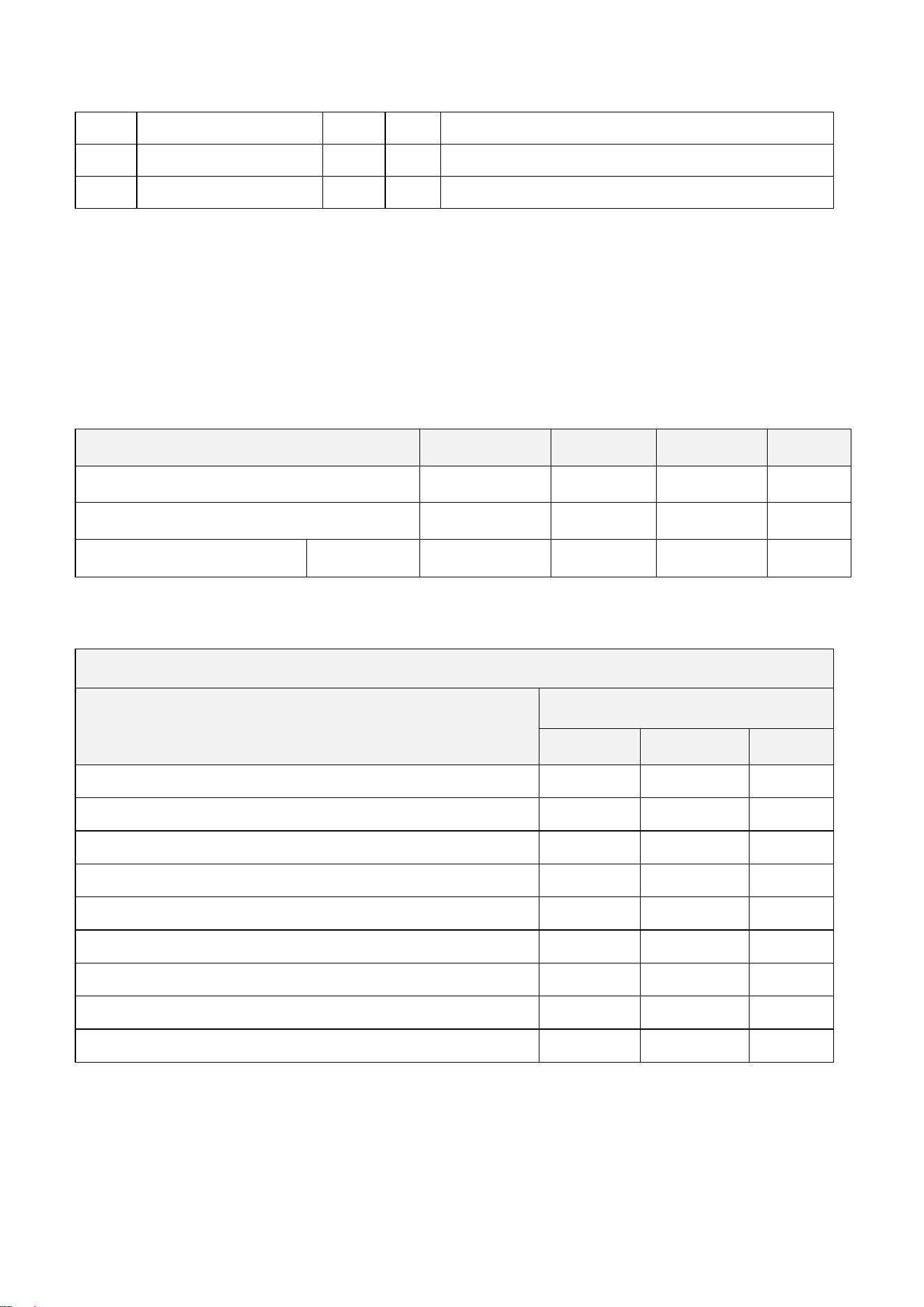
No. Pin Name Type Level Module Pin Description
1
GND RF
RF Ground connections
2
WLAN_ANT RF RF PAD for 2.4G WLAN ANT
3
VDD33 P
DC 3.3V Power Supply
4
USB2.0_DM A I/O
USB2.0 Transmitter/Receiver Differential Pair
4
5
USB2.0_DP A I/O
USB2.0 Transmitter/Receiver Differential Pair
6
GND P
Power Ground
ANT RF
NC (Reserved IPEX for 2.4G WLAN ANT)
P: Power or Ground; I/O: In/Output; I: Input; A I/O: Analog In/Output; AI: Analog Input;
AO: Analog Output; RF: Analog RF Port or RF Ground;
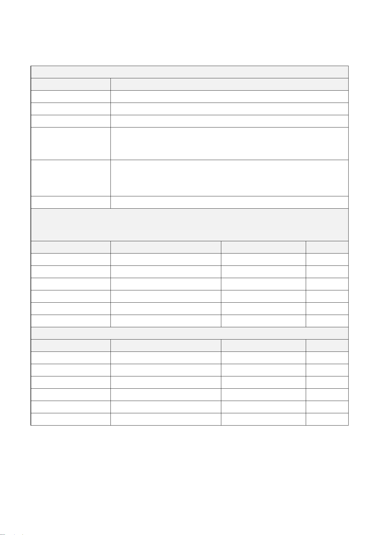
3. Electrical and Thermal Specifications
3.1 Recommended Operating Conditions
Parameters Min Typ Max Units
Ambient Operating Temperature -20 25 70 ℃
External Antenna VSWR 1.7 2 /
Supply Voltage VDD33 3.1 3.3 3.5 V
3.2 Current Consumption
Conditions : VDD33=3.3V ; Ta:25℃
Use Case
VDD33 Current (average)
Typ Max Units
WLAN Unassociated (Linux Driver) 40 60 mA
WLAN TRX Throughput(Linux Driver) 276 293 mA
2.4G 11b 1Mbps TX @17dBm (RF-Test ) 272 331 mA
2.4G 11b 11Mbps TX@17dBm (RF-Test) 305 320 mA
2.4G 11g 6Mbps TX @17dBm (RF-Test ) 280 292 mA
2.4G 11g 54Mbps TX @15dBm (RF-Test) 270 285 mA
2.4G 11n HT20-MCS0 TX @17dBm (RF-Test) 277 290 mA
2.4G 11n HT20-MCS7 TX @15dBm (RF-Test) 272 285 mA
2.4G 11n HT20-MCS7 RX (RF-Test) 59 70 mA
5
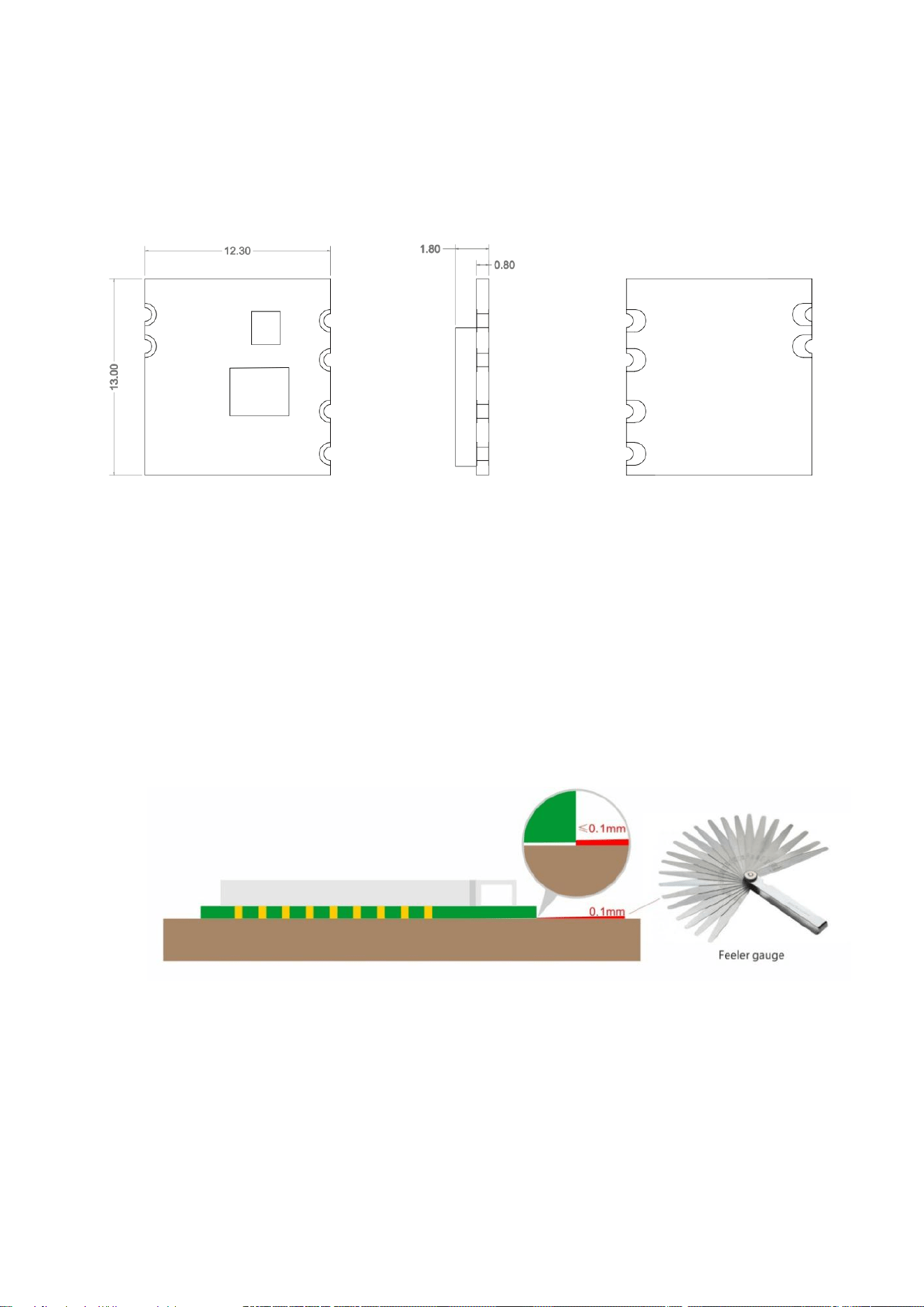
4. WLAN RF Specifications
Conditions : VDD33=3.3V ; Ta:25℃
Features Description
WLAN Standard IEEE 802.11b/g/n
Frequency Range 2.4~2.4965GHz
Channels Ch1~Ch14 (For 20MHz Channels)
Modulation
802.11b (DSSS): DBPSK, DQPSK, CCK;
802.11g (OFDM): BPSK, QPSK, 16QAM, 64QAM;
802.11n (OFDM): BPSK, QPSK, 16QAM, 64QAM;
Data Rate
802.11b: 1, 2, 5.5, 11Mbps;
802.11g: 6, 9, 12, 18, 24, 36, 48, 54Mbps;
802.11n (HT20): MCS0~MCS7(1T1R_SISO) 6.5~72.2Mbps;
Frequency Tolerance ≦±20ppm
2.4G Transmitter Specifications( TX power of some rates is calibrated, customers can define the target TX
power of other rates by modifying configuration file of the driver software. Customers must define the TX
power same or lower than recommended Target TX Power as below)
TX Rate TX Power(dBm) TX Power Tolerance(dBm) EVM(dB)
802.11b@1Mbps Recommended Target TX Power :17
±1
≦-10
802.11b@11Mbps Calibrated TX Power :17
±1
≦-15
802.11g@6Mbps
Recommended Target TX Power :16
±1 ≦-10
802.11g@54Mbps Calibrated TX Power :16 ±1 ≦-25
802.11n@HT20_MCS0
Recommended Target TX Power :16
±1 ≦-10
802.11n@HT20_MCS7 Calibrated TX Power :16 ±1 ≦-28
2.4G Receiver Specifications
RX Rate Min Input Level(Typ,dBm) Max Input Level(Typ,dBm) PER
802.11b@1Mbps -92 -10 < 8%
802.11b@11Mbps -86
-10
< 8%
802.11g@6Mbps -90 -15 < 10%
802.11g@54Mbps -72
-15
< 10%
802.11n@HT20_MCS0 -88 -15 < 10%
802.11n@HT20_MCS7 -72
-15
< 10%
6
5.Mechanical Specifications
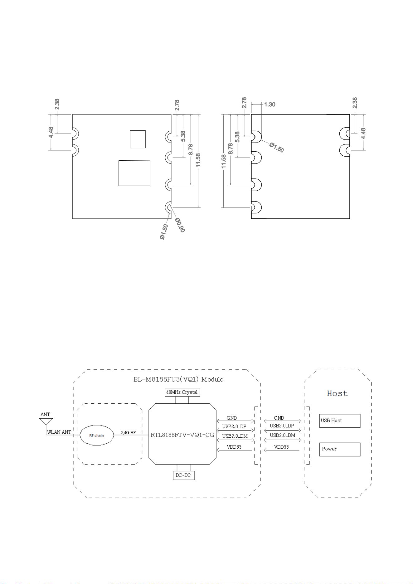
5.1 Module Outline Drawing
(Top View) (Side View) (Bottom View)
Module dimension: 13.0*12.3*1.8mm (L*W*H; Tolerance: ±0.3mm_L/W, ±0.2mm_H)
Module Bow and Twist:≤0.1mm
7
5.2 Mechanical Dimensions
(Top View) (Bottom View)
6. Application Information
6.1 Typical Application Circuit

8
6.2 HW Application Note
6.2.1 VDD33 Power requirement:
A、DC 3.1~3.5V & Ripple Voltage <100mV power supply input, Maximum Peak current≥0.5A.
B、For achieve fast transient response,a current mode buck converter recommended.
C、On customer's motherboard, use 10uF and 100nF MLCC capacitors close to the module`s VDD33 Pin for
power input decoupling. Each GND Pin has three close vias to ensure connectivity and thermal conductivity.
6.2.2 USB interface Design Guidelines:
A、The module provides a USB device interface which is compatible with USB2.0 specification, High-Speed
mode supports data transmission rate up to 480Mbps.
B、On customer's motherboard, PCB traces of the USB high-speed signal pair should be maintain 90
Ω
differential impedance, structure of“Differential Coated Coplanar Waveguide With Ground”with the
advantages of impedance control and GND surrounding isolation interference may be an ideal choice. To
avoid interference, USB signal pair must be far away from power, RF and other signals, GND copper can be
used to surround and isolate them.
C、PCB traces of the USB high-speed signal pair as short as possible, as far away from other signal as possible,
minimize the length mismatch of signal pair, avoid layer change and maintain a complete reference layer to
reduces signal reflections and impedance changes.
D、If It is necessary to change layers for USB signal pair routing, use GND vias close to signal pair`s vias as the
shortest return path.
6.2.3 RF Path Design Guidelines:
A、On customer's motherboard, keep complete GND copper area under and around the module, do not route
Power, RF, USB and other signals there to avoid interfering with the module causing RF performance
derating problem.
B、PCB traces of the RF path as short as possible, as far away from other signal as possible, avoid layer change,
and should be maintain continuous 50
Ω
characteristic impedance, structure of“Coated Coplanar
Waveguide With Ground”with the advantages of impedance control and GND surrounding isolation
interference may be an ideal choice. It is necessary to maintain a complete GND reference layer below the
RF path area.
C、RF Pin and antenna PAD/RF connector PAD on customer's motherboard are significantly wider than PCB
traces of the RF path, which will cause RF impedance discontinuity. To improve this problem, in addition to
adjusting the local impedance of these PADs, a“π” circuit can be reserved near the antenna/RF connector
which can match both RF path impedance and antenna impedance.
9
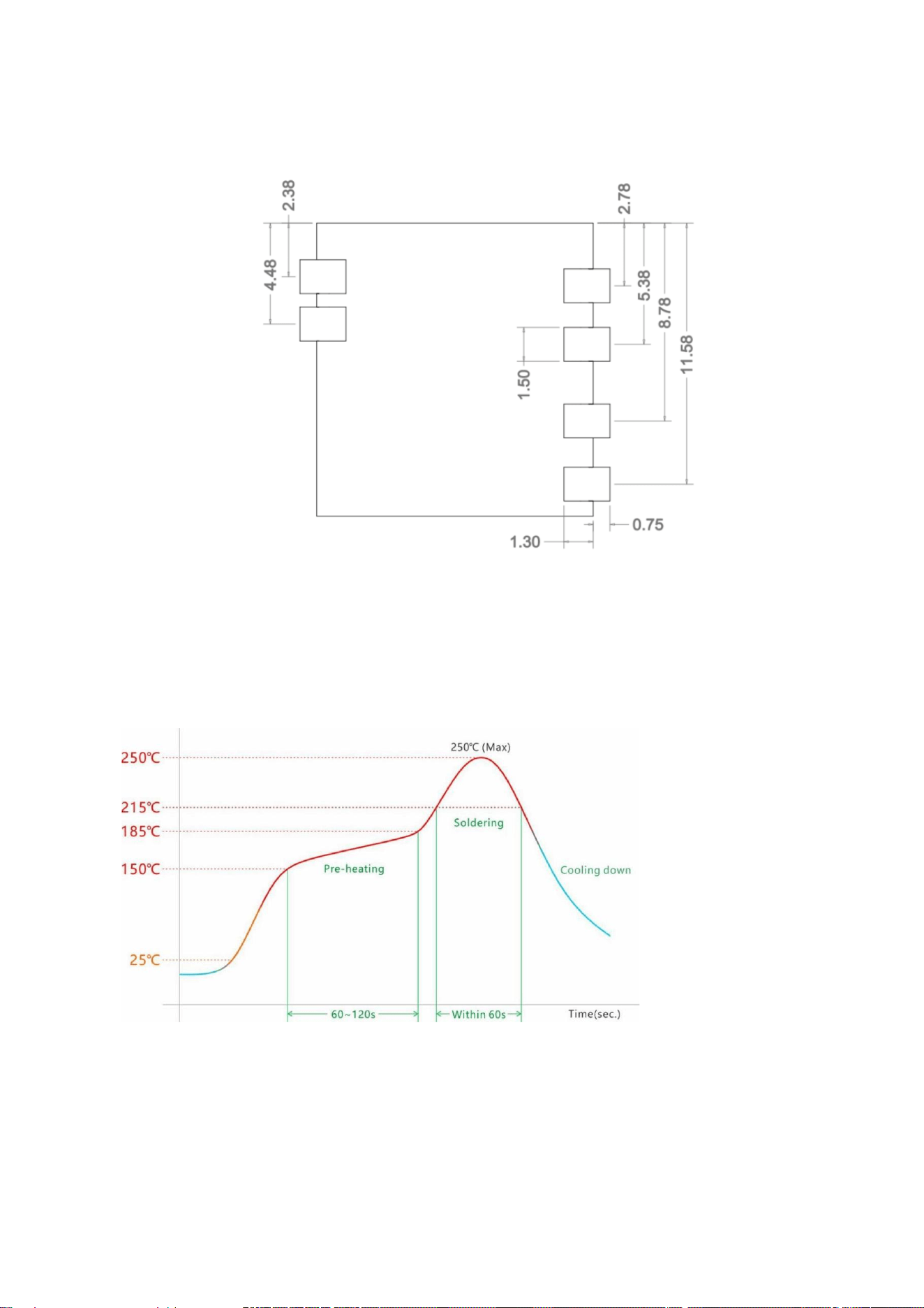
6.3 Recommend PCB Layout Footprint
(Design Unit: mm)
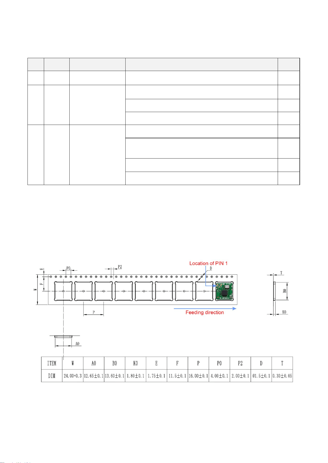
6.4 Reflow Soldering Standard Conditions
Please use the reflow within 2 times.
Set up the highest temperature within 250℃.
10
7. Key Components Of Module
8. Package and Storage Information
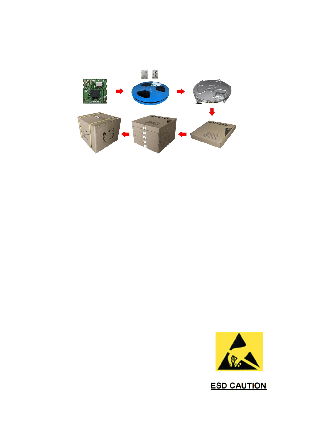
8.1Package Dimensions
No. Parts Specification Manufacturer Note
1 Chipset RTL8188FTV-VQ1-CG
Realtek Semiconductor Corp.
2 PCB LM-M8188FU3
ShenZhen Tie Fa Technology Limited
SHEN ZHEN QILI ELECTRON CO.,LTD
MILLION SOURCE PRINTED CIRCUIT BOARD CO.,LTD
3 Crystal 40MHz-3225
Chengde oscillator Electronic Technology CO.,LTD
HUBEI TKD CRYSTAL ELECTRONIC SCIENCE AND TECHNOLOGY
CO.,LTD
SHENZHEN KAIYUEXIANG ELECTRONICS CO.,LTD
JinHua East Crystal Electronic CO.,LTD
11
Package specification:
1. 2,000 modules per roll and 10,000 modules per box.
2. Outer box size: 37.5*36*29cm.
3. The diameter of the blue environment-friendly rubber plate is 13 inches, with a total thickness of 28mm (with a
width of 24mm carrying belt).
4. Put 1 package of dry agent (20g) and 1 humidity card in each anti-static vacuum bag.
5. Each carton is packed with 5 boxes.
8.2 Storage Conditions
Absolute Maximum Ratings:
Storage temperature: -40℃ to +85℃,
Storage humidity: 10% to 95(Non-Condensing)
Recommended Storage Conditions:
Storage temperature: 5℃ to +40℃,
Storage humidity: 20% to 90% RH
Please use this Module within 12month after vacuum-packaged.
The Module shall be stored without opening the packing.
After the packing opened, the Module shall be used within 72hours.
When the color of the humidity indicator in the packing changed,
The Module shall be baked before soldering.
Baking condition: 60℃, 24hours, 1time.
ESD Sensitivity:
ESD Protection: 2KV(HBM ,Maximum rating)
The Module is a static-sensitive electronic device.
Do not operate or store near strong electrostatic fields.
Take proper ESD precautions!

FCC Statement
This device complies with part 15 of the FCC rules. Operation is subject to the following two conditions: (1)
this device may not cause harmful interference, and (2) this device must accept any interference received,
including interference that may cause undesired operation.
Changes or modifications not expressly approved by the party responsible for compliance could void the user’
s authority to operate the equipment.
NOTE: This equipment has been tested and found to comply with the limits for a Class B digital device, pursua
nt to part 15 of the FCC Rules. These limits are designed to provide reasonable protection against harmful inte
rference in a residential installation. This equipment generates uses and can radiate radio frequency energy a
nd, if not installed and used in accordance with the instructions, may cause harmful interference to radio com
munications. However, there is no guarantee that interference will not occur in a particular installation. If this
equipment does cause harmful interference to radio or television reception, which can be determined by turn
ing the equipment off and on, the user is encouraged to try to correct the interference by one or more of the
following measures:
‐
Reorient or relocate the receivingantenna.
‐ Increase the separation between the equipment and receiver.
‐
Connect the equipment into an outlet on a circuit different from that to which the receiver is connected.
‐Consult the dealer or an experienced radio/TV technician for help important announcement
Important Note:
Radiation Exposure Statement
This equipment complies with FCC radiation exposure limits set forth for an uncontrolled environment. This
equipment should be installed and operated with minimum distance 20cm between the radiator and your
body.
This transmitter must not be co-located or operating in conjunction with any other antenna or transmitter.
Country Code selection feature to be disabled for products marketed to the US/Canada.
This device is intended only for OEM integrators under the following conditions:
1. The antenna must be installed such that 20 cm is maintained between the antenna and users, and
2. The transmitter module may not be co-located with any other transmitter or antenna,
As long as the conditions above are met, further transmitter testing will not be required. However, the OEM
integrator is still responsible for testing their end-product for any additional compliance requirements
required with this module installed.
Important Note:
In the event that these conditions cannot be met (for example certain laptop configurations or co-location
with another transmitter), then the FCC authorization is no longer considered valid and the FCC ID cannot be
used on the final product. In these circumstances, the OEM integrator will be responsible for re-evaluating the
end product (including the transmitter) and obtaining a separate FCC authorization.
End Product Labeling
The final end product must be labeled in a visible area with the following"
Contains FCC ID: 2AHTX-LM-M8188FU3 "
Manual Information to the End User
The OEM integrator has to be aware not to provide information to the end user regarding how to install or
remove this RF module in the user’s manual of the end product which integrates this module.
The end user manual shall include all required regulatory information/warning as show in this manual.
Integration instructions for host product manufacturers according to KDB 996369 D03
OEM Manual v01r01
2.2
List of applicable FCC rules
CFR 47 FCC PART 15 SUBPART C has been investigated. It is applicable to the modular transmitter
2.3
Specific operational use conditions
This module is stand-alone modular. If the end product will involve the Multiple simultaneously transmitting
condition or different operational conditions for a stand-alone modular transmitter in a host, host manufacturer have
to consult with module manufacturer for the installation method in end system.
2.4
Limited module procedures
Not applicable
2.5
Trace antenna designs
Not applicable
2.6
RF exposure considerations
This equipment complies with FCC radiation exposure limits set forth for an uncontrolled environment. This
equipment should be installed and operated with minimum distance 20cm between the radiator & your body.
2.7
Antennas
This radio transmitter
FCC ID:2AHTX-LM-M8188FU3
has been approved by Federal Communications
Commission to operate with the antenna types listed below, with the maximum permissible gain indicated. Antenna
types not included in this list that have a gain greater than the maximum gain indicated for any type listed are strictly
prohibited for use with this device.
Antenna No.
Model No.
of antenna:
Type of antenna:
Gain of the antenna
(Max.)
Frequency
range:
2.4G WIFI
/
FPC Antenna
2.5
2402-2480MHz
2.8
Label and compliance information
The final end product must be labeled in a visible area with the following" Contains FCC ID:2AHTX-LM-M8188FU3
".
2.9
Information on test modes and additional testing requirements
Host manufacturer is strongly recommended to confirm compliance with FCC requirements for the transmitter when
the module is installed in the host.
2.10
Additional testing, Part 15 Subpart B disclaimer
Host manufacturer is responsible for compliance of the host system with module installed with all other applicable
requirements for the system such as Part 15 B.
2.11
Note EMI Considerations
Host manufacture is recommended to use D04 Module Integration Guide recommending as "best practice" RF
design engineering testing and evaluation in case non-linear interactions generate additional non-compliant limits
due to module placement to host components or properties.
2.12
How to make changes
This module is stand-alone modular. If the end product will involve the Multiple simultaneously transmitting
condition or different operational conditions for a stand-alone modular transmitter in a host, host manufacturer have
to consult with module manufacturer for the installation method in end system. According to the KDB 996369 D02
Q&A Q12, that a host manufacture only needs to do an evaluation (i.e., no C2PC required when no emission
exceeds the limit of any individual device (including unintentional radiators) as a composite. The host manufacturer
must fix any failure.