UBXDOC-465451970-3820 - R01
C2-Restricted www.u-blox.com
JODY-B1 series System
Integration Manual
Host-based automotive modules with Dual-Mode
Bluetooth®
System integration manual
Abstract
Targeted towards hardware and software application engineers, this document describes how to
integrate JODY-B1 modules in application products and explains the hardware design-in, software,
component handling, regulatory compliance, and production testing. It also lists the external
antennas approved for use with the module.

JODY-B1 series System Integration Manual - System integration manual
UBXDOC-465451970-3820 - R01 Document information Page 2 of 44
C2-Restricted
Document information
Title
JODY-B1 series System Integration Manual
Subtitle
Host-based automotive modules with Dual-Mode Bluetooth®
Document type
System integration manual
Document number
UBXDOC-465451970-3820
Revision and date
R01
16-Jun-2025
Disclosure restriction
C2-Restricted
Document status description
Draft
For functional testing. Revised and supplementary data will be published later.
Objective Specification
Target values. Revised and supplementary data will be published later.
Advance Information
Data based on early testing. Revised and supplementary data will be published later.
Early Production Information
Data from product verification. Revised and supplementary data may be published later.
Production Information
Document contains the final product specification.
This document applies to the following products:
Product name
Chipset
JODY-B151-A
Qualcomm QCA8695AU
☞ For information about the related hardware, software, and status of listed product types, see also
the data sheet [1].
u-blox or third parties may hold intellectual property rights in the products, names, logos, and designs included in this
document. Copying, reproduction, or modification of this document or any part thereof is only permitted with the express
written permission of u-blox. Disclosure to third parties is permitted for clearly public documents only.
The information contained herein is provided “as is” and u-blox assumes no liability for its use. No warranty, either express or
implied, is given, including but not limited to, with respect to the accuracy, correctness, reliability, and fitness for a particular
purpose of the information. This document may be revised by u-blox at any time without notice. For the most recent
documents, visit www.u-blox.com.
Copyright © u-blox AG.

JODY-B1 series System Integration Manual - System integration manual
UBXDOC-465451970-3820 - R01 Contents Page 3 of 44
C2-Restricted
Contents
1.1 Overview ........................................................................................................................................................ 5
1.2 Module architecture ................................................................................................................................... 5
2.1 Power supply interface ............................................................................................................................... 6
2.2 Antenna interfaces ..................................................................................................................................... 7
2.2.1 RF pins and connectors ..................................................................................................................... 8
2.2.2 Approved antenna designs ............................................................................................................... 8
2.2.3 Integrated antennas .......................................................................................................................... 8
2.2.4 External antennas .............................................................................................................................. 8
2.3 System function interfaces ...................................................................................................................... 9
2.3.1 Power-up sequence ............................................................................................................................ 9
2.3.2 Reset ..................................................................................................................................................... 9
2.3.3 Power-off sequence .......................................................................................................................... 10
2.3.4 Wake-up signals ................................................................................................................................ 10
2.3.5 Power states ...................................................................................................................................... 10
2.4 Host interfaces .......................................................................................................................................... 10
2.4.1 High-speed UART interface ............................................................................................................ 10
2.4.2 SPI interface ...................................................................................................................................... 12
2.4.3 PCM/I2S audio interface ................................................................................................................. 12
2.5 External coexistence interface ............................................................................................................... 13
2.6 JTAG ............................................................................................................................................................ 13
2.7 Other remarks ............................................................................................................................................ 13
2.7.1 Unused pins ....................................................................................................................................... 13
3.1 Overview ...................................................................................................................................................... 14
3.2 RF interface options ................................................................................................................................. 14
3.2.1 Antenna design ................................................................................................................................. 15
3.3 Supply interfaces ...................................................................................................................................... 19
3.3.1 Module supply design ...................................................................................................................... 19
3.4 Data communication interfaces ............................................................................................................ 21
3.4.1 High-speed UART interface ............................................................................................................ 21
3.5 Other interfaces and notes ..................................................................................................................... 21
3.6 General high-speed layout guidelines ................................................................................................... 21
3.6.1 General considerations for schematic design and PCB floor planning ................................. 22
3.6.2 Component placement .................................................................................................................... 22
3.6.3 Layout and manufacturing ............................................................................................................. 22
3.7 Module footprint and paste mask ......................................................................................................... 23
3.8 Thermal guidelines ................................................................................................................................... 24
3.9 ESD guidelines ........................................................................................................................................... 25
3.10 Design-in checklists ................................................................................................................................. 25
3.10.1 Schematic checklist ......................................................................................................................... 25
3.10.2 Layout checklist ................................................................................................................................ 25
5.1 ESD handling precautions ....................................................................................................................... 28

JODY-B1 series System Integration Manual - System integration manual
UBXDOC-465451970-3820 - R01 Contents Page 4 of 44
C2-Restricted
5.2 Packaging, shipping, storage, and moisture preconditioning ......................................................... 28
5.3 Reflow soldering process ......................................................................................................................... 29
5.3.1 Cleaning .............................................................................................................................................. 30
5.3.2 Other notes ........................................................................................................................................ 30
6.1 General requirements .............................................................................................................................. 31
6.1 European Union regulatory compliance (pending) ............................................................................. 31
6.1.1 CE End-product regulatory compliance ....................................................................................... 31
6.1.2 CE Equipment classes ..................................................................................................................... 32
6.2 Great Britain regulatory compliance (pending) ................................................................................... 32
6.2.1 UK Conformity Assessed (UKCA) .................................................................................................. 32
6.3 United states/Canada End-product regulatory compliance ............................................................ 32
6.3.1 United States compliance statement (FCC)............................................................................... 33
6.3.2 Canada compliance statement (ISED) ......................................................................................... 34
6.3.3 Referring to the u-blox FCC/ISED certification ID ...................................................................... 35
6.3.4 Obtaining own FCC/ISED certification ID .................................................................................... 35
6.3.5 Antenna requirements .................................................................................................................... 35
6.3.6 Configuration control and software security of end-products ............................................... 36
6.3.7 End product labeling requirements .............................................................................................. 36
6.4 Pre-approved antennas ........................................................................................................................... 38
7.1 u-blox in-line production testing ............................................................................................................ 39
7.2 OEM manufacturer production test ..................................................................................................... 40

UBXDOC-465451970-3820 - R01 System description Page 5 of 44
C2-Restricted
1 System description
1.1 Overview
The JODY-B1 series System Integration Manual comprises compact modules based on the
Qualcomm QCA8695AU chipset. The modules enable dual-mode Bluetooth® Classic (BR/EDR) and
Bluetooth® Low Energy (LE) communication and are ideal for in-vehicle infotainment and telematics
applications with common use cases that require Bluetooth.
JODY-B1 modules undergo qualification testing in accordance with u-blox Qualification Policy for
automotive grade products based on AEC-Q104 and are manufactured in line with ISO/TS 16949
AEC-Q104. Host processor connections are made through high-speed UART or SPI for Bluetooth.
Radio type approvals for Europe (RED), the United States (FCC), and Canada (ISED) are planned.
1.2 Module architecture
JODY-B1 includes the Qualcomm QCA8695AU System-On-Chip (SoC). It is a Bluetooth baseband
processor system with an integrated 2.4 GHz transceiver and fully integrated power management
circuitry that provides power to the internal voltage domains of the SoC.
JODY-B1 supports an optional high selectivity LTE filter for the 2.4 GHz ISM band as shown in the
block diagrams in the module data sheet [1].
☞ Coexistence filters are recommended for designs with co-located LTE devices operating in
bands 7, 38, 40, or 41.
JODY-B1 supports an Universal Asynchronous Receiver Transmitter (UART) interface and HCI UART
transport layer for host CPU connectivity.
A PCM/I2S interface is available to connect an external audio codec and external audio system.
UBXDOC-465451970-3820 - R01 Module integration Page 6 of 44
C2-Restricted
2 Module integration
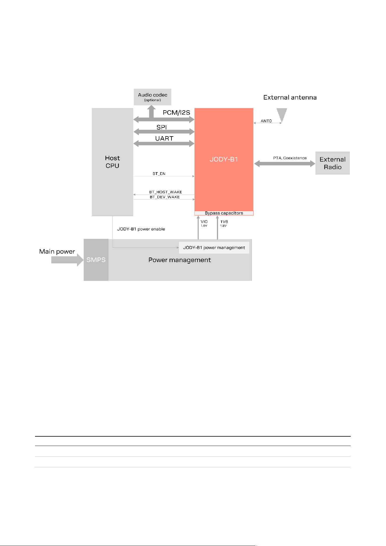
JODY-B1 shall be integrated into the application product together with a Host CPU.
Figure 1 shows a typical integration.
Figure 1: JODY-B1 integration in host system
• The UART interface is used for downloading the firmware and Bluetooth communication between
the host and the controller.
• Bluetooth enable and host and module wake up signals are available to control JODY-B1 to and
from host CPU.
• The module power is supplied through the 1V8 and VIO domain pins.
• For correct operation, it is important to correctly configure JODY-B1 with the settings and start-
up sequences described in this document and in the JODY-B1 data sheet [1]. This configuration
puts requirements for enabling the timing of power sources and the assertion of BT_EN.
• JODY-B1 includes a PCM/I2S interface that can be used to connect a codec for Bluetooth audio. If
the interface is not used, it can be omitted.
2.1 Power supply interface
JODY-B1 series System Integration Manual power supply pins 1V8 and VIO pins must be sourced by
a regulated DC power supply, such as an LDO or SMPS. The appropriate type for your design depends
on the main power source of the application.
Pin
Name
I/O
Description
Remarks
3
VIO
PWR
VIO supply
1.8 V
4
1V8
PWR
1.8 V supply
1.8 V
Table 1: Power supply pins
UBXDOC-465451970-3820 - R01 Module integration Page 7 of 44
C2-Restricted
The DC power supply can be taken from any of the following sources:
• Switched Mode Power Supply (SMPS)
• Low Drop Out (LDO) regulator
Module power up must strictly follow the defined power-up sequence. It is important to design the
power management to comply with the recommended power-up sequence.
The current consumed through the supply pins by JODY-B1 series System Integration Manual
modules can vary by several orders of magnitude depending on the operation mode and state. The
current consumption can change from high consumption, experienced during Bluetooth transmission
at maximum RF power level in connected-mode, to low current consumption during the low power idle-
mode when power saving is enabled. Regardless of the chosen DC power supply, it is crucial that it can
satisfy the high peak current consumed by the module. When designing the supply circuitry for the
module, a contingency of at least 20% over the stated peak current is recommended.
2.2 Antenna interfaces
JODY-B1 series System Integration Manual modules include an antenna pin to connect an external
antenna. Either integrated SMD or equivalent antennas mounted on application board or external
antenna connected through antenna connector and coaxial cable can be used.
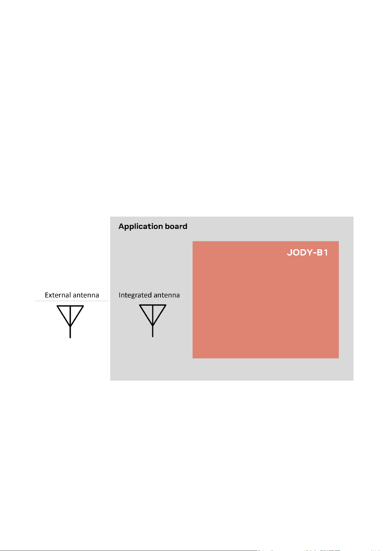
Figure 2: Antenna options
• External antenna: An external antenna of choice connected through a coaxial cable to an U.FL or
Reverse Polarity SMA connector placed on the application PCB and connected to the module
antenna pin.
• Integrated antenna: A permanent antenna included into the PCB application design. Ideally an
SMD antenna mounted on the application PCB or a Flexible PCB antenna attached to the
application product’s housing.

UBXDOC-465451970-3820 - R01 Module integration Page 8 of 44
C2-Restricted
2.2.1 RF pins and connectors
An RF pin is used to connect the Bluetooth antenna. Table 2 describes the function of the RF pins on
JODY-B1.
Pin
Name
I/O
Description
Remarks
24
ANT0
I/O, RF
Bluetooth
50
Table 2: RF pin allocation
⚠ For proper implementation of antennas in the application product, follow the RF interface options.
⚠ To implement a design compliant with the u-blox FCC certification Grant follow the instructions in
the Antenna Integration application note [10].
2.2.2 Approved antenna designs
JODY-B1 modules come with a pre-certified antenna design that can save time and expense during
the certification process. To leverage this benefit, customers are required to implement an antenna
layout that is fully compliant with the u-blox reference design outlined in future versions of this
document. Reference design source files are available from u-blox on request.
1
For Bluetooth operation, JODY-B1 modules have been tested and approved for use with the antennas
featured in the list of Pre-approved antennas .
To implement a design compliant with the u-blox FCC certification Grant follow the instructions in the
Antenna Integration application note [10].
2.2.3 Integrated antennas
JODY-B1 modules allow an SMD antenna to be mounted on the application board, connected with a
transmission line to the ANT0 pin.
For proper implementation of antennas in the application product, follow the RF interface options.
2.2.4 External antennas
External antennas can be used with JODY-B1 modules. The antennas are preferably connected to the
module through coaxial cable and a U.FL or RPSMA connector.
External antennas are particularly suited for application products housed in metal casings that
demand that the antennas are placed externally.
For proper implementation of antennas in the application product, follow the RF interface options.
⚠ To avoid invalidating the compliance and pre-certification of u-blox modules with the various
regulatory bodies, use only external antennas included the list of Pre-approved antennas. u-blox
modules may also be integrated with other antennas. In which case, OEM installers must certify
their own designs with the respective regulatory agencies.
1
Reference designs are only available after certification
UBXDOC-465451970-3820 - R01 Module integration Page 9 of 44
C2-Restricted
2.3 System function interfaces
2.3.1 Power-up sequence
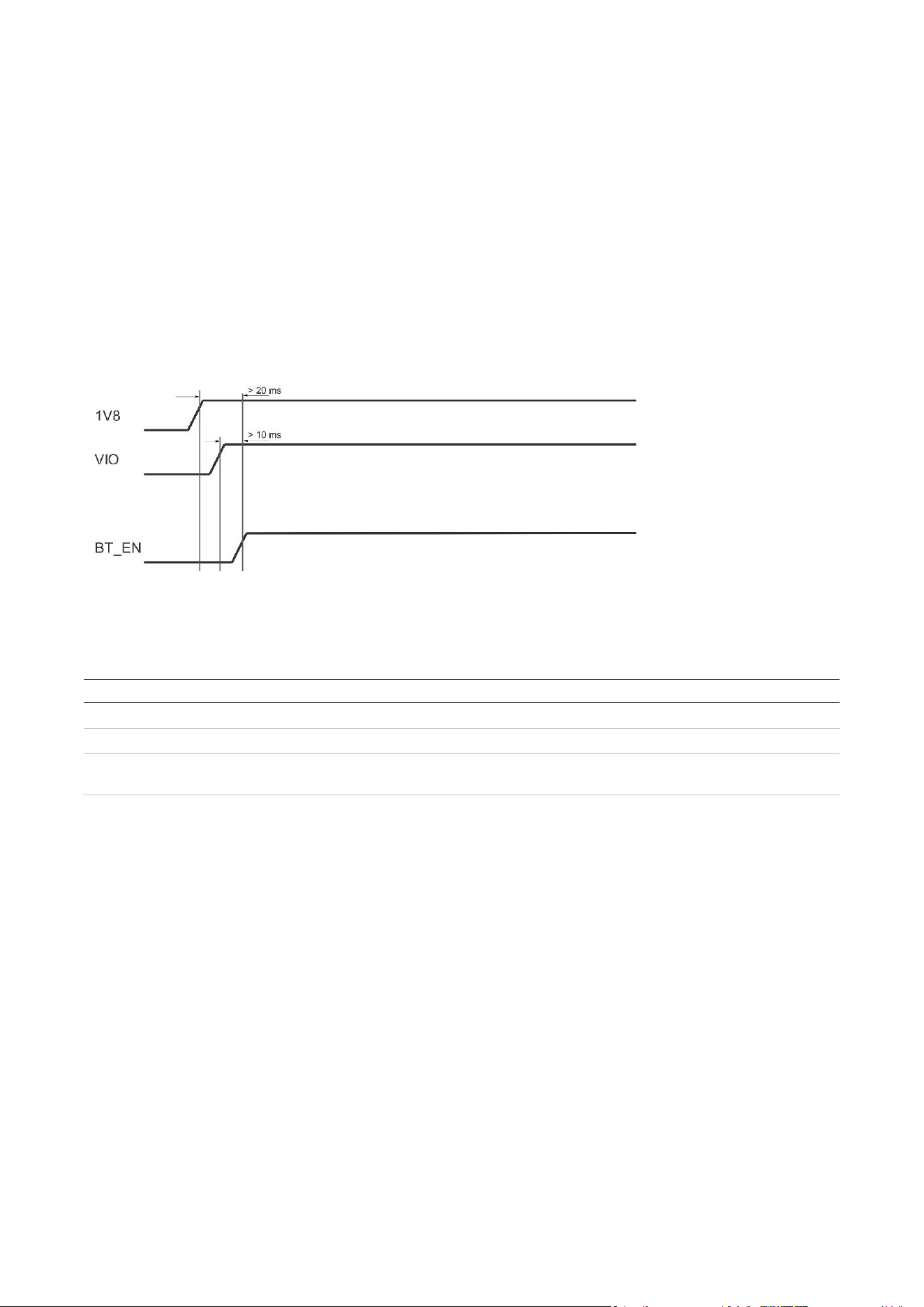
Figure 3 shows the recommended power-up sequence for JODY-B1. Startup is initiated by
simultaneously applying the 1V8 and VIO power supplies. After both supplies are stable, assert
BT_EN high after a minimum delay of 20 µs.
Alternatively, if the power supplies are applied individually:
• Wait at least 20 µs after 1V8 is applied.
• Wait at least 10 µs after VIO is applied.
• Then, set BT_EN high to complete the startup sequence.
Figure 3: Power-up sequence of JODY-B1 module
BT_EN shall be held low during start up and set high when the power is stable, or later when the
module must be turned on. BT_EN is powered by the VIO voltage domain.
Pin
Name
I/O
Description
Remarks
3
VIO
PWR
VIO supply (1.8 V)
4
1V8
PWR
1.8 V analog power supply
58
BT_EN
I
Bluetooth enable signal (active high) or reset,
external weak pull down may be required
Assert low for power down or
reset.
Table 3: Signals included in start-up sequence
☞ Power down mode can only be entered through BT_EN de-assertion by the host. For correct
reset, BT_EN must be set low for a minimum of 100 ms.
☞ All supply voltages must be monotonic.
2.3.2 Reset
Although external reset is not a prerequisite for correct operation, it can be asserted by the host
controller through BT_EN in the event of any abnormal module behavior.
JODY-B1 series modules are reset to a default operating state by any of the following events:
• Internal Power-On Reset is triggered when 1V8 and internal VCORE generated by an on-chip
DC/DC converter supplied from 1V8 is good (power good 90%).
• BT_EN de-assert: The device is reset when the BT_EN input pin is low.
☞ A firmware download to the module is required after each reset.

UBXDOC-465451970-3820 - R01 Module integration Page 10 of 44
C2-Restricted
2.3.3 Power-off sequence
JODY-B1 modules enter Power Down mode when BT_EN is set low. After de-assertion, 1V8 and VIO
supplies can be disabled. The module then enters Power Off mode.
2.3.4 Wake-up signals
JODY-B1 series System Integration Manual modules provide wake-up input and output signals that
handle the low-power modes. See also Power management.
The wake-up signals are used to exit JODY-B1 or host CPU from sleep modes. Wake-up signals are
powered by the VIO voltage domain. These signals are optional, out-of-band, wake-up pins that shall
be NC if not used.
Table 4 describes the various wake-up, input and output signals.
Pin
Name
I/O
Description
11
BT_DEV_WAKE
I
Host to Bluetooth Module wake-up signal (input)
12
BT_HOST _WAKE
O
Bluetooth Module to Host wake-up signal (output)
Table 4: Wake-up signal definitions
2.3.5 Power states
JODY-B1 series System Integration Manual modules have several operation states. The power states
and general guidelines for Bluetooth operations are defined in Table 5.
General status
Power state
Description
Power-down
Not Powered
1V8, and VIO supplies not present or below the operating range. The module is
switched off.
Power Down
Asserting BT_EN while 1V8, and VIO supplies are present powers down the module.
This represents the lowest leakage mode of operation with active voltage rails.
Register and memory states are not maintained in power-down mode. The module
is automatically reset after exiting power-down mode, which means that the
firmware must be downloaded again. If firmware is not downloaded, the device
must be kept in its power-down state to reduce the leakage.
Normal operation
Active
Enables TX/RX data connection with the system running at the specified power
consumption.
Deep sleep
Low-power state used in the sleep state of many power-save modes. Memory is
placed in low-power retention mode.
Table 5: Description of module power states
2.4 Host interfaces
2.4.1 High-speed UART interface
JODY-B1 series System Integration Manual modules use high-speed UART to connect to the host
CPU for firmware download and Bluetooth communication. The UART interface supports the HCI
UART transport layer as defined in the Bluetooth Core Specification, Version 5.0, Volume 4, Part A. In
addition to communication with the host, the HCI UART interface also supports Bluetooth software
(in-band) sleep control.
The main features of the UART interface include:
• Two pins for transmit and receive operations
• Two flow control pins (RTS/CTS)
• Supports standard baud rates and high throughput up to 3.2 Mbps. The default baud rate after
reset is 115.2 kbps.

UBXDOC-465451970-3820 - R01 Module integration Page 11 of 44
C2-Restricted
• Host baud rate tolerance is ±3%.
Table 6 describes the function of each of the UART signals.
Pin
Name
I/O
Description
Remarks
36
BT_UART_TX
O
UART serial output signal
Connect to Host RX
37
BT_UART_RX
I
UART serial input signal
Connect to Host TX
38
BT_UART_RTS
O
UART request-to-send output signal, active low
Connect to Host CTS
39
BT_UART_CTS
I
UART clear-to-send input signal, active low
Connect to Host RTS
Table 6: UART signal description
High-Speed UART signals are powered by the VIO voltage domain.

UBXDOC-465451970-3820 - R01 Module integration Page 12 of 44
C2-Restricted
2.4.2 SPI interface
The JODY-B1 supports a Serial Peripheral Interface (SPI). Table 7 describes the module pins for the
SPI interface.
Pin
Pin name
I/O
Description
61
BT_SPI_CLK
I
SPI clock input signal
64
BT_SPI_SS
I
SPI chip select signal
62
BT_SPI_MOSI
I
SPI data input signal
63
BT_SPI_MISO
O
SPI data output signal
Table 7: SPI interface description
2.4.3 PCM/I2S audio interface
JODY-B1 series System Integration Manual modules include a bi-directional, 4-wire, PCM digital audio
interface to connect an external digital audio device like an audio codec.
The PCM interface is configured to operate in central or peripheral mode. In each case, the PCM_IN
pin is the data receive terminal (input), and the PCM_OUT pin is the data transmit terminal (output).
The PCM_CLK and PCM_SYNC pins function as inputs or outputs, depending on whether the PCM
interface is configured as central or peripheral:
• When the JODY-B1 PCM interface is the central: PCM_CLK and PCM_SYNC are outputs from
the device to the PCM bus peripheral(s).
• When the JODY-B1 PCM interface is the peripheral: PCM_CLK and PCM_SYNC are inputs to
the device from the PCM bus central.
☞ PCM pins are shared with the I2S interface.
Table 8 describes the function of each of the PCM digital audio signals.
Pin
Name
I/O
Description
Remarks
16
PCM_CLK
I/O
PCM clock signal.
Alternate function: I2S clock
Output if central, input if
peripheral
15
PCM_SYNC
I/O
PCM frame sync signal.
Alternate function: I2S word select
Output if central, input if
peripheral
18
PCM_IN
I
PCM data input signal.
Alternate function: I2S data in
17
PCM_OUT
O
PCM data output signal.
Alternate function: I2S data out
Table 8: PCM digital audio signal descriptions
PCM/I2S signals are powered by the VIO voltage domain.

UBXDOC-465451970-3820 - R01 Module integration Page 13 of 44
C2-Restricted
2.5 External coexistence interface
The included PTA interface enables coexistence with an external radio. Table 9 describes the function
of each of the external coexistence signals.
Pin
Pin name
I/O
Description
90
PTA_PRI
I
PTA external radio priority signal
89
PTA_REQ
I
PTA request from the external radio
88
PTA_GNT
O
PTA external radio grant signal
Table 9: External coexistence interface description
2.6 JTAG
The module includes a JTAG test interface as shown in Table 10.
Pin
Pin name
I/O
Description
32
JTAG_TCK
I
JTAG test clock input signal
33
JTAG_TMS
I
JTAG controller select input signal
85
JTAG_TDO
O
JTAG test data output signal
86
JTAG_TDI
I
JTAG test data input signal
Table 10: JTAG interface description
2.7 Other remarks
2.7.1 Unused pins
JODY-B1 series modules have unconnected (NC) pins that are reserved for future use. These pins
must be left unconnected on the application board.

UBXDOC-465451970-3820 - R01 Design-in Page 14 of 44
C2-Restricted
3 Design-in
Follow the design guidelines in this chapter to optimize the integration of JODY-B1 series System
Integration Manual modules in the final application board.
3.1 Overview
Although all application circuits must be properly designed, and the following aspects of the
application design require special attention:
• Module antenna integration. ANT.
o Antennas and RF circuits affect the RF performance and certification compliance. It is
important to follow the design instructions given here to reach specified performance.
Further, to maintain compliance and subsequent certification of the application design, it is
important to observe the applicable parts of antenna schematic and layout described in
Antenna interfaces.
• Module power supply. Power and GND.
o Power supply circuits might affect the RF performance. It is important to select a suitable
device capable to source the adequate voltage and current. It is also important to implement
adequate power and ground planes in PCB stack-up and to implement bypass capacitors for
these supplies. See also Supply interfaces.
• High-speed interfaces, such as PCIe, SDIO, high-speed UART, and PCM.
o High-speed interfaces are a potential source of noise that can affect the regulatory compliance
of standards for radiated emissions. It is important to follow the schematic and layout design
recommendations described in General high-speed layout guidelines.
• System functions: Power Down, Reset and Configuration.
o Careful utilization of these pins in the application design is necessary to ensure that the
module operates as it should. Specifically, observe the state and voltage level is correctly
defined during module boot and operation. It is important to follow the pin design described in
the General high-speed layout guidelines.
• Other pins: specific signals.
o Careful utilization of these pins is necessary to ensure that the module operates as it should.
It is important to follow the schematic and design layout recommendations.
• NC pins must not be connected.
3.2 RF interface options
Short range modules provide several RF-interface options for connecting external antennas. Module
variants also provides internal or embedded antennas when using such module there are special
considerations to account when designing the host PCB:
• The ANT ports have a nominal characteristic impedance of 50 . For correct impedance matching,
these ports must be connected to the respective antenna through a 50 U.FL connector and coax
or a transmission line – depending on the type of module connector. Poor termination of ANT pins
will result in degraded performance of the module.

UBXDOC-465451970-3820 - R01 Design-in Page 15 of 44
C2-Restricted
⚠ According to FCC regulations, the transmission line from the module antenna pin to the physical
antenna (or antenna connector on the host PCB) is considered part of the approved antenna
design. Therefore, module integrators must use exactly the antenna reference design used in the
module FCC type approval or certify their own design.
For instructions on how to design circuits that comply with these requirements, see also Antenna
interfaces.
3.2.1 Antenna design
To optimize the radiated performance of the final product, the selection and placement of both the
module and antenna must be chosen with due regard to the mechanical structure and electrical
design of the product. To avoid later redesigns, it is important to decide the positioning of these
components at an early phase of the product design.
The compliance and subsequent certification of the RF design depends heavily on the radiating
performance of the antennas.
To ensure that the u-blox RF certification of modules is extended through to the application design,
carefully follow the guidelines outlined below.
• External antennas, including, linear monopole classes:
o Place the module and antenna in any convenient area on the board. External antennas do not
impose any restriction on where the module is placed on the PCB.
o Select antennas with an optimal radiating performance in the operating bands. The radiation
performance depends mainly on the antennas.
o Choose RF cables that offer minimum insertion loss. Unnecessary insertion loss is introduced
by low quality or long cables. Large insertion losses reduce radiation performance.
o Use a high-quality 50 coaxial connector for proper PCB-to-RF-cable transition.
• Integrated antennas, such as patch-like antennas:
o Internal integrated antennas impose some physical restrictions on the PCB design:
- Integrated antennas excite RF currents on its counterpoise, typically the PCB ground plane
of the device that becomes part of the antenna; its dimension defines the minimum
frequency that can be radiated. Therefore, the ground plane can be reduced to a minimum
size that should be similar to the quarter of the wavelength of the minimum frequency that
has to be radiated, given that the orientation of the ground plane related to the antenna
element must be considered.
- Find a numerical example to estimate the physical restrictions on a PCB, where:
Frequency = 2.4 GHz → Wavelength = 12.5 cm → Quarter wavelength = 3.5 cm in free space
or 1.5 cm on a FR4 substrate PCB.
• Choose antennas with optimal radiating performance in the operating bands. Radiation
performance depends on the complete product and antenna system design, including the
mechanical design and usage of the product. Table 11 summarizes the requirements for the
antenna RF interface.
• Make the RF isolation between the system antennas as high as possible, and the correlation
between the 3D radiation patterns of the two antennas as low as possible. In general, RF
separation of at least a quarter wavelength between the two antennas is required to achieve a
minimum isolation and low pattern correlation. If possible, increase the separation to maximize
the performance and fulfill the requirements described in Table 11.

UBXDOC-465451970-3820 - R01 Design-in Page 16 of 44
C2-Restricted
Item
Requirements
Remarks
Impedance
50 nominal characteristic
impedance
The impedance of the antenna RF connection must match
the 50 impedance of Antenna pins.
Frequency Range
2400 - 2500 MHz
Bluetooth.
Return Loss
S11 < -10 dB (VSWR < 2:1)
recommended
S11 < -6 dB (VSWR < 3:1) acceptable
The Return loss or the S11, as the VSWR, refers to the
amount of reflected power, measuring how well the primary
antenna RF connection matches the 50 characteristic
impedance of antenna pins.
The impedance of the antenna termination must match as
much as possible the 50 nominal impedance of antenna
pins over the operating frequency range, to maximize the
amount of power transferred to the antenna.
Efficiency
> -1.5 dB ( > 70% ) recommended
> -3.0 dB ( > 50% ) acceptable
Radiation efficiency is the ratio of the radiated power to the
power fed to the antenna input: the efficiency is a measure
of how well an antenna receives or transmits.
Maximum Gain
To comply with regulatory agencies radiation exposure
limits the maximum antenna gain must not exceed the
value specified in type approval documentation.
Table 11: Summary of antenna interface requirements
⚠ When operating dual antennas in the same 2.4 GHz band, sufficient isolation is critical for
attaining an optimal throughput performance in Wi-Fi/Bluetooth coexistence mode.
Select antennas that provide:
• Optimal return loss (or VSWR) over all the operating frequencies.
• Optimal efficiency figure over all the operating frequencies.
• An appropriate gain that does not exceed the regulatory limits specified in some regulatory
country authorities like the FCC in the United States.
A useful approach for the antenna micro-strip design is to place an U.FL connector close to the
embedded PCB or chip antenna. The U.FL connector only needs to be mounted on units used for
verification.
3.2.1.1 Integrated antenna design
If integrated antennas are used, the transmission line is terminated by the antennas themselves or
by the antenna together with the connected coaxial cable and U.FL plug.
Consider the following the guidelines when designing the antenna:
• The antenna design process should commence at the same time as the mechanical design of the
product. PCB mock-ups are useful in estimating overall efficiency and radiation path of the
intended design during early development stages.
• Use antennas designed by an antenna manufacturer that provide the best possible return loss (or
VSWR).
• Provide a ground plane large enough according to the related integrated antenna requirements.
The ground plane of the application PCB may be reduced to a minimum size that must be similar
to one quarter of wavelength of the minimum frequency that has to be radiated. The overall
antenna efficiency may benefit from larger ground planes.
• Proper placement of the antenna and its surroundings is also critical for antenna performance.
Avoid placing the antenna close to conductive or RF-absorbing parts, such as metal objects or
ferrite sheets, as these may absorb part of the radiated power, shift the resonant antenna
frequency of the antenna, or otherwise affect the antenna radiation pattern.
• Ensure that correct the installation and deployment of the antenna system, including PCB layout
and matching circuitry, is done correctly. In this regard, it is recommended that you strictly follow
the specific guidelines provided by the antenna manufacturer.
UBXDOC-465451970-3820 - R01 Design-in Page 17 of 44
C2-Restricted
• Further to the custom PCB and product restrictions, antennas may also require tuning/matching
to reach the target performance. It is recommended that you plan measurement and validation
activities with the antenna manufacturer before releasing the end-product to manufacturing.
• The receiver section may be affected by noise sources like hi-speed digital busses. Avoid placing
the antenna close to busses as DDR. Otherwise, consider taking specific countermeasures, like
metal shields or ferrite sheets, to reduce the interference.
• Be aware of interaction between co-located RF systems, like LTE sidebands on 2.4 GHz band.
Transmitted power may interact or disturb the performance of the module where specific LTE
filter is not present.
3.2.1.2 RF transmission line design
RF transmission lines, such as those that connect from ANT pins to their related antenna connectors
or antenna, must be designed with a characteristic impedance of 50 .
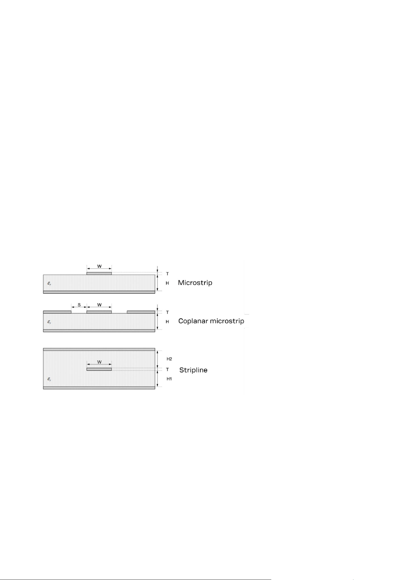
Figure 4 shows the design options and the most important parameters for designing a transmission
line on a PCB:
• Microstrip: track separated with dielectric material and coupled to a single ground plane.
• Coplanar microstrip: track separated with dielectric material and coupled to both the ground plane
and side conductor.
• Stripline: track separated by dielectric material and sandwiched between two parallel ground
planes.
The most common transmission line implementation is the coplanar microstrip, as shown in Figure 4.
Figure 4: Transmission line trace design
Follow these recommendations to design a 50 transmission line correctly:
• Designers must provide enough clearance from surrounding traces and ground in the same layer.
In general, the trace to ground clearance should be at least twice that of the trace width. The
transmission line should also be “guarded” by the ground plane area on each side.
• In the first iteration, calculate the characteristic impedance using tools provided by the layout
software. Ask the PCB manufacturer to provide the final values usually calculated using dedicated
software and production stack-ups. It is sometimes possible to request an impedance test coupon
on side of the panel to measure the real impedance of the traces.
• Although FR-4 dielectric material can result in high losses at high frequencies, it can still be an
appropriate choice for RF designs. In which case, aim to:
o Minimize RF trace lengths to reduce dielectric losses.
UBXDOC-465451970-3820 - R01 Design-in Page 18 of 44
C2-Restricted
o If traces longer than few centimeters are needed, use a coaxial connector and cable to reduce
losses.
o For good impedance control over the PCB manufacturing process, design the stack-up with
wide 50 traces with width of at least 200 µm.
o Contact the PCB manufacturer for specific tolerance of controlled impedance traces. As FR-4
material exhibits poor thickness stability it gives less control of impedance over the trace
width.
• For PCBs with components larger than 0402 and dielectric thickness below 200 µm, add a
keep-out, that is, some clearance (void area) on the ground reference layer below any pin on the RF
transmission lines. This helps to reduce the parasitic capacitance to ground.
• Route RF lines in 45 ° angle and avoid acute angles. The transmission lines width and spacing to
GND must be uniform and routed as smoothly as possible.
• Add GND stitching vias around transmission lines.
• Provide a sufficient number of vias on the adjacent metal layer. Include a solid metal connection
between the adjacent metal layer on the PCB stack-up to the main ground layer.
• To avoid crosstalk between RF traces and Hi-impedance or analog signals, route RF transmission
lines as far from noise sources (like switching supplies and digital lines) and any other sensitive
circuit.
• Avoid stubs on the transmission lines. Any component on the transmission line should be placed
with the connected pin located over the trace. Also avoid any unnecessary components on RF
traces.
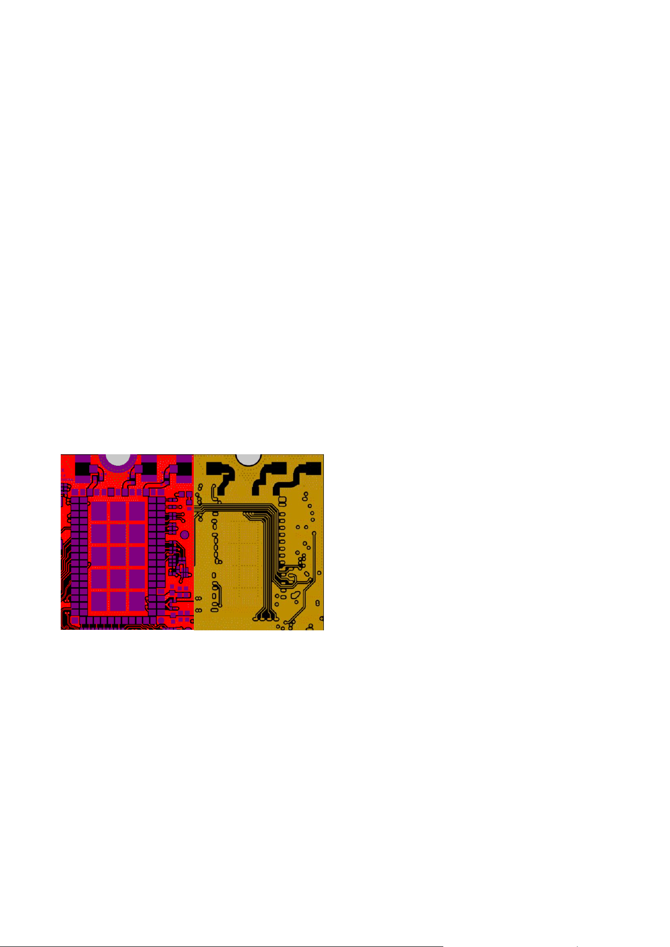
Figure 5 shows a trace and ground design example. The top layer, to the left, shows the transmission
line design connecting the RF pads to U.FL connectors. The purple rectangles are the top layer solder
pads.
Figure 5: RF trace and ground design example showing top layer and inner layer 1
Figure 5 shows typical artwork implementing a coplanar microstrip on a PCB. The trace includes
coplanar microstrip, impedance matching PI network, and U.FL. RF connectors. The ground clearance
on inner layers allow for a wider microstrip, which is less lossy than a narrow one. A wider trace also
has less impedance variation over PCB production batches due to the absolute tolerances in the PCB
etching process.
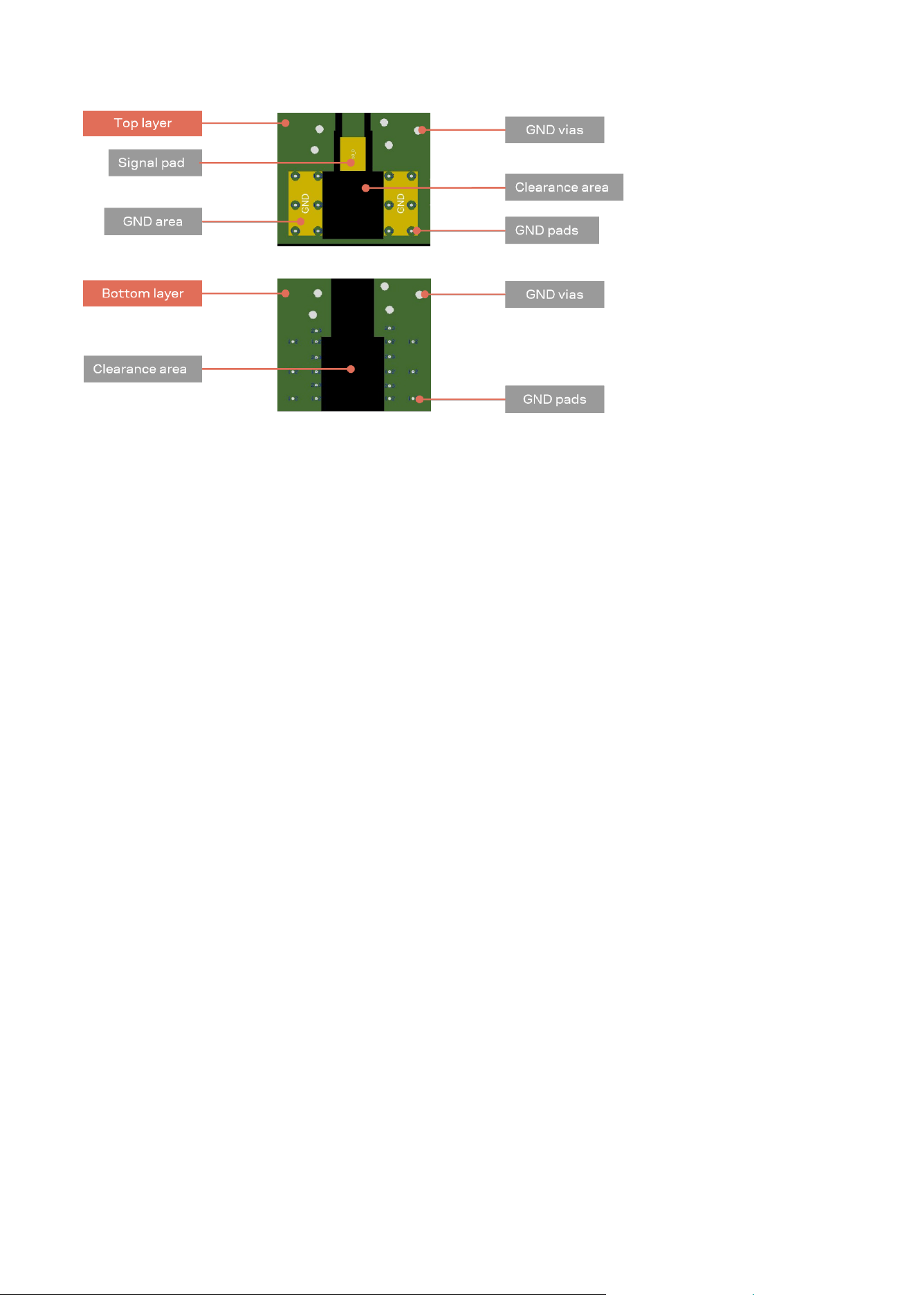
Figure 6 shows layout of pins for U.FL connector. Especially consider the GND clearance under the
signal pad.
UBXDOC-465451970-3820 - R01 Design-in Page 19 of 44
C2-Restricted
Figure 6: U.FL connector layout, top layer (top), and inner layer 1 (bottom)
3.3 Supply interfaces
3.3.1 Module supply design
Although the GND pins are internally connected, it is advisable to connect all available ground pins on
the application board to solid ground with a good (low impedance) connection to external ground. This
minimizes power loss, improves RF performance, and betters thermal performance.
Good connection of the module supply pins, supplied by a DC supply source, is required for accurate
RF performance.
Consider the following guidelines when developing the schematic:
• All power supply pins must be connected to an appropriate DC source.
• Any series component with an Equivalent Series Resistance (ESR) greater than a few mΩ should
be avoided. The only exception to this general rule is the use of ferrite beads for DC filtering. To
avoid possible instability in the DC supply, only use ferrite beads if needed.
• For high-frequency filtering, additional bypass capacitors in the range of 100 nF to 1 µF are
required on all supply pins. Offering low ESR/ESL resistance, a class II ceramic capacitor with an
X7R or X5R dielectric is well suited for this purpose. For +105 °C applications X6S dielectric
capacitors are recommended. Bypass capacitors of a smaller size can be chosen to minimize ESL
(Equivalent Series Inductance) in the manufacturing process. The capacitor should be placed as
close as possible to the module supply pin.
• In case of noise and immunity issues it is recommended to implement serial beads on especially
RF supply traces.
• To help filter current spikes from the RF section and avoid ground bounce, a minimum bulk
capacitance of 10 µF should be applied to the 1V8 rail (optionally on VIO) and placed close to the
module supply pins. Offering low ESR/ESL resistance, a class II ceramic capacitor with an X7R or
X5R dielectric is well suited for this purpose. Special care should be taken in the selection of
X5R/X7R dielectrics due to capacitance derating versus DC bias voltage.

UBXDOC-465451970-3820 - R01 Design-in Page 20 of 44
C2-Restricted
3.3.1.1 Guidelines for supply circuit design using an SMPS
When choosing between an SMPS or LDO to supply the modules, it is advisable to consider the
acceptable power and thermal dissipation of the application product.
A Switched Mode Power Supply (SMPS) is generally recommended for converting the main supply to
the module supply when the voltage difference is relatively high. In these circumstances, the use of
an SMPS dissipate less power and subsequently generates less power dissipation and heat than an
LDO. See also Regulated DC power supply.
By contrast, an LDO is generally simpler to use and does not generate the amount of noise an SMPS
might. See also Guidelines for supply circuit design using a Low Drop-Out (LDO) linear regulator.
To avoid degrading the module stability, RF performance, or violating spurious emission standards,
the characteristics of the SMPS should meet the following prerequisites:
• Power capability: The regulator, together with any additional filter in front of the module, must be
capable of providing a voltage within the specified operating range. It must also be capable of
delivering the specified peak current.
• Low output ripple: The peak-to-peak ripple voltage of the switching regulator must not exceed the
specified limits. This requirement is appliable to both the voltage ripple generated by the SMPS at
operating frequency and the high-frequency noise generated by power switching.
• PWM/PFM mode operation: It is advisable to select regulators that support a fixed Pulse Width
Modulation (PWM) mode. Pulse Frequency Modulation (PFM) mode typically exhibits higher ripple
and can affect RF performance. If power consumption is not a primary concern, PFM/PWM mode
transitions should be avoided in favor of fixed PWM operation to reduce the peak-to-peak noise on
voltage rails. Switching regulators with mixed PWM/PFM mode can be used provided that the
PFM/PWM modes and transition between modes complies with the requirements.
3.3.1.2 Guidelines for supply circuit design using a LDO linear regulator
The use of a linear regulator is appropriate when the difference between the available supply rail and
the module supply is relatively low. Linear regulators can also be considered for powering 1.8 V
domains – particularly those having low current requirements and those cascaded from an SMPS-
generated low voltage rail.
The characteristics of the Low Drop-Out (LDO) linear regulator used to power the voltage rails must
meet the following prerequisites:
• Power capabilities: The LDO linear regulator must be able to provide a voltage within the specified
operating range. It must also be capable of withstanding and delivering the maximum specified
peak current while in “connected mode”.
• Power dissipation: The power handling capability of the LDO linear regulator must be checked to
limit its junction temperature to the maximum rated operating range. The worst-case junction
temperature can be estimated as shown below:
𝑇
𝑗,𝑒𝑠𝑡
= (𝑉
𝑖𝑛
− 𝑉
𝑜𝑢𝑡
) ∗ 𝐼
𝑎𝑣𝑔
∗ 𝜃
𝑗𝑎
+ 𝑇
𝑎
Where: 𝜃
𝑗𝑎
is the junction-to-ambient thermal resistance of the LDO package
2
, 𝐼
𝑎𝑣𝑔
is the current
consumption of the given voltage rail in continuous TX/RX mode and 𝑇
𝑎
is the maximum operating
temperature of the end product inside the housing.
2
Thermal dissipation capability reported on datasheets is usually tested on a reference board with adequate copper area (see
also JESD51 [9]). Junction temperature on a typical PCB can be higher than the estimated value due to the limited space to
dissipate the heat. Thermal reliefs on pads also affect the capability of a device to dissipate heat.

UBXDOC-465451970-3820 - R01 Design-in Page 21 of 44
C2-Restricted
3.4 Data communication interfaces
3.4.1 High-speed UART interface
The high-speed UART interface for the JODY-B1 complies with the HCI UART Transport layer. The
module uses the settings shown in Table 12.
UART Settings
Baud rate default after reset
115200 baud
Data bits
8
Parity bit
No parity
Stop bit
1 stop bit
Flow Control
RTS/CTS
Table 12: HCI UART transport layer settings
RTS/CTS flow control is used to prevent temporary UART buffer overrun.
• If RTS is 0 (output, active low), the module is ready to receive, and the host is allowed to send.
• If CTS is 0 (input, active low), the host is ready to receive, and the module is allowed to send.
☞ The use of hardware flow control with RTS/CTS is mandatory.
Baud rate
9600
125000
720000
3000000
19200
230400
921600
3200000
38400
250000
1000000
57600
460800
1600000
115200
500000
2000000
Table 13: Possible baud rates for the UART interface
The baud rate accuracy of the UART interface is +1.5/-2.5% and the host baud rate tolerance is ±3%.
3.5 Other interfaces and notes
Most pins have internal keeper resistors; then leave un-used pins open. Otherwise, it is good practice
to follow below recommendation.
• Digital output signals might be left unconnected.
• Input signals without internal keeper resistors might be tied to GND or supply voltage through a
pull resistor. The same applies for analog inputs.
For JODY-B1 inputs without keepers applies to the I2S and SPI interfaces.
3.6 General high-speed layout guidelines
These guidelines describe best practices for the layout of all high-speed interfaces.
Designers should prioritize the layout of higher speed busses. Low frequency signals, other than those
with high-impedance traces, are generally not critical to the layout.
⚠ Low frequency signals with high-impedance traces (such as signals driven by weak pull resistors)
may be affected by crosstalk. For these high impedance traces, a supplementary isolation of 4*W
from other busses is recommended.

UBXDOC-465451970-3820 - R01 Design-in Page 22 of 44
C2-Restricted
3.6.1 General considerations for schematic design and PCB floor planning
• Verify which signal bus requires termination and add appropriate series resistor terminations to
the schematics.
• Carefully consider the placement of the module with respect to the antenna position and host
processor; minimize RF trace length first and then the communication interface length.
• SDIO bus routing must aim to keep layer-to-layer transition to a minimum.
• Verify the allowable stack-ups, and the controlled impedance dimensioning for antenna traces and
busses, with the PCB manufacturer.
• Verify that the power supply design and power sequence are compliant with the specifications
described in System function interfaces.
3.6.2 Component placement
• Accessory parts like bypass capacitors must be placed as close as possible to the module to
improve filtering capability. Prioritize placing the smallest capacitors close to module pins.
• Do not place components close to the antenna area. Follow the recommendations of the antenna
manufacturer to determine distance of the antenna in relation to other parts of the system.
Designers should also maximize the distance of the antenna to High-frequency busses, like DDRs
and related components. Alternatively, consider an optional metal shield to reduce interferences
that might otherwise be picked up by the antenna and subsequently reduce module sensitivity.
3.6.3 Layout and manufacturing
• Avoid stubs on high-speed signals. Test points or component pads should be placed over the PCB
trace.
• Verify the recommended maximum signal skew for differential pairs and length matching of
buses.
• Minimize the routing length; longer traces degrade signal performance. Ensure that maximum
allowable length for high-speed busses is not exceeded.
• Ensure to track your impedance matched traces. Consult early with your PCB manufacturer for
proper stack-up definition.
• RF, analog, and digital sections should have dedicated and clearly separated areas on the board.
• No digital routing is allowed in the GND reference plane area of RF traces (ANT pins and Antenna).
• Designers are strongly recommended to avoid digital routing beneath all layers of RF traces.
• Ground cuts or separation are not allowed below the module.
• As a first priority, minimize the length of the RF traces. Then, minimize bus length to reduce
potential EMI issues related to the radiation of digital busses.
• All traces (Including low speed or DC traces) must couple with a reference plane (GND or power).
High-speed busses should be referenced to the ground plane. If designers need to change the
ground reference, an adequate number of GND vias must be added in the area of transition. This
facilitates a low-impedance path between the two GND layers for the return current.
• Hi-speed busses are not allowed to change reference plane. If a change to the reference plane is
unavoidable, some capacitors should be added in the area to provide a low impedance return path
through the various reference planes.
• Trace routing should maintain a distance that is greater than 3*W from the edge of the ground
plane routing.
• Power planes should maintain a safe distance from the edge of the PCB. The distance must be
sufficient to route a ground ring around the PCB, and the ground ring must then be stitched to
other layers through vias.
• Route the power supply in low impedance power planes. If you choose to route the power supply
with traces, do not route loop structures.
UBXDOC-465451970-3820 - R01 Design-in Page 23 of 44
C2-Restricted
⚠ The heat dissipation during continuous transmission at maximum power can significantly raise
the temperature of application baseboards under modules. Avoid placing temperature sensitive
devices close to the module and provide these devices with sufficient grounding to transfer
generated heat to the PCB.
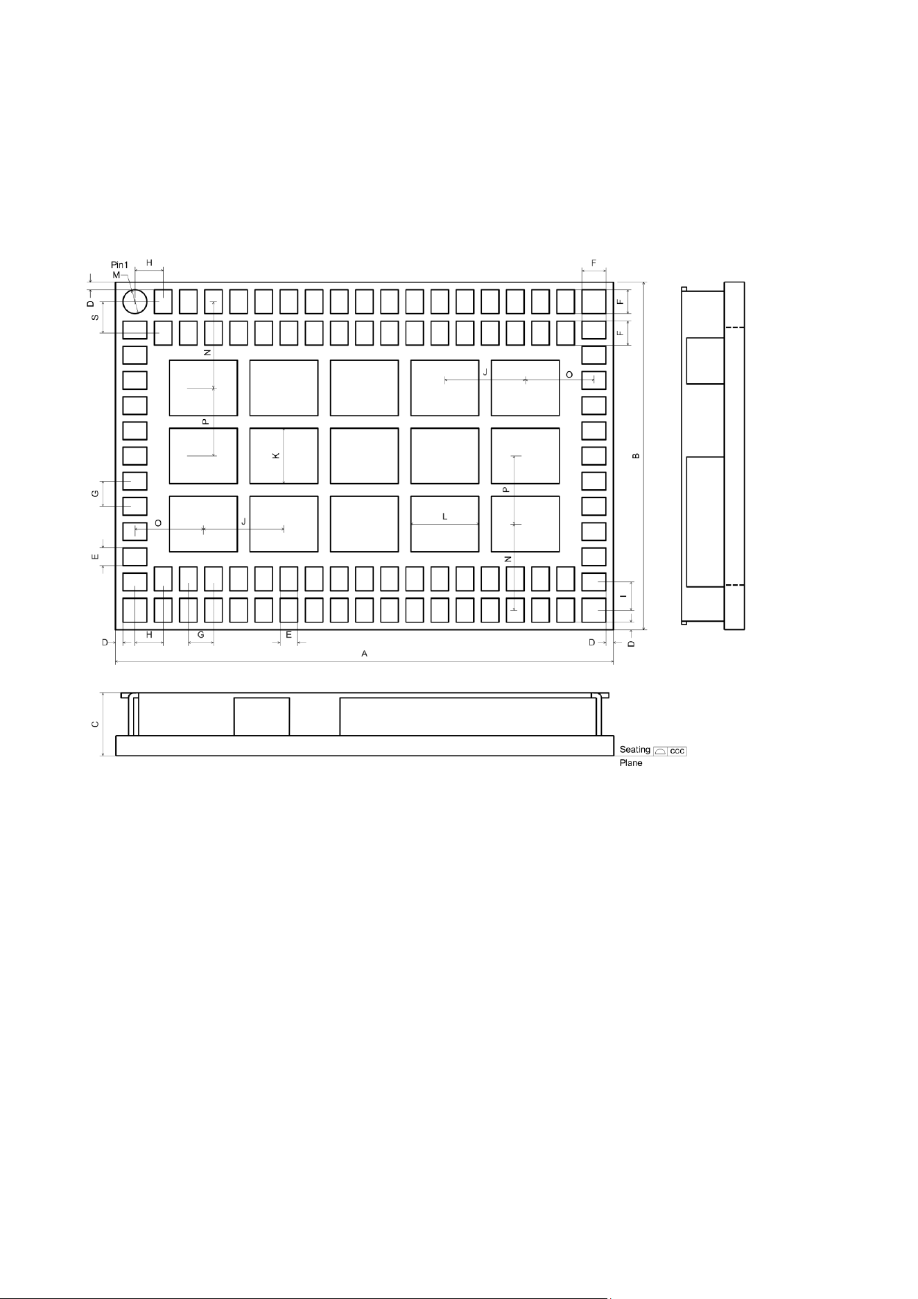
3.7 Module footprint and paste mask
Figure 7: Recommended footprint for JODY-B1, bottom view
Figure 7 shows the pin layout of JODY-B1 series System Integration Manual modules. Dimensions are
found in [1]. The proposed land pattern layout complements the pin layout of the module. Both Solder
Mask Defined (SMD) and Non Solder Mask Defined (NSMD) pins can be used with adherence to the
following considerations:
• All pins should be Non-Solder Mask Defined (NSMD)
• To help with the dissipation of the heat generated by the module, GND pads must have good
thermal bonding to PCB ground planes.
The suggested stencil layout for the JODY-B1 module is to follow the copper pad layout exactly as
described in Figure 7 for the outer pads, while the central pads should implement a special solder
paste pattern with the following characteristics:
• Solder paste area should be split in several smaller parts, typically four to nine depending on
copper pad area.
• Total solder paste area should cover about 50% to 60% of copper thermal pad area.
• Total solder paste area must not exceed 65% of copper thermal pad area.
Missing to consider solder paste optimization can lead to poor soldering quality in production.
A suggested stencil opening implementation is shown in Figure 8.

UBXDOC-465451970-3820 - R01 Design-in Page 24 of 44
C2-Restricted
Figure 8: Stencil opening example for inner thermal pads (dimensions in µm)
⚠ The exact mask geometries, distances and stencil thicknesses must be adapted to the specific
production process of the customer.
3.8 Thermal guidelines
JODY-B1 series System Integration Manual modules are designed to operate from -40 °C to +105 °C
at an ambient temperature inside the enclosure box. The board generates heat during high loads that
must be dissipated to sustain the lifetime of the components.
The improvement of thermal dissipation in the module decreases its internal temperature and
consequently increases the long-term reliability of device applications operating at high ambient
temperatures.
For best performance, layouts should adhere to the following guidelines:
• Vias specification for ground filling: 300/600𝜇𝑚, with no thermal reliefs allowed on vias.
• Ground via densities under the module: 50 𝑣𝑖𝑎𝑠/𝑐𝑚
2
; thermal vias can be placed in gaps between
the thermal pads of the module.
• Minimum layer count and copper thickness: 4 𝑙𝑎𝑦𝑒𝑟𝑠, 35 𝜇𝑚.
• Minimum board size: 55𝑥70 𝑚𝑚.
• To optimize the heat flow from the module, power planes and signal traces should not cross the
layers beneath the module.
These recommendations facilitate a design that is capable of achieving a thermal characterization
parameter of ψ
𝐽𝐵
= 𝑇𝐵𝐷 °𝐶/𝑊 for -40 °C to +105 °C where, 𝐽𝐵 refers to the junction between the
module and the bottom side of the main PCB characterization parameter.
Use the following hardware techniques to further improve thermal dissipation in the module and
optimize its performance in customer applications:
• Maximize the return loss of the antenna to reduce reflected RF power to the module.
• Improve the efficiency of any component that generates heat, including power supplies and
processor, by dissipating it evenly throughout the application device.
• Provide sufficient ventilation in the mechanical enclosure of the application.
• For continuous operation at high temperatures, particularly in high-power density applications or
smaller PCB sizes, include a heat sink on the bottom side of the main PCB. The heat sink is best
connected using electrically insulated / high thermal conductivity adhesive
3
.
3
Typically not required.

UBXDOC-465451970-3820 - R01 Design-in Page 25 of 44
C2-Restricted
3.9 ESD guidelines
In compliance with the following European regulations, designers must implement proper protection
measures against ESD events on any pin exposed to end users:
• ESD testing standard CENELEC EN 61000-4-2 [3]
• Radio equipment standard ETSI EN 301 489-1 [4]
The minimum requirements as per these European regulations are summarized in Table 14.
Application
Category
Immunity level
All exposed surfaces of the radio equipment and any ancillary equipment in
the end product.
Contact discharge
4 kV
Air discharge
8 kV
Table 14: Minimum ESD immunity requirements based on EN 61000-4-2
Compliance with the protection levels specified in EN 61000-4-2 [3] are fulfilled by including proper
ESD protection in parallel to any susceptible trace that is close to areas accessible to end users.
⚠ Special care should be taken with the ANT pins that must be protected by choosing an ESD
absorber or TVS diode with adequate parasitic capacitance. For 5 to 6 GHz operation, protection
with maximum internal capacitance of 0.1 pF is advised.
3.10 Design-in checklists
3.10.1 Schematic checklist
Check that the module pins have been properly numbered and designated in the schematic
(including thermal pins). See Pin definition in the JODY-B1 data sheet [1].
Power supply design complies with the voltage and power supply requirements described in the
module data sheet [1].
The Power-up sequence has been properly implemented.
Adequate bypassing has been included in front of each power pin. See Power-up sequence.
Each signal group is consistent with its own power rail supply or proper signal translation has been
provided. See Pin definition in the JODY-B1 data sheet [1].
Configuration pins are properly set at bootstrap. See Configuration pins.
Unused pins are properly terminated. See Unused pins and 3.5.
A pi-filter is provided in front of each antenna for final matching. High-speed UART interface.
Additional RF co-location filters have been considered in the design. See block diagrams in the
module data sheet [1].
3.10.2 Layout checklist
PCB stack-up and controlled impedance traces follow the recommendations given by the PCB
manufacturer. See RF transmission line design.
All pins are properly connected, and the footprint follows u-blox pin design recommendations. See
Module footprint and paste mask.
Proper clearance has been provided between the RF and digital sections of the design. See Layout
and manufacturing.
Proper isolation has been provided between antennas (RF co-location, diversity, or multi-antenna
design). See Layout and manufacturing.
Bypass capacitors have been placed close to the module. See Component placement.
Low impedance power path has been provided to the module. See Component placement.

UBXDOC-465451970-3820 - R01 Design-in Page 26 of 44
C2-Restricted
Controlled impedance traces have been properly implemented in the layout (both RF and digital)
and the recommendations provided by the PCB manufacturer have been followed. See RF
transmission line design and Component placement.
50 Ω RF traces and connectors follow the rules described in Antenna interfaces.
Antenna integration has been reviewed by the antenna manufacturer.
Proper grounding has been provided to the module for the low impedance return path and heat
sink. See Layout and manufacturing.
Reference plane skipping has been minimized for high frequency busses. See Layout and
manufacturing.
All traces and planes are routed inside the area defined by the main ground plane. See Layout and
manufacturing
u-blox has reviewed and approved the PCB
5
.
5
This is applicable only for end-products based on u-blox reference designs.

UBXDOC-465451970-3820 - R01 Software Page 27 of 44
C2-Restricted
4 Software
The chapter describes the available software options for JODY-B1 series System Integration Manual
modules, which are based on the Qualcomm QCA8695AU chipset. The drivers and firmware required
to operate JODY-B1 series System Integration Manual modules are developed by Qualcomm.
☞ For the latest JODY-B1 series System Integration Manual software deliverables, contact your
local support team.
UBXDOC-465451970-3820 - R01 Handling and soldering Page 28 of 44
C2-Restricted
5 Handling and soldering
⚠ JODY-B1 series modules are Electrostatic Sensitive Devices that demand the observance of
special handling precautions against static damage. Failure to observe these precautions can
result in severe damage to the product.
5.1 ESD handling precautions
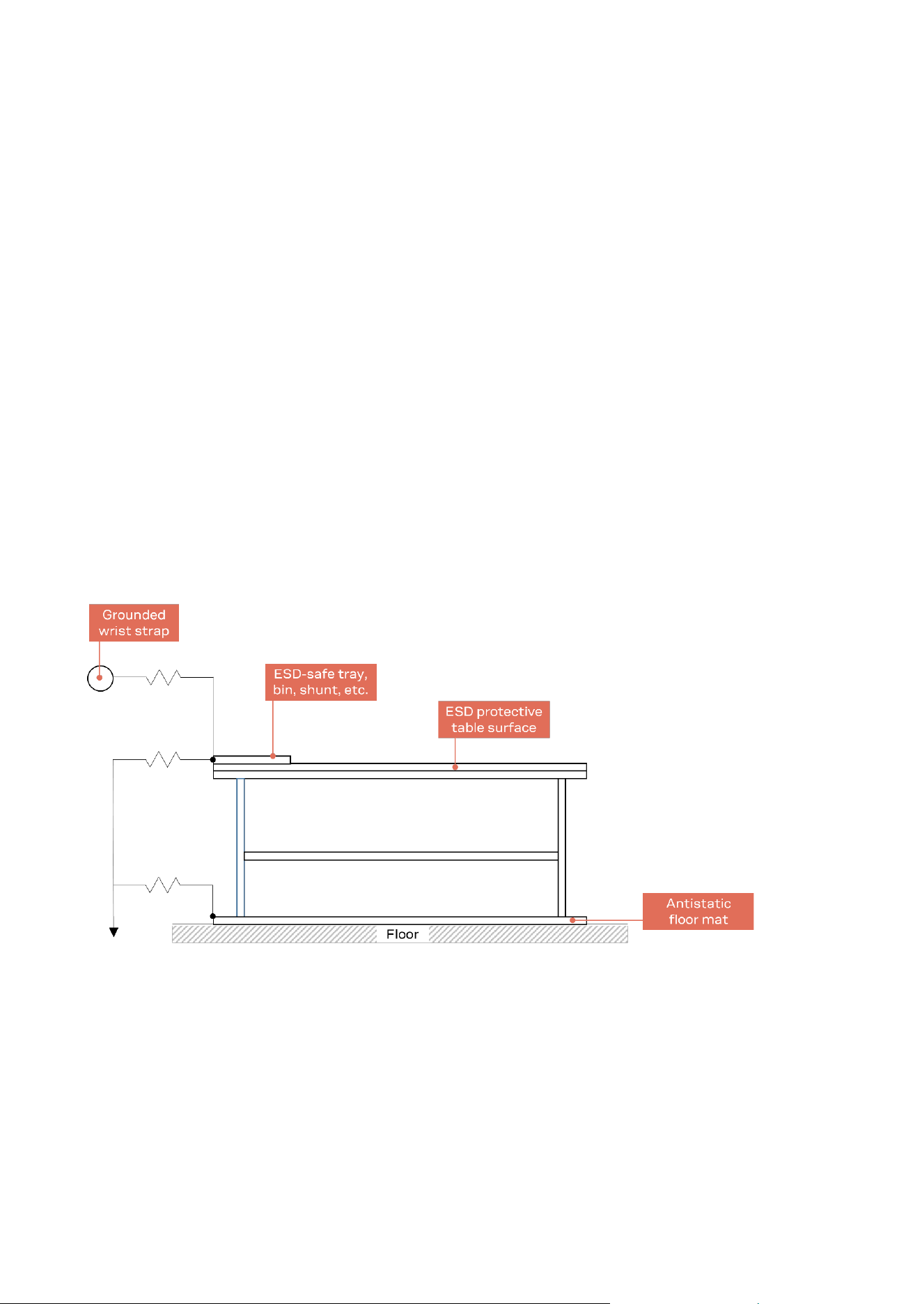
As the risk of electrostatic discharge in the RF transceivers and patch antennas of the module is of
particular concern, standard ESD safety practices are prerequisite. See also Figure 9.
Consider also:
• When connecting test equipment or any other electronics to the module (as a standalone or PCB-
mounted device), the first point of contact must always be to local GND.
• Before mounting an antenna patch, connect the device to ground.
• When handling the RF pin, do not touch any charged capacitors. Be especially careful when
handling materials like patch antennas (~10 pF), coaxial cables (~50-80 pF/m), soldering irons, or
any other materials that can develop charges.
• To prevent electrostatic discharge through the RF input, do not touch any exposed antenna area.
If there is any risk of the exposed antenna being touched in an unprotected ESD work area, be sure
to implement proper ESD protection measures in the design.
• When soldering RF connectors and patch antennas to the RF pin on the receiver, be sure to use an
ESD-safe soldering iron (tip).
Figure 9: Standard workstation setup for safe handling of ESD-sensitive devices
5.2 Packaging, shipping, storage, and moisture preconditioning
For information pertaining to reels, tapes, or trays, moisture sensitivity levels (MSL), storage,
shipment, and drying preconditioning, see the JODY-B1 series data sheet [1] and Packaging
information reference guide [2].
UBXDOC-465451970-3820 - R01 Handling and soldering Page 29 of 44
C2-Restricted
5.3 Reflow soldering process
☞ JODY-B1 is approved for two-time reflow processes.
JODY-B1 modules are surface mounted devices supplied on a multi-layer FR4-type PCB with gold-
plated connection pads. The modules are produced in a lead-free process using lead-free soldering
paste. The thickness of solder resist between the host PCB top side and the bottom side of the JODY-
B1 module must be considered for the soldering process.
JODY-B1 modules are compatible with industrial reflow profile for RoHS solders, and “no-clean”
soldering paste is strongly recommended.
The reflow profile used is dependent on the thermal mass of the entire populated PCB, the heat
transfer efficiency of the oven, and the type of solder paste that is used. The optimal soldering profile
must be trimmed for the specific process and PCB layout
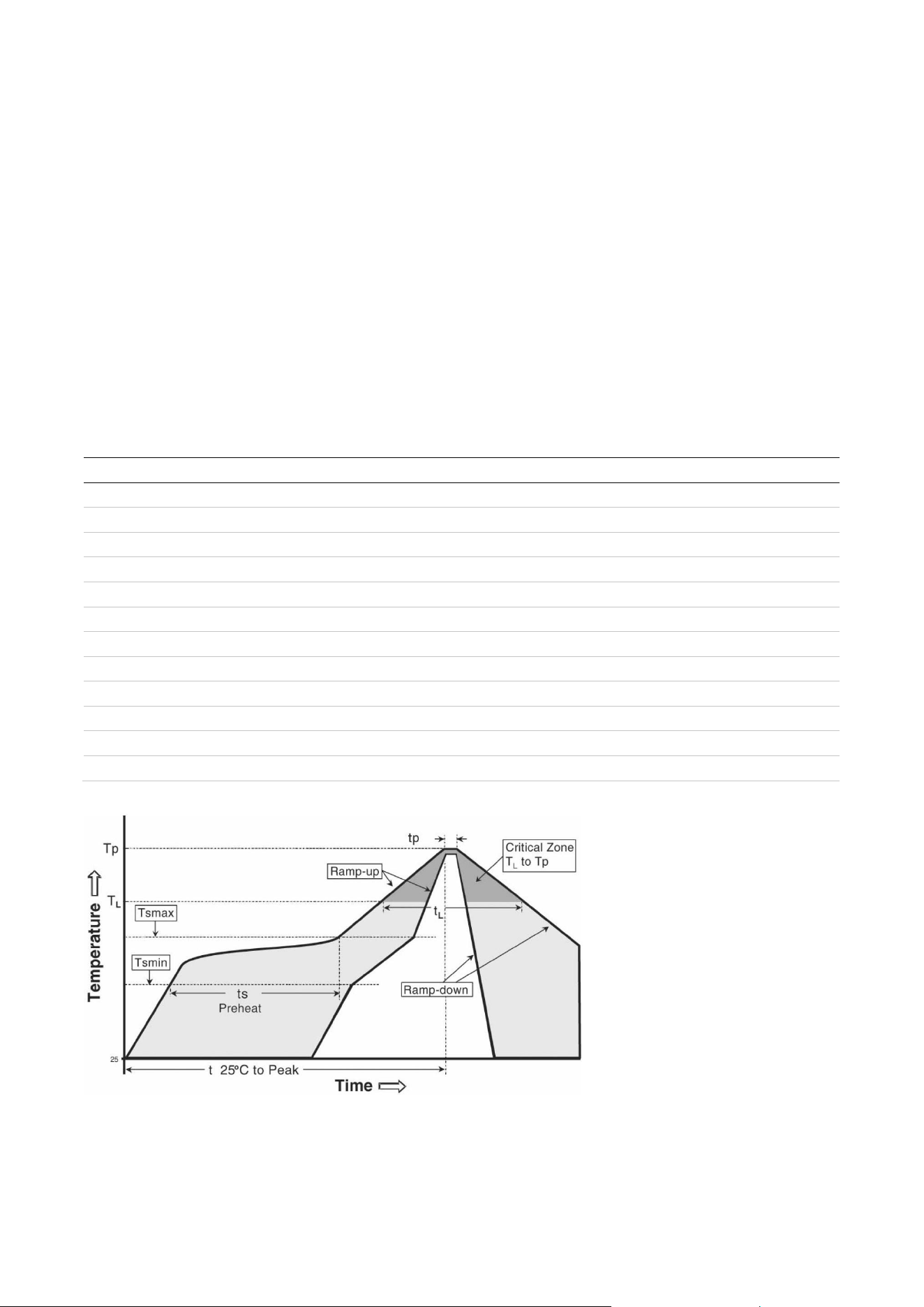
⚠ The target values shown in Table 15 and Figure 10 are given as general guidelines for a Pb-free
process only. For further information, see also the JEDEC J-STD-020E [6] standard.
Process parameter
Unit
Target
Pre-heat
Ramp up rate to T
SMIN
K/s
3
T
SMIN
°C
150
T
SMAX
°C
200
t
S
(from 25°C)
s
150
t
S
(Pre-heat)
s
110
Peak
T
L
°C
217
t
L
(time above T
L
)
s
90
T
P
°C
245-250
t
P
(time above T
P
-5°C)
s
30
Cooling
Ramp-down from T
L
(max)
K/s
6
General
T
to peak
s
300
Allowed reflow soldering cycles
-
2
Table 15: Recommended reflow profile
Figure 10: Reflow profile
☞ The lower value of T
P
and slower ramp down rate is preferred.

UBXDOC-465451970-3820 - R01 Handling and soldering Page 30 of 44
C2-Restricted
5.3.1 Cleaning
Cleaning the modules is not recommended. Residues underneath the modules cannot be easily
removed with a washing process.
• Cleaning with water will lead to capillary effects where water is absorbed in the gap between the
baseboard and the module. The combination of residues of soldering flux and encapsulated water
leads to short circuits or resistor-like interconnections between neighboring pins. Water will also
damage the sticker and the ink-jet printed text.
• Cleaning with alcohol or other organic solvents can result in soldering flux residues flooding into
the housing, areas that are not accessible for post-wash inspections. The solvent will also damage
the label and the ink-jet printed text.
• Ultrasonic cleaning will permanently damage the module and the crystal oscillators in particular.
For best results use a “no clean” soldering paste and circumvent the need for a cleaning stage after
the soldering process.
5.3.2 Other notes
• Boards with combined through-hole technology (THT) components and surface-mount
technology (SMT) devices may require wave soldering to solder the THT components. Only a single
wave-soldering process is allowed for boards populated with the modules. Miniature Wave
Selective Solder processes are preferred over traditional wave soldering processes.
• Hand-soldering is not recommended.
• Rework is not recommended.
• Conformal coating can affect the performance of the module, which means that it is important to
prevent the liquid from flowing into the module. The RF shields do not provide protection for the
module from coating liquids with low viscosity; therefore, care is required while applying the
coating. Conformal coating of the module will void the warranty.
• Grounding metal covers: Attempts to improve grounding by soldering ground cables, wick, or other
forms of metal strips directly onto the EMI covers is done so at the customer’s own risk and will
void the module warranty. The numerous ground pins on the module are adequate to provide
optimal immunity to interferences.
• The modules contain components which are sensitive to Ultrasonic Waves. Use of any Ultrasonic
Processes (cleaning, welding, etc.) may damage the module. The use of ultrasonic processes
together with the module will void the warranty.

UBXDOC-465451970-3820 - R01 Regulatory compliance Page 31 of 44
C2-Restricted
6 Regulatory compliance
6.1 General requirements
JODY-B1 series System Integration Manual modules are designed to comply with the regulatory
demands of Federal Communications Commission (FCC), Innovation, Science and Economic
Development Canada (ISED)
6
and the CE mark. This chapter contains instructions on the process
needed for an integrator when including the JODY-B1 module into an end-product.
• Any deviation from the process described may cause the JODY-B1 series System Integration
Manual module not to comply with the regulatory authorizations of the module and thus void the
user’s authority to operate the equipment.
• Any changes to hardware, hosts or co-location configuration may require new radiated emission
and SAR evaluation and/or testing.
• The regulatory compliance of JODY-B1 does not exempt the end-product from being evaluated
against applicable regulatory demands; for example, FCC Part 15B criteria for unintentional
radiators [8].
• The end-product manufacturer must follow all the engineering and operating guidelines as
specified by the grantee (u-blox).
• The JODY-B1 is for OEM integrators only.
• Only authorized antenna(s) may be used. Refer to JODY-B1 data sheet [1]
for the list of authorized
antennas. In the end-product, the JODY-B1 module must be installed in such a way that only
authorized antennas can be used.
• The end-product must use the specified antenna trace reference design, as described in the
JODY-B1 antenna reference design application note [14].
• Any notification to the end user about how to install or remove the integrated radio module is NOT
allowed.
⚠ If these conditions cannot be met or any of the operating instructions are violated, the u-blox
regulatory authorization will be considered invalid. Under these circumstances, the integrator is
responsible to re-evaluate the end-product including the JODY-B1 series System Integration
Manual module and obtain their own regulatory authorization, or u-blox may be able to support
updates of the u-blox regulatory authorization. See also Antenna requirements.
6.1 European Union regulatory compliance (pending)
JODY-B1 series modules comply with the essential requirements and other relevant provisions of
Radio Equipment Directive (RED) 2014/53/EU.
For information about the regulatory compliance of JODY-B1 series modules against requirements
and provisions in the European Union, see the JODY-B1 Declaration of Conformity [15].
6.1.1 CE End-product regulatory compliance
6.1.1.1 Safety standard
In order to fulfill the safety standard EN 60950-1 [7], the JODY-B1 module must be supplied with a
Class-2 Limited Power Source.
6
Formerly known as IC (Industry Canada).

UBXDOC-465451970-3820 - R01 Regulatory compliance Page 32 of 44
C2-Restricted
6.1.2 CE Equipment classes
In accordance with Article 1 of Commission Decision 2000/299/EC
7
, JODY-B1 is defined as either
Class-1 or Class-2 radio equipment, the end-product integrating JODY-B1 inherits the equipment
class of the module.
☞ For guidance on end product marking in according with RED, see http://ec.europa.eu/
⚠ The EIRP of the JODY-B1 module must not exceed the limits of the regulatory domain that the
module operates in. Depending on the host platform implementation and antenna gain,
integrators have to limit the maximum output power of the module through the host software. For
information about the corresponding maximum transmit power levels of Pre-approved antennas.
6.2 Great Britain regulatory compliance (pending)
For information about the regulatory compliance of JODY-B1 series modules against requirements
and provisions in Great Britain, see also the JODY-B1 UKCA Declaration of Conformity [16].
6.2.1 UK Conformity Assessed (UKCA)
☞ The United Kingdom is made up of the Great Britain (including England, Scotland, and Wales) and
the Northern Ireland. Northern Ireland continues to accept the CE marking. The following notice is
applicable to Great Britain only.
JODY-B1 series modules have been evaluated against the essential requirements of the Radio
Equipment Regulations 2017 (SI 2017 No. 1206, as amended by SI 2019 No. 696).
For guidance on end product marking in accordance with UKCA, see
https://www.gov.uk/guidance/using-the-ukca-marking.
6.3 United states/Canada End-product regulatory compliance
u-blox represents that the modular transmitter fulfills the FCC/ISED regulations when operating in
authorized modes on any host product given that the integrator follows the instructions as described
in this document. Accordingly, the host product manufacturer acknowledges that all host products
referring to the FCC ID or ISED certification number of the modular transmitter and placed on the
market by the host product manufacturer need to fulfil all of the requirements mentioned below. Non-
compliance with these requirements may result in revocation of the FCC approval and removal of the
host products from the market. These requirements correspond to questions featured in the FCC
guidance for software security requirements for U-NII devices, FCC OET KDB 594280 D02 [12].
⚠ The modular transmitter approval of JODY-B1, or any other radio module, does not exempt the
end product from being evaluated against applicable regulatory demands.
The evaluation of the end product shall be performed with the JODY-B1 module installed and
operating in a way that reflects the intended end product use case. The upper frequency
measurement range of the end product evaluation is the 5
th
harmonic of 2.4 GHz as described in KDB
996369 D04.
7
2000/299/EC: Commission Decision of 6 April 2000 establishing the initial classification of radio equipment and
telecommunications terminal equipment and associated identifiers.

UBXDOC-465451970-3820 - R01 Regulatory compliance Page 33 of 44
C2-Restricted
The following requirements apply to all products that integrate a radio module:
• Subpart B – UNINTENTIONAL RADIATORS
To verify that the composite device of host and module comply with the requirements of FCC part
15B, the integrator shall perform sufficient measurements using ANSI 63.4-2014.
• Subpart C – INTENTIONAL RADIATORS
It is required that the integrator carries out sufficient verification measurements using ANSI
63.10-2013 to validate that the fundamental and out of band emissions of the transmitter part of
the composite device complies with the requirements of FCC part 15C.
When the items listed above are fulfilled, the end product manufacturer can use the authorization
procedures as mentioned in Table 1 of 47 CFR Part 15.101, before marketing the end product. This
means the customer has to either market the end product under a Suppliers Declaration of
Conformity (SdoC) or to certify the product using an accredited test lab.
The description is a subset of the information found in applicable publications of FCC Office of
Engineering and Technology (OET) Knowledge Database (KDB). We recommend the integrator to read
the complete document of the referenced OET KDB’s.
• KDB 178919 D01 Permissive Change Policy
• KDB 447498 D01 General RF Exposure Guidance
• KDB 594280 D01 Configuration Control
• KDB 594280 D02 U-NII Device Security
• KDB 784748 D01 Labelling Part 15 18 Guidelines
• KDB 996369 D01 Module certification Guide
• KDB 996369 D02 Module Q&A
• KDB 996369 D04 Module Integration Guide
6.3.1 United States compliance statement (FCC)
JODY-B1 series modules have modular approval and comply with FCC 47 CFR Part 15C §15.247.
Operation is subject to the following two conditions:
• This device may not cause harmful interference, and
• This device must accept any interference received, including interference that may cause
undesired operation.
⚠ Any changes or modifications NOT explicitly APPROVED by u-blox could cause the JODY-B1 series
System Integration Manualmodule to cease to comply with FCC rules part 15 thus void the user's
authority to operate the equipment.
⚠ JODY-B1 series modular transmitter is only FCC authorized for the specific rule parts listed on the
FCC grant. The host product manufacturer is responsible for compliance to any other FCC rules
that apply to the host not covered by the modular transmitter grant of certification.
The internal / external antenna(s) used for this module must provide a separation distance of at least
20 cm from all persons and must not be co-located or operating in conjunction with any other antenna
or transmitter.
Table 16 shows the FCC IDs allocated to JODY-B1 series modules.
Model
FCC ID
JODY-B151-01A
XPYJODYB1
Table 16: FCC IDs for different variants of JODY-B1 series modules
For FCC end-product labeling requirements, see End product labeling requirements.

UBXDOC-465451970-3820 - R01 Regulatory compliance Page 34 of 44
C2-Restricted
6.3.2 Canada compliance statement (ISED)
JODY-B1 series modules are certified for use in accordance with the Canada Innovation, Science and
Economic Development Canada (ISED) Radio Standards Specification (RSS) RSS-247 Issue 4 and
RSS-Gen. Table 17 shows the ISED certification IDs allocated to the JODY-B1 series modules.
Model
ISED certification ID
JODY-B151-01A
8595A-JODYB1
Table 17: ISED IDs for different variants of JODY-B1 modules
Operation is subject to the following two conditions:
1. This device may not cause interference, and
2. This device must accept any interference, including interference that may cause undesired
operation of the device.
☞ Any notification to the end user of installation or removal instructions about the integrated radio
module is NOT allowed. Unauthorized modification could void authority to use this equipment.
This equipment complies with ISED RSS-102 radiation exposure limits set forth for an uncontrolled
environment. This equipment should be installed and operated with minimum distance 20 cm
between the radiator and your body.
This radio transmitter IC: 8595A-JODYB1 has been approved by ISED to operate with the antenna
types listed in Approved antennas with the maximum permissible gain indicated. Antenna types not
included in this list, having a gain greater than the maximum gain indicated for that type, are strictly
prohibited for use with this device.
Le présent appareil est conforme aux CNR d'ISED applicables aux appareils radio exempts de licence.
L'exploitation est autorisée aux deux conditions suivantes :
(1) l'appareil ne doit pas produire de brouillage, et
(2) l'utilisateur de l'appareil doit accepter tout brouillage radioélectrique subi, même si le brouillage est
susceptible d'en compromettre le fonctionnement.
Cet équipement est conforme aux limites d'exposition de rayonnement d'ISED RSS-102 déterminées
pour un environnement non contrôlé. Cet équipement devrait être installé et actionné avec la distance
minimum 20 cm entre le radiateur et votre corps.
Cet émetteur radio, IC: 8595A-JODYB1 été approuvé par ISED pour fonctionner avec les types
d’antenne énumérés dans la section Approved antennas avec le gain maximum autorisé et
l’impédance nécessaire pour chaque type d’antenne indiqué. Les types d’antenne ne figurant pas
dans cette liste et ayant un gain supérieur au gain maximum indiqué pour ce type-là sont strictement
interdits d’utilisation avec cet appareil.
The internal / external antenna(s) used for this module must provide a separation distance of at least
20 cm from all persons and must not be co-located or operating in conjunction with any other antenna
or transmitter.
For ISED end-product labeling requirements, see End product labeling requirements.
☞ The approval type for all JODY-B1 variants is a single modular approval. Due to ISED Modular
Approval Requirements (Source: RSP-100 Issue 10), any application which includes the module
must be approved by the module manufacturer (u-blox). The application manufacturer must
provide design data for the review procedure.

UBXDOC-465451970-3820 - R01 Regulatory compliance Page 35 of 44
C2-Restricted
6.3.3 Referring to the u-blox FCC/ISED certification ID
If the General requirements, United states/Canada End-product regulatory compliance and all
Antenna requirements are met, the u-blox modular FCC/ISED regulatory authorization is valid and the
end-product may refer to the u-blox FCC ID and ISED certification number. U-blox may be able to
support updates to the u-blox regulatory authorization by adding new antennas to the u-blox
authorization for example. See also Antenna requirements.
⚠ To use the u-blox FCC / ISED grant and refer to the u-blox FCC ID / ISED certification ID, the
integrator must confirm with u-blox that all requirements associated with the Configuration
control and software security of end-products are fulfilled.
6.3.4 Obtaining own FCC/ISED certification ID
Integrators who do not want to refer to the u-blox FCC/ISED certification ID, or who do not fulfil all
requirements to do so may instead obtain their own certification. With their own certification, the
integrator has full control of the grant to make changes.
Integrators who want to base their own certification on the u-blox certification can do so via a process
called “Change in ID” (FCC) / “Multiple listing” (ISED). With this, the integrator becomes the grantee
of a copy of the u-blox FCC/ISED certification. U-blox will support with an approval letter that shall be
filed as a Cover Letter exhibit with the application.
☞ For modules where the FCC ID / ISED certification ID is printed on the label, the integrator must
replace the module label with a new label containing the new FCC/ISED ID. For a description of
the labeling requirements, see also the JODY-B1 series System Integration Manual data sheet
[1].
⚠ It is the responsibility of the integrator to comply with any upcoming regulatory requirements.
6.3.5 Antenna requirements
In addition to the general requirement to use only authorized antennas, the u-blox grant also requires
a separation distance of at least 20 cm from the antenna(s) to all persons. The antenna(s) must not
be co-located with any other antenna or transmitter (simultaneous transmission) as well. If this
cannot be met, a Permissive Change as described below must be made to the grant.
☞ To support verification activities that may be required by certification laboratories, customers
applying for Class-II Permissive changes must implement the setup described in Software.
6.3.5.1 Separation distance
If the required separation distance of 20 cm cannot be fulfilled, a SAR evaluation must be performed.
This consists of additional calculations and/or measurements. The result must be added to the grant
file as a Class II Permissive Change.
6.3.5.2 Co-location (simultaneous transmission)
If the module is to be co-located with another transmitter, additional measurements for simultaneous
transmission are required. The results must be added to the grant file as a Class II Permissive Change.
6.3.5.3 Adding a new antenna for authorization
If the authorized antennas and/or antenna trace design cannot be used, the new antenna and/or
antenna trace designs must be added to the grant file. This is done by a Class I Permissive Change or
a Class II Permissive Change, depending on the specific antenna and antenna trace design.

UBXDOC-465451970-3820 - R01 Regulatory compliance Page 36 of 44
C2-Restricted
• Antennas of the same type and with less or same gain as those included in the list of Pre-approved
antennas can be added under a Class I Permissive Change.
• Antenna trace designs deviating from the u-blox reference design and new antenna types are
added under a Class II Permissive Change.
⚠ Integrators intending to refer to the u-blox FCC ID / ISED certification ID must contact their local
support team to discuss the Permissive Change Process. Class II Permissive Changes are subject
to NRE costs.
6.3.6 Configuration control and software security of end-products
☞ “Modular transmitter” hereafter refers to the JODY-B1 module with FCC ID: XPYJODYB1.
As the end-product must comply with the requirements addressed by the OET KDB 594280 [11], the
host product integrating the JODY-B1 must comply with the following requirements:
• Upon request from u-blox, the host product manufacturer will provide all of the necessary
information and documentation to demonstrate how the requirements listed below are met.
• The host product manufacturer will not modify the modular transmitter hardware.
• The configuration of the modular transmitter when installed into the host product must be within
the authorization of the modular transmitter at all times and cannot be changed to include
unauthorized modes of operation through accessible interfaces of the host product.
• The host product uses only authorized firmware images provided by u-blox and/or by the
manufacturer of the RF chipset used inside the modular transmitter.
• The modular transmitter must when installed into the host product have a regional setting that is
compliant with authorized US modes and the host product is protected from being modified by
third parties to configure unauthorized modes of operation for the modular transmitter, including
the country code.
• The host product into which the modular transmitter is installed does not provide any interface
for the installer to enter configuration parameters into the end product that exceeds those
authorized.
• The host product into which the modular transmitter is installed does not provide any interface to
third parties to upload any unauthorized firmware images into the modular transmitter and
prevents third parties from making unauthorized changes to all or parts of the modular
transmitter device driver software and configuration.
☞ OET KDB 594280 D01 [11] lists the topics that must be addressed to ensure that the end-
product specific host meets the Configuration Control requirements.
☞ OET KDB 594280 D02 [12] lists the topics that must be addressed to ensure that the end-
product specific host meets the Software Security Requirements for U-NII Devices.
6.3.7 End product labeling requirements
For an end-product using the JODY-B1 series modules, there must be a label containing, at least, the
following information:
This device contains
FCC ID: XPYJODYB1
IC: 8595A-JODYB1
(XYZ) represents the FCC “Grantee Code”, this code may consist of Arabic numerals, capital letters,
or other characters, the format for this code will be specified by the Commission’s Office of

UBXDOC-465451970-3820 - R01 Regulatory compliance Page 37 of 44
C2-Restricted
Engineering and Technology
10
. (CN) is the Company Number registered at ISED. (UPN) is the Unique
Product Number decided by the grant owner.
The label must be affixed on an exterior surface of the end product such that it will be visible upon
inspection in compliance with the modular labeling requirements of OET KDB 784748. The host user
manual must also contain clear instructions on how end users can find and/or access the FCC ID of
the end product.
The label on the JODY-B1 module containing the original FCC ID acquired by u-blox can be replaced
with a new label stating the end-product’s FCC/ISED ID in compliance with the modular labeling
requirements of OET KDB 784748.
FCC end product labeling
The outside of final products containing the JODY-B1 module must display in a user accessible area
a label referring to the enclosed module. This exterior label can use wording such as the following:
“Contains Transmitter Module FCC ID: XPYJODYB1” or “Contains FCC ID: XPYJODYB1”.
In accordance with 47 CFR § 15.19, the end product shall bear the following statement in a
conspicuous location on the device:
This device complies with Part 15 of the FCC Rules. Operation is subject to the following two conditions:
This device may not cause harmful interference, and
This device must accept any interference received, including interference that may cause undesired operation.
The following statement must be included in the end-user manual or guide:
ISED end product labeling
The ISED certification label of a module shall be clearly visible at all times when installed in the host
device; otherwise, the host device must be labeled to display the ISED certification number for the
module, preceded by the words “Contains transmitter module”, or the word “Contains”, or similar
wording expressing the same meaning, as follows: “Contains transmitter module IC: 8595A-
JODYB1”.
10
47 CFR 2.926
Changes or modifications to this unit not expressly approved by the party responsible for
compliance could void the user’s authority to operate the equipment.
This equipment has been tested and found to comply with the limits for a Class B digital device,
pursuant to part 15 of the FCC Rules. These limits are designed to provide reasonable protection
against harmful interference in a residential installation. This equipment generates uses and can
radiate radio frequency energy and, if not installed and used in accordance with the instructions,
may cause harmful interference to radio communications. However, there is no guarantee that
interference will not occur in a particular installation. If this equipment does cause harmful
interference to radio or television reception, which can be determined by turning the equipment
off and on, the user is encouraged to try to correct the interference by one or more of the
following measures:
Reorient or relocate the receiving antenna.
Increase the separation between the equipment and receiver.
Connect the equipment into an outlet on a circuit different from that to which the receiver is
connected.
Consult the dealer or an experienced radio/TV technician for help.

UBXDOC-465451970-3820 - R01 Regulatory compliance Page 38 of 44
C2-Restricted
L’étiquette d’homologation d’ISED d’un module donné doit être posée sur l’appareil hôte à un endroit
bien en vue en tout temps. En l’absence d’étiquette, l’appareil hôte doit porter une étiquette sur
laquelle figure le numéro d’homologation du module d’ISED, précédé des mots « Contient un module
d’émission », ou du mot « Contient », ou d’une formulation similaire allant dans le même sens et qui va
comme suit : « Contient le module d’émission IC: 8595A-JODY-B1.
The end product shall bear the following statement in both English and French in a conspicuous
location on the device:
Operation is subject to the following two conditions:
This device may not cause interference, and
This device must accept any interference, including interference that may cause undesired operation of the device.
Son utilisation est soumise aux deux conditions suivantes :
Cet appareil ne doit pas causer d’interférences et
il doit accepter toutes interférences reçues, y compris celles susceptibles d’avoir des effets indésirables sur son
fonctionnement.
When the device is so small or for such use that it is not practicable to place the statements above on
it, the information shall be placed in a prominent location in the instruction manual or pamphlet
supplied to the user or, alternatively, shall be placed on the container in which the device is marketed.
However, the FCC/ISED ID label must be displayed on the device as described above.
In case, where the final product will be installed in locations where the end-consumer is unable to see
the FCC/ISED ID and/or this statement, the FCC/ISED ID and the statement shall also be included in
the end-product manual.
6.4 Pre-approved antennas
For the specifications that must be fulfilled in the end product that uses radio type approval of the
JODY-B1 module, see the JODY-B1 antenna reference design application note [14].
The JODY-B1 antenna reference design application note provides PCB layout details and electrical
specifications.
The JODY-B1 modules has been tested and approved for use with the antennas described in Table
18.
Manufacturer
Part number
Antenna type
Peak gain [dBi]
Validated regulatory domain
Linx
Technologies
ANT-DB1-RAF-RPS
Dipole antenna
4.1
US/Canada (FCC/ISED)
EU/Great Britain (RED/UKCA)
Chang Hong
DA-2458-02-SMR
Dipole antenna
2.85
US/Canada (FCC/ISED)
EU/Great Britain (RED/UKCA)
TE
Connectivity
001-0012
Dipole antenna
2.0
US/Canada (FCC/ISED)
EU/Great Britain (RED/UKCA)
Taoglas
GW.59.3153
Dipole antenna
3.8
US/Canada (FCC/ISED)
EU/Great Britain (RED/UKCA)
Laird
MAF94051
Dipole antenna
2.1
US/Canada (FCC/ISED)
EU/Great Britain (RED/UKCA)
Molex
1461530050
PCB patch
3.2
US/Canada (FCC/ISED)
EU/Great Britain (RED/UKCA)
Molex
2042810100
PCB patch
2.0
US/Canada (FCC/ISED)
EU/Great Britain (RED/UKCA)
Unictron
H2B1PD1A1C385L
PCB patch
2.7
US/Canada (FCC/ISED)
EU/Great Britain (RED/UKCA)
Table 18: List of approved antennas

UBXDOC-465451970-3820 - R01 Regulatory compliance Page 39 of 44
C2-Restricted

UBXDOC-465451970-3820 - R01 Product testing Page 40 of 44
C2-Restricted
7 Product testing
7.1 u-blox in-line production testing
As part of our focus on high quality products, u-blox maintain stringent quality controls throughout
the production process. This means that all units in our manufacturing facilities are fully tested and
that any identified defects are carefully analyzed to improve future production quality.
The Automatic test equipment (ATE) deployed in u-blox production lines logs all production and
measurement data – from which a detailed test report for each unit can be generated. Figure 11
shows the ATE typically used during u-blox production.
u-blox in-line production testing includes:
• Digital self-tests (firmware download, MAC address programming)
• Measurement of voltages and currents
• Functional tests (host interface communication)
• Digital I/O tests
• Measurement and calibration of RF characteristics in all supported bands, including RSSI
calibration, frequency tuning of reference clock, calibration of transmitter power levels, etc.
• Verification of Wi-Fi and Bluetooth RF characteristics after calibration, like modulation accuracy,
power levels, and spectrum, are checked to ensure that all characteristics are within tolerance
when the calibration parameters are applied.
Figure 11: Automatic test equipment for module test

UBXDOC-465451970-3820 - R01 Product testing Page 41 of 44
C2-Restricted
7.2 OEM manufacturer production test
As all u-blox products undergo thorough in-series production testing prior to delivery, OEM
manufacturers do not need to repeat any firmware tests or measurements that might otherwise be
necessary to confirm RF performance. Testing over analog and digital interfaces is also unnecessary
during an OEM production test.
OEM manufacturer testing should ideally focus on:
• Module assembly on the device; it should be verified that:
o Soldering and handling process did not damage the module components
o All module pins are well soldered on the application board
o There are no short circuits between pins
• Component assembly on the device; it should be verified that:
o Communication with host controller can be established
o The interfaces between module and device are working
o Overall RF performance test of the device including antenna
In addition to this testing, OEMs can also perform other dedicated tests to check the device. For
example, the measurement of module current consumption in a specified operating state can identify
a short circuit if the test result deviates that from that taken against a “Golden Device”.
The standard operational module firmware and test software on the host can be used to perform
functional tests (communication with the host controller, check interfaces) and perform basic RF
performance testing. Special manufacturing firmware can also be used to perform more advanced RF
performance tests.

UBXDOC-465451970-3820 - R01 Appendix Page 42 of 44
C2-Restricted
Appendix
A Glossary
Abbreviation
Definition
AEC
Automotive Electronics Council
AP
Access Point
API
Application Programming Interface
ATE
Automatic Test Equipment
BT
Bluetooth
CDM
Charged Device Model
CE
European Conformity
CTS
Clear to Send
DC
Direct Current
DDR
Double Data Rate
DFS
Dynamic Frequency Selection
DHCP
Dynamic Host Configuration Interface
EDR
Enhanced Data Rate
EEPROM
Electrically Erasable Programmable Read-Only Memory
EIRP
Equivalent Isotropic Radiated Power
EMI
Electromagnetic Interference
ESD
Electro Static Discharge
ESL
Equivalent Series Inductance
ESR
Equivalent Series Resistance
FCC
Federal Communications Commission
GND
Ground
GPIO
General Purpose Input/Output
HBM
Human Body Model
HS
High-Speed
HCI
Host Controller Interface
ISED
Innovation, Science and Economic Development Canada
I2C
Inter-Integrated Circuit
KDB
Knowledge Database
LAN
Local Area Network
LDO
Low Drop Out
LED
Light-Emitting Diode
LPO
Low Power Oscillator
LTE
Long Term Evolution
MAC
Medium Access Control
MMC
Multi Media Card
MWS
Mobile Wireless Standards
NRE
Non-recurring engineering
NSMD
Non Solder Mask Defined
OEM
Original equipment manufacturer
OET
Office of Engineering and Technology
OS
Operating System

UBXDOC-465451970-3820 - R01 Appendix Page 43 of 44
C2-Restricted
Abbreviation
Definition
PCB
Printed Circuit Board
PCI
Peripheral Component Interconnect
PCIe
PCI Express
PCM
Pulse-code modulation
PHY
Physical layer (of the OSI model)
PMU
Power Management Unit
RF
Radio Frequency
RSDB
Real Simultaneous Dual Band
RST
Request to Send
SDIO
Secure Digital Input Output
SMD
Solder Mask Defined
SMPS
Switching Mode Power Supply
SMT
Surface-Mount Technology
SSID
Service Set Identifier
STA
Station
TBD
To be Decided
THT
Through-Hole Technology
UART
Universal Asynchronous Receiver-Transmitter
VCC
IC power-supply pin
VIO
Input offset voltage
VSDB
Virtual Simultaneous Dual Band
VSWR
Voltage Standing Wave Ratio
WFD
Wi-Fi Direct
WLAN
Wireless local area network
WPA
Wi-Fi Protected Access
Table 19: Explanation of the abbreviations and terms used

UBXDOC-465451970-3820 - R01 Related documents Page 44 of 44
C2-Restricted
Related documents
[1] JODY-B1 series data sheet, UBXDOC-1953704497-141
[2] Packaging information reference, UBX-14001652
[3] IEC EN 61000-4-2 – Electromagnetic compatibility (EMC) – Part 4-2: Testing and
measurement techniques – Electrostatic discharge immunity test
[4] ETSI EN 301 489-1 – Electromagnetic compatibility and Radio spectrum Matters (ERM);
ElectroMagnetic Compatibility (EMC) standard for radio equipment and services; Part 1:
Common technical requirements
[5] IEC61340-5-1 – Protection of electronic devices from electrostatic phenomena – General
requirements
[6] JEDEC J-STD-020E – Moisture/Reflow Sensitivity Classification for Nonhermetic Surface
Mount Devices
[7] ETSI EN 60950-1:2006 – Information technology equipment – Safety – Part 1: General
requirements
[8] FCC Regulatory Information, Title 47 – Telecommunication
[9] JESD51 – Overview of methodology for thermal testing of single semiconductor devices
[10] Antenna Integration application note, UBX-TBD
[11] FCC guidance 594280 D01 Configuration Control v02 r01,
[12] FCC guidance 594280 D02 U-NII Device Security v01r03
[13] JODY-B1 product summary, UBX-TBD
[14] JODY-B1 antenna reference design application note, UBX-TBD
[15] JODY-B1 RED Declaration of Conformity, UBX-TBD
[16] JODY-B1 UKCA Declaration of Conformity, UBX-TBD
☞ For product change notifications and regular updates of u-blox documentation, register on our
website, www.u-blox.com.
Revision history
Revision
Date
Name
Comments
R01
16-Jun-2025
lber
Initial release
Contact
u-blox AG
Address: Zürcherstrasse 68
8800 Thalwil
Switzerland
For further support and contact information, visit us at www.u-blox.com/support.