
1
FORM NO.: FR2-015_ A Responsible Department:WBU Expiry Date: Forever
The information contained herein is the exclusive property of AzureWave and shall not be distributed, reproduced, or
disclosed in whole or in part without prior written permission of AzureWave.
AW-CM689
IEEE 802.11 n Wi-Fi with ac friendly
+ Bluetooth 5.4 Combo LGA Module
Datasheet
Rev. B
DF
(For Standard)

2
FORM NO.: FR2-015_ A Responsible Department:WBU Expiry Date: Forever
The information contained herein is the exclusive property of AzureWave and shall not be distributed, reproduced, or
disclosed in whole or in part without prior written permission of AzureWave.
Features
WLAN
Full IEEE 802.11a/b/g/n compatibility with
enhanced performance:
802.11ac friendly, MCS8 (256-QAM) for 20
MHz channels in 5 GHz band.
Single spatial stream with PHY data rates of
up to 72.2 Mbps with 802.11n (MCS7) and 78
Mbps with 802.11ac (MCS8).
20 MHz channels with optional SGI support
for MCS0-MCS7.
IEEE 802.11ac explicit beamformer support.
TX and RX low-density parity check (LDPC)
support for improved range and power
efficiency.
Receive space-time block coding (STBC)
On-chip power amplifier/low-noise amplifier
for both bands.
Bluetooth
All optional Bluetooth 5.4 features supported.
Bluetooth Class 1 or Class 2 transmitter
operation.
Supports BDR (1Mbps), EDR (2/3Mbps), BLE
(1/2Mbps).
Host controller interface (HCI) using a high-
speed UART interface.
PCM for audio data.
Bluetooth 5.4 compliant with 2 Mbps GFSK
data rate for BLE.
3
FORM NO.: FR2-015_ A Responsible Department:WBU Expiry Date: Forever
The information contained herein is the exclusive property of AzureWave and shall not be distributed, reproduced, or
disclosed in whole or in part without prior written permission of AzureWave.
Revision History
Document NO: R2-2689-DST-01
Version
Revision Date
DCN NO.
Description
Initials
Approved
A
2025/02/06
DCN033402
Initial Version
Ashley Lin
N.C Chen
B
2025/05/29
DCN034527
Specifications Table
update
Barry Tsai
N.C Chen

4
FORM NO.: FR2-015_ A Responsible Department:WBU Expiry Date: Forever
The information contained herein is the exclusive property of AzureWave and shall not be distributed, reproduced, or
disclosed in whole or in part without prior written permission of AzureWave.
Table of Contents
Revision History .............................................................................................................................. 3
1. Introduction ................................................................................................................................. 5
1.1 Product Overview .......................................................................................................................... 5
1.2 Specifications Table ...................................................................................................................... 6
1.2.1 General ................................................................................................................................. 6
1.2.2 WLAN ................................................................................................................................... 6
1.2.3 Bluetooth ............................................................................................................................... 8
1.3.4 Operating Conditions............................................................................................................. 9
1.3 External Frequency Reference.................................................................................................... 10
1.3.1 External 37.4 MHz Crystal ................................................................................................... 10
1.3.2 External 32.768 kHz Low-Power Oscillator .......................................................................... 11
2. Pin Definition ............................................................................................................................. 12
2.1 Pin Map ......................................................................................................................................... 12
2.2 Pin Table ....................................................................................................................................... 13
3. Electrical Characteristics ......................................................................................................... 16
3.1 Absolute Maximum Ratings ........................................................................................................ 16
3.2 Recommended Operating Conditions ........................................................................................ 16
3.3 Digital IO Pin DC Characteristics ................................................................................................ 16
3.4 Host Interface ............................................................................................................................... 17
3.4.1 SDIO Host Interface ............................................................................................................ 17
3.4.2 UART Interface ................................................................................................................... 22
3.5 Power up Timing Sequence ........................................................................................................ 24
3.5.1 Description of Control Signals ............................................................................................. 24
3.5.2 Control Signal Timing diagrams .......................................................................................... 25
3.6 Power Consumption .................................................................................................................... 27
3.6.1 WLAN ................................................................................................................................. 27
3.6.2 Bluetooth ............................................................................................................................. 28
Test Results ....................................................................................................................................... 28
4. Mechanical Information ............................................................................................................ 29
4.1 Mechanical Drawing .................................................................................................................... 29
5. Packaging Information ............................................................................................................. 30
6. FCC Statement .......................................................................................................................... 34

5
FORM NO.: FR2-015_ A Responsible Department:WBU Expiry Date: Forever
The information contained herein is the exclusive property of AzureWave and shall not be distributed, reproduced, or
disclosed in whole or in part without prior written permission of AzureWave.
1. Introduction
1.1 Product Overview
The AW-CM689 single-chip device integrates a IEEE 802.11 a/b/g/n compliant 802.11 ac-friendly
MAC/baseband/radio and Bluetooth 5.4 + EDR (enhanced data rate). It provides a small form-factor
solution with minimal external components to drive down cost for mass volumes and allows for
handheld device flexibility in size, form, and function. Comprehensive power management circuitry
and software ensure the system can meet the needs of highly mobile devices that require minimal
power consumption and reliable operation.
6
FORM NO.: FR2-015_ A Responsible Department:WBU Expiry Date: Forever
The information contained herein is the exclusive property of AzureWave and shall not be distributed, reproduced, or
disclosed in whole or in part without prior written permission of AzureWave.
1.2 Specifications Table
1.2.1 General
Features
Description
Product Description
IEEE 802.11 a/b/g/n Wi-Fi with ac friendly + Bluetooth 5.4 Combo LGA
Module
Major Chipset
CYW43012TC0EKUBG (106-ball WLBGA)
Host Interface
WiFi + BT(SDIO + UART)
Dimension
12.0mm(L) x 12.0mm(W) x 1.75 mm(H)
Form Factor
LGA module, 47 pins
Antenna
1T1R, external + Diversity ANT
ANT1(Main):WiFi/Bluetooth TX/RX
ANT2(Diversity):WiFi/Bluetooth TX/RX
Weight
0.5 (g)
1.2.2 WLAN
Features
Description
WLAN Standard
IEEE802.11 n/ac 1T1R + Diversity ANT
WLAN VID/PID
N/A
WLAN SVID/SPID
N/A
Frequency Range
WLAN: 2.4 / 5 GHz Band
Modulation
DSSS
DBPSK(1Mbps), DQPSK(2Mbps), CCK(11/5.5Mbps)
OFDM
BPSK(9/6Mbps/MCS0),
QPSK(18/12Mbps/MCS1~2),
16-QAM(36/24Mbps/MCS3~4),
64-QAM(72.2/54/48Mbps/MCS5~7),
256-QAM(MCS8)
Number of Channels
2.4GHz
USA, Canada and Taiwan – 1 ~ 11
China, Most European Countries – 1 ~ 13
Japan, 1 ~ 13
7
FORM NO.: FR2-015_ A Responsible Department:WBU Expiry Date: Forever
The information contained herein is the exclusive property of AzureWave and shall not be distributed, reproduced, or
disclosed in whole or in part without prior written permission of AzureWave.
5GHz
USA, EUROPE – 36, 40, 44, 48, 52, 56, 60, 64, 100, 104, 108,
112, 116, 120, 124, 128, 132, 136, 140, 149, 153, 157, 161, 165
Output Power
(Board Level Limit)
*
2.4G
Min
Typ
Max
Unit
11b (11Mbps)
@EVM<8%
16
18
20
dBm
11g (54Mbps)
@EVM≦-25 dB
13
15
17
dBm
11n (HT20 MCS7)
@EVM≦-27 dB
13
15
17
dBm
5G
Min
Typ
Max
Unit
11a (54Mbps)
@EVM≦-25 dB
11
13
15
dBm
11n (HT20 MCS7)
@EVM≦-27 dB
11
13
15
dBm
11ac (VHT20 MCS8)
@EVM≦-30 dB
8
10
12
dBm
Receiver Sensitivity
2.4G
Min
Typ
Max
Unit
11b (11Mbps)
–
-89
-86
dBm
11g (54Mbps)
–
-77
-74
dBm
11n (HT20 MCS7)
–
-77
-74
dBm
5G
Min
Typ
Max
Unit
11a (54Mbps)
–
-75
-72
dBm
11n (HT20 MCS7)
–
-75
-72
dBm
11ac (VHT20 MCS8)
–
-72
-69
dBm
Data Rate
802.11b: 1, 2, 5.5, 11Mbps
802.11g: 6, 9, 12, 18, 24, 36, 48, 54Mbps
802.11n: MCS0~7 HT20
802.11a: 6, 9, 12, 18, 24, 36, 48, 54Mbps
802.11ac: MCS0~8 VHT20
8
FORM NO.: FR2-015_ A Responsible Department:WBU Expiry Date: Forever
The information contained herein is the exclusive property of AzureWave and shall not be distributed, reproduced, or
disclosed in whole or in part without prior written permission of AzureWave.
Security
WEP
WPA Personal, WPA2 Personal, WPA3 Personal
WMM, WMM-PS (U-APSD), WMM-SA, AES (hardware
accelerator)
TKIP (hardware accelerator)
CKIP (software support)
* If you have any certification questions about output power please contact FAE directly.
1.2.3 Bluetooth
Features
Description
Bluetooth Standard
Bluetooth 5.4 (Core Specification)
Bluetooth VID/PID
N/A
Frequency Rage
2402MHz~2480MHz
Modulation
GFSK (1Mbps), Π/4DQPSK (2Mbps) and 8DPSK (3Mbps)
Output Power
Min
Typ
Max
Unit
Basic Rate
2
6
10
dBm
Low Energy
2
6
10
dBm
Receiver Sensitivity
BT Sensitivity (BER<0.1%)
Min
Typ
Max
Unit
BDR
–
-92
-87
dBm
EDR (2DH5)
–
-92
-87
dBm
EDR (3DH5)
–
-87
-82
dBm
Low Energy
–
-95
-90
dBm
9
FORM NO.: FR2-015_ A Responsible Department:WBU Expiry Date: Forever
The information contained herein is the exclusive property of AzureWave and shall not be distributed, reproduced, or
disclosed in whole or in part without prior written permission of AzureWave.
1.3.4 Operating Conditions
Features
Description
Operating Conditions
Voltage
VBAT : 3.6V
VDDIO : 1.8V
Operating Temperature
-20℃ to +70℃
Operating Humidity
less than 85% R.H.
Storage Temperature
-40℃ to +125℃
Storage Humidity
less than 60% R.H.
ESD Protection
Human Body Model
TBD
Changed Device Model
TBD
10
FORM NO.: FR2-015_ A Responsible Department:WBU Expiry Date: Forever
The information contained herein is the exclusive property of AzureWave and shall not be distributed, reproduced, or
disclosed in whole or in part without prior written permission of AzureWave.
1.3 External Frequency Reference
An external crystal is used for generating all radio frequencies and normal operation clocking. As an
alternative, an external frequency reference may be used. In addition, a low-power oscillator (LPO)
is provided for lower power mode timing.
1.3.1 External 37.4 MHz Crystal
The AW-CM689 can use an external crystal to provide a frequency reference. The recommended
configuration for the crystal oscillator including all external components is shown in below. Consult
the reference schematics for the latest configuration.
The recommended default frequency reference is a 37.4 MHz crystal. The signal characteristics for
the crystal interface are listed in below.
External 37.4 MHz Crystal Specifications
Parameter
Condition notes
Min
Typ
Max
Units
Frequency
2.4G and 5G bands
–
37.4
–
MHz
Frequency tolerance without
trimming over the lifetime of the
equipment, including Temperature
1
Without trimming
-20
–
20
ppm
ESR
–
–
–
60
Ω
Drive level
External crystal must be able
to tolerate this drive level.
200
–
–
μW
Input impedance(XTAL_XOP)
Capacitive
–
–
7.5
pF
Notes:
1. It is the responsibility of the equipment designer to select oscillator components that comply with these
specifications.
11
FORM NO.: FR2-015_ A Responsible Department:WBU Expiry Date: Forever
The information contained herein is the exclusive property of AzureWave and shall not be distributed, reproduced, or
disclosed in whole or in part without prior written permission of AzureWave.
1.3.2 External 32.768 kHz Low-Power Oscillator
The AW-CM689 uses a secondary low frequency clock for low-power-mode timing. Either the internal
low- precision LPO or an external 32.768 kHz precision oscillator is required. The internal LPO
frequency range is approximately 33 kHz ± 30% over process, voltage, and temperature, which is
adequate for some applications. However, one trade-off caused by this wide LPO tolerance is a small
current consumption increase during power save mode that is incurred by the need to wake-up earlier
to avoid missing beacons. Whenever possible, the preferred approach is to use a precision external
32.768 kHz clock that meets the requirements listed in below.
External 32.768 kHz sleep clock specifications
Parameter
LPO Clock
Units
Nominal input frequency
32.768
kHz
Frequency accuracy
±250
ppm
Duty cycle
30–70
%
Input signal amplitude
500–1800
mV, p-p
Signal type
Square-wave or sine-wave
–
Input impedance
1
>100k
Ω
Notes:
1. When power is applied or switched off.
12
FORM NO.: FR2-015_ A Responsible Department:WBU Expiry Date: Forever
The information contained herein is the exclusive property of AzureWave and shall not be distributed, reproduced, or
disclosed in whole or in part without prior written permission of AzureWave.
2. Pin Definition
2.1 Pin Map
AW-CM689 Pin Map (Top View)
13
FORM NO.: FR2-015_ A Responsible Department:WBU Expiry Date: Forever
The information contained herein is the exclusive property of AzureWave and shall not be distributed, reproduced, or
disclosed in whole or in part without prior written permission of AzureWave.
2.2 Pin Table
Pin No
Definition
Basic Description
Voltage
Type
1
GND
Ground
–
GND
2
MAIN_ANT
WLAN/BT RF Main ANT
–
RF
3
GND
Ground
–
GND
4
DIV_ANT
WLAN/BT RF Diversity ANT
–
RF
5
GND
Ground
–
GND
6
BT_DEV_WAKE
BT Device Wake
VDDIO
I/O
7
BT_HOST_WAKE
BT Host Wake
VDDIO
I/O
8
CLK_REQ
Reference clock request
–
I/O
9
VBAT
3.6V power pin
3.6V
PWR
10
XTAL_XON
Xtal oscillator input
–
I
11
XTAL_XOP
Xtal oscillator output
–
O
12
WL_REG_ON
This signal is used by the PMU (with BT_REG_ON) to
power-up the WLAN section. It is also OR-gated with the
BT_REG_ON input to control the internal AW-CM689
regulators. When this pin is high, the regulators are
enabled and the WLAN section is out of reset. When this
pin is low, the WLAN section is in reset. If BT_REG_ON
and WL_REG_ON are both low, the regulators are
disabled. This pin has an internal 50 kΩ pull-down resistor
that is auto enabled and disabled when the input is low and
high, respectively.
VDDIO
I
13
WL_HOST_WAKE
WLAN Host Wake
VDDIO
O
14
SDIO_DATA_2
SDIO Data Line 2
–
I/O
15
SDIO_DATA_3
SDIO Data Line 3
–
I/O
16
SDIO_CMD
SDIO Command Input
–
I/O
17
SDIO_CLK
SDIO Clock Input
–
I
18
SDIO_DATA_0
SDIO Data Line 0
–
I/O
19
SDIO_DATA_1
SDIO Data Line 1
–
I/O
20
GND
Ground
–
GND
14
FORM NO.: FR2-015_ A Responsible Department:WBU Expiry Date: Forever
The information contained herein is the exclusive property of AzureWave and shall not be distributed, reproduced, or
disclosed in whole or in part without prior written permission of AzureWave.
21
SR_VLX
CBUCK switching regulator output to inductor
–
O
22
VDDIO
1.8V IO supply for WLAN and BT
1.8V
PWR
23
VIN_LDO
Internal Buck voltage generation pin
–
PWR
24
LPO
External Sleep Clock Input (32.768 kHz)
VDDIO
I
25
BT_PCM_OUT
PCM data out
VDDIO
O
26
BT_PCM_CLK
PCM clock
VDDIO
I/O
27
BT_PCM_IN
PCM data input
VDDIO
I
28
BT_PCM_SYNC
PCM Synchronization control
VDDIO
I/O
29
BT_GPIO_3
BT General Purpose I/O
VDDIO
I/O
30
BT_GPIO_5
BT General Purpose I/O
VDDIO
I/O
31
GND
Ground
–
GND
32
BT_GPIO_2
BT General Purpose I/O
VDDIO
I/O
33
GND
Ground
–
GND
34
BT_REG_ON
This signal is used by the PMU (with WL_REG_ON) to
decide whether or not to power down the internal AW-
CM689 regulators. If BT_REG_ON and WL_REG_ON are
low, the regulators will be disabled. This pin has an internal
50 kΩ pull-down resistor that is auto enabled and
disabled when the input is low and high, respectively.
VDDIO
I
35
GPIO_2
WLAN General Purpose I/O
VDDIO
I/O
36
GND
Ground
–
GND
37
GPIO_1
WLAN General Purpose I/O
VDDIO
I/O
38
GPIO_3
WLAN General Purpose I/O
VDDIO
I/O
39
GPIO_4
WLAN General Purpose I/O
VDDIO
I/O
40
GPIO_6
WLAN General Purpose I/O
VDDIO
I/O
41
BT_UART_RTS_N
UART request-to-send
VDDIO
O
42
BT_UART_TXD
UART serial output
VDDIO
O
43
BT_UART_RXD
UART serial input
VDDIO
I
44
BT_UART_CTS_N
UART clear-to-send
VDDIO
I

15
FORM NO.: FR2-015_ A Responsible Department:WBU Expiry Date: Forever
The information contained herein is the exclusive property of AzureWave and shall not be distributed, reproduced, or
disclosed in whole or in part without prior written permission of AzureWave.
45
GPIO_5
WLAN General Purpose I/O
VDDIO
I/O
46
RF_SW_CTRL_5
External switch control
3.3V
RF
47
BT_GPIO_4
BT General Purpose I/O
VDDIO
I/O
16
FORM NO.: FR2-015_ A Responsible Department:WBU Expiry Date: Forever
The information contained herein is the exclusive property of AzureWave and shall not be distributed, reproduced, or
disclosed in whole or in part without prior written permission of AzureWave.
3. Electrical Characteristics
3.1 Absolute Maximum Ratings
Symbol
Parameter
Minimum
Typical
Maximum
Unit
VBAT
DC supply for the VBAT and PA driver supply
-0.5
–
5.0
V
VDDIO
DC supply voltage for digital I/O
-0.5
–
2.20
V
Tj
Maximum junction temperature
–
–
125
˚C
3.2 Recommended Operating Conditions
Symbol
Parameter
Minimum
Typical
Maximum
Unit
VBAT
DC supply voltage for VBAT
3.2
1
3.6
4.6
2
V
VDDIO
DC supply voltage for digital I/O
1.62
1.8
1.98
V
Notes:
1. The AW-CM689 is functional across this range of voltages. Optimal RF performance specified in the data sheet,
however, is guaranteed only for 3.6V < VBAT < 4.6V.
2. The maximum continuous voltage is TBD.
3.3 Digital IO Pin DC Characteristics
Symbol
Parameter
Minimum
Typical
Maximum
Unit
VIH
Input High Voltage (VDDIO)
0.65 x VDDIO
–
–
V
VIL
Input Low Voltage (VDDIO)
–
–
0.35 × VDDIO
V
VOH
Output High Voltage @ 2mA
VDDIO – 0.45
–
–
V
VOL
Output Low Voltage @ 2mA
–
–
0.45
V
17
FORM NO.: FR2-015_ A Responsible Department:WBU Expiry Date: Forever
The information contained herein is the exclusive property of AzureWave and shall not be distributed, reproduced, or
disclosed in whole or in part without prior written permission of AzureWave.
3.4 Host Interface
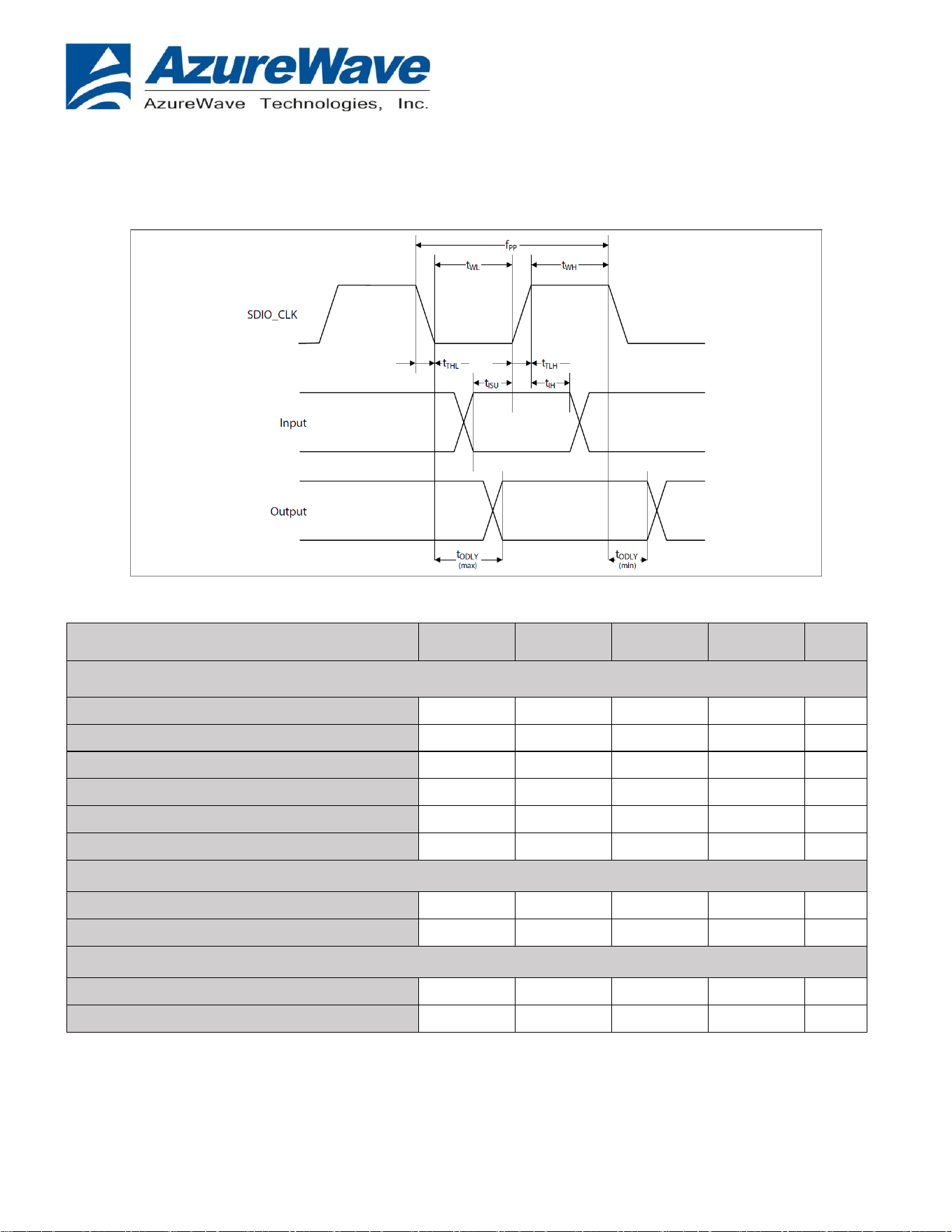
3.4.1 SDIO Host Interface
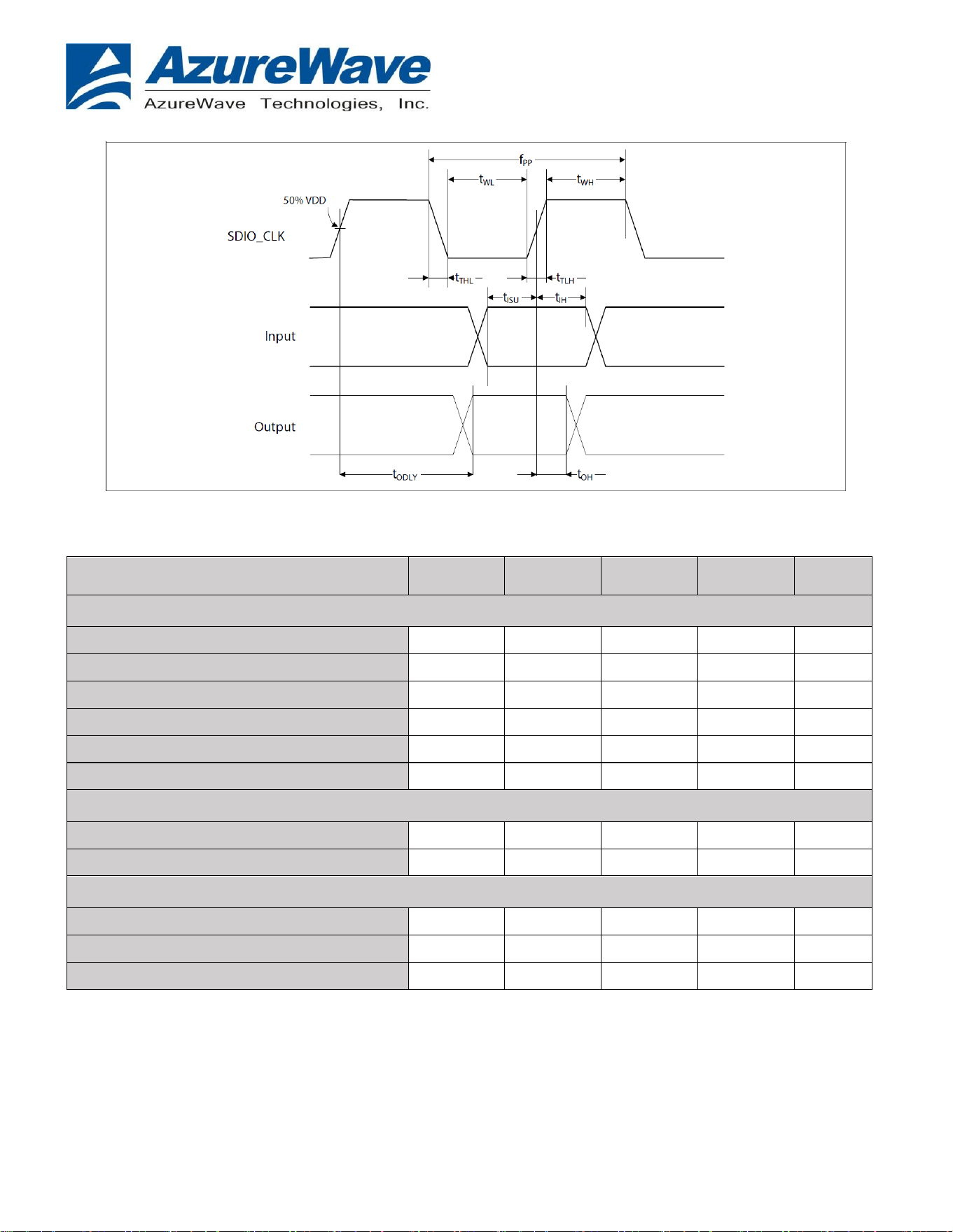
■ SDIO Bus Timing (Default Mode)
SDIO Bus Timing
1
Parameters (Default Mode)
Parameter
Symbol
Minimum
Typical
Maximum
Unit
SDIO CLK (All values are referred to minimum VIH and maximum VIL
2
)
Frequency – Data Transfer mode
f
PP
0
–
25
MHz
Frequency – Identification mode
f
OD
0
–
400
kHz
Clock low time
t
WL
10
–
–
ns
Clock high time
t
WH
10
–
–
ns
Clock rise time
t
TLH
–
–
10
ns
Clock low time
t
THL
–
–
10
ns
Inputs: CMD, DAT (referenced to CLK)
Input setup time
t
ISU
5
–
–
ns
Input hold time
t
IH
5
–
–
ns
Outputs: CMD, DAT (referenced to CLK)
Output delay time – Data Transfer mode
t
ODLY
0
–
14
ns
Output delay time – Identification mode
t
ODLY
0
–
50
ns
Notes:
1. Timing is based on C
L
≤ 40 pF load on CMD and Data.
2. Min (Vih) = 0.7 × VDDIO and max (Vil) = 0.2 × VDDIO.
18
FORM NO.: FR2-015_ A Responsible Department:WBU Expiry Date: Forever
The information contained herein is the exclusive property of AzureWave and shall not be distributed, reproduced, or
disclosed in whole or in part without prior written permission of AzureWave.
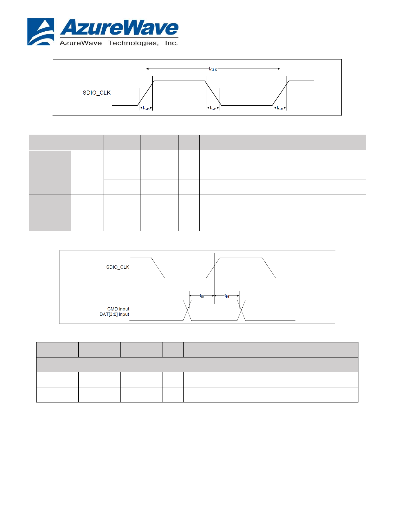
■ SDIO High-Speed Mode Timing
SDIO Bus Timing
1
Parameters (High-Speed Mode)
Parameter
Symbol
Minimum
Typical
Maximum
Unit
SDIO CLK (all values are referred to minimum VIH and maximum VIL
2
Frequency – Data Transfer Mode
f
PP
0
–
50
MHz
Frequency – Identification Mode
f
OD
0
–
400
kHz
Clock low time
t
WL
7
–
–
ns
Clock high time
t
WH
7
–
–
ns
Clock rise time
t
TLH
–
–
3
ns
Clock low time
t
THL
–
–
3
ns
Inputs: CMD, DAT (refer- enced to CLK)
Input setup Time
t
ISU
6
–
–
ns
Input hold Time
t
IH
2
–
–
ns
Outputs: CMD, DAT (refer- enced to CLK)
Output delay time – Data Transfer Mode
t
ODLY
–
–
14
ns
Output hold time
t
OH
2.5
–
–
ns
Total system capacitance (each line)
C
L
–
–
40
pF
Notes:
1. Timing is based on C
L
≤ 40 pF load on CMD and Data.
2. Min (Vih) = 0.7 × VDDIO and max (Vil) = 0.2 × VDDIO.
19
FORM NO.: FR2-015_ A Responsible Department:WBU Expiry Date: Forever
The information contained herein is the exclusive property of AzureWave and shall not be distributed, reproduced, or
disclosed in whole or in part without prior written permission of AzureWave.
■ SDIO Clock Timing (SDR Mode)
SDIO Bus Clock Timing parameters (SDR Modes)
Parameter
Symbol
Minimum
Typical
Unit
Comments
–
t
CLK
40.0
–
ns
SDR12 mode
20.0
–
ns
SDR25 mode
12.5
–
ns
SDR50 mode
–
t
CR
, t
CF
–
0.2 × t
CLK
ns
t
CR
, t
CF
< 2.00 ns (max) @100 MHz, C
CARD
= 10 pF
t
CR
, t
CF
< 0.96 ns (max) @208 MHz, C
CARD
= 10 pF
Duty Cycle
–
30.0
70.0
%
–
■ SDIO Bus Input Timing (SDR Modes)
SDIO Bus Input Timing parameters (SDR Modes)
Symbol
Minimum
Maximum
Unit
Comments
SDR50 Mode
t
IS
3.0
–
ns
C
CARD
= 10 pF, VCT = 0.975 V
t
IH
0.8
–
ns
C
CARD
= 5 pF, VCT = 0.975 V
20
FORM NO.: FR2-015_ A Responsible Department:WBU Expiry Date: Forever
The information contained herein is the exclusive property of AzureWave and shall not be distributed, reproduced, or
disclosed in whole or in part without prior written permission of AzureWave.
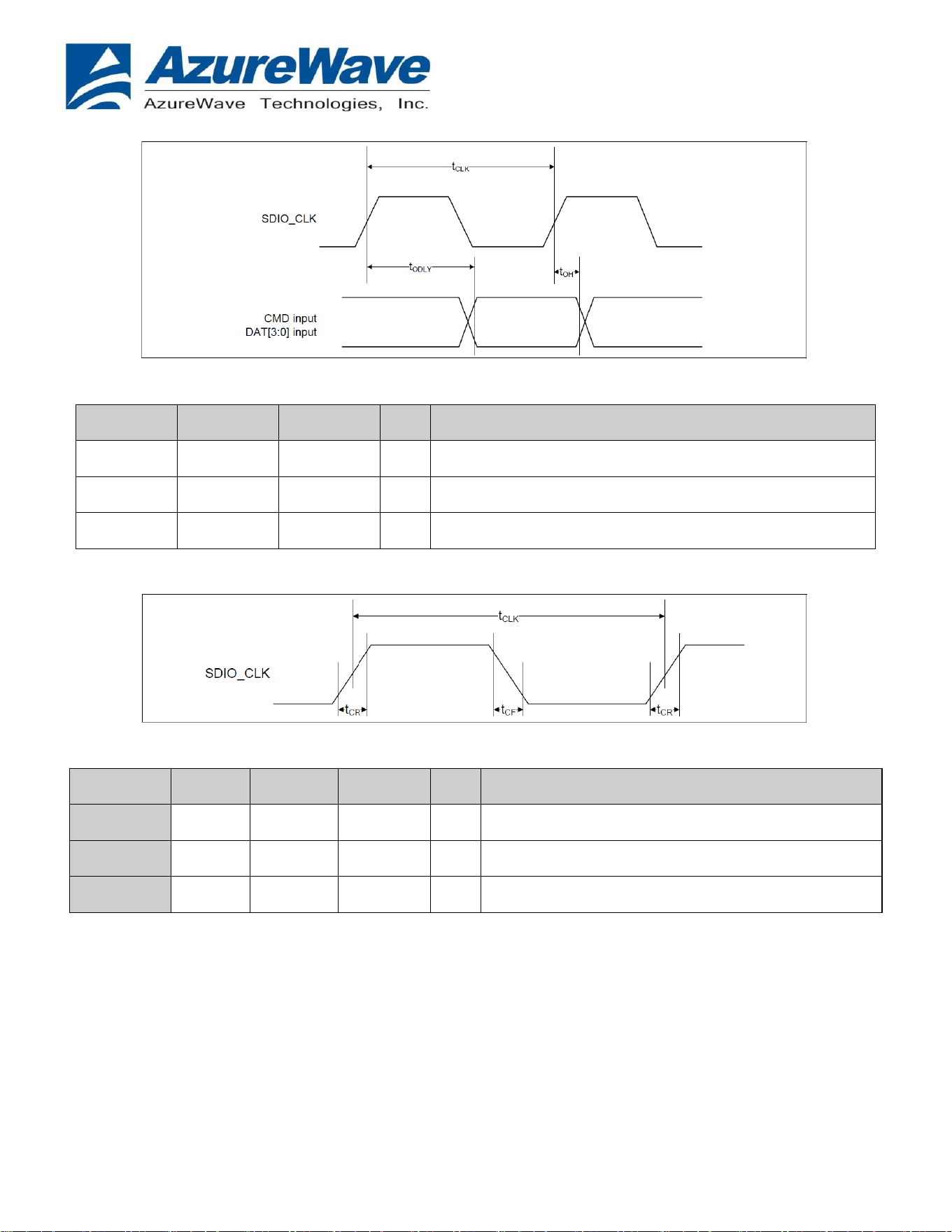
■SDIO Bus Output Timing (SDR Modes up to 80 MHz)
SDIO Bus Output Timing parameters (SDR Modes up to 80 MHz)
Symbol
Minimum
Maximum
Unit
Comments
t
ODLY
–
7.5
ns
t
CLK
≥ 10 ns, C
L
= 30 pF using driver type B for SDR50
t
ODLY
–
14.0
ns
t
CLK
≥ 20 ns, C
L
= 40 pF using for SDR12, SDR25
t
OH
1.5
–
ns
Hold time at the t
ODLY
(min) C
L
= 15 pF
■SDIO Clock Timing (DDR50 Mode)
SDIO Bus Clock Timing parameters (DDR50 Mode)
Parameter
Symbol
Minimum
Typical
Unit
Comments
–
t
CLK
25
–
ns
DDR50 mode
–
t
CR
, t
CF
–
0.2 × t
CLK
ns
t
CR
, t
CF
< 4.00 ns (max) @50 MHz, C
CARD
= 10 pF
Duty Cycle
–
45
55
%
–
21
FORM NO.: FR2-015_ A Responsible Department:WBU Expiry Date: Forever
The information contained herein is the exclusive property of AzureWave and shall not be distributed, reproduced, or
disclosed in whole or in part without prior written permission of AzureWave.
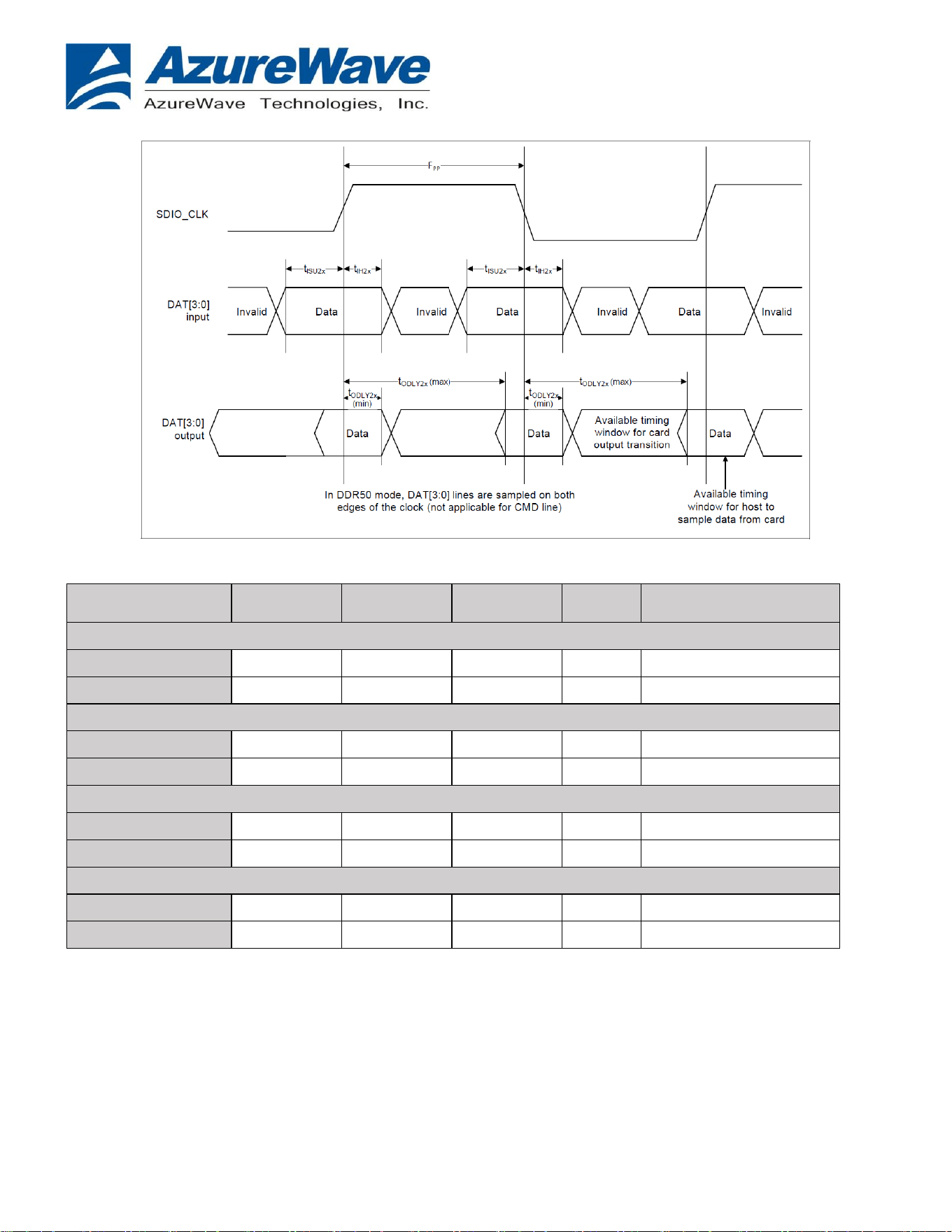
■SDIO Data Timing (DDR50 Mode)
SDIO Bus Timing parameters (DDR50 Mode)
Parameter
Symbol
Minimum
Maximum
Unit
Comments
Input CMD
Input setup Time
t
ISU
6
–
ns
C
CARD
< 10 pF (1 Card)
Input hold Time
t
IH
0.8
–
ns
C
CARD
< 10 pF (1 Card)
Output CMD
Output delay time
t
ODLY
–
13.7
ns
C
CARD
< 30 pF (1 Card)
Output hold time
t
OH
1.5
–
ns
C
CARD
< 15 pF (1 Card)
Input DAT
Input setup Time
t
ISU2x
3
–
ns
C
CARD
< 10 pF (1 Card)
Input hold Time
t
IH2x
0.8
–
ns
C
CARD
< 10 pF (1 Card)
Output DAT
Output delay time
t
ODLY2x
–
7.5
ns
C
CARD
< 25 pF (1 Card)
Output hold time
t
OH2x
1.5
–
ns
C
CARD
< 15 pF (1 Card)
22
FORM NO.: FR2-015_ A Responsible Department:WBU Expiry Date: Forever
The information contained herein is the exclusive property of AzureWave and shall not be distributed, reproduced, or
disclosed in whole or in part without prior written permission of AzureWave.
3.4.2 UART Interface
The BT HCI UART is a standard 4-wire interface (RX, TX, RTS, and CTS) with adjustable baud rates
from 115200 bps to 4.0 Mbps.
The interface features an automatic baud rate detection capability that returns a baud rate selection.
The baud rate may be changed using a vendor-specific UART HCI command.
The UART has a 1040-byte receive FIFO and a 1040-byte transmit FIFO to support EDR. Access to
the FIFOs is through the AHB interface through either DMA or the CPU. The UART supports the
Bluetooth UART HCI H4 specification. The default baud rate is 115.2 Kbaud.
The AW-CM689 UART can perform XON/XOFF flow control and includes hardware support for the
Serial Line Input Protocol (SLIP).
It can also perform wake-on activity. For example, activity on the RX or CTS inputs can wake the
chip from a sleep state.
Normally, the UART baud rate is set by a configuration record downloaded after device reset, or by
automatic baud rate detection, and the host does not need to adjust the baud rate. Support for
changing the baud rate during normal HCI UART operation is included through a vendor-specific
command that allows the host to adjust the contents of the baud rate registers.
The AW-CM689 UARTs operate correctly with the host UART as long as the combined baud rate
error of the two devices is within ±2%.
UART Interface Signals
Pin No
Signal Name
Description
Type
42
BT_UART_TXD
Bluetooth UART Serial Output. Serial data output for the
HCI UART Interface
O
43
BT_UART_RXD
Bluetooth UART Series Input. Serial data input for the
HCI UART Interface
I
41
BT_UART_RTS_N
Bluetooth UART Request-to-Send. Active-low request-
to-send signal for the HCI UART interface
O
44
BT_UART_CTS_N
Bluetooth UART Clear-to-Send. Active-low clear-to-
send signal for the HCI UART interface.
I
23
FORM NO.: FR2-015_ A Responsible Department:WBU Expiry Date: Forever
The information contained herein is the exclusive property of AzureWave and shall not be distributed, reproduced, or
disclosed in whole or in part without prior written permission of AzureWave.
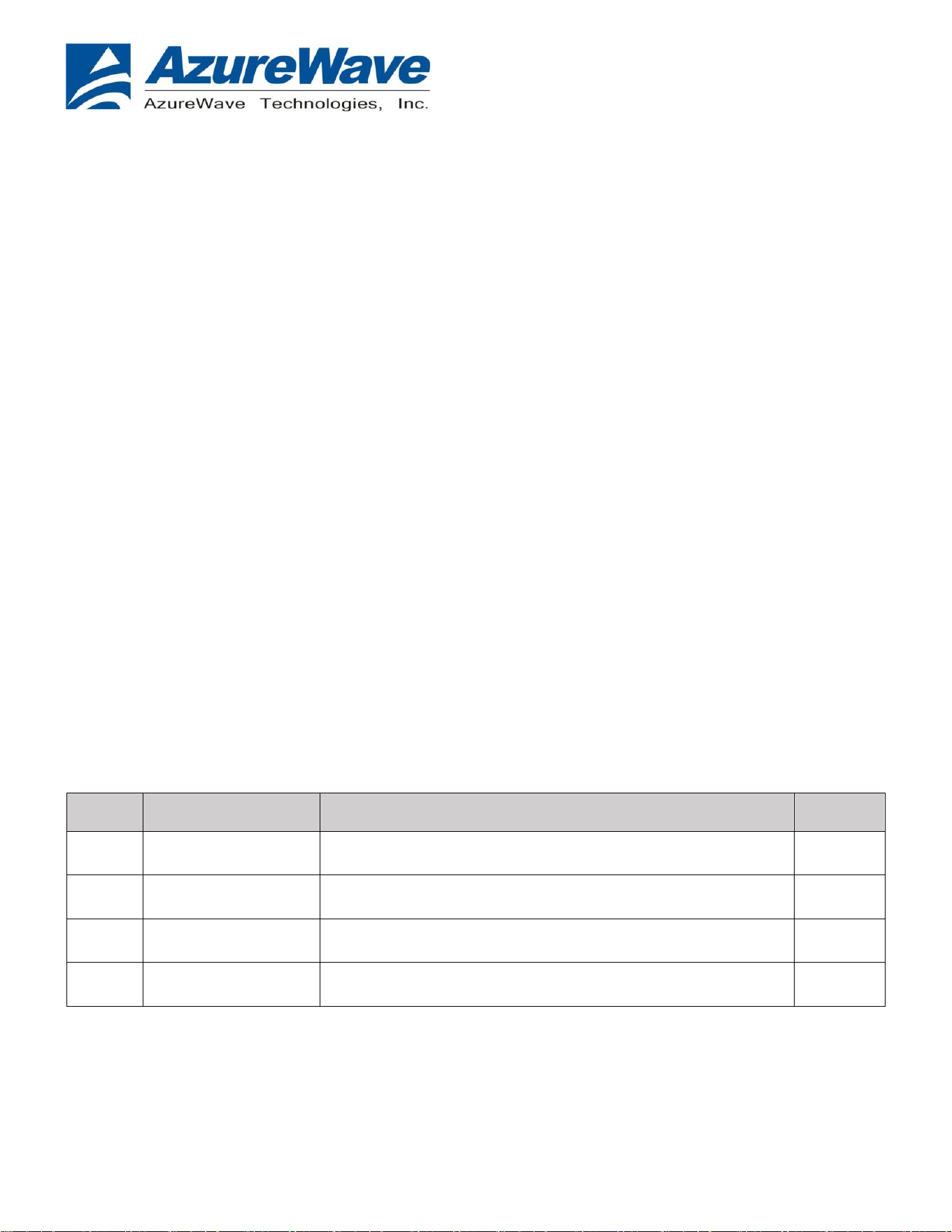
■ UART Timing
UART Timing Specifications
Reference
Characteristics
Minimum
Typical
Maximum
Unit
1
Delay time, BT_UART_CTS_N low to
BT_UART_TXD valid
–
–
1.5
Bit periods
2
Setup time, BT_UART_CTS_N high
before midpoint of stop bit
–
–
0.5
Bit periods
3
Delay time, midpoint of stop bit to
BT_UART_RTS_N high
–
–
0.5
Bit periods

24
FORM NO.: FR2-015_ A Responsible Department:WBU Expiry Date: Forever
The information contained herein is the exclusive property of AzureWave and shall not be distributed, reproduced, or
disclosed in whole or in part without prior written permission of AzureWave.
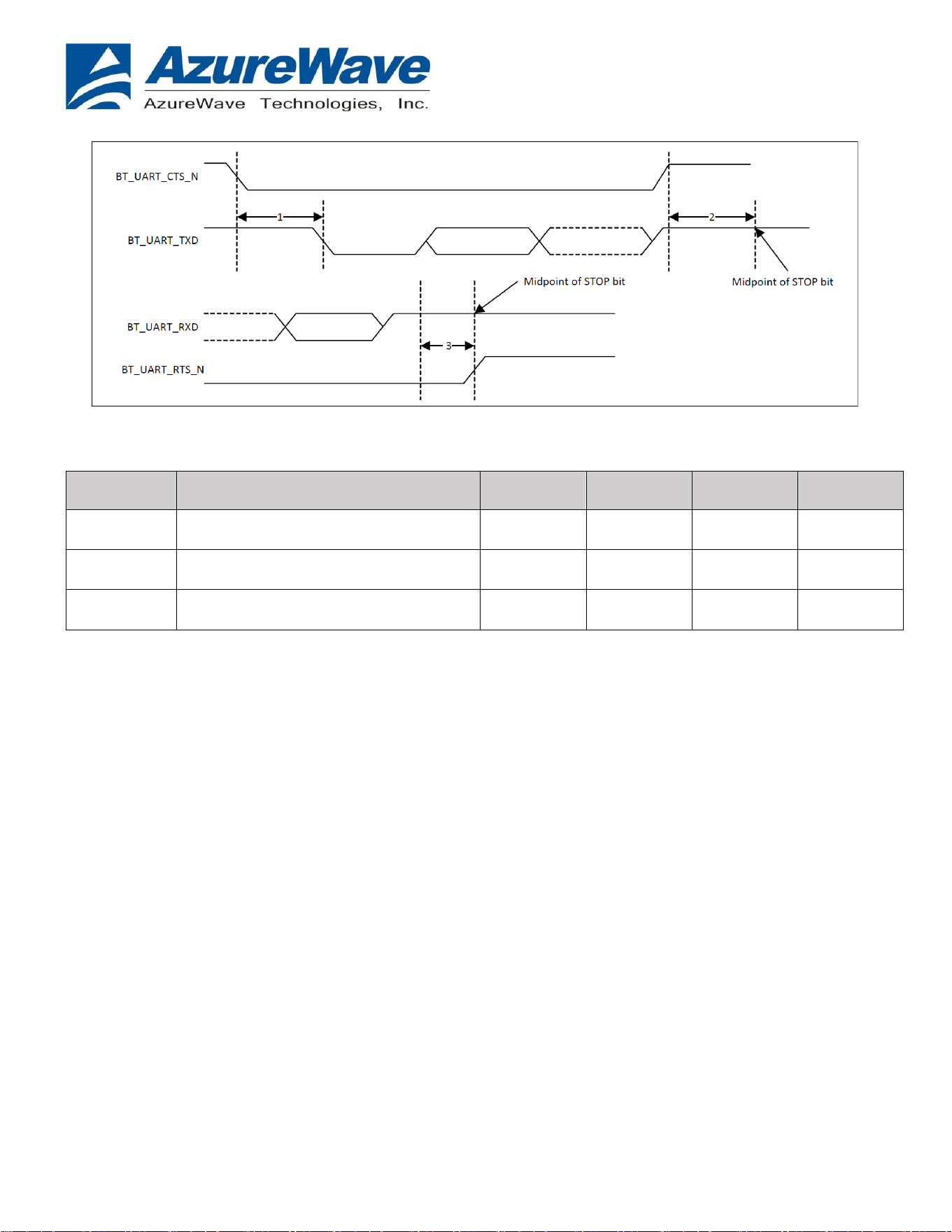
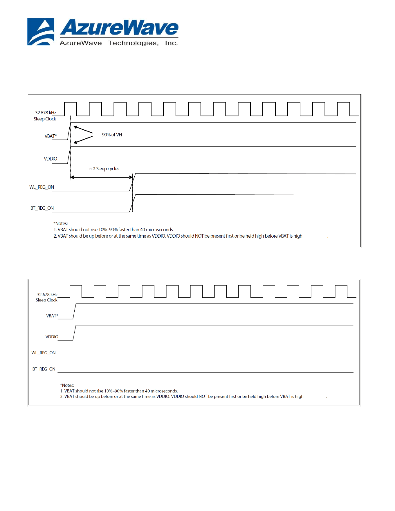
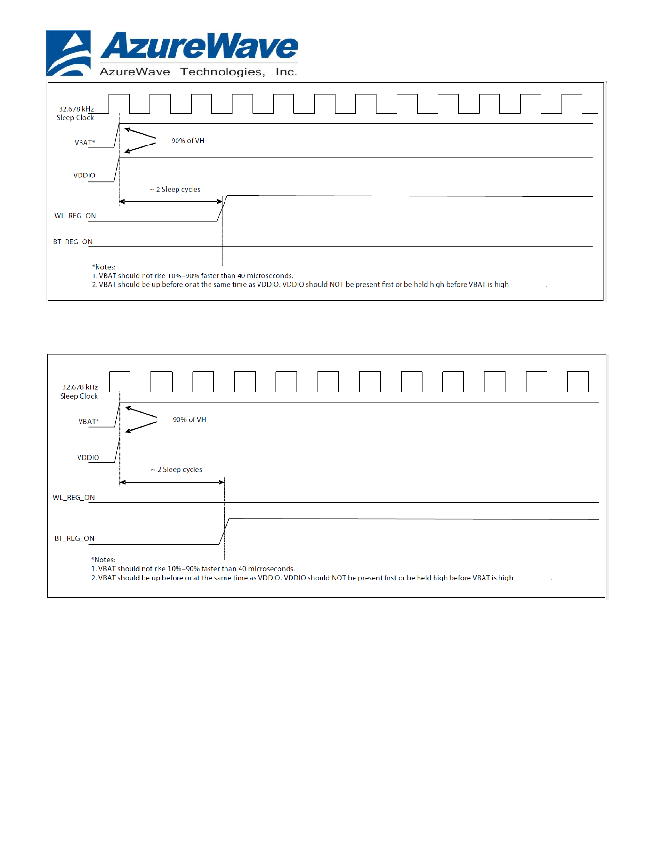
3.5 Power up Timing Sequence
The AW-CM689 has two signals that allow the host to control power consumption by enabling or
disabling the Bluetooth, WLAN, and internal regulator blocks. These signals are described below.
Additionally, diagrams are provided to indicate proper sequencing of the signals for various
operational states. The timing values indicated are minimum required values; longer delays are also
acceptable.
3.5.1 Description of Control Signals
■ WL_REG_ON: Used by the PMU to power-up the WLAN section. It is also OR-gated with the
BT_REG_ON input to control the internal AW-CM689 regulators. When this pin is high, the regulators
are enabled and the WLAN section is out of reset. When this pin is low the WLAN section is in reset.
If both the BT_REG_ON and WL_REG_ON pins are low, the regulators are disabled.
■ BT_REG_ON: Used by the PMU (OR-gated with WL REG ON) to power-up the internal AW-
CM689 regulators. If both the BT_REG_ON and WL_REG_ON pins are low, the regulators are
disabled. When this pin is low and WL_REG_ON is high, the BT section is in reset.
Notes:
1. The AW-CM689 has an internal power-on reset (POR) circuit. The device will be held in reset for a maximum of
110 ms after VDDC and VDDIO have both passed the POR threshold. Wait at least 185 ms after VDDC and VDDIO
are available before initiating Host SDIO or UART accesses.
2. VBAT should not rise 10%–90% faster than 40 microseconds. VBAT should be up before or at the same time as
VDDIO. VDDIO should NOT be present first or be held high before VBAT is high.
25
FORM NO.: FR2-015_ A Responsible Department:WBU Expiry Date: Forever
The information contained herein is the exclusive property of AzureWave and shall not be distributed, reproduced, or
disclosed in whole or in part without prior written permission of AzureWave.
3.5.2 Control Signal Timing diagrams
The AW-CM689 has two signals that enable or disable the Bluetooth and WLAN circuits and the
internal regulator blocks, allowing the host to control power consumption.
WLAN = ON, Bluetooth = ON
WLAN = OFF, Bluetooth = OFF
26
FORM NO.: FR2-015_ A Responsible Department:WBU Expiry Date: Forever
The information contained herein is the exclusive property of AzureWave and shall not be distributed, reproduced, or
disclosed in whole or in part without prior written permission of AzureWave.
WLAN = ON, Bluetooth = OFF
WLAN = OFF, Bluetooth = ON
27
FORM NO.: FR2-015_ A Responsible Department:WBU Expiry Date: Forever
The information contained herein is the exclusive property of AzureWave and shall not be distributed, reproduced, or
disclosed in whole or in part without prior written permission of AzureWave.
3.6 Power Consumption
3.6.1 WLAN
No.
Item
VBAT_IN=3.6 V
Max.
Avg.
1
Pdn
*
0.0021
0.0013
2
Deep Sleep
*
(Not associated with AP)
0.022
0.0023
3
Power Save DTIM 1
*
(2.4GHz)
23.9
0.322
4
Power Save DTIM 3
*
(2.4GHz)
21.2
0.110
5
Power Save DTIM 1
*
(5GHz)
24.3
0.228
6
Power Save DTIM 3
*
(5GHz)
21.2
0.089
Band
(GHz)
Mode
BW
(MHz)
RF
Power
(dBm)
Transmit
Max.
Avg.
2.4
11b@1Mbps
20
18
265
227
11g@54Mbps
20
15
232
198
11n@MCS7
20
15
235
195
5
11a@54Mbps
20
13
280
236
11n@MCS7
20
13
280
238
11ac@MCS8 NSS1
20
10
263
219
Band
(GHz)
Mode
BW(MHz)
Receive
Max.
Avg.
2.4
11b@11Mbps
20
23.2
19.4
11g@54Mbps
20
23.1
20.1
11n@MCS7
20
23.2
21.1
5
11a@54Mbps
20
23.1
22.6
11n@MCS7
20
23.4
23.1
11ac@MCS8 NSS1
20
24.9
23.5
*Current Unit: mA
No.
Item
VDDIO=1.8 V
Max.
Avg.
1
Pdn
*
0.031
0.0003
2
Deep Sleep
*
(Not associated with AP)
0.246
0.137
3
Power Save DTIM 1
*
(2.4GHz)
1.1
0.143
4
Power Save DTIM 3
*
(2.4GHz)
1.0
0.146
5
Power Save DTIM 1
*
(5GHz)
1.1
0.143
6
Power Save DTIM 3
*
(5GHz)
1.0
0.145
Band
(GHz)
Mode
BW
(MHz)
RF
Power
(dBm)
Transmit
Max.
Avg.
2.4
11b@11Mbps
20
18
2.7
2.4
11n@MCS7
20
15
2.6
2.4
28
FORM NO.: FR2-015_ A Responsible Department:WBU Expiry Date: Forever
The information contained herein is the exclusive property of AzureWave and shall not be distributed, reproduced, or
disclosed in whole or in part without prior written permission of AzureWave.
5
11a@54Mbps
20
13
2.8
2.5
11ac@MCS8 NSS1
20
10
2.7
2.5
Band
(GHz)
Mode
BW(MHz)
Receive
Max.
Avg.
2.4
11b@11Mbps
20
0.48
0.47
5
11ac@MCS8 NSS1
20
0.87
0.85
*Current Unit: mA
* The power consumption is based on Azurewave test environment, these data for reference only.
3.6.2 Bluetooth
Test Results
Mode
Packet Type
RF Power
(dBm)
VBAT_IN=3.6 V
Max.
Avg.
Sleep
*
N/A
N/A
37.5
0.0022
Transmit
*
DH5
9.5
25.8
23.5
Receive
*
DH5
N/A
12.9
10.7
Transmit
*
LE
9.4
25.5
23.8
Receive
*
LE
N/A
12.9
12.5
Current Unit: mA
Mode
Packet Type
RF Power
(dBm)
VDDIO=1.8 V
Max.
Avg.
Sleep
*
N/A
N/A
36510
39
Transmit
*
DH5
9.5
333
311
Receive
*
DH5
N/A
304
255
Transmit
*
LE
9.4
319
308
Receive
*
LE
N/A
308
289
Current Unit: uA
* The power consumption is based on Azurewave test environment, these data for reference only
29
FORM NO.: FR2-015_ A Responsible Department:WBU Expiry Date: Forever
The information contained herein is the exclusive property of AzureWave and shall not be distributed, reproduced, or
disclosed in whole or in part without prior written permission of AzureWave.
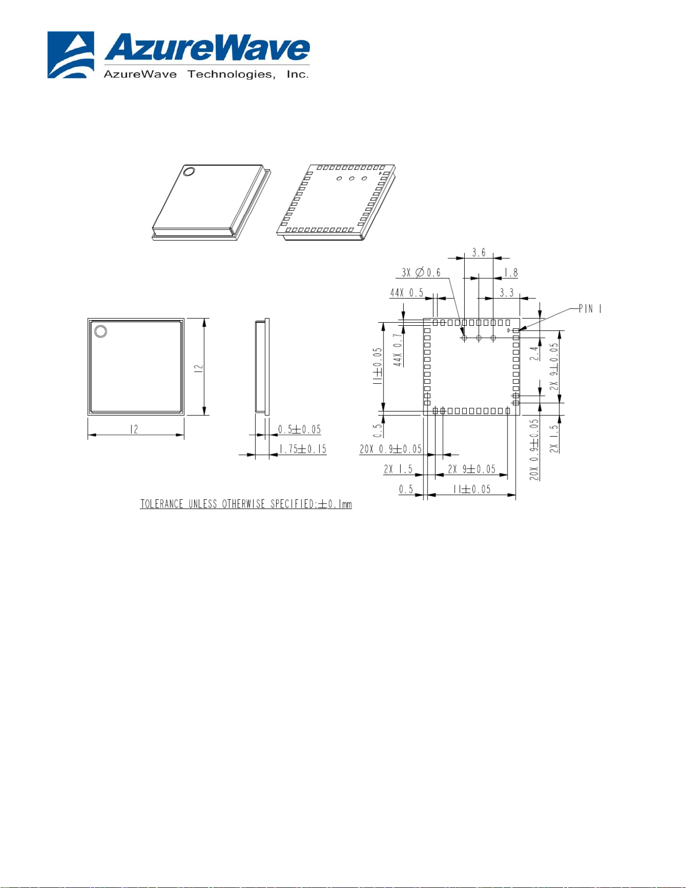
4. Mechanical Information
4.1 Mechanical Drawing
Unit:mm
30
FORM NO.: FR2-015_ A Responsible Department:WBU Expiry Date: Forever
The information contained herein is the exclusive property of AzureWave and shall not be distributed, reproduced, or
disclosed in whole or in part without prior written permission of AzureWave.
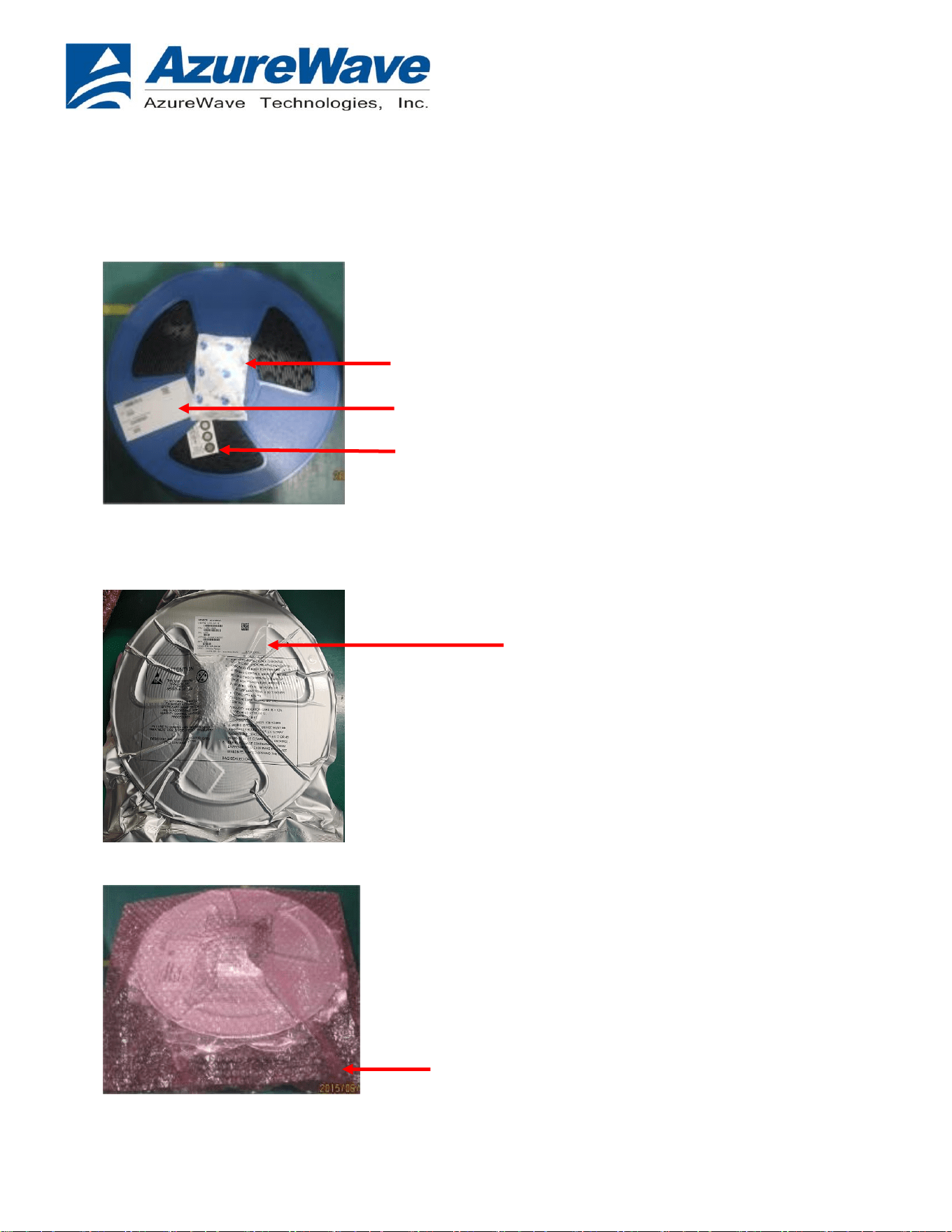
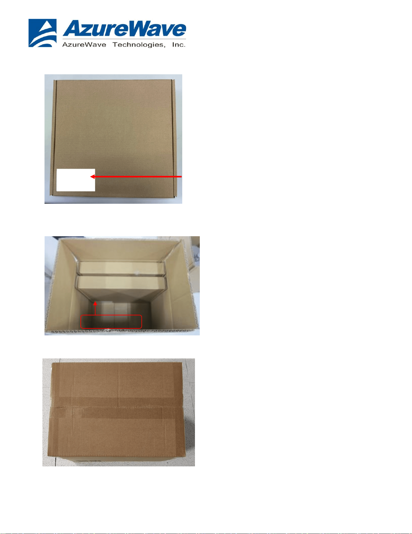
5. Packaging Information
1. One reel can pack 1,500pcs 12x12 LGA modules
2. One production label is pasted on the reel, one desiccant and one humidity indicator card are
put on the reel
3. One reel is put into the anti-static moisture barrier bag, and then one production label is pasted
on the bag
4. A bag is put into the anti-static pink bubble wrap
One production label
One desiccant
One humidity indicator card
One production label
One anti-static pink bubble wrap
31
FORM NO.: FR2-015_ A Responsible Department:WBU Expiry Date: Forever
The information contained herein is the exclusive property of AzureWave and shall not be distributed, reproduced, or
disclosed in whole or in part without prior written permission of AzureWave.
5. A bubble wrap is put into the inner box and then one label is pasted on the inner box
6. 5 inner boxes could be put into one carton
7. Sealing the carton by transparent tape
Production
label
One production label
Production label
32
FORM NO.: FR2-015_ A Responsible Department:WBU Expiry Date: Forever
The information contained herein is the exclusive property of AzureWave and shall not be distributed, reproduced, or
disclosed in whole or in part without prior written permission of AzureWave.
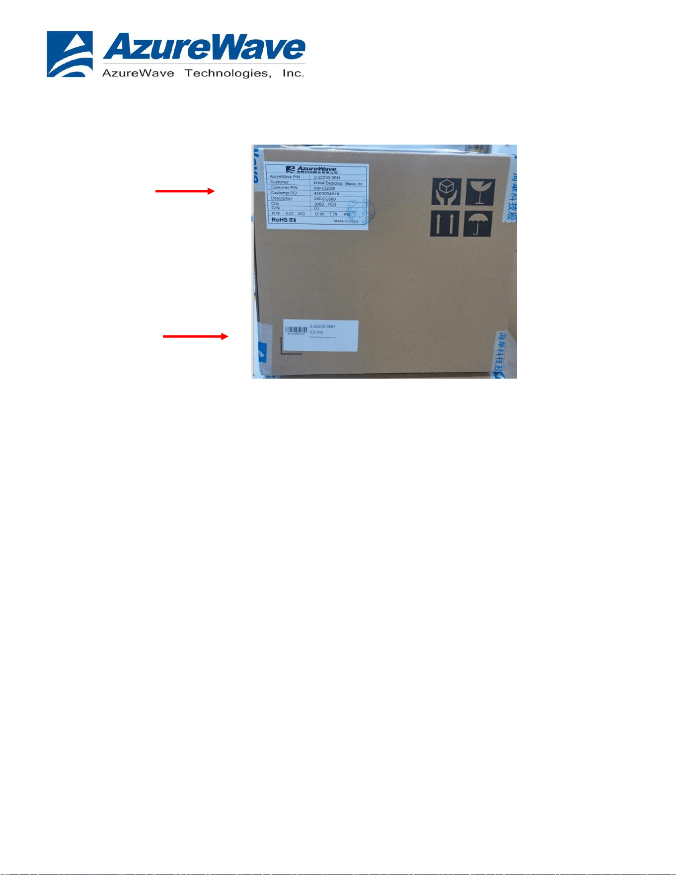
8. One carton label and one box label are pasted on the carton. If one carton is not full, one
balance label pasted on the carton
One carton label
One box label
33
FORM NO.: FR2-015_ A Responsible Department:WBU Expiry Date: Forever
The information contained herein is the exclusive property of AzureWave and shall not be distributed, reproduced, or
disclosed in whole or in part without prior written permission of AzureWave.
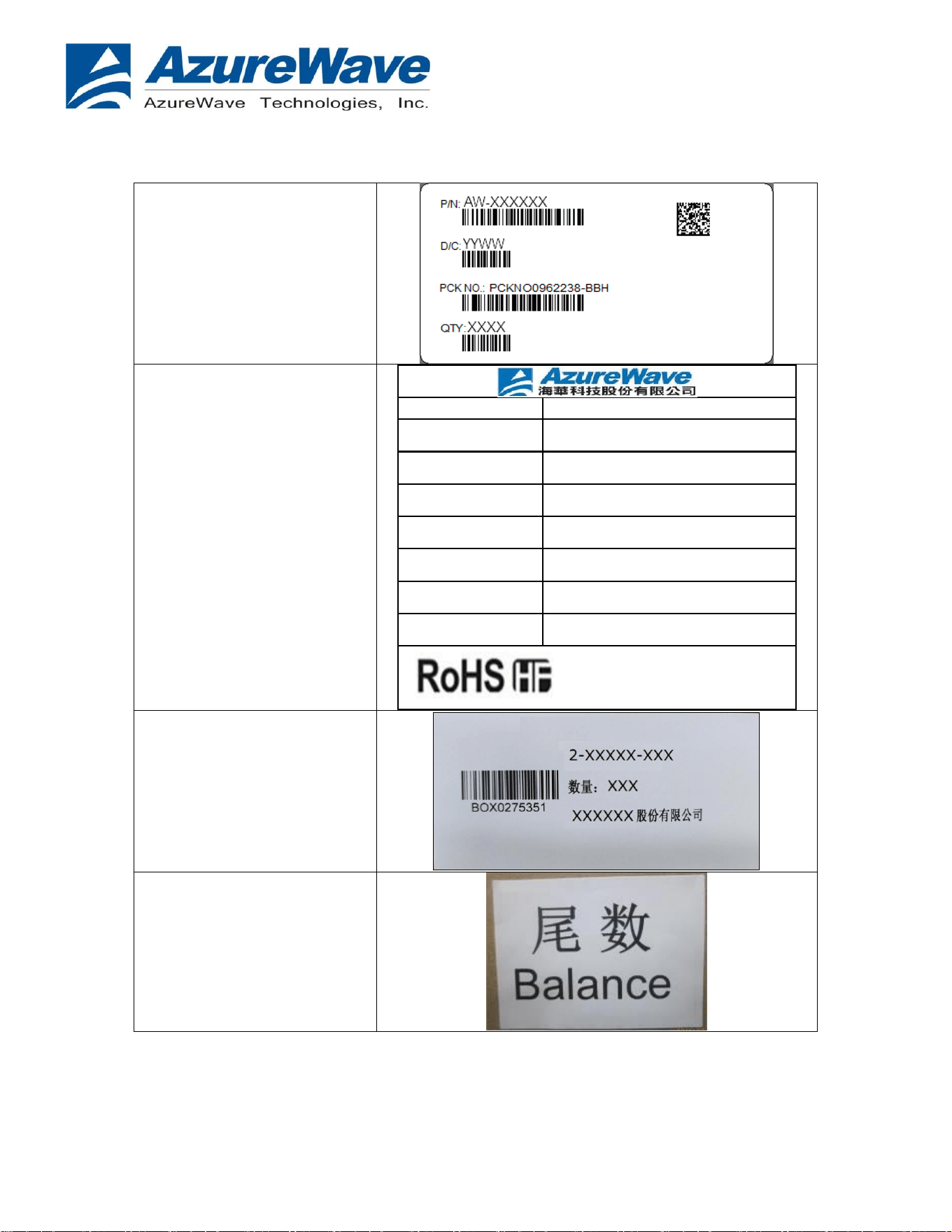
Label Information on the carton
Example of Production
Label
Example of carton label
AzureWave P/N
AW-CM689
Customer
Provided by Sales(由业务提供)
Customer P/N
Provided by Sales(由业务提供)
Customer P/O
Provided by Sales(由业务提供)
Description
AW-CM689
Q'ty
依照实际出货数量
C/N
依实际情况填写
N.W.
G.W.
Made in China
Example of box label
Example of balance label

34
FORM NO.: FR2-015_ A Responsible Department:WBU Expiry Date: Forever
The information contained herein is the exclusive property of AzureWave and shall not be distributed, reproduced, or
disclosed in whole or in part without prior written permission of AzureWave.
6. FCC Statement
This equipment has been tested and found to comply with the limits for a Class B digital device,
pursuant to Part 15 of the FCC Rules. These limits are designed to provide reasonable protection
against harmful interference in a residential installation. This equipment generates, uses and can
radiate radio frequency energy and, if not installed and used in accordance with the instructions, may
cause harmful interference to radio communications. However, there is no guarantee that
interference will not occur in a particular installation. If this equipment does cause harmful
interference to radio or television reception, which can be determined by turning the equipment off
and on, the user is encouraged to try to correct the interference by one of the following measures:
- Reorient or relocate the receiving antenna.
- Increase the separation between the equipment and receiver.
- Connect the equipment into an outlet on a circuit different from that to which the receiver is
connected.
- Consult the dealer or an experienced radio/TV technician for help.
This device complies with Part 15 of the FCC Rules. Operation is subject to the following two
conditions:
(1) This device may not cause harmful interference, and
(2) This device must accept any interference received, including interference that may cause
undesired operation.
FCC Caution: Any changes or modifications not expressly approved by the party responsible for
compliance could void the user's authority to operate this equipment.
This equipment complies with FCC radiation exposure limits set forth for an uncontrolled environment.
This equipment must be installed and operated with a minimum separation distance of 20 cm
between the radiator and your body. This transmitter must not be co-located or operated in
conjunction with any other antenna or transmitter unless additional evaluation is performed and a
separate FCC authorization is obtained.
In the event that these conditions cannot be met (for example certain laptop configurations or co-
location with another transmitter), then the FCC authorization is no longer considered valid and the
FCC ID cannot be used on the final product. In these circumstances, the OEM integrator will be
responsible for re-evaluating the end product (including the transmitter) and obtaining a separate
FCC authorization.
If the FCC ID is not visible when the module is installed inside the host device, the exterior of the
host device must display a label indicating the FCC ID of the module.
The label must include the following statement:
"Contains Transmitter Module FCC ID: TLZ-CM689"
Alternatively, the label may state: "Contains FCC ID: TLZ-CM689"

35
FORM NO.: FR2-015_ A Responsible Department:WBU Expiry Date: Forever
The information contained herein is the exclusive property of AzureWave and shall not be distributed, reproduced, or
disclosed in whole or in part without prior written permission of AzureWave.
Integration Instructions for OEM Integrators
The module is limited to OEM installation only.
The module is limited to installation in mobile or fixed applications.
The OEM integrator is responsible for ensuring that the end user manual does not contain
instructions on how to remove or install the module.
A separate FCC authorization is required for all other operating configurations, including portable
configurations with respect to Part 2.1093 and different antenna configurations.
Only antennas of the same type and equal or lower gain as those approved in this filing may be used.
The OEM integrator is responsible for ensuring that the final host product complies with the
applicable Part 15B requirements.
The end user manual must include all required regulatory information and warnings as provided in
this document.
The module must be installed in accordance with the instructions provided in this document.