HELTEC/
AUTOMATION
AUTOMATION
/HELTEC
https://heltec.org
Documents
Rev. 1.0
P 2/23
May 2024
Heltec Automation © Limited standard files
Document version
Version
Time
Description
Remark
Rev. 1.0
2024-10-16
P-Development version
Richard
Rev. 2.0
2025-12-17
V2
Shaffer, Richard
Copyright Notice
All contents in the files are protected by copyright law, and all copyrights are reserved by Chengdu
Heltec Automation Technology Co., Ltd. (hereinafter referred to as Heltec). Without written
permission, all commercial use of the files from Heltec are forbidden, such as copy, distribute,
reproduce the files, etc., but non-commercial purpose, downloaded or printed by individual are
welcome.
Disclaimer
Chengdu Heltec Automation Technology Co., Ltd. reserves the right to change, modify or improve
the document and product described herein. Its contents are subject to change without notice.
These instructions are intended for you use.
HELTEC/
AUTOMATION
AUTOMATION
/HELTEC
https://heltec.org
Documents
Rev. 1.0
P 3/23
May 2024
Heltec Automation © Limited standard files
目录
HT-HC01
V2
..................................................................................................................................... 1
Document version..........................................................................................................................2
Copyright Notice............................................................................................................................ 2
Disclaimer...................................................................................................................................... 2
1 Description
.......................................................................................................................... 4
1.1 Overview
..........................................................................................................................................4
1.2 Features
...........................................................................................................................................5
1.3 Application .......................................................................................................................5
2 Pin Description
..................................................................................................................6
3 Specifications
....................................................................................................................9
3.1 General Specifications ............................................................................................................ 9
3.2 Electrical characteristics .................................................................................................... 10
3.3 RF characteristics....................................................................................................................12
4 Reference Design
...........................................................................................................12
4.1 SPI ......................................................................................................................................12
4.2 SDIO
...................................................................................................................................13
4.3 Requirements and considerations ....................................................................13
5 Hardware Dimensions ................................................................................................. 15
5.1 Dimensions
...................................................................................................................................15
5.2 PCB footprint
...............................................................................................................................15
6 Resource .............................................................................................................................16
6.1Relevant resources...................................................................................................................16
6.2 Heltec Contact Information
................................................................................................ 16
HELTEC/
AUTOMATION
AUTOMATION
/HELTEC
https://heltec.org
Documents
Rev. 1.0
P 4/23
May 2024
Heltec Automation © Limited standard files
1 Description
1.1 Overview
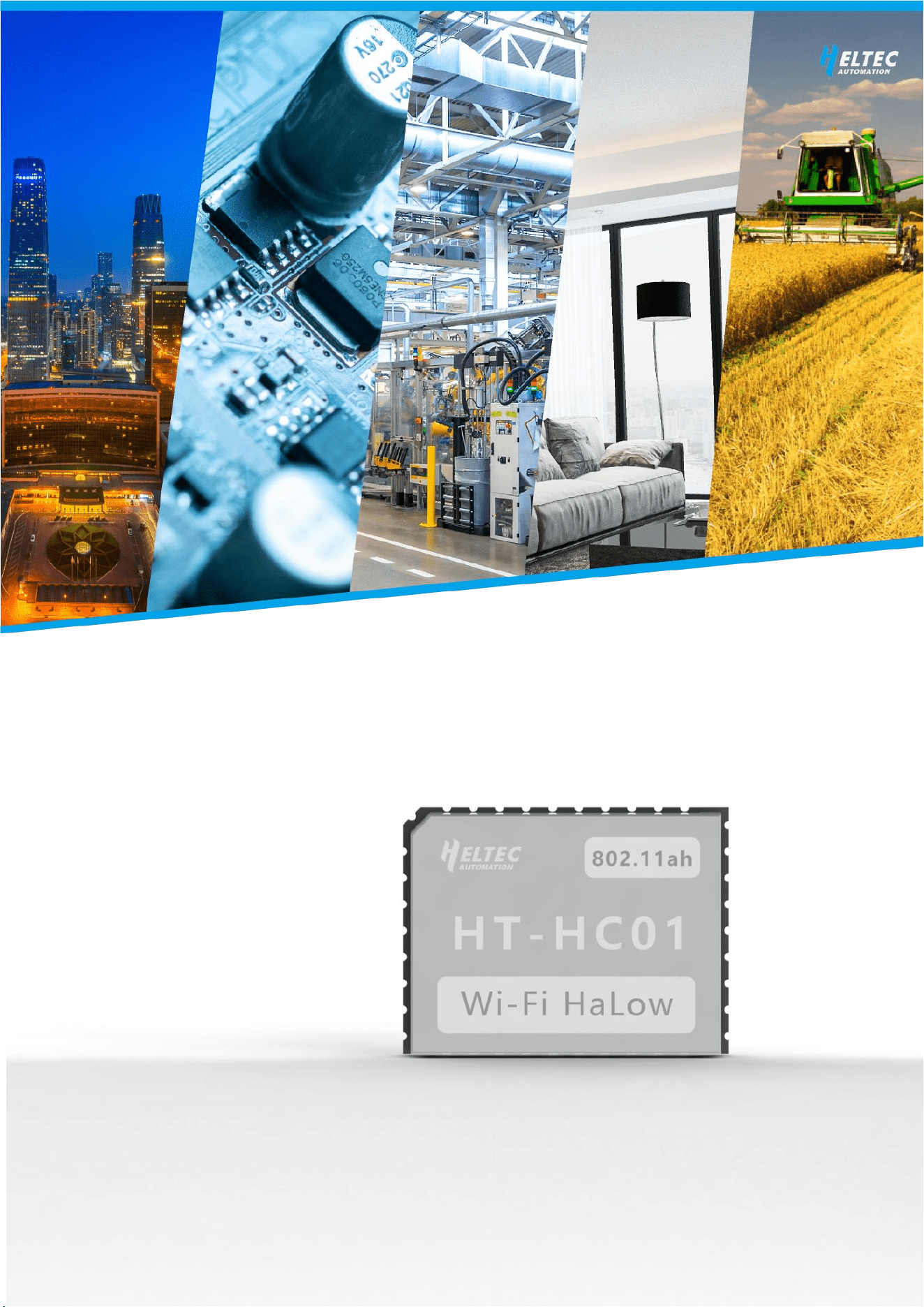
HT-HC01 is a Wi-Fi HaLow module with excellent RF performance, which operates in863-870
and 902-928MHz
①
, with maximum data rates of 32.5Mbps and up to 1-2km transmission
range.
HT-HC01 uses LLC package, small size and rich pin, can be very convenient to integrate in a
variety of PCB. It includes ultra-long range PA, high linear LNA, T/R switching, 32 MHz crystal
oscillator, and is designed to simplify Wi-Fi HaLow connectivity to external hosts for
applications.
HT-HC01 meets IEEE 802.11ah standard, which is specifically designed for battery-operated
devices, allowing them to remain in longer sleep and idle states without frequent wake-ups.
This significantly reduces power consumption and extends the device's battery life.As a result,
HT-HC01 becomes an ideal choice for Internet of Things (IoT) devices and other
battery-powered equipment.
①
The hardware versions are different for 868MHz and 915MHz.
HELTEC/
AUTOMATION
AUTOMATION
/HELTEC
https://heltec.org
Documents
Rev. 1.0
P 5/23
May 2024
Heltec Automation © Limited standard files
1.2 Features
Long-range transmission, up to 1km or and further within the visual distance.
Channel bandwidth options of 1/2/4/8 MHz.
High data rate, single-stream max rate of 32.5 Mbps @ 8 MHz.
Support Sub-1 GHz frequency bands, frequency range: US 902~928 MHz.
Max output power:29dBm.
802. 11ah OFDM PHY supporting WFA HaLow certification.
802. 11ah MAC supporting WFA HaLow certification.
Support for various interface options, include
SDIO 2.0, 2* UART..
Hibernate mode (internal / external wake).
Integrated DC-DC converter supporting VDD supply from 3.0V to 3.6V, and VFEM supply
from 5V.
1.27mm stamp hole design, easy to integrate.
Wide spectrum of security features.

HELTEC/
AUTOMATION
AUTOMATION
/HELTEC
https://heltec.org
Documents
Rev. 1.0
P 7/23
May 2024
Heltec Automation © Limited standard files
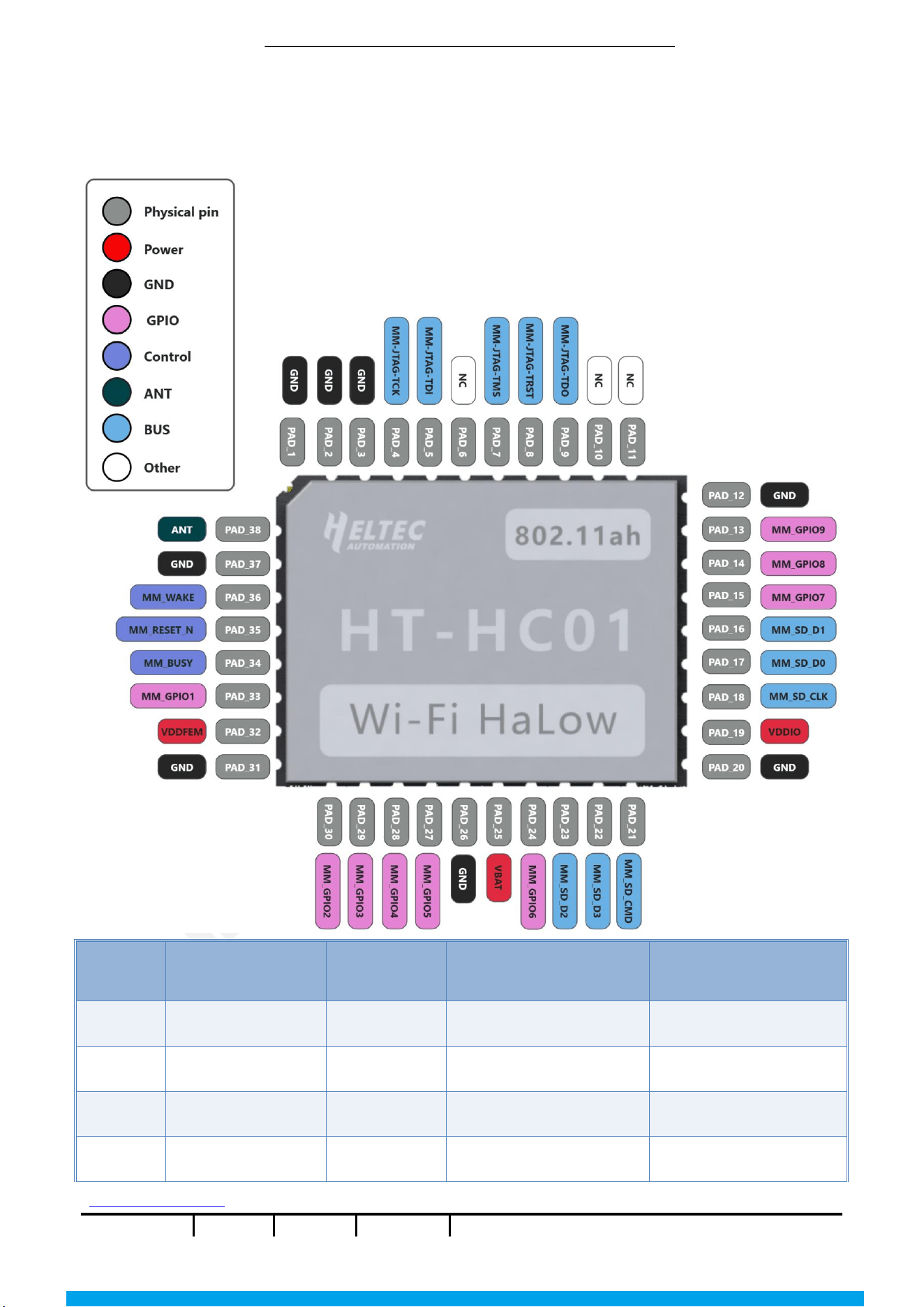
PAD_5
MM_JTAG_TDI
I
JTAG Data In
PAD_6
NC
NC
PAD_7
MM_JTAG_TMS
I
JTAG Mode Select
PAD_8
MM_JTAG_TRST_N
I
JTAG Reset
PAD_9
MM_JTAG_TDO
O
JTAG Data Out
PAD_10
NC
I/O
PAD_11
NC
I/O
PAD_12
GND
POWER
Ground
PAD_13
MM_GPIO_9
I/O
General Purpose IO9
PAD_14
MM_GPIO_8
I/O
General Purpose IO8
PAD_15
MM_GPIO_7
I/O
General Purpose IO7
UART1
_
TX
[4]
PAD_16
MM_SDIO_D1
I/O
SDIO D1
SPI_INT
PAD_17
MM_SDIO_DO
I/O
SDIO D0
SPI_MISO
PAD_18
MM_SDIO_CLK
I/O
SDIO Clock
SPI_SCK
PAD_19
MM_VDD_IO
POWER
3.3V VDD_IO Supply
PAD_20
GND
POWER
Ground
PAD_21
MM_SDIO_CMD
I/O
SDIO Command
SPI_MOSI
PAD_22
MM_SDIO_D3
I/O
SDIO D3
SPI_CS
PAD_23
MM_SDIO_D2
I/O
SDIO D2
PAD_24
MM_GPIO_6
I/O
General Purpose IO6
UART1
_
RX
[4]
PAD_25
VBAT
POWER
3.3V VBAT Supply
PAD_26
GND
POWER
Ground
PAD_27
MM_GPIO_5
I/O
General Purpose IO5
I2C
_
SCL
[4]

HELTEC/
AUTOMATION
AUTOMATION
/HELTEC
https://heltec.org
Documents
Rev. 1.0
P 8/23
May 2024
Heltec Automation © Limited standard files
PAD_28
MM_GPIO_4
I/O
General Purpose IO4
I2C
_
SDA
[4]
PAD_29
MM_GPIO_3
I/O
General Purpose IO3
UART0_TX, PWM1_3
[4]
PAD_30
MM_GPIO_2
I/O
General Purpose IO2
UART0_RX, PWM1_2
[4]
PAD_31
GND
POWER
Ground
PAD_32
VDD_FEM
POWER
5V Frontend Supply
PAD_33
MM_GPIO_1
I/O
General Purpose IO1
PWM1
_
1
[4]
PAD_34
MM_GPIO_0
O
Wi-Fi BUSY
PAD_35
RESET_N
I
System Reset
PAD_36
WAKE
I
Wake
PAD_37
GND
POWER
Ground
PAD_38
ANT_1
ANALOG
Antenna
NOTE:
JTAG pins should be tied to GND via a 10k pull down resistor
All unused GPIO should be tied to GND via a 10k pull down resistor
All SDIO bus pins should be pull up with a 10k-100k resistor as per the the SDIO
standard
Pending software support
Supplied from VBAT domain. Other digital pins are driven by VDDIO domain.
HELTEC/
AUTOMATION
AUTOMATION
/HELTEC
https://heltec.org
Documents
Rev. 1.0
P 9/23
May 2024
Heltec Automation © Limited standard files
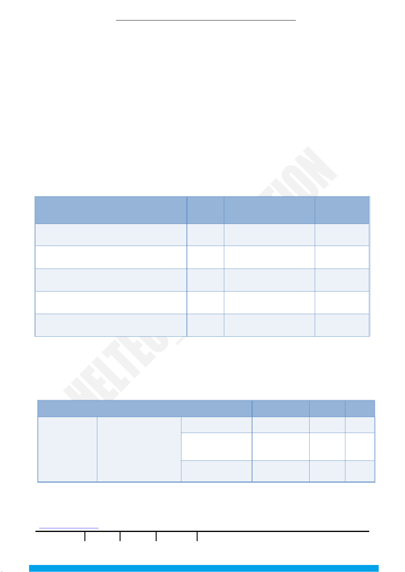
3 Specifications
3.1 General Specifications
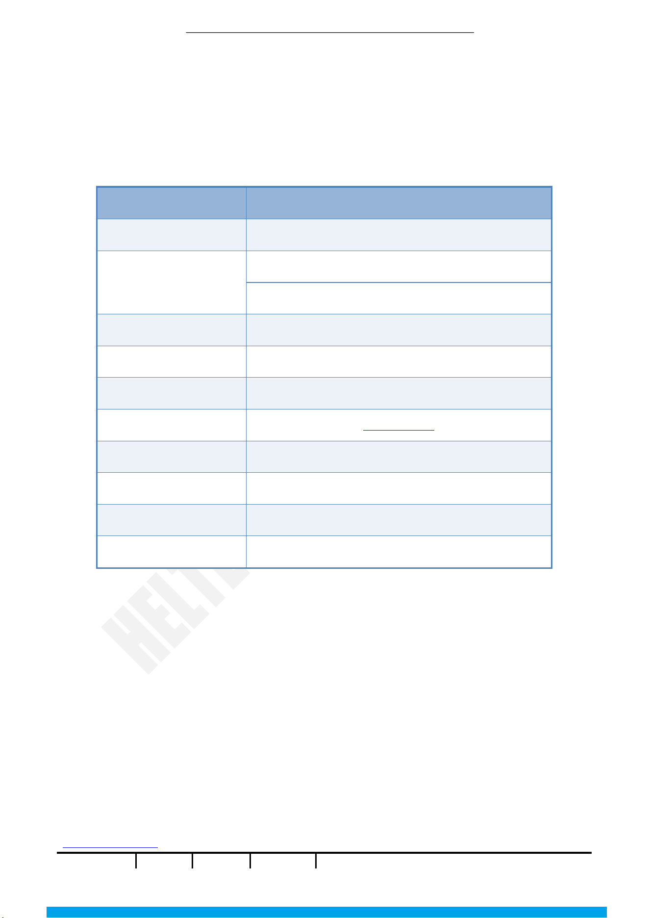
Table 3.1 General specifications
Parameters
Description
Main Chip
MM6108IQ
Power Supply
VBAT/VDD_IO : 3.0~3.6V
VDD_FEM : 3.0~5.25V
HaLow Standard
IEEE 802.11ah
Band Width
1/2/4/8MHz
Interface
38 Header Pins
Power consumption
See table 3.2.4
Operating temperature
-40 ~ 85℃
Operating humidity
10%~90%, no-condensing
Dimensions
18.5*14*2.6mm
Data Rate
Maximum physical air interface rate: 32 Mbps
HELTEC/
AUTOMATION
AUTOMATION
/HELTEC
https://heltec.org
Documents
Rev. 1.0
P 10/23
May 2024
Heltec Automation © Limited standard files
3.2 Electrical characteristics
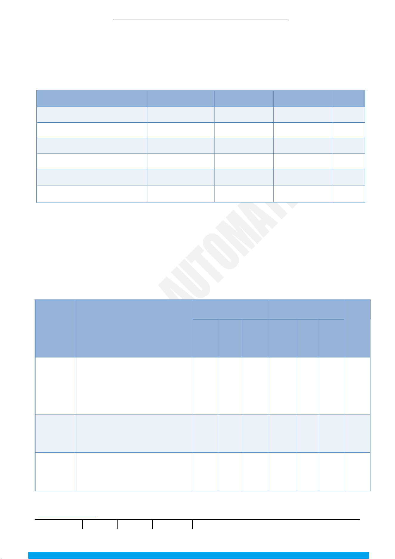
3.2.1 Absolute max ratings
Stress beyond absolute maximum ratings may cause permanent damage to
the module. Functional operation is guaranteed for recommended operation conditions only.
Operation of the device outside the recommended conditions may result in a reduced lifetime
and/or reliability problems (even if the absolute maximum ratings are not exceeded).
Table3.2.1 Absolute max ratings
Parameter
Min
Max
Unit
VBAT voltage
-0.3
4.3
V
VDD_FEM voltage
-0.3
5.5
V
Voltage on digital I/O pin
-0.3
4.3
V
Voltage on analog/RF pin
-0.3
1.2
V
Storage temperature
-40
125
°C
3.2.2 Immunity
Table3.2.2 Immunity
Parameter
Min
Max
Unit
Electrostatic
discharge(ESD)
performance
Human body model
(H3M).perANSI/ESDA/JED
EC JS001
Charged device model
(CDM).perJESD22-C101
RF Input
-1000
1000
V
All pins except RF
Input
-2000
2000
V
All pins
-500
500
V
HELTEC/
AUTOMATION
AUTOMATION
/HELTEC
https://heltec.org
Documents
Rev. 1.0
P 11/23
May 2024
Heltec Automation © Limited standard files
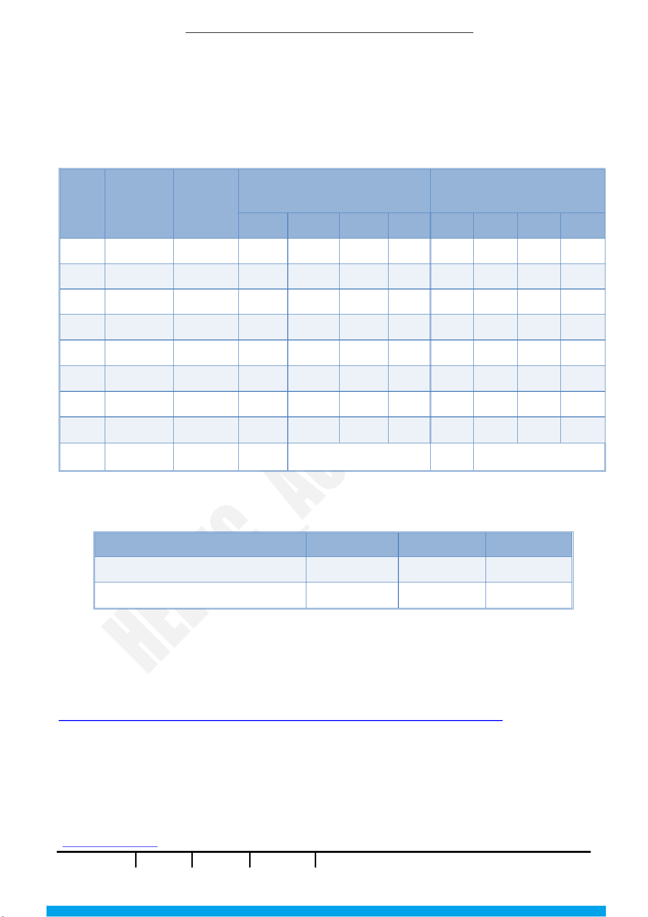
3.2.3 Recommended operating conditions
Table3.2.3 Recommended operating conditions
Parameter
Min
Type
Max
Unit
Ambient temperature
-40
25
85
°C
VBAT
3.0
3.3
3.6
V
VDD_FEM
3.0
5.0
5.25
V
VDD_IO
1.62
3.3
3.6
V
Digital I/O voltage
0
3.3
VD DI O
V
RESET / WAKE I/O Voltage
0
3.3
VBAT
V
3.2.4 Power consumption
3.2.4.1 Sleep Power
Table3.2.4.3 Sleep power
Mode
Condition
VBAT/VDD_IO =3.3V
VDD_FEM =5V
VBAT
VFEM
Unit
Min
TYP
Max
Min
TYP
Max
Snooze
RC Oscillator on, Memory
retained, configurable wake up
timer
9.5
27
370
1.2
µA
Deep sleep
RC Oscillator on, configurable
wake up timer
0.8
1
1.8
1.2
µA
Hibernate
Power off, wait for external
interrupt
0.03
0.05
1
1.2
µA
HELTEC/
AUTOMATION
AUTOMATION
/HELTEC
https://heltec.org
Documents
Rev. 1.0
P 12/23
May 2024
Heltec Automation © Limited standard files
3.3 RF characteristics
3.3.1 Receiver sensitivities
Table3.3.1 Receiver sensitivities
MCS
index
Modulation
scheme
Coding
rate
Phy rate (kbps) per BW
Minimum Receive sensitivity
(dBm) per BW
1MHz
2MHz
4MHz
8MHz
1MHz
2MHz
4MHz
8MHz
0
BPSK
1/2
333
722
1500
3250
-105
-103
-101
-97
1
QPSK
1/2
667
1444
3000
6500
-102
-100
-97
-93
2
QPSK
3/4
1000
2167
4500
9750
-99
-97
-95
-91
3
16-QAM
1/2
1333
2889
6000
13000
-96
-94
-91
-88
4
16-QAM
3/4
2000
4333
9000
19500
-93
-90
-88
-85
5
64- QAM
2/3
2667
5778
12000
26000
-89
-87
-84
-80
6
64- QAM
3/4
3000
6500
13500
29250
-88
-85
-83
-79
7
64- QAM
5/6
3333
7222
15000
32500
-87
-84
-81
-77
10
BPSK
1/2 x 2
167
N/A
-107
N/A
3.3.2 Transmission power
Table3.3.2 Transmission power
Tx output power (1/2/4/8 MHz BW)
Min (dBm)
Typical (dBm)
Max (dBm)
MCS 0
26
29
26
MCS 7
22
23
24
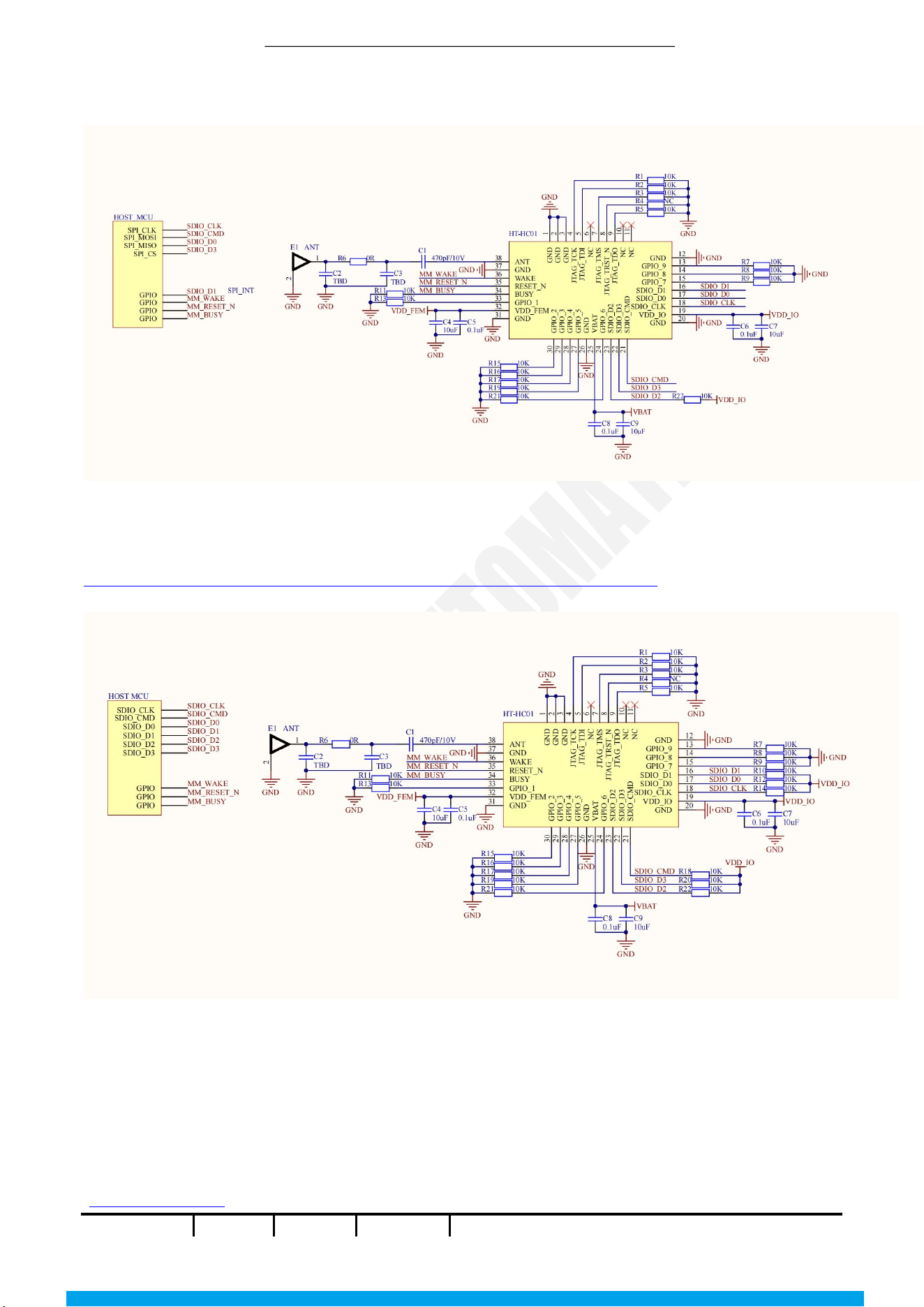
4 Reference Design
4.1 SPI
https://resource.heltec.cn/download/HT-HC01/Reference_design/SPI.PDF
HELTEC/
AUTOMATION
AUTOMATION
/HELTEC
https://heltec.org
Documents
Rev. 1.0
P 13/23
May 2024
Heltec Automation © Limited standard files
4.2 SDIO
https://resource.heltec.cn/download/HT-HC01/Reference_design/SDIO.PDF
4.3 Requirements and considerations
4.3.1 SDIO host requirements
The host should support SDIO v2.0 with SDIO clock speeds of up to 50 MHz. Slower clock
HELTEC/
AUTOMATION
AUTOMATION
/HELTEC
https://heltec.org
Documents
Rev. 1.0
P 14/23
May 2024
Heltec Automation © Limited standard files
speeds will impact the maximum achievable throughput.
At a minimum, 2 x GPIOs are required as a CMOS output to drive the RESET and WAKE
signals. If power save is used, a third GPIO is needed, set as a CMOS input to receive the
BUSY signal from the module.
The SDIO data and command lines should be pulled up with 10k-100k resistors as per the
SDIO 2.0 specification.
4.3.2 SPI host requirements
When selecting a CPU host to interface via SPI to the MM6108-MF08551
module, consider the following recommendations to achieve the best throughput::
The host should support level-triggered interrupts.
The host should support full-duplex SPI mode.
The host should support DMA backed transactions on the SPI bus.
Standard SPI can achieve up to 25 Mbps at 50 MHz but this will reduce significantly if there is
no DMA support. For example, an SPI interface with an 8-byte buffer per transaction might
only achieve 2Mbps throughput on the SPI
bus.
4.3.3 Power management
MM6108-MF08551 module power is derived from a 3.0 to 3.6V supply provided on pins VBAT
and VDD_FEM. VBAT powers the internal circuitry of the MM6108 and VDD_FEM powers the
on-board ultra-long-range power amplifler.
VDDIO sets the IO voltage of the MM6108 and should be connected to the same power supply
as the host MCU.
There are no strict power-up sequencing requirements, however the voltage on VDDIO must
HELTEC/
AUTOMATION
AUTOMATION
/HELTEC
https://heltec.org
Documents
Rev. 1.0
P 15/23
May 2024
Heltec Automation © Limited standard files
not exceed VBAT.
4.3.4 Digital interfaces
All unused digital IO pins must be pulled up or down to ensure they do not float. Failure to do
so will result in a higher leakage current on the VDDIO supply.
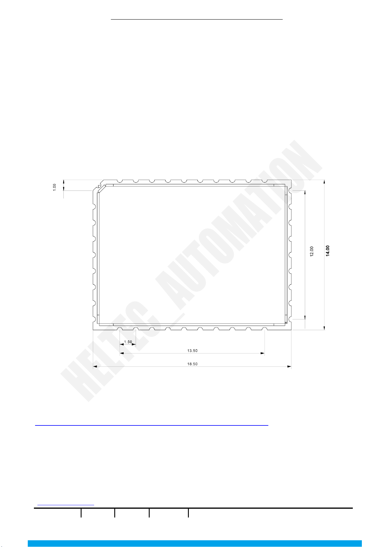
5 Hardware Dimensions
5.1 Dimensions
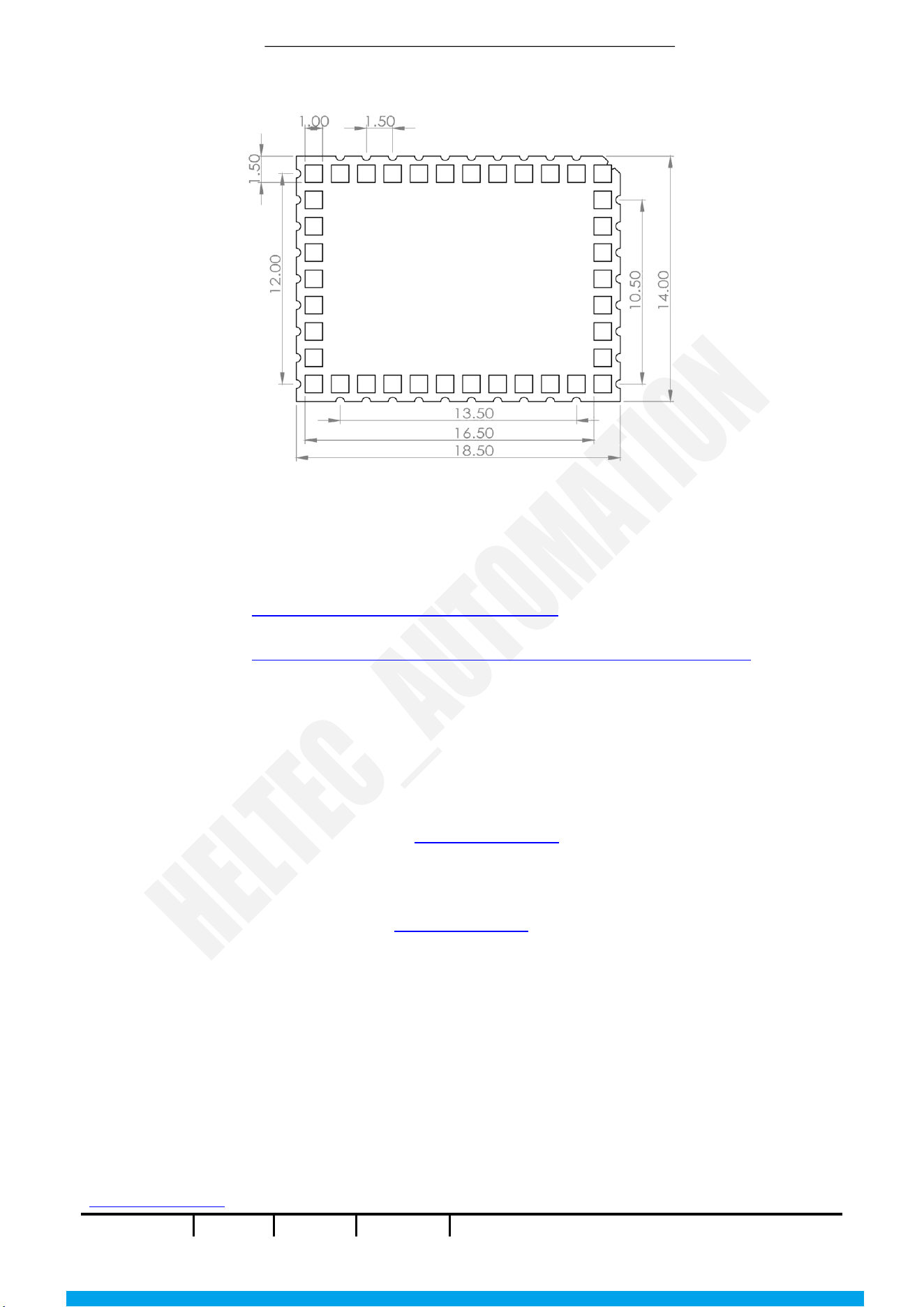
5.2 PCB footprint
For a detailed PCB Footprint, please refer to the following link:
https://resource.heltec.cn/download/Heltec_Module_Footprint/HT-HC01
HELTEC/
AUTOMATION
AUTOMATION
/HELTEC
https://heltec.org
Documents
Rev. 1.0
P 16/23
May 2024
Heltec Automation © Limited standard files
6 Resource
6.1Relevant resources
Documents Page: Heltec Products Operation Documention
Reference Design: https://resource.heltec.cn/download/HT-HC01/Reference_design
6.2 Heltec Contact Information
Heltec Automation Technology Co., Ltd
Chengdu, Sichuan, China
Email: [email protected]
Phone: +86-028-62374838
https://heltec.org
FCC Statement
This device complies with part 15 of the FCC rules. Operation is subject to the
following two conditions: (1) this device may not cause harmful interference, and (2)
this device must accept any interference received, including interference that may
cause undesired operation.
HELTEC/
AUTOMATION
AUTOMATION
/HELTEC
https://heltec.org
Documents
Rev. 1.0
P 17/23
May 2024
Heltec Automation © Limited standard files
Changes or modifications not expressly approved by the party responsible for
compliance could void the user’s authority to operate the equipment.
NOTE: This equipment has been tested and found to comply with the limits for a Class
B digital device, pursuant to part 15 of the FCC Rules. These limits are designed to
provide reasonable protection against harmful interference in a residential
installation. This equipment generates, uses and can radiate radio frequency energy
and, if not installed and used in accordance with the instructions, may cause harmful
interference to radio communications. However, there is no guarantee that interference
will not occur in a particular installation. If this equipment does cause harmful
interference to radio or television reception, which can be determined by turning the
equipment off and on, the user is encouraged to try to correct the interference by
one or more of the following measures:
‐ Reorient or relocate the receiving antenna.
‐ Increase the separation between the equipment and receiver.
‐ Connect the equipment into an outlet on a circuit different from that to which the
receiver is connected.
‐ Consult the dealer or an experienced radio/TV technician for help
Important Note: Radiation Exposure Statement
This equipment complies with FCC radiation exposure limits set forth for an
uncontrolled environment. This equipment should be installed and operated with minimum
distance 20cm between the radiator and your body.
This transmitter must not be co-located or operating in conjunction with any other
antenna or transmitter. Country Code selection feature to be disabled for products
marketed to the US/Canada.
HELTEC/
AUTOMATION
AUTOMATION
/HELTEC
https://heltec.org
Documents
Rev. 1.0
P 18/23
May 2024
Heltec Automation © Limited standard files
This device is intended only for OEM integrators under the following conditions:
1. The antenna must be installed such that 20 cm is maintained between the antenna
and users;
2. The transmitter module may not be co-located with any other transmitter or antenna;
3. For all products marketed in US, OEM has to limit the operation channels in CH1
to CH11 for 2.4G band by supplied firmware programming tool. OEM shall not supply any
tool or info to the end-user regarding to Regulatory Domain change. (If modular, only
test Channel 1-11)
As long as the three conditions above are met, further transmitter testing will not
be required. However, the OEM integrator is still responsible for testing their
end-product for any additional compliance requirements required with this module
installed.
Important Note:
In the event that these conditions cannot be met (for example certain laptop
configurations or co-location with another transmitter), then the FCC authorization
is no longer considered valid and the FCC ID cannot be used on the final product. In
these circumstances, the OEM integrator will be responsible for re-evaluating the end
product (including the transmitter) and obtaining a separate FCC authorization.
End Product Labeling
The final end product must be labeled in a visible area with the following: Contains
FCC ID: 2A2GJ-HT-HC01
Manual Information to the End User
HELTEC/
AUTOMATION
AUTOMATION
/HELTEC
https://heltec.org
Documents
Rev. 1.0
P 19/23
May 2024
Heltec Automation © Limited standard files
The OEM integrator has to be aware not to provide information to the end user regarding
how to install or remove this RF module in the user’s manual of the end product which
integrates this module.
The end user manual shall include all required regulatory information/warning as show
in this manual.
Integration instructions for host product manufacturers according to KDB 996369 D03
OEM Manual v01r01
2.2 List of applicable FCC rules
CFR 47 FCC PART 15 SUBPART C and CFR 47 FCC PART 15 SUBPART E has been investigated.
It is applicable to the modular transmitter.
2.3 Specific operational use conditions
This module is stand-alone modular. If the end product will involve the Multiple
simultaneously transmitting condition or different operational conditions for a
stand-alone modular transmitter in a host, host manufacturer have to consult with
module manufacturer for the installation method in end system.
This radio transmitter 2A2GJ-HT-HC01 has been approved by Federal Communications
Commission to operate with the antenna types listed below, with the maximum permissible
gain indicated. Antenna types not included in this list that have a gain greater than
the maximum gain indicated for any type listed are strictly prohibited for use with
this device. The concrete contents to check are the following three points.
1) Must use an antenna such as Dipole Antenna with a gain not exceeding 5.5 dBi;
2) Should be installed so that the end user cannot modify the antenna;
HELTEC/
AUTOMATION
AUTOMATION
/HELTEC
https://heltec.org
Documents
Rev. 1.0
P 20/23
May 2024
Heltec Automation © Limited standard files
3) Feed line should be designed in 50ohm.
Fine-tuning of return loss etc. can be performed using a matching network. The antenna
shall not be accessible for modification or change by the end user. A modification
to the antenna requires FCC/ISED Class II permissive change.
This device has been approved as mobile device in accordance with FCC and ISED Canada
RF exposure requirements. This means that a restricted minimum separation distance
of 20cm between the antenna and any person is mandatory.
A change in use that involves a separation distance ≤20cm (Portable usage) between
the Module’s antenna and any persons is a change in the RF exposure of the module
and, hence, is subject to a FCC Class 2 Permissive Change and a ISED Canada Class 4
Permissive Change policy in accordance with FCC KDB 996396 D01 and ISED Canada RSP-100.
2.4 Limited module procedures
Not applicable
2.5 Trace antenna designs
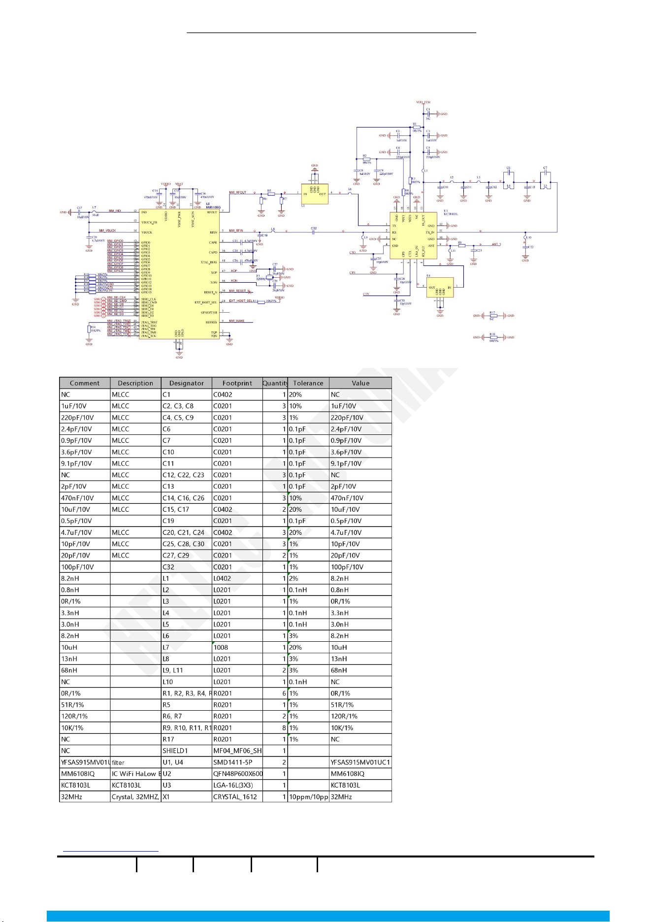
The antenna circuit adopts standard 50Ω impedance matching design, with complete
trace layout and supporting electronic components between the module RF output
terminal and antenna terminal. The detailed antenna circuit trace information and
supporting component parameters are listed in the table below:
HELTEC/
AUTOMATION
AUTOMATION
/HELTEC
https://heltec.org
Documents
Rev. 1.0
P 22/23
May 2024
Heltec Automation © Limited standard files
2.6 RF exposure considerations
This equipment complies with FCC radiation exposure limits set forth for an
uncontrolled environment. This equipment should be installed and operated with minimum
distance 20cm between the radiator & your body.
2.7 Antennas
This radio transmitter FCC ID: 2A2GJ-HT-HC01 has been approved by Federal
Communications Commission to operate with the antenna types listed below, with the
maximum permissible gain indicated. Antenna types not included in this list that have
a gain greater than the maximum gain indicated for any type listed are strictly
prohibited for use with this device.
Max. Antenna Gain & Antenna Type: 2.5dBi Dipole Antenna
2.8 Label and compliance information
The final end product must be labeled in a visible area with the following: Contains
FCC ID: 2A2GJ-HT-HC01
2.9 Information on test modes and additional testing requirements
Host manufacturer which installs this modular with single modular approval shall
perform the test of radiated emission and spurious emission according to FCC part
15C:15.247 and FCC Part 15 and 15.209 requirements. Only if the test results comply
with the above standards can the host product be sold legally.
2.10 Additional testing, Part 15 Subpart B disclaimer
HELTEC/
AUTOMATION
AUTOMATION
/HELTEC
https://heltec.org
Documents
Rev. 1.0
P 23/23
May 2024
Heltec Automation © Limited standard files
Host manufacturer is responsible for compliance of the host system with module
installed with all other applicable requirements for the system such as Part 15 B.
2.11 Note EMI Considerations
Host manufacture is recommended to use D04 Module Integration Guide recommending as
"best practice" RF design engineering testing and evaluation in case non-linear
interactions generate additional non-compliant limits due to module placement to host
components or properties.
2.12 How to make changes
This module is stand-alone modular. If the end product will involve the Multiple
simultaneously transmitting condition or different operational conditions for a
stand-alone modular transmitter in a host, host manufacturer have to consult with
module manufacturer for the installation method in end system. According to the KDB
996369 D02 Q&A Q12, a host manufacture only needs to do an evaluation (i.e., no C2PC
required when no emission exceeds the limit of any individual device (including
unintentional radiators) as a composite). The host manufacturer must fix any failure.