1. IntroductiontoP401-DAI
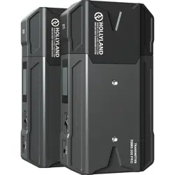
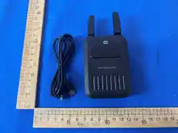
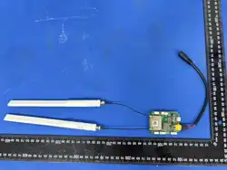
P401-DAIisa2.4/5.8Gdual-band,high-bandwidth,high-power,2x2MIMOwirelessdata
transmissionmodule.BasedontheprincipleofTDD,ituseskeytechnologiessuchasOFDMand
MIMOtoimprovefrequencybandutilizationwhileprovidingalongertransmissiondistance.It
supportsautomaticfrequencyhoppingandautonomousdynamicadjustmentofMCS,andhas
advantagessuchaslongrange,stronganti-interferenceability,andlowlatency.Asahighly
integratedmoduleproduct,thisproductcanbewidelyusedinfieldssuchasdrones,security
monitoring,wirelessscreenprojection,wirelessaudioandvideo,andspecialinspections,and
canmeettheneedsofcustomersforrapiddevelopmentandapplication.
P401-DAIcanoperateinAPandDevicemodes,enablingstableandreliablelong-range
wirelesscommunication.
2. TechnicalFeaturesofP401-DAIModule
•
BasedontheprincipleofTDD,keytechnologiessuchasOFDMandMIMOareadoptedto
improvetheutilizationoffrequencybands.
•
SupportsAESencryption,multiplesecuritypolicies,andpreventsillegaleavesdroppingand
interception.
•
Adoptafrequencyhoppingscheme,monitorinterferenceinrealtime,andautomatically
selectthefrequencyhoppingrange;basedontheinterferencesituationofthecurrent
channel,automaticallyandquicklychangethefrequencypointandadjusttheModulation
andCodingScheme(MCS).
•
Supportsstarnetworkingplusrelaynetworking,enablingtheconstructionofwirelessmulti-
hopnetworkingapplications.
•
Themaximumrateofairinterfacetransmissioncanreach40Mbps.
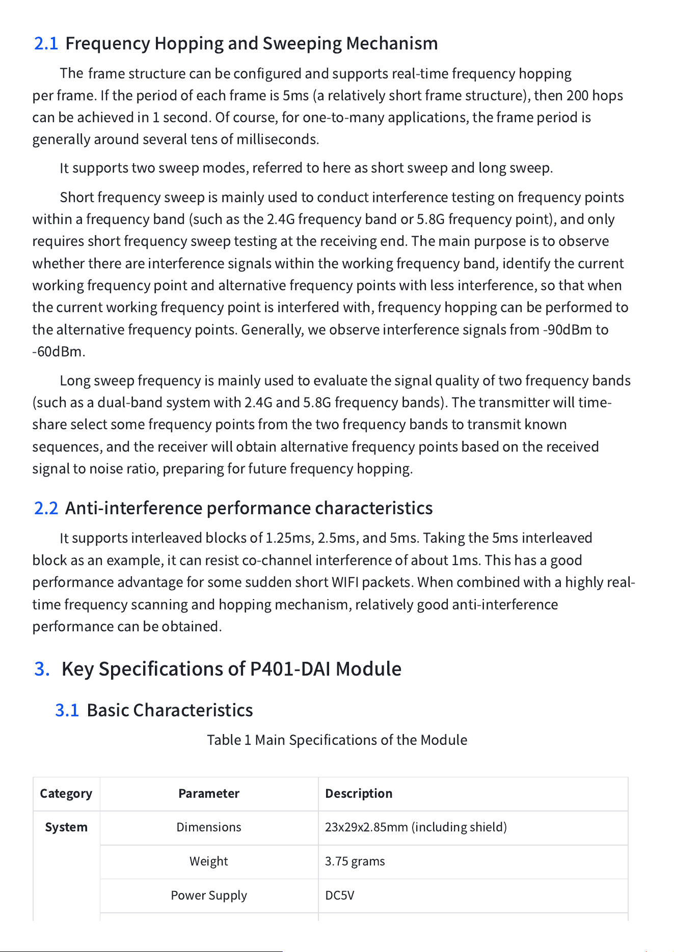
2.1 FrequencyHoppingandSweepingMechanism
The
framestructurecanbeconfiguredandsupportsreal-timefrequencyhopping
perframe.Iftheperiodofeachframeis5ms(arelativelyshortframestructure),then200hops
canbeachievedin1second.Ofcourse,forone-to-manyapplications,theframeperiodis
generallyaroundseveraltensofmilliseconds.
It
supportstwosweepmodes,referredtohereasshortsweepandlongsweep.
Shortfrequencysweepismainlyusedtoconductinterferencetestingonfrequencypoints
withinafrequencyband(suchasthe2.4Gfrequencybandor5.8Gfrequencypoint),andonly
requiresshortfrequencysweeptestingatthereceivingend.Themainpurposeistoobserve
whetherthereareinterferencesignalswithintheworkingfrequencyband,identifythecurrent
workingfrequencypointandalternativefrequencypointswithlessinterference,sothatwhen
thecurrentworkingfrequencypointisinterferedwith,frequencyhoppingcanbeperformedto
thealternativefrequencypoints.Generally,weobserveinterferencesignalsfrom-90dBmto
-60dBm.
Longsweepfrequencyismainlyusedtoevaluatethesignalqualityoftwofrequencybands
(suchasadual-bandsystemwith2.4Gand5.8Gfrequencybands).Thetransmitterwilltime-
shareselectsomefrequencypointsfromthetwofrequencybandstotransmitknown
sequences,andthereceiverwillobtainalternativefrequencypointsbasedonthereceived
signaltonoiseratio,preparingforfuturefrequencyhopping.
2.2 Anti-interferenceperformancecharacteristics
It
supportsinterleavedblocksof1.25ms,2.5ms,and5ms.Takingthe5msinterleaved
blockasanexample,itcanresistco-channelinterferenceofabout1ms.Thishasagood
performanceadvantageforsomesuddenshortWIFIpackets.Whencombinedwithahighlyreal-
timefrequencyscanningandhoppingmechanism,relativelygoodanti-interference
performancecanbeobtained.
3. KeySpecificationsofP401-DAIModule
3.1 BasicCharacteristics
Table1MainSpecificationsoftheModule
Category
Parameter
Description
System
Dimensions 23x29x2.85mm(includingshield)
Weight 3.75grams
PowerSupply DC5V
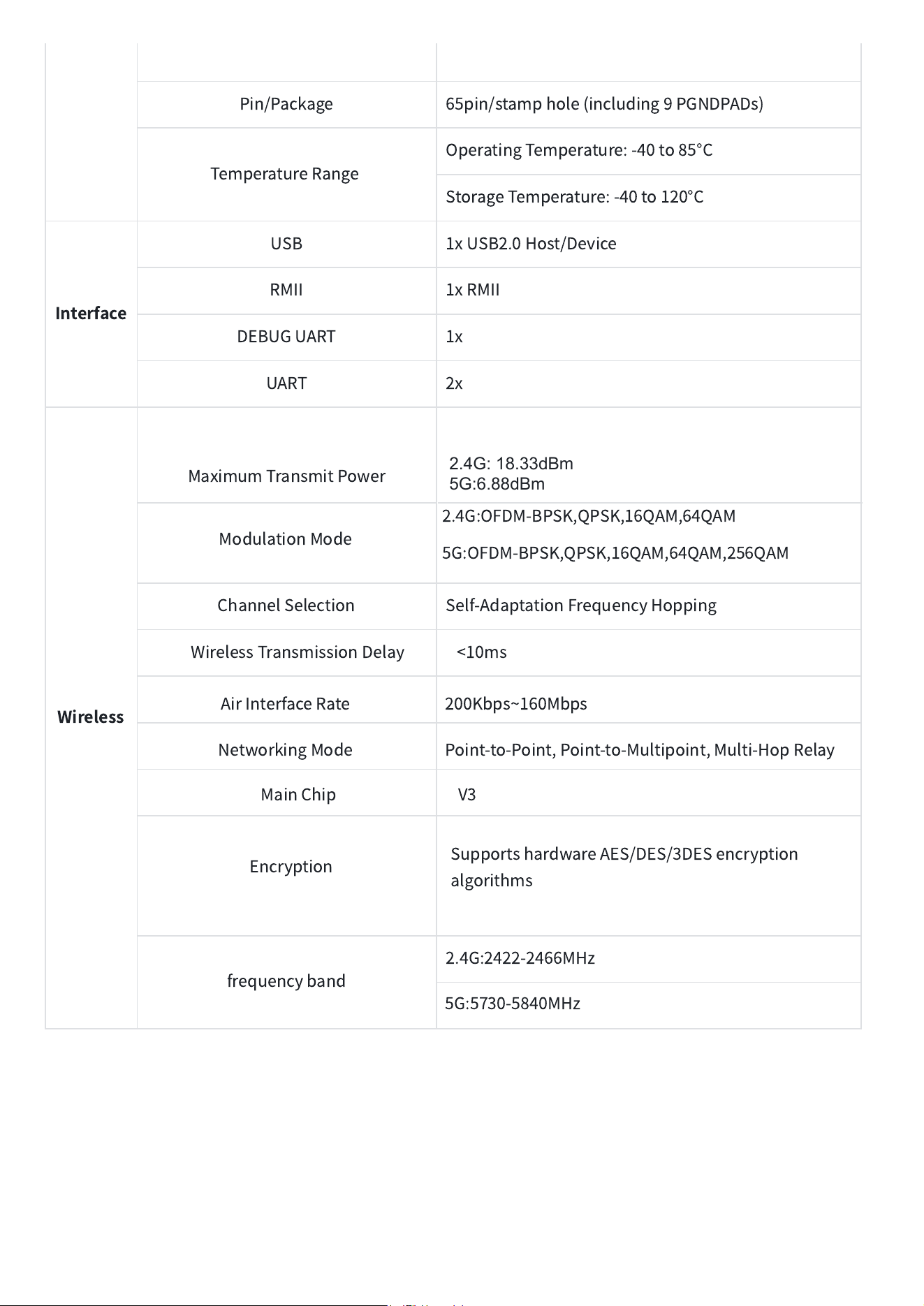
Pin/Package 65pin/stamphole(including9PGNDPADs)
TemperatureRange
OperatingTemperature:-40to85°C
StorageTemperature:-40to120°C
Interface
USB 1xUSB2.0Host/Device
RMII 1xRMII
DEBUGUART 1x
UART 2x
Wireless
MaximumTransmitPower
ModulationMode
ChannelSelection Self-AdaptationFrequencyHopping
WirelessTransmissionDelay <10ms
AirInterfaceRate 200Kbps~160Mbps
NetworkingMode Point-to-Point,Point-to-Multipoint,Multi-HopRelay
MainChip V3
Encryption
SupportshardwareAES/DES/3DESencryption
algorithms
frequencyband
2.4G:2422-2466MHz
2.4G:OFDM-BPSK,QPSK,16QAM,64QAM
5G:OFDM-BPSK,QPSK,16QAM,64QAM,256QAM
5G:5730-5840MHz
2.4G: 18.33dBm
5G:6.88dBm
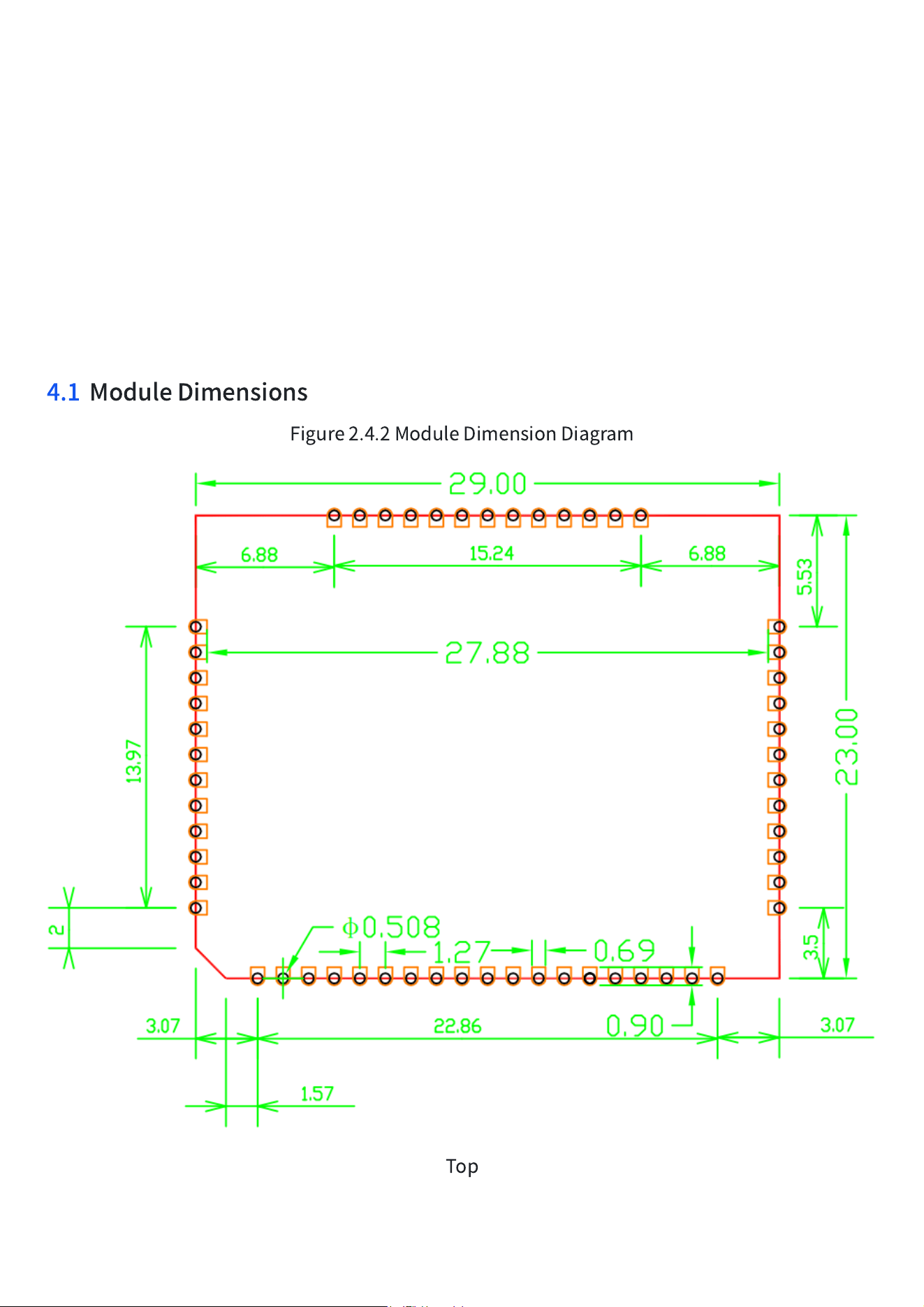
4.1 ModuleDimensions
Figure2.4.2ModuleDimensionDiagram
Top
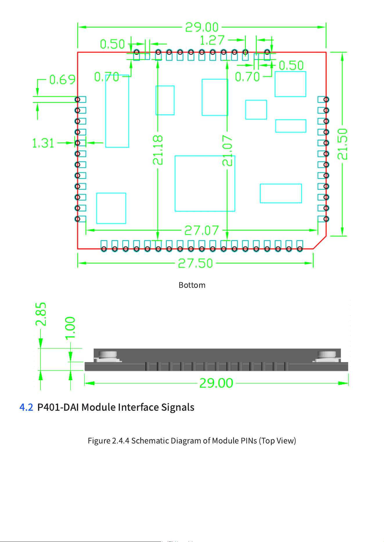
Bottom
4.2 P401-DAIModuleInterfaceSignals
Figure2.4.4SchematicDiagramofModulePINs(TopView)
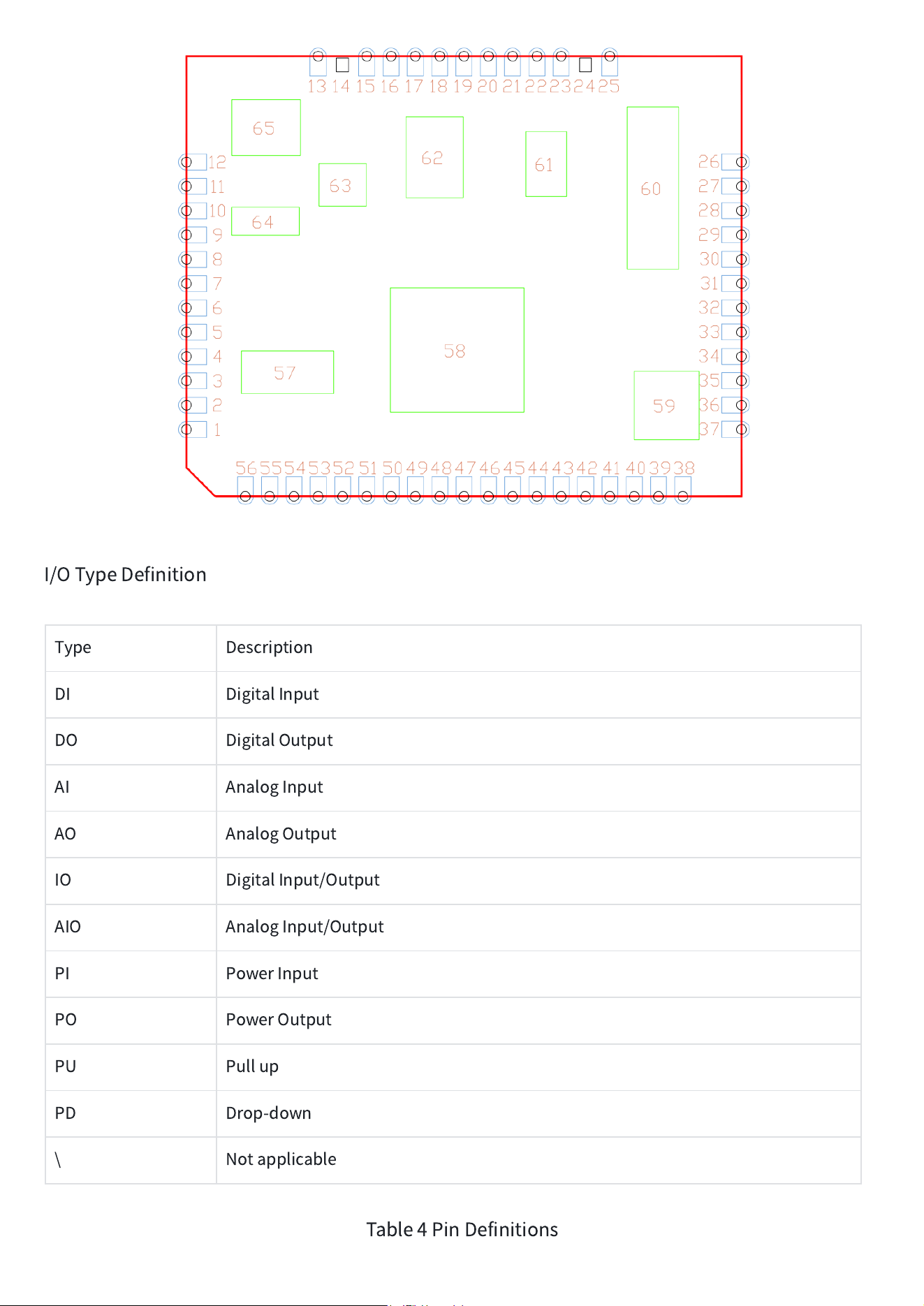
I/OTypeDefinition
Type Description
DI DigitalInput
DO DigitalOutput
AI AnalogInput
AO AnalogOutput
IO DigitalInput/Output
AIO AnalogInput/Output
PI PowerInput
PO PowerOutput
PU Pullup
PD Drop-down
\ Notapplicable
Table4PinDefinitions
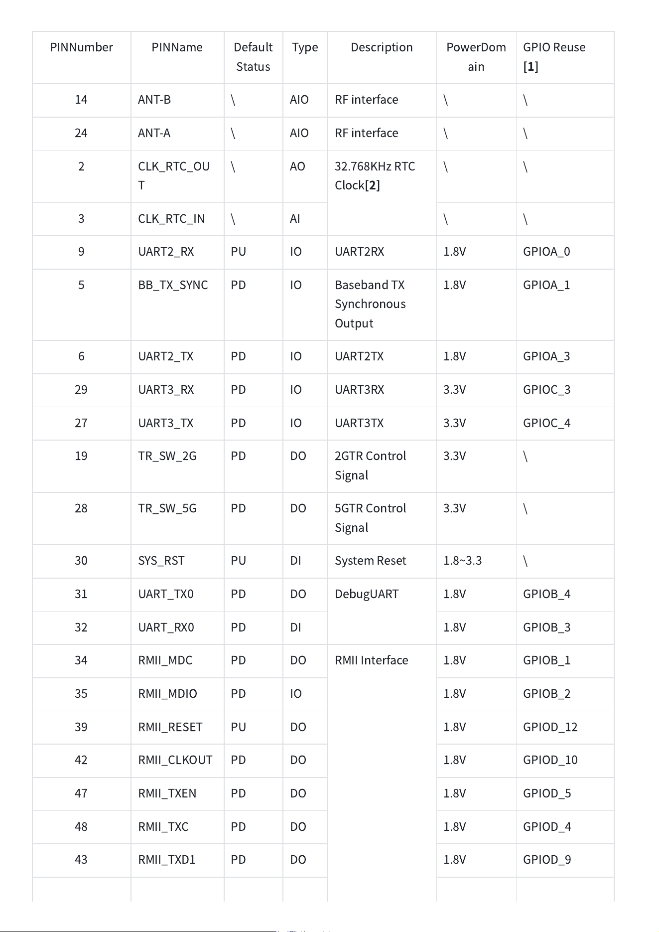
PINNumber PINName Default
Status
Type Description PowerDom
ain
GPIOReuse
[1]
14 ANT-B \ AIO RFinterface \ \
24 ANT-A \ AIO RFinterface \ \
2 CLK_RTC_OU
T
\ AO 32.768KHzRTC
Clock
[2]
\ \
3 CLK_RTC_IN \ AI \ \
9 UART2_RX PU IO UART2RX 1.8V GPIOA_0
5 BB_TX_SYNC PD IO BasebandTX
Synchronous
Output
1.8V GPIOA_1
6 UART2_TX PD IO UART2TX 1.8V GPIOA_3
29 UART3_RX PD IO UART3RX 3.3V GPIOC_3
27 UART3_TX PD IO UART3TX 3.3V GPIOC_4
19 TR_SW_2G PD DO 2GTRControl
Signal
3.3V \
28 TR_SW_5G PD DO 5GTRControl
Signal
3.3V \
30 SYS_RST PU DI SystemReset 1.8~3.3 \
31 UART_TX0 PD DO DebugUART 1.8V GPIOB_4
32 UART_RX0 PD DI 1.8V GPIOB_3
34 RMII_MDC PD DO RMIIInterface 1.8V GPIOB_1
35 RMII_MDIO PD IO 1.8V GPIOB_2
39 RMII_RESET PU DO 1.8V GPIOD_12
42 RMII_CLKOUT PD DO 1.8V GPIOD_10
47 RMII_TXEN PD DO 1.8V GPIOD_5
48 RMII_TXC PD DO 1.8V GPIOD_4
43 RMII_TXD1 PD DO 1.8V GPIOD_9
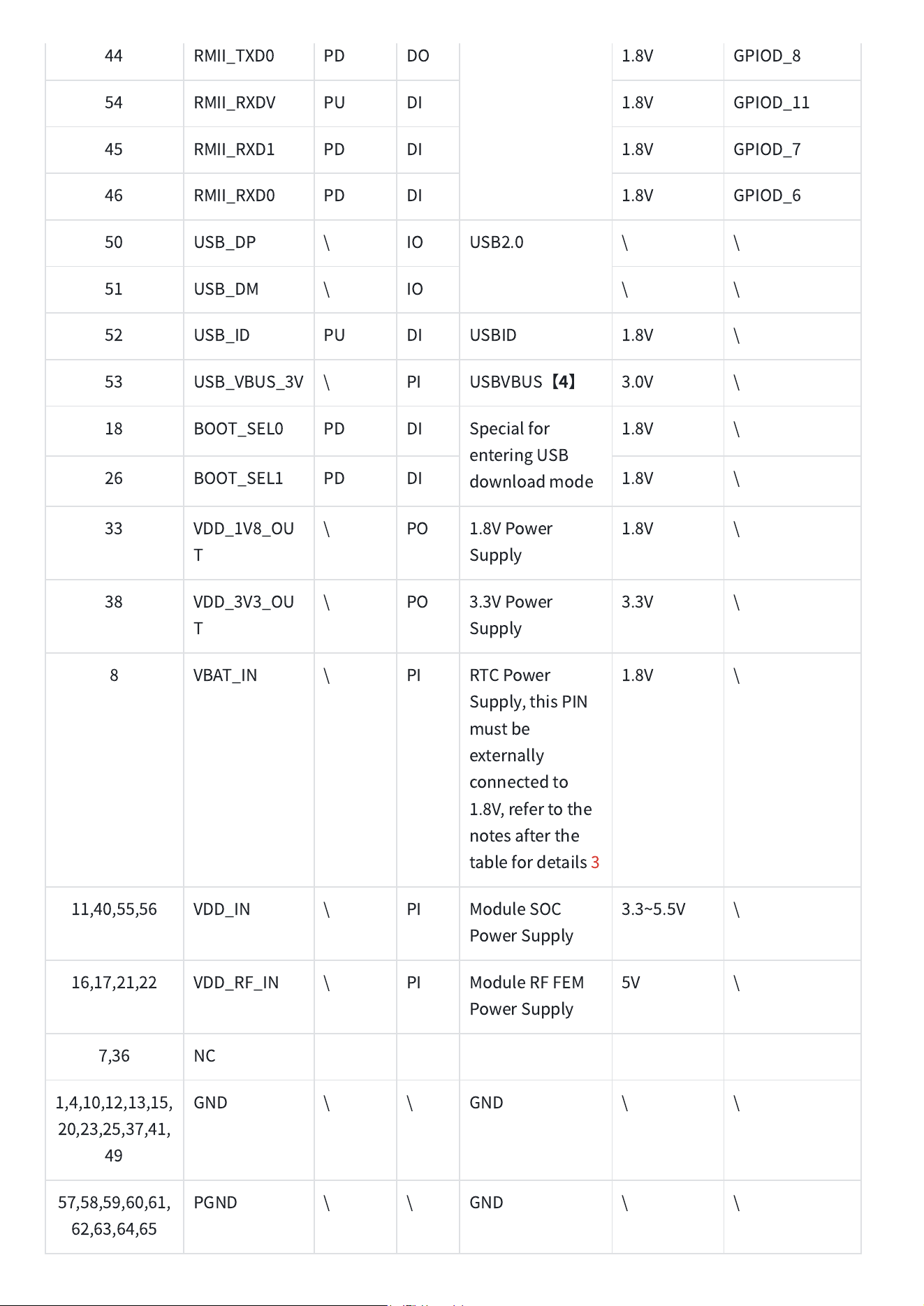
44 RMII_TXD0 PD DO 1.8V GPIOD_8
54 RMII_RXDV PU DI 1.8V GPIOD_11
45 RMII_RXD1 PD DI 1.8V GPIOD_7
46 RMII_RXD0 PD DI 1.8V GPIOD_6
50 USB_DP \ IO USB2.0 \ \
51 USB_DM \ IO \ \
52 USB_ID PU DI USBID 1.8V \
53 USB_VBUS_3V \ PI USBVBUS
【
4
】
3.0V \
18 BOOT_SEL0 PD DI Specialfor
enteringUSB
downloadmode
1.8V \
26 BOOT_SEL1 PD DI 1.8V \
33 VDD_1V8_OU
T
\ PO 1.8VPower
Supply
1.8V \
38 VDD_3V3_OU
T
\ PO 3.3VPower
Supply
3.3V \
8 VBAT_IN \ PI RTCPower
Supply,thisPIN
mustbe
externally
connectedto
1.8V,refertothe
notesafterthe
tablefordetails3
1.8V \
11,40,55,56 VDD_IN \ PI ModuleSOC
PowerSupply
3.3~5.5V \
16,17,21,22 VDD_RF_IN \ PI ModuleRFFEM
PowerSupply
5V \
7,36 NC
1,4,10,12,13,15,
20,23,25,37,41,
49
GND \ \ GND \ \
57,58,59,60,61,
62,63,64,65
PGND \ \ GND \ \

Federal Communications Commission (FCC) Statement
This device complies with part 15 of the FCC Rules. Operation is subject to the following
two conditions:
(1) This device may not cause harmful interference, and
(2) this device must accept any interference received, including interference that may
cause undesired operation
Note:This equipment has been tested and found to comply with the limits for a Class B
digital device, pursuant to part 15 of the FCC Rules. These limits are designed to provide
Reasonable protection against harmful interference in a residential installation. This
equipment generates, uses and can radiate radio frequency energy and, if not installed
and used in accordance with the instructions, may cause harmful interference to radio
communications. However, there is no guarantee that interference will not occur in a
particular installation. If this equipment does cause harmful interference to radio or
television reception, which can be determined by turning the equipment off and on, the
user is encouraged to try to correct the interference by one or more of the following
measures: Reorient or relocate the receiving antenna.
. Increase the separation between the equipment and receiver.
. Connect the equipment into an outlet on a circuit different from that to which
the receiver is connected.
. Consult the dealer or an experienced radio/TV technician for help.
Warning: Any changes or modifications not expressly approved by the party responsible
for compliance could void the user's authority to operate the equipment.
RF exposure statement:
This equipment complies with FCC radiation exposure limits set forth for an uncontrolled
environment. This equipment should be installed and operated with minimum distance
20cm between the radiator&your body.

OEM Guidance
1. Applicable FCC rules
This module has been tested and found to comply with part 15.247 and requirements for
Modular Approval.
2. The specific operational use conditions
This module can be used in IoT devices. The input voltage to the module is nominally
V
DC. The
operational ambient temperature of the module is - to degree C. Only the authorized
antenna is allowed. Any other external antenna is prohibited.
3. Limited module procedures
N/A
4. Trace antenna design
N/A
5. RF exposure considerations
This equipment complies with FCC radiation exposure limits set forth for an uncontrolled environment.
This equipment should be installed and operated with minimum distance 20cm between the radiator&
40
5
85
part 15.407
your body.
M onopole

6. Antenna
Antenna type: PCB antenna; Peak gain: 3.40dBi
7. Label and compliance information
An exterior label on
OEM’s end product can use wording such as the following:
“Contains Transmitter Module FCC ID: 2AC7Z-ESP32WROOM32E” or
“Contains FCC ID: 2AC7Z-ESP32WROOM32E.”
6. Antenna
Antenna type :
; Antenna Max. Peak Gain
7. La
bel and compliance information
can be used only when all FCC ID compliance requirements are met.
8. Information on test modes and additional testing requirements
a)The modular transmitter has been fully tested by the module grantee on the required
number of channels,modulation types, and modes, it should not be necessary for the host
installer to re-test all the available transmitter modes or settings. It is recommended that the
host product manufacturer, installing the modular transmitter,perform some investigative
measurements to confirm that the resulting composite system does not exceed the spurious
emissions limits or band edge limits (e.g., where a different antenna may be causing
additional emissions).
b)The testing should check for emissions that may occur due to the intermixing of emissions
with the other transmitters, digital circuitry, or due to physical properties of the host product
(enclosure). This investigation is especially important when integrating multiple modular
transmitters where the certification is based on testing each of them in a stand-alone
configuration. It is important to note that host product manufacturers should not assume that
because the modular transmitter is certified that they do not have any responsibility for final
product compliance.
c)
If the investigation indicates a compliance concern the host product manufacturer is
obligated to mitigate the issue. Host products using a modular transmitter are subject to all
the applicable individual technical rules as well as to the general conditions of operation in
Sections 15.5, 15.15, and 15.29 to not cause interference. The operator of the host product
will be obligated to stop operating the device until the interference have been corrected .
The FCC ID
When the module is installed in the host device, the FCC ID label must be visible through a
window on the final device or it must be visible when an access panel, door or cover is easily
re-moved. If not, a second label must be placed on the outside of the final device that
contains the following text: “Contains FCC ID:
9. Additional testing, Part 15 Subpart B disclaimer
The final host / module combination need to be evaluated against the FCC Part 15B criteria for
unintentional radiators in order to be properly authorized for operation as a Part15 digital device.
The host integrator installing this module into their product must ensure that the final composite
product complies with the FCC requirements by a technical assessment or evaluation to the FCC
rules,including the transmitter operation and should refer to guidance in KDB 996369. For host
products with certified modular transmitter, the frequency range of investigation of the composite
system is specified by rule in Sections 15.33(a)(1) through (a)(3), or the range applicable to the
digital device, as shown in Section 15.33(b)(1), whichever is the higher frequency range of
investigation. When testing the host product, all the transmitters must be operating. The transmitters
can be enabled by using publiclyavailable drivers and turned on, so the transmitters are active. In
certain conditions it might be appropriate to use a technology-specific call box (test set) where
accessory devices or drivers are not available. When testing for emissions from the unintentional
radiator, the transmitter shall be placed in the receive mode or idle mode, if possible. If receive mode
only is not possible then, the radio shall be passive (preferred) and/or active scanning. In these
cases, this would need to enable activity on the communication BUS (i.e., PCIe, SDIO, USB) to
ensure the unintentional radiator circuitry is enabled.
Testing laboratories may need to add attenuation or filters depending on the signal strength of any
active beacons (if applicable) from the enabled radio(s). See ANSI C63.4, ANSI C63.10 for
further general testing details.
2BVSJP401-DAI
Monopole Antenna
:2.4G:3.38dBi,5G:5.52dBi