
BL-M8852BP2
802.11ax 1200Mbps WLAN + BT v5.2
PCI-E Module Specification
SHENZHEN BILIAN ELECTRONIC CO., LTD
Add: 10~11/F, Building 1A, Huaqiang idea park, Guangming district, Shenzhen. Guangdong, China
Web: www.b-link.net.cn
1 http://www.b-link.net.cn
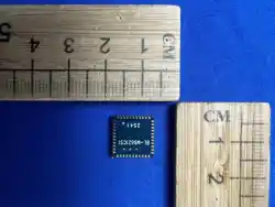
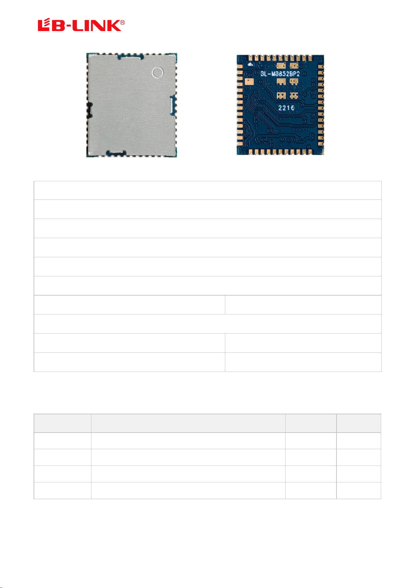
(Top View) (Bottom View)
Module Name: BL-M8852BP2
Module Type: 802.11a/b/g/n/ac/ax 1200Mbps WLAN + Bluetooth v5.2 Combo PCI-E Module
Revision: V1.1.1
Customer Approval:
Company:
Title:
Signature:
Date:
Approval:
Title:
Signature:
Date:
Revision History
Revision
Summary
Release Date
Revised By
1.1.0
Initial release
2026-01-21
Zjh
1.1.1
Official version
2026-02-26
Zjh
2 http://www.b-link.net.cn
1. Introduction
BL-M8852BP2 is a highly integrated Dual-band WLAN+Bluetooth Combo module. It combines a
2T2R Dual-band WLAN subsystem with PCI Express interface controllers and a Bluetooth v5.2
subsystem with UART interface controller. The module compatible IEEE 802.11a/b/g/n/ac/ax
standard and provides the maximum PHY rate up to 1201Mbps, it supports Bluetooth dual mode
with v5.2/v4.2/v2.1 compliant. The module provides a complete solution for high-performance
integrated WALN and Bluetooth devices such as OTT Boxes, Set-top Boxes, HD Cameras, etc.
1.1 Features
Operating Frequencies: 2.4~2.4835GHz or 5.15~5.85GHz
Support Dual-band 2T2R mode with 20/40/80Mhz bandwidth
Support 802.11ax with OFDMA and MU-MIMO
Dual Mode Bluetooth support : Simultaneous LE and BR / EDR
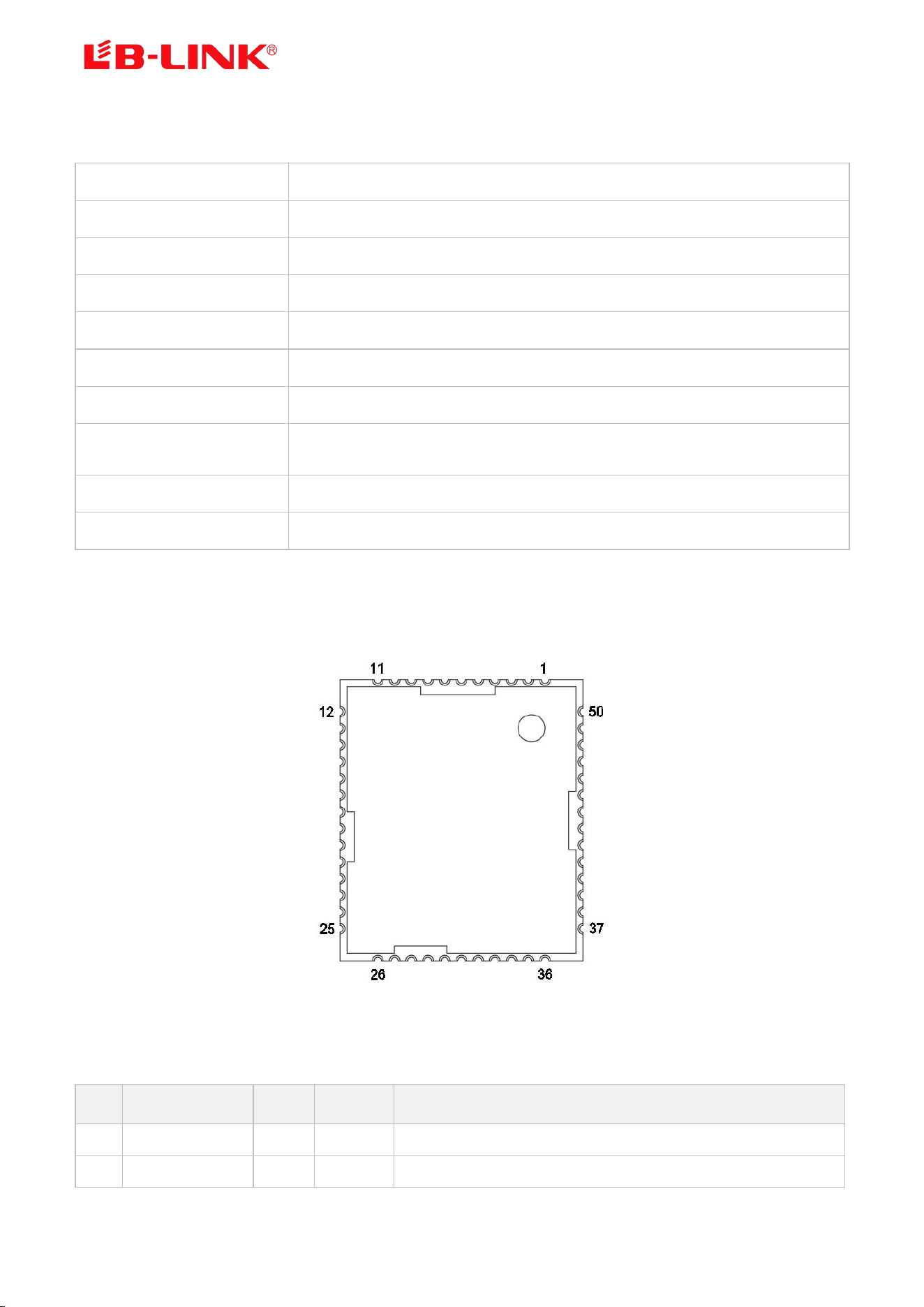
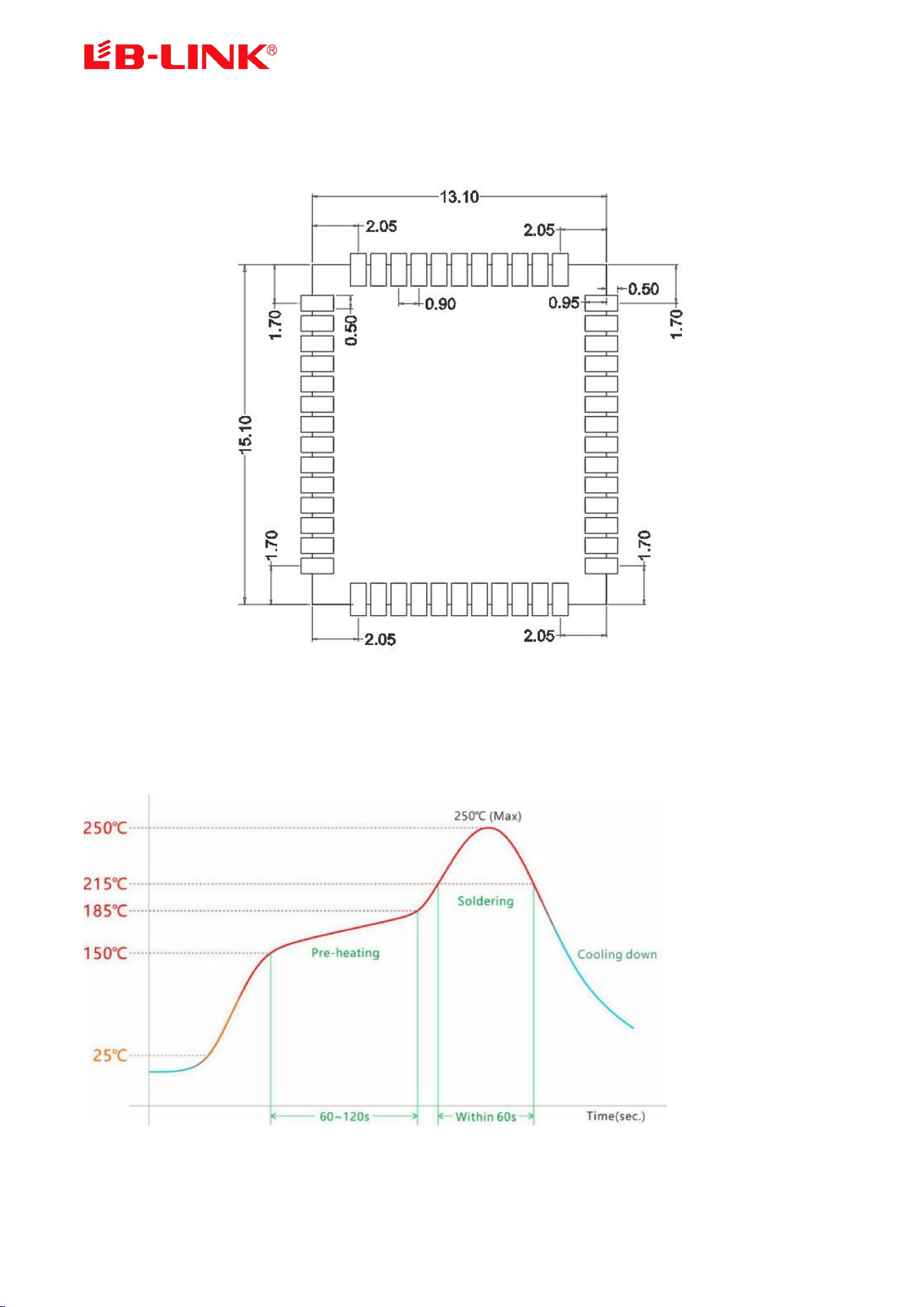
1.2 Block Diagram
3 http://www.b-link.net.cn
1.3 General Specifications
Module Name
BL-M8852BP2
Chipset
RTL8852BE-VR-CG
WLAN Standards
IEEE802.11a/b/g/n/ac/ax
BT Specification
Bluetooth Core Specification v5.2/4.2/2.1
Host Interface
PCI Express 2.1 for WLAN & UART for Bluetooth
Antenna
Connect to the external antennas through half hole pad
Dimension
15.1*13.1*2.2mm (L*W*H)
Power Supply
VDD33=3.3V±0.2V@1200 mA (Max)
VDDIO=3.3V±0.2V / 1.8V±0.1V
Operation Temperature
-20℃ to +70℃
Operation Humidity
10% to 95% RH (Non-Condensing)
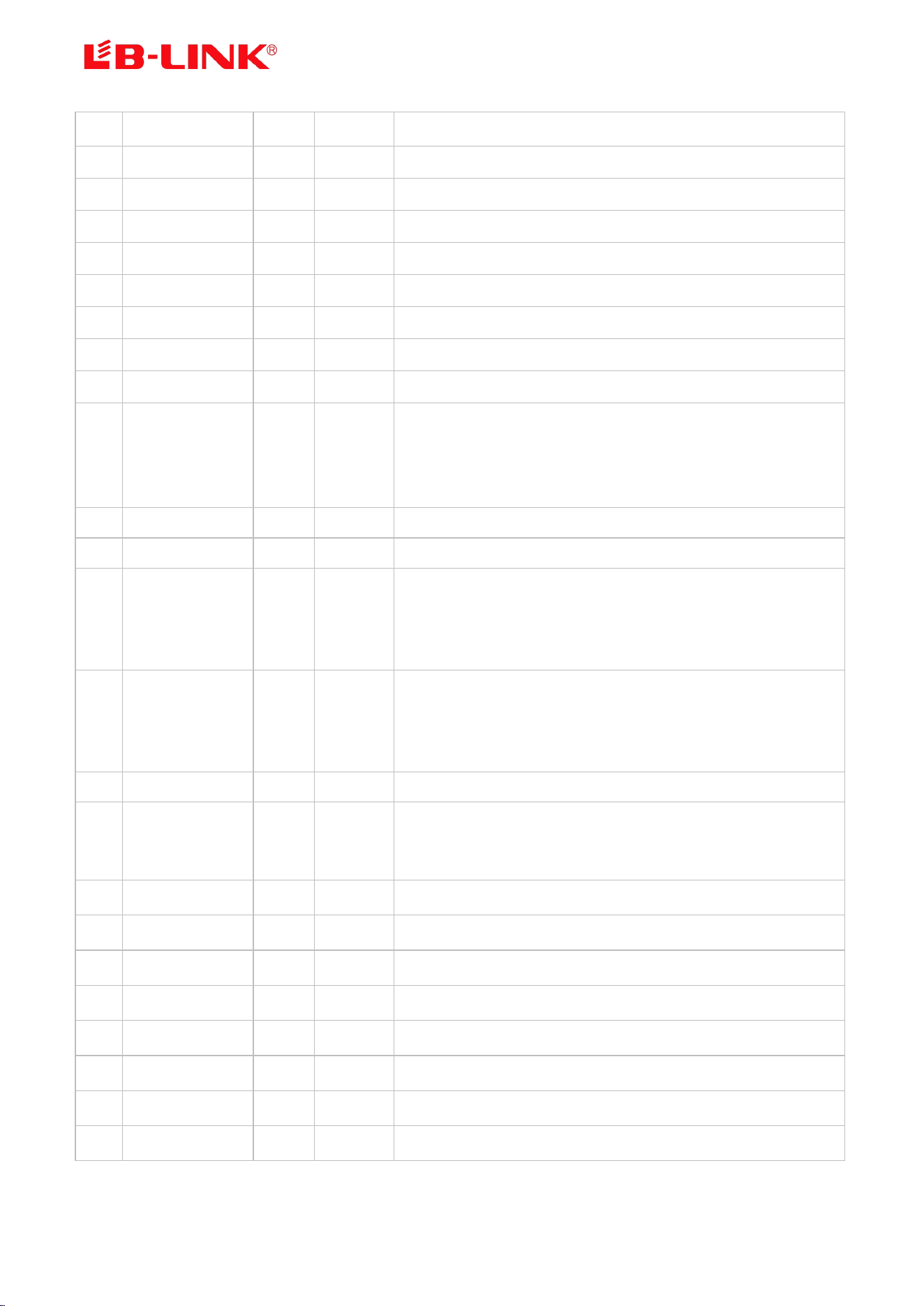
2. Pin Assignments
(Top View)
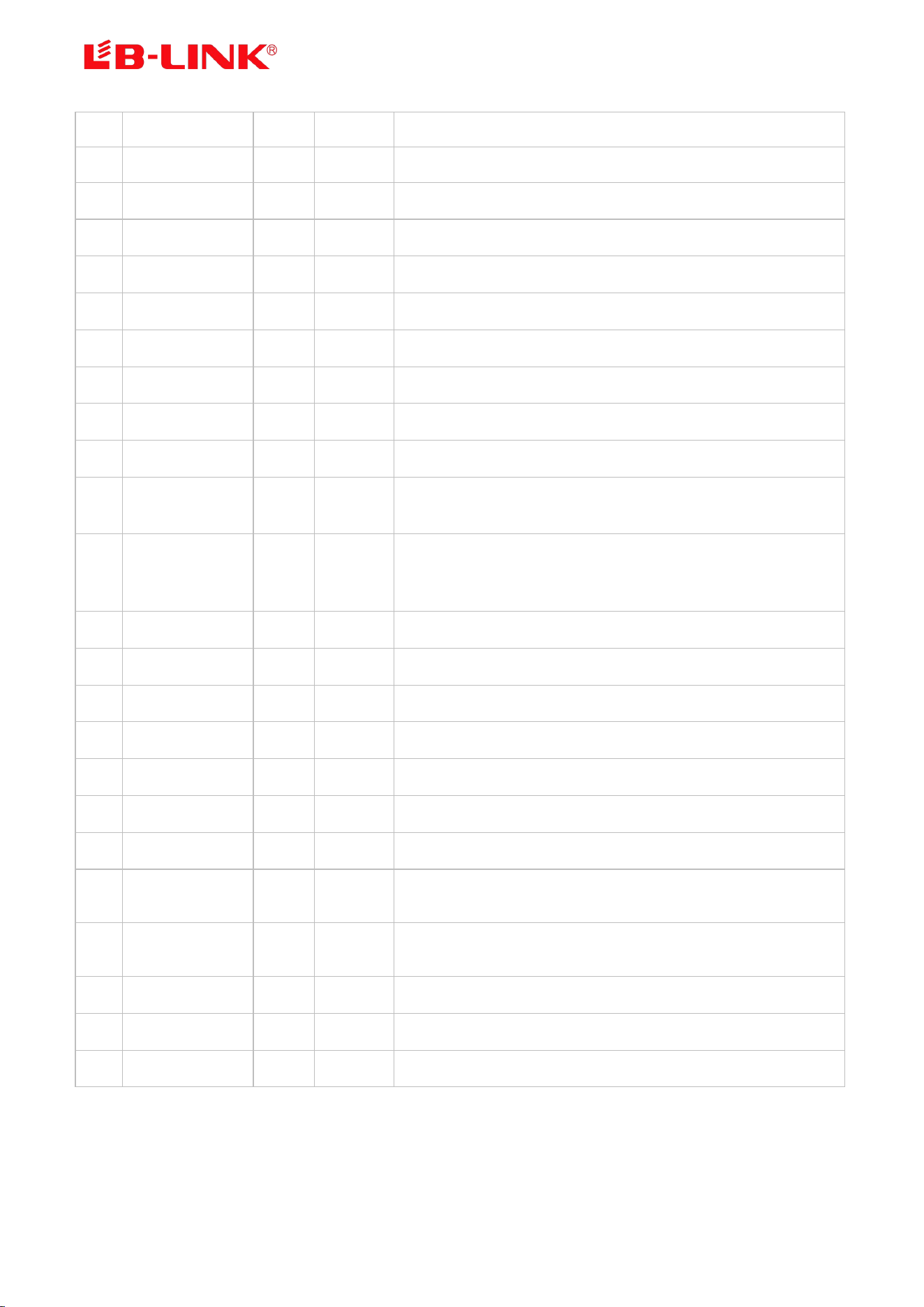
2.1 Pin Definition
No
Pin Name
Type
I/O Level
Module Pin Description
1
GND
RF
RF Ground
2
WLAN ANT1
RF
RF Pad for 2.4G / 5G RF to WLAN_ANT1
4 http://www.b-link.net.cn
3
GND
RF
RF Ground
4
GND
RF
RF Ground
5
GND
RF
RF Ground
6
GND
RF
RF Ground
7
GND
RF
RF Ground
8
GND
RF
RF Ground
9
WLAN ANT0
RF
RF Pad for 2.4G / 5G RF to WLAN_ANT0
10
GND
RF
RF Ground
11
GND
RF
RF Ground
12
PERST#
I
VDD33
PCI Express Reset active low input. When the PERST# is asserted
at power-on state, the module returns to a pre-defined reset
state and is ready for initialization and configuration after the
de-assertion of the PERST#
13
NC
-
NC
14
NC
-
NC
15
WL_DIS#
I
VDDIO
WL_DIS# can be defined as the WLAN Radio-of function with
host interface remaining connected. When this pin is pulled
low, WLAN function will be Radio-off. Shared with GPI09. In
ternal pull High by 100K resistor
16
WAKE#
O/D
VDD33
Power Management Event active low open drain output. Use
d to reactivate the PCI Express bus main power rails and ref
erence clock. This WAKE# can be shared with BT wake up h
ost function via side band signals
17
NC
-
NC
18
HOST_WAKE_WL
I
VDDIO
The Host wakes up WLAN controller in remote Wake up Mo
de. Suggest configuring the control pin in platform side as o
pen-drain output. Shared with GPIO12
19
PCM_OUT
O
VDDIO
PCM data output. Shared with GPIO1
20
PCM_IN
I
VDDIO
PCM data input. Shared with GPIO0
21
PCM_SYNC
I/O
VDDIO
PCM Frame Sync signal. Shared with GPIO2
22
PCM_CLK
I/O
VDDIO
PCM Clock signal. Shared with GPIO3
23
GND
P
Ground
24
NC
-
NC
25
NC
-
NC
26
NC
-
NC
5 http://www.b-link.net.cn
27
GND
P
Ground
28
NC
-
NC
29
NC
-
NC
30
GND
P
Ground
31
NC
-
NC
32
GND
P
Ground
33
REFCLKn
AI
PCI Express 100MHz differential reference clock input
34
VDDIO
P
Power supply for some digital IO, 3.3V or 1.8V
35
REFCLKp
AI
PCI Express 100MHz differential reference clock input
36
VDD33
P
DC 3.3V power supply
37
CLKREQ#
O/D
VDD33
Reference Clock Request open drain output, it used to request for
the the reference clock. It also used by L1 PM substates
38
BT_DIS#
I
VDDIO
BT_DIS# can externally shut down the module BT function when
its pulled Low, and UART interface will be also disabled. Shared
with GPIO11. Internal pull High by 100K resistor
39
GND
P
Ground
40
UART_TX
O
VDDIO
High-speed UART data output
41
UART_RX
I
VDDIO
High-speed UART data input
42
UART_RTS
O
VDDIO
High-speed UART RTS output
43
UART_CTS
I
VDDIO
High-speed UART CTS input
44
PERn
AI
PCI Express device receive differential pair for WLAN
45
PERp
AI
PCI Express device receive differential pair for WLAN
46
PETn
AO
PCI Express device transmit differential pair for WLAN ( AC
coupling capacitors are integrated on module )
47
PETp
AO
PCI Express device transmit differential pair for WLAN ( AC
coupling capacitors are integrated on module )
48
BT_ANT
RF
RF Pad for BT RF to BT_ANT
49
HOST_WAKE_BT
I
VDDIO
The Host wakes up BT controller. Shared with GPIO7
50
BT_WAKE_HOST
O
VDDIO
BT to wake up the Host. Shared with GPIO14
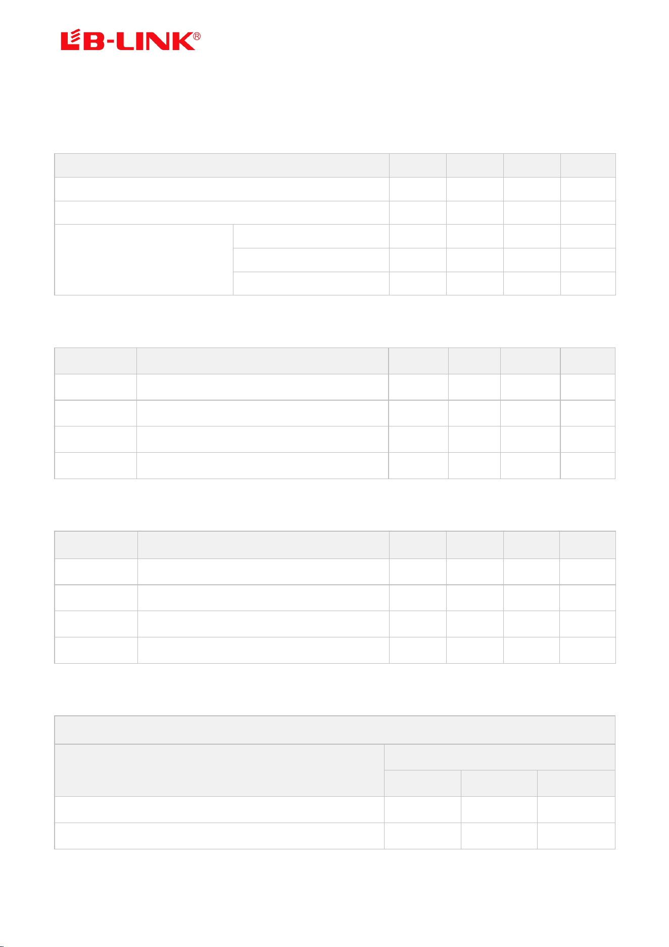
P: Power or Ground; I/O: digital In/Output; O/D:Open Drain digital Output;
AI/O: Analog In/Output; RF: Analog RF Port or RF Ground;
6 http://www.b-link.net.cn
3. Electrical and Thermal Specifications
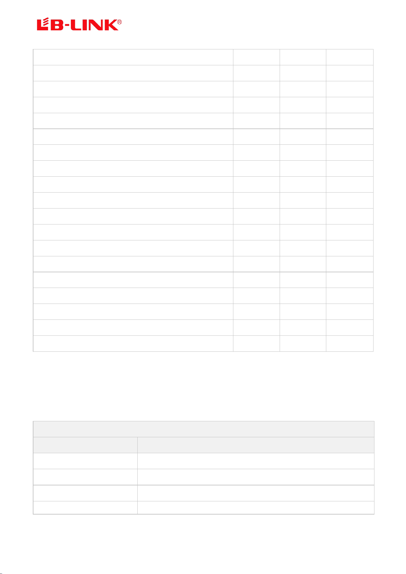
3.1 Recommended Operating Conditions
Parameters
Min
Typ
Max
Units
Ambient Operating Temperature
-20
25
70
℃
External Antenna VSWR
1.7
2.1
Supply Voltage
VDD33
3.1
3.3
3.5
V
VDDIO/3.3V
3.1
3.3
3.5
V
VDDIO/1.8V
1.7
1.8
1.9
V
3.2 Digital 3.3V IO DC Specifications
Symbol
Parameter
Min
Typ
Max
Units
VIH
Input High Voltage
2.0
3.3
3.6
V
VIL
Input Low Voltage
--
0
0.9
V
VOH
Output High Voltage
2.97
--
3.3
V
VOL
Output Low Voltage
0
--
0.33
V
3.3 Digital 1.8V IO DC Specifications
Symbol
Parameter
Min
Typ
Max
Units
VIH
Input High Voltage
1.7
1.8
3.6
V
VIL
Input Low Voltage
--
0
0.8
V
VOH
Output High Voltage
1.62
--
1.8
V
VOL
Output Low Voltage
0
--
0.18
V
3.4 Current Consumption
Conditions : VDD33=3.3V ; Ta:25℃
Use Case
VDD33 Current
Typ(IRMS)
Max(IPeak)
Units
2.4G WLAN TCP throughput TX 352Mbps(Linux Drive, BT disable)
542
873
mA
2.4G WLAN TCP throughput RX 343Mbps(Linux Drive, BT disable)
331
868
mA
7 http://www.b-link.net.cn
5G WLAN TCP throughput TX 786Mbps(Linux Drive, BT disable)
568
945
mA
5G WLAN TCP throughput RX 712Mbps(Linux Drive, BT disable)
352
943
mA
2.4G 11b 11Mbps TX@18dBm(1TX RF test)
451
505
mA
2.4G 11g 6Mbps TX@18dBm(1TX RF test)
185
214
mA
2.4G 11n HT20_MCS15 TX@17dBm(2TX RF test)
348
812
mA
2.4G11ax HE_SU 40M_MCS11 TX@15dBm(2TX RF test)
557
925
mA
2.4G 11ax HE_SU 40M_MCS11 RX(2RX RF test)
204
253
mA
5G 11a 6Mbps TX@18dBm(1TX RF test)
471
613
mA
5G 11n HT20_MCS7 TX@16dBm(1TX RF test)
286
551
mA
5G 11ac VHT80_MCS0 TX@17dBm(2TX RF test)
524
1065
mA
5G 11ac VHT80_MCS9 TX@16dBm(2TX RF test)
346
974
mA
5G 11ax HE_SU 80M_MCS0 TX@16dBm(2TX RF test)
492
982
mA
5G 11ax HE_SU 80M_MCS11 TX@15dBm(2TX RF test)
368
958
mA
5G 11ax HE_SU 80M_MCS11 RX (2RX RF test)
205
273
mA
BT BR_1M TX@5dBm (BT RF test, WLAN disable)
261
322
mA
BT BR_1M RX Active (BT RF test, WLAN disable)
225
295
mA
BT EDR_3M TX@5dBm (BT RF test, WLAN disable)
276
322
mA
BT EDR_3M RX Active (BT RF test, WLAN disable)
235
295
mA
BT LE_1M TX@5dBm (BT RF test, WLAN disable)
252
322
mA
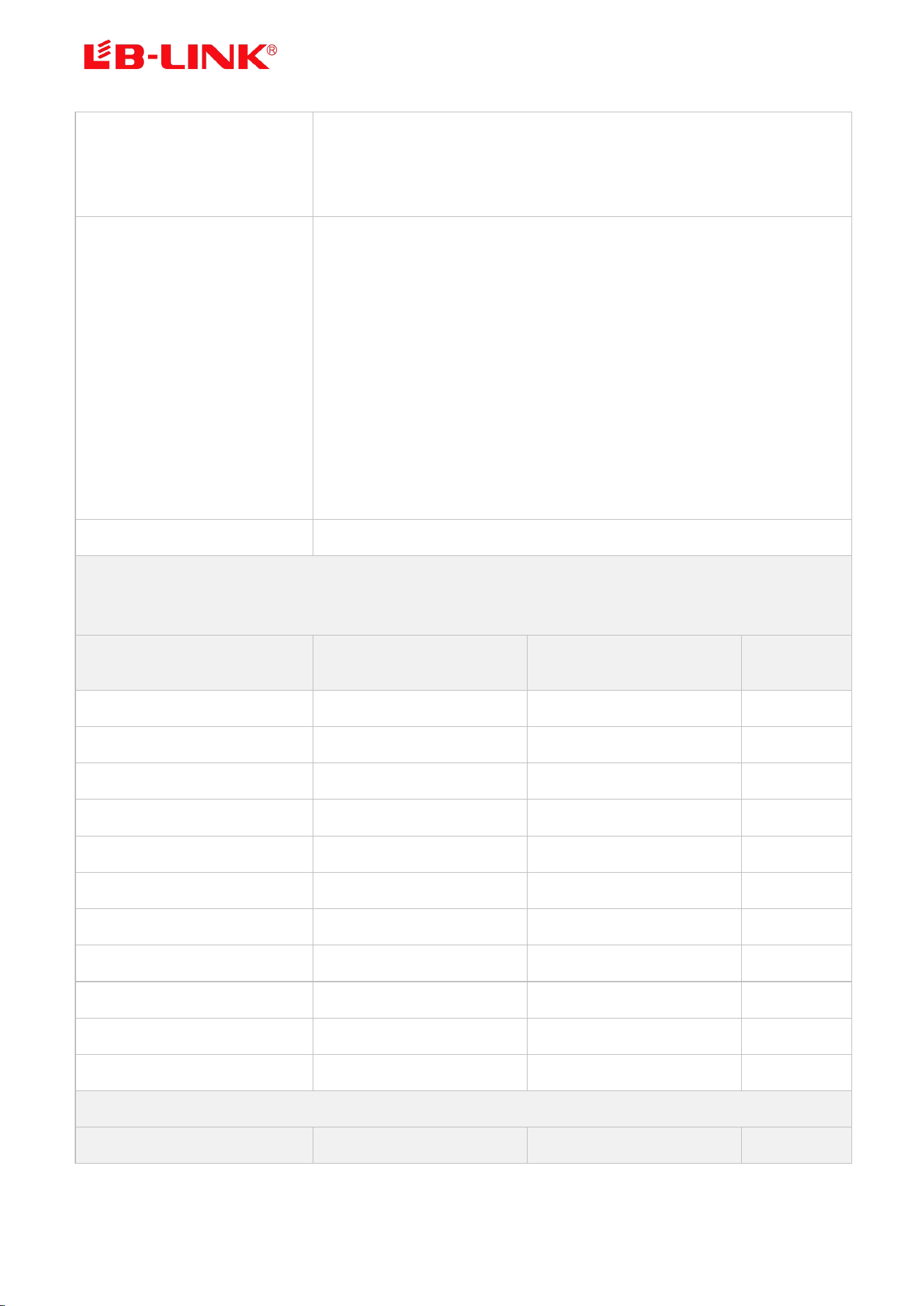
4. WALN & Bluetooth RF Specifications
4.1 2.4G WLAN RF Specification
Conditions : VDD33=3.3V ; Ta:25℃
Features
Description
WLAN Standard
IEEE 802.11b/g/n/ax
Frequency Range
2.4~2.4835GHz (2.4GHz ISM Band)
Channels
Ch1~Ch13 (For 20MHz Channels)
Modulation
802.11b (DSSS): CCK, DQPSK, DBPSK;
8 http://www.b-link.net.cn
802.11g (OFDM): BPSK, QPSK, QAM16, QAM64;
802.11n (OFDM): BPSK, QPSK, QAM16, QAM64;
802.11ax (OFDMA): BPSK, BPSK_DCM, QPSK, QPSK_DCM, QAM16,
QAM16_DCM, QAM64, QAM256, QAM1024;
Data Rate
802.11b: 1, 2, 5.5, 11Mbps;
802.11g: 6, 9, 12, 18, 24, 36, 48, 54Mbps;
802.11n (HT20): MCS0~MCS7(1T1R_SISO) 6.5~72.2Mbps;
802.11n (HT20): MCS8~MCS15(2T2R_MIMO) 13~144.4Mbps;
802.11n (HT40): MCS0~MCS7(1T1R) 13.5~150Mbps;
802.11n (HT40): MCS8~MCS15(2T2R) 27~300Mbps;
802.11ax (HE_MU,26~242RU): MCS0~MCS11(1T1R) 0.4~143.4Mbps;
802.11ax (HE_MU,26~242RU): MCS0~MCS11(2T2R) 0.8~286.8Mbps;
802.11ax (HE_SU, non-OFDMA 20MHz): MCS0~MCS11(1T1R) 3.6~143.4Mbps;
802.11ax (HE_SU, non-OFDMA 20MHz): MCS0~MCS11(2T2R) 7.3~286.8Mbps;
802.11ax (HE_SU, non-OFDMA 40MHz): MCS0~MCS11(1T1R) 7.3~286.8Mbps;
802.11ax (HE_SU,non-OFDMA 40MHz): MCS0~MCS11(2T2R) 14.6~573.5Mbps;
Frequency Tolerance
≦±20ppm
2.4G Transmitter Specifications(ANT0 & ANT1. TX power tolerance calibrated, customers can define the
target TX power by modifying configuration file of the driver software. Customers must define the TX
power same or lower than recommended Target TX Power as below)
TX Rate
Recommended Target TX
Power(dBm)
TX Power Tolerance(dBm)
EVM(dB)
802.11b@1~11Mbps
18
±2
≦ -15
802.11g@6Mbps
18
±2
≦ -15
802.11g@54Mbps
17
±2
≦ -25
802.11n@HT20_MCS0
18
±2
≦ -10
802.11n@HT20_MCS7
17
±2
≦ -28
802.11n@HT40_MCS0
17
±2
≦ -10
802.11n@HT40_MCS7
16
±2
≦ -28
802.11ax@HE_SU 20M_MCS0
16
±2
≦ -15
802.11ax@HE_SU 20M_MCS11
15
±2
≦ -35
802.11ax@HE_SU 40M_MCS0
16
±2
≦ -15
802.11ax@HE_SU 40M_MCS11
15
±2
≦ -35
2.4G Receiver Specifications(ANT0&ANT1)
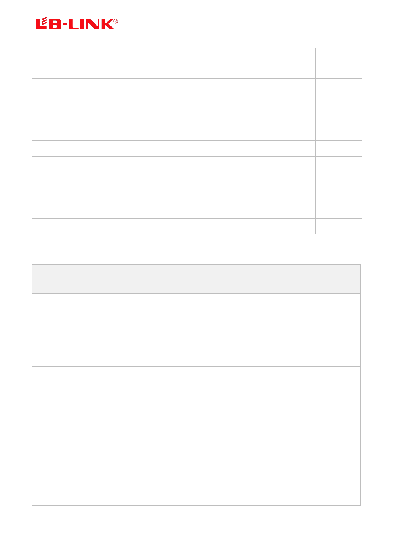
RX Rate
Min Input Level(Typ.dBm)
Max Input Level(Typ.dBm)
PER
9 http://www.b-link.net.cn
802.11b@1Mbps
-94
-5
< 8%
802.11b@11Mbps
-90
-5
< 8%
802.11g@6Mbps
-93
-5
< 10%
802.11g@54Mbps
-75
-5
< 10%
802.11n@HT20_MCS0
-92
-5
< 10%
802.11n@HT20_MCS7
-73
-5
< 10%
802.11n@HT40_MCS0
-91
-5
< 10%
802.11n@HT40_MCS7
-70
-5
< 10%
802.11ax@HE_SU 20M_MCS0
-90
-5
< 10%
802.11ax@HE_SU 20M_MCS11
-62
-5
< 10%
802.11ax@HE_SU 40M_MCS0
-89
-5
< 10%
802.11ax@HE_SU 40M_MCS11
-60
-5
< 10%
4.2 5G WLAN RF Specification
Conditions: VDD33 =3.3V; Ta:25℃
Features
Description
WLAN Standard
IEEE 802.11a/n/ac/ax
Frequency Range
5.15~5.25GHz; 5.25~5.35GHz; 5.47~5.725GHz;
5.725~5.850GHz (5GHz ISM Band)
Channels
Ch36, Ch40, Ch44, Ch48; Ch52~Ch64;
Ch100~Ch140; Ch149~Ch165 (For 20MHz Channels)
Modulation
802.11a (OFDM): BPSK, QPSK, QAM16, QAM64;
802.11n (OFDM): BPSK, QPSK, QAM16, QAM64;
802.11ac (OFDM): BPSK, QPSK, QAM16, QAM64, QAM256;
802.11ax (OFDMA): BPSK, BPSK_DCM, QPSK, QPSK_DCM, QAM16,
QAM16_DCM, QAM64, QAM256, QAM1024;
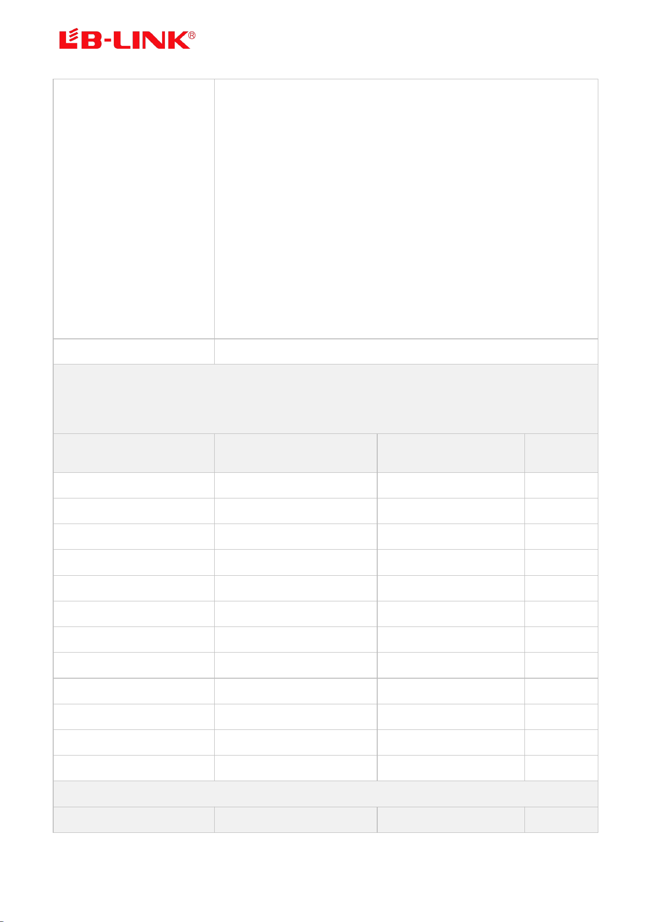
Data Rate
802.11a: 6, 9, 12, 18, 24, 36, 48, 54Mbps;
802.11n (HT20): MCS0~MCS7(1T1R_SISO) 6.5~72.2Mbps;
802.11n (HT20): MCS8~MCS15(2T2R_MIMO) 13~144.4Mbps;
802.11n (HT40): MCS0~MCS7(1T1R) 13.5~150Mbps;
802.11n (HT40): MCS8~MCS15(2T2R) 27~300Mbps;
802.11ac (VHT20): MCS0~MCS8(1T1R) 6.5~86.7Mbps;
10 http://www.b-link.net.cn
802.11ac (VHT20): MCS0~MCS8(2T2R) 13~173.3Mbps;
802.11ac (VHT40): MCS0~MCS9(1T1R)13.5~200Mbps;
802.11ac (VHT40): MCS0~MCS9(2T2R)27~400Mbps;
802.11ac (VHT80): MCS0~MCS9(1T1R)29.3~433.3Mbps;
802.11ac (VHT80): MCS0~MCS9(2T2R)58.5~866.7Mbps;
802.11ax (HE_MU,26~484RU): MCS0~MCS11(1T1R) 0.4~286.8Mbps;
802.11ax (HE_MU,26~484RU): MCS0~MCS11(2T2R) 0.8~573.5Mbps;
802.11ax (HE_SU, non-OFDMA 20MHz): MCS0~MCS11(1T1R) 3.6~143.4Mbps;
802.11ax (HE_SU, non-OFDMA 20MHz): MCS0~MCS11(2T2R) 7.3~286.8Mbps;
802.11ax (HE_SU, non-OFDMA 40MHz): MCS0~MCS11(1T1R) 7.3~286.8Mbps;
802.11ax (HE_SU,non-OFDMA 40MHz): MCS0~MCS11(2T2R) 14.6~573.5Mbps;
802.11ax (HE_SU,non-OFDMA 80MHz): MCS0~MCS11(1T1R) 15.3~600.4Mbps;
802.11ax (HE_SU, non-OFDMA 80MHz): MCS0~MCS11(2T2R) 30.6~1201Mbps;
Frequency Tolerance
≦ ±20ppm
5G Transmitter Specifications(ANT0 & ANT1. TX power tolerance calibrated, customers can define the target
TX power by modifying configuration file of the driver software. Customers must define the TX power same
or lower than recommended Target TX Power as below)
TX Rate
Recommended Target TX
Power(dBm)
TX Power Tolerance(dBm)
EVM(dB)
802.11a@6Mbps
18
±2
≦ -10
802.11a@54Mbps
17
±2
≦ -25
802.11n@HT20_MCS0
17
±2
≦ -13
802.11n@HT20_MCS7
16
±2
≦ -28
802.11n@HT40_MCS0
17
±2
≦ -13
802.11n@HT40_MCS7
16
±2
≦ -28
802.11ac@VHT20_MCS0
17
±2
≦ -13
802.11ac@VHT20_MCS8
16
±2
≦ -30
802.11ac@VHT80_MCS0
17
±2
≦ -13
802.11ac@VHT80_MCS9
16
±2
≦ -32
802.11ax@HE_SU80_MCS0
16
±2
≦ -13
802.11ax@HE_SU80_MCS11
15
±2
≦ -35
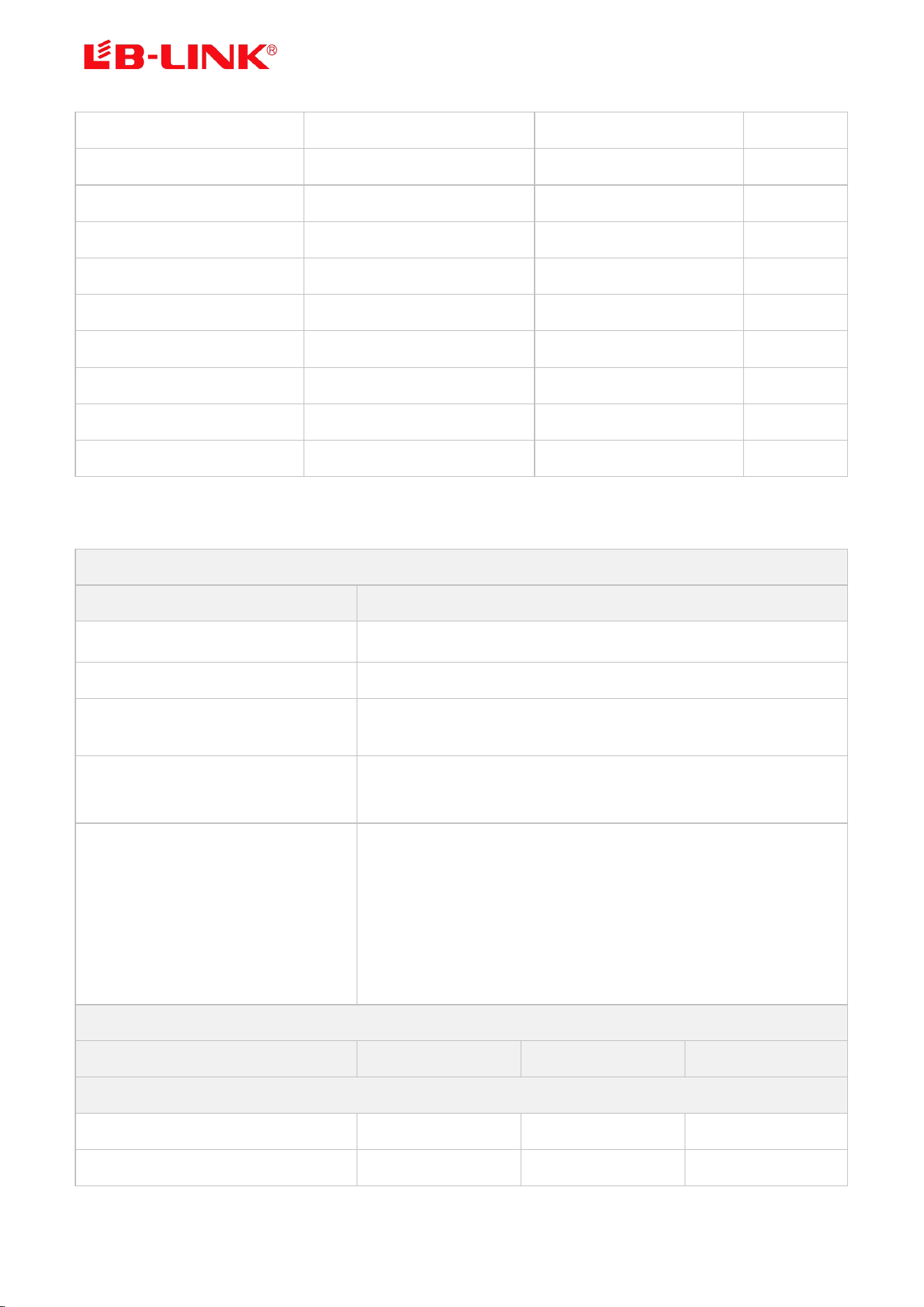
5G Receiver Specifications(ANT0&ANT1)
RX Rate
Min Input Level(Typ.dBm)
Max Input Level(Typ.dBm)
PER
11 http://www.b-link.net.cn
802.11a@6Mbps
-91
-5
< 10%
802.11a@54Mbps
-74
-5
< 10%
802.11n@HT20_MCS0
-92
-5
< 10%
802.11n@HT20_MCS7
-72
-5
< 10%
802.11n@HT40_MCS0
-89
-5
< 10%
802.11n@HT40_MCS7
-69
-5
< 10%
802.11ac@VHT80_MCS0
-85
-5
< 10%
802.11ac@VHT80_MCS9
-60
-5
< 10%
802.11ax@HE_SU80_MCS0
-86
-5
< 10%
802.11ax@HE_SU80_MCS11
-58
-5
< 10%
4.3 Bluetooth RF Specification
Conditions: VDD33=3.3V; Ta:25℃
Features
Description
Bluetooth Specification
Bluetooth Core Specification v5.2/4.2/2.1
Frequency Range
2.4~2.4835GHz (2.4GHz ISM Band)
Channels
Bluetooth Classic: Ch0~Ch78 (For 1MHz Channels);
Bluetooth Low Energy: Ch0~Ch39 (For 2MHz Channels);
Power Classes
Bluetooth Classic: Class1;
Bluetooth Low Energy: Class1.5;
Data Rate & Modulation
BR_1Mbps: GFSK;
EDR_2Mbps: π/4-DQPSK;
EDR_3Mbps: 8DPSK;
LE_125Kbps: GFSK (Coded_S=8);
LE_500Kbps: GFSK (Coded_S=2);
LE_1Mbps: GFSK (Uncoded);
LE_2Mbps: GFSK (Uncoded);
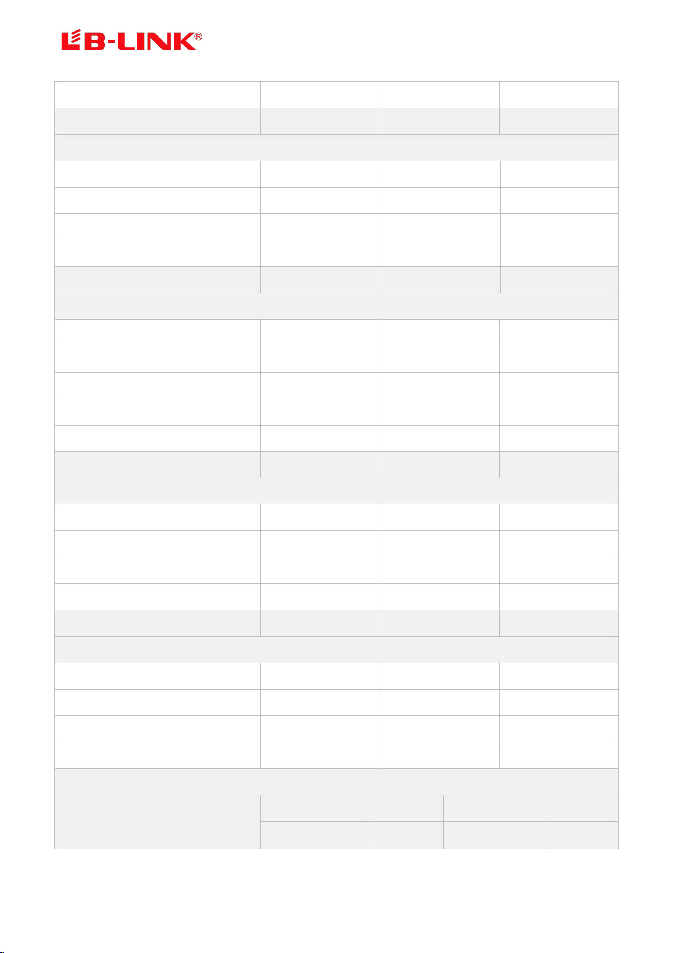
Bluetooth Transmitter Specifications (BT ANT)
Items
Min(dBm)
Typ(dBm)
Max(dBm)
TX Power
BR_1M
0
5
10
EDR_2/3M
0
5
10
12 http://www.b-link.net.cn
LE_125K/500K/1M/2M
0
5
10
Items
Min
Typ
Max
BR_1M (DH1) Modulation Characteristics
Δf1avg
140KHz
162.48KHz
175KHz
Δf2avg
115KHz
152.11KHz
175KHz
Δf2max
115KHz
160.83KHz
/
Δf2avg/Δf1avg
0.8
0.93
/
Items
Min
Typ
Max
EDR_3M(3DH5) EDR Carrier Frequency Stability and Modulation Accuracy
ωi
-75KHz
-16.57KHz
+75KHz
ωi+ωo
-75KHz
-16.62KHz
+75KHz
ωo
-10KHz
-0.07KHz
+10KHz
8DPSK RMS DEVM
/
0.037
0.13
8DPSK DEVM
/
0.082
0.25
Items
Min
Typ
Max
LE_1M Modulation Characteristics
Δf1avg
225KHz
252.15KHz
275KHz
Δf2avg
185KHz
230.44KHz
275KHz
Δf2max
185KHz
223.41KHz
/
Δf2avg/Δf1avg
0.8
0.91
/
Items
Min
Typ
Max
LE_2M Modulation Characteristics
Δf1avg
450KHz
499.54KHz
550KHz
Δf2avg
370KHz
495.81KHz
550KHz
Δf2max
370KHz
478.32KHz
/
Δf2avg/Δf1avg
0.8
0.99
/
Bluetooth Receiver Specifications(BT ANT)
Items
Sensitivity
Maximum Input Level
Input Level(dBm)
BER
Input Level(dBm)
BER
13 http://www.b-link.net.cn
BR_1M (DH1)
-70
≦ 0.1%
-5
≦ 0.1%
EDR_2M(DH1)
-70
≦ 0.01%
-10
≦ 0.1%
EDR_3M (3DH5)
-65
≦ 0.01%
-5
≦ 0.1%
Input Level (dBm)
PER
Input Level (dBm)
PER
LE_125/500K
-70
≦ 5%
-5
≦ 5%
LE_1M
-70
≦ 5%
-5
≦ 5%
LE_2M
-65
≦ 5%
-5
≦ 5%
5. Mechanical Specifications
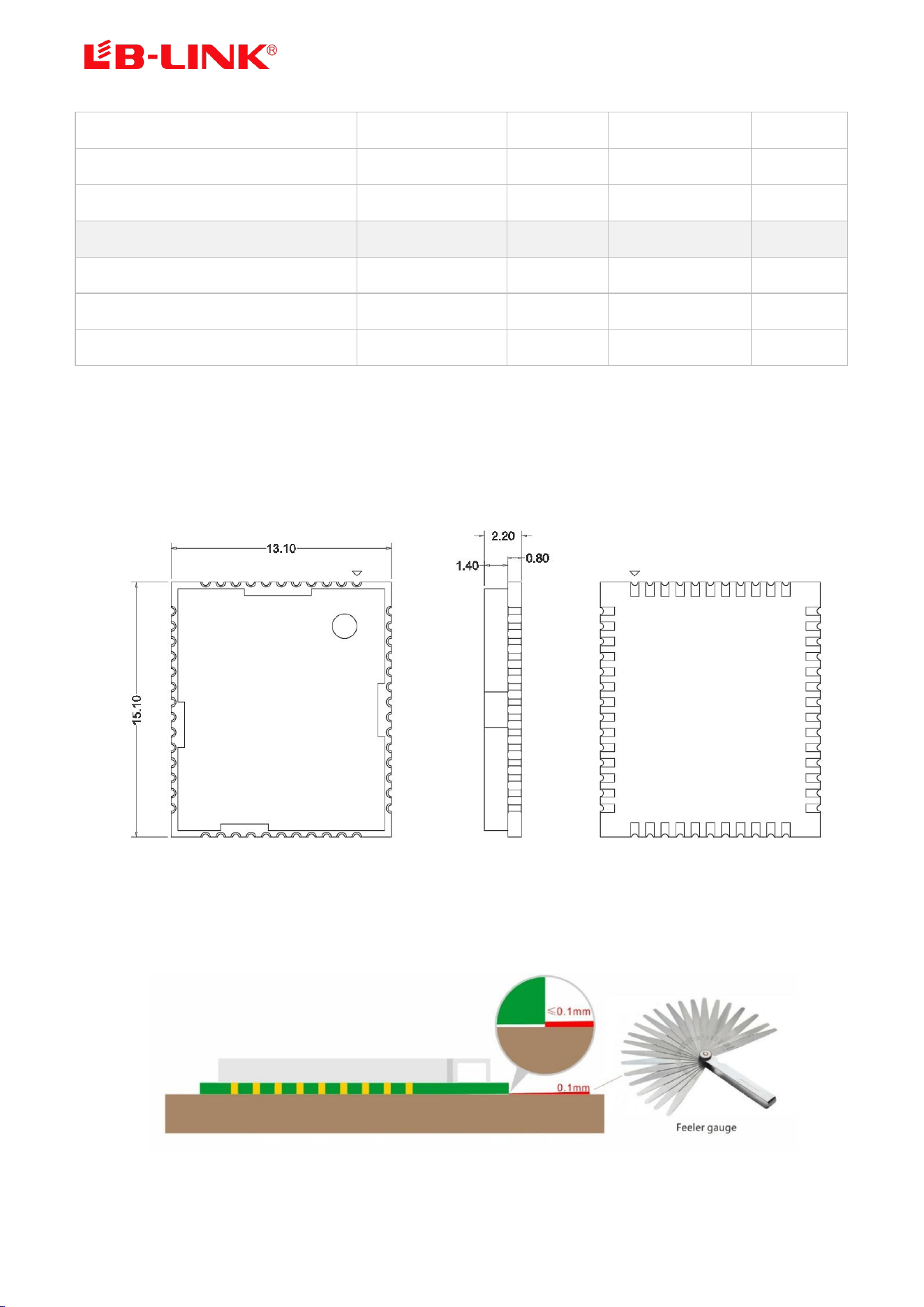
5.1 Module Outline Drawing
(Top View) (Side View) (Bottom View)
Module dimension: 15.1*13.1*2.2mm(L*W*H; Tolerance: ±0.3mm_L/W, ±0.2mm_H)
Module Bow and Twist:≤0.1mm
14 http://www.b-link.net.cn
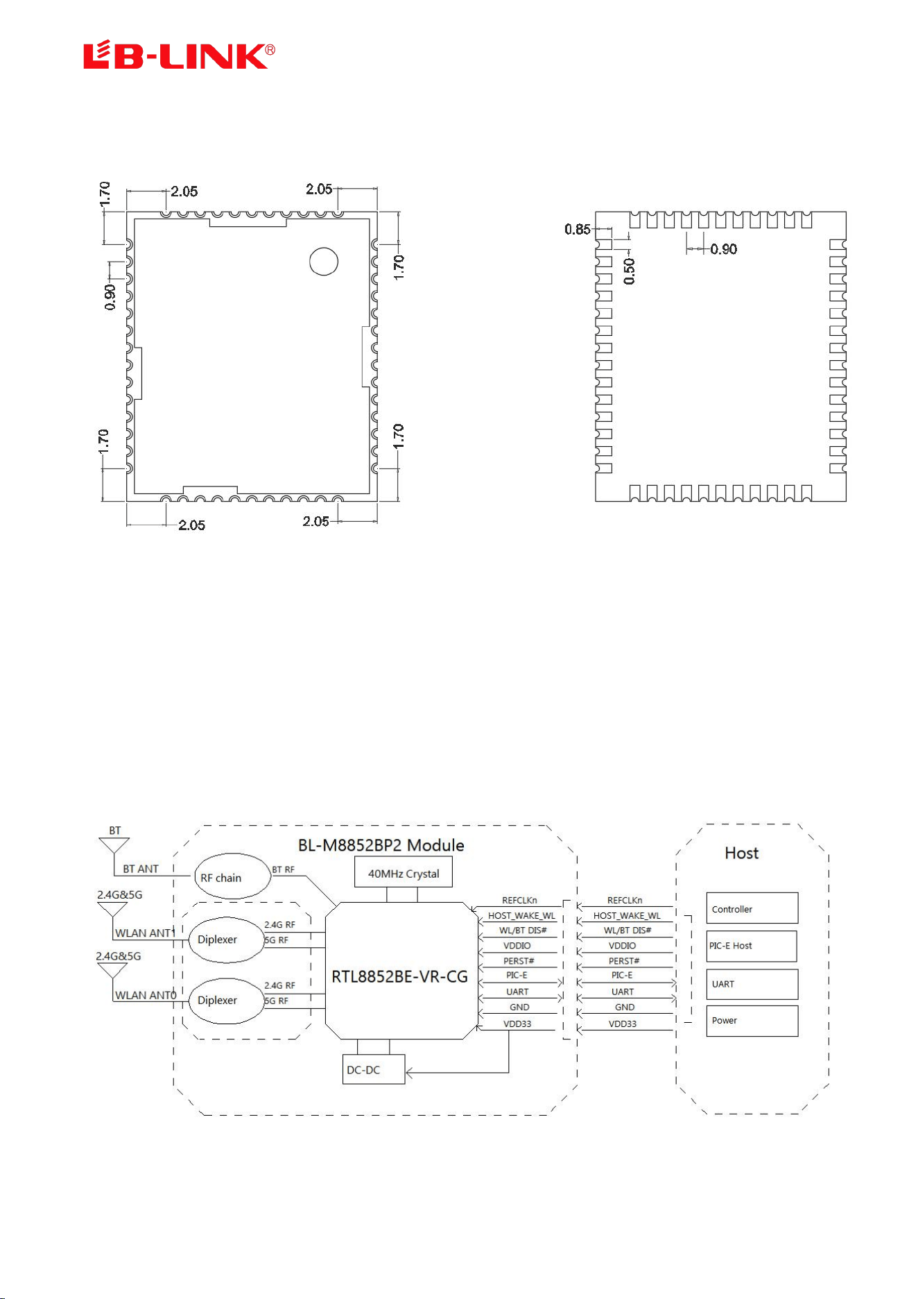
5.2 Mechanical Dimensions
(Top View) (Bottom View)
6. Application Information
6.1 Typical Application Circuit
15 http://www.b-link.net.cn
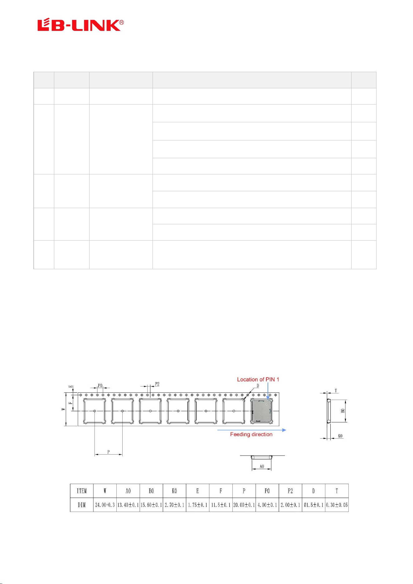
6.2 Recommend PCB Layout Footprint
(Design Unit: mm)
6.3 Reflow Soldering Standard Conditions
Please use the reflow within 2 times.
Set up the highest temperature within 250℃.
16 http://www.b-link.net.cn
7. Key Components Of Module
No.
Parts
Specification
Manufacturer
Note
1
Chipset
RTL8852BE-VR-CG
Realtek Semiconductor Corp.
2
PCB
BL-M8852BP2
ShenZhen Tie Fa Technology Limited
Huizhou Dayawan Kexiang Technology Circuit Board Co., Ltd
Quzhou Sunlord Electronics Co.,Ltd
SHEN ZHEN QILI ELECTRON CO., LTD
3
Crystal
40MHz-2016
JinHua East Crystal Electronic CO.,LTD
Chengde Oscillator Electronic Technology Co., Ltd.
4
Diplexer
1608
JIA XING GLEAD ELECTRONICS CO.,LTD
Dongguan Hekang Electronics Co.,LTD
5
Power
inductor
2.2uH
Shenzhen Jialan Microelectronics Co., Ltd
Note: To ensure supply chain stability, certified alternative components with potential cosmetic variations have
been utilized. The physical appearance of the module shall be governed by the final delivered unit.
8. Package and Storage Information
8.1 Package Dimensions
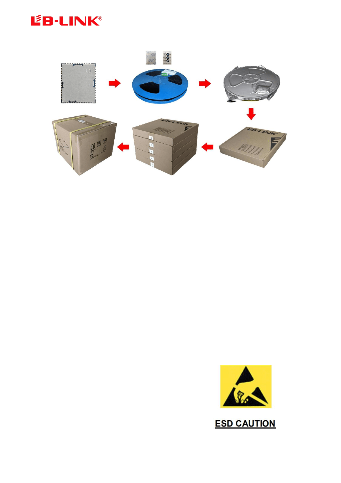
17 http://www.b-link.net.cn
Package specification:
1. 1,000 modules per roll and 5,000 modules per box.
2. Outer box size: 37.5*36*29cm.
3. The diameter of the blue environment-friendly rubber plate is 13 inches, with a total thickness of 28mm (with a
width of 24mm carrying belt).
4. Put 1 package of dry agent (20g) and humidity card in each anti-static vacuum bag.
5. Each carton is packed with 5 boxes.
8.2 Storage Conditions
Absolute Maximum Ratings:
Storage temperature: -40℃ to +85℃,
Storage humidity: 10% to 95(Non-Condensing)
Recommended Storage Conditions:
Storage temperature: 5℃ to +40℃,
Storage humidity: 20% to 90% RH
Please use this Module within 12month after vacuum-packaged.
The Module shall be stored without opening the packing.
After the packing opened, the Module shall be used within 72hours.
When the color of the humidity indicator in the packing changed,
The Module shall be baked before soldering.
Baking condition: 60℃, 24hours, 1time.
ESD Sensitivity:
ESD Protection: 2KV (HBM, Maximum rating)
The Module is a static-sensitive electronic device.
Do not operate or store near strong electrostatic fields.
Take proper ESD precautions!

18 http://www.b-link.net.cn
The Module is designed to comply with the FCC statement. FCC ID is 2AL6K-BLM8852BP2. The host system
using Module, should have label indicated it contain modular’s FCC ID: 2AL6K-BLM8852BP2. This radio module
must not installed to collocate and operating simultaneously with other radios in host system additional testing and
equipment authorization may be required to operating simultaneously with other radio.
The Module and its antenna must not be co-located or operating in conjunction with any other transmitter or
antenna within a host device.
The modular must be installed in the host that assign by Company name: Shenzhen Bilian Electronic Co.,Ltd.,
Model no.: BL-M8852BP2 if other host types used would need further evaluation and possible C2PC if they are not
significantly similar to the one tested The WIFI Module is designed for a compact PCB design. It should be
installed and operated with host or other minimum distance of 20 centimeters between the radiator and your body."
To comply with FCC regulations limiting both maximum RF output power and human exposure to RF radiation,
the maximum antenna gain including cable loss in a mobile-only exposure condition must not exceed 2 dBi in BT,
3 dBi in2.4G WIFI, 3 dBi in the 5G WIFI. The module uses FPC antenna and Copper tube antenna, these antennas
are sold with the module.
Notice to OEM integrator
The end user manual shall include all required regulatory information/warning as show in this manual. The OEM
integrator is responsible for testing their end-product for any additional compliance requirements required with this
module installed. If the final product contains circuits of other FCC PART 15 Subparts, the final host product still
requires Part 15 Subpart B compliance testing with the modular transmitter installed The intended use is generally
not for the general public. It is generally for industry/commercial use. The connector is within the transmitter
enclosure and can only be accessed by disassembly of the transmitter that is not normally required, the user has no
access to the connector. Installation must be controlled. Installation requires special training.
This device complies with Part 15 of the FCC Rules.
This equipment should be installed and operated with a minimum distance of 20 cm between the radiator and your
body.
2.2
This module has been assessed against the following FCC rule parts: CFR 47 FCC Part 15 C (15.247. DTS) and
CFR 47 FCC Part 15 E (NlI). lt is applicable to the modular transmitter
2.3
This radio transmitter Module has been approved by Federal Communications Commission to operate with the
antenna types listed below, with the maximum permissible gain indicated. Antenna types not included in this list
that have a gain greater than the maximum gain indicated for any type listed are strictly prohibited for use with this
device.
The concrete contents to check are the following three points.
1) Maximum antenna gains are shown in item 2.7 below.
2) Should be installed so that the end user cannot modify the antenna
3) Feed line should be designed in 50ohm
Fine-tuning of return loss etc. can be performed using a matching network.
The antenna shall not be accessible for modification or change by the end user.

19 http://www.b-link.net.cn
2.4
The module complies with FCC Part 15.247 / Part 15.407 and apply for Single module approval.
2.5
Trace antenna designs: applicable.
Any deviation(s) from the defined parameters of the antenna trace, as described by the instructions, require that the
host product manufacturer must notify the module grantee that they wish to change the antenna trace design. in this
case, a Class ll permissive change application is required to be filed by the grantee, or the host manufacturer can
take responsibility through the change in FCC lD (new application) procedure followed by a Class ll permissive
change application.
The device must be professionally installed.
The intended use is generally not for the general public.
It is generally for industry/commercial use.
The connector is within the transmitter enclosure and can only be accessed by disassembly of the transmitter that is
not normally required.
The user has no access to the connector.
Installation must be controlled.
Installation requires special training.
2.6
This equipment complies with FCC radiation exposure limits set forth for an uncontrolled environment. This
equipment should be installed and operated with a minimum distance of 20cm between the radiator & your body.
This transmitter must not be co-located or operating in conjunction with any other antenna or transmitter.
2.7
The following antennas have been certified for use with this module.
Only antennas of the same type with equal or lower gain may also be used with this module.
Other types of antennas and/or higher gain antennas may require the additional authorization for operation. The
installer should use unique antenna connector and Antenna types not included in this list that have a gain greater
than the maximum gain indicated for any type listed are strictly prohibited for use with this device. The
manufacturer of module will inform installer to meet with the FCC part 15.203 in the warning part.
Antenna Specification list below:
BT:
Antenna type: FPC Antenna
The max antenna gain (in dBi):
BR+EDR: 2 dBi
BLE: 2 dBi
2.4G WIFI:
Antenna type: Copper tube antenna
The max antenna gain (in dBi):
3 dBi for antenna 1

20 http://www.b-link.net.cn
3 dBi for antenna 2
5G WIFI:
Antenna type: Copper tube antenna
The max antenna gain (in dBi):
3 dBi for antenna 1
3 dBi for antenna 2
2.8
Please notice that if the FCC identification number is not visible when the module is installed inside another device,
then the outside of the device into which the module is installed must also display a label referring to the enclosed
module. This exterior label can use wording such as "Contains FCC ID: 2AL6K-BLM8852BP2 "; any similar
wording that expresses the same meaning may be used.
2.9
Testing of the host product with all the transmitters installed - referred to as the composite investigation test- is
recommended, to verify that the host product meets all the applicable FCC rules. The radio spectrum is to be
investigated with all the transmitters in the final host product functioning to determine that no emissions exceed the
highest limit permitted for any one individual transmitter as required by Section 2.947(f). The host manufacturer is
responsible to ensure that when their product operates as intended it does not have any emissions present that are
out of compliance that were not present when the transmitters were tested individually.
If the modular transmitter has been fully tested by the module grantee on the required number of channels,
modulation types, and modes, it should not be necessary for the host installer to re-test all the available transmitter
modes or settings. lt is recommended that the host product manufacturer, installing the modular transmitter,
perform some investigative measurements to confirm that the resulting composite system does not exceed the
spurious emissions limits or band edge limits (e.g., where a different antenna may be causing additional emissions).
The testing should check for emissions that may occur due to the intermixing of emissions with the other
transmitters, digital circuitry, or due to physical properties of the host product (enclosure). This investigation is
especially important when integrating multiple modular transmitters where the certification is based on testing each
of them in a stand-alone configuration.
2.10
Any company of the host device which install this modular should perform the test of radiated & conducted
emission and spurious emission etc. according to FCC Part 15C: 15.247 and15.209 & 15.207, part 15E: 15.407,
part 15B: class B requirement, only if the test result comply with FCC part 15C: 15.247 and 15.209 & 15.207 part
15 E 15.407, 15B class B requirement. Then the host can be sold legally.
The host product manufacturer is responsible for compliance to any other FCC rules that apply to the host not
covered by the modular transmitter grant of certification, lf the grantee markets their product as being Part 15
Subpart B compliant (when it also contains unintentional-radiator digital circuity), then the grantee shall provide a
notice stating that the final host product still
requires Part 15 Subpart B compliance testing with the modular transmitter installed.

21 http://www.b-link.net.cn
FCC Statement
1. This device complies with Part 15 of the FCC Rules. Operation is subject to the following two conditions:
(1)This device may not cause harmful interference.
(2)This device must accept any interference received, including interference that may cause undesired operation.
2. Changes or modifications not expressly approved by the party responsible for compliance could void the user’s
authority to operate the equipment.
Note: This equipment has been tested and found to comply with the limits for a class B digital device, pursuant to
Part 15 of the FCC Rules. These limits are designed to provide reasonable protection against harmful interference
in a residential installation.
This equipment generates uses and can radiate radio frequency energy and, if not installed and used in accordance
with the instructions, may cause harmful interference to radio communications. However, there is no guarantee that
interference will not occur in a particular installation. If this equipment does cause harmful interference to radio or
television reception, which can be determined by turning the equipment off and on, the user is encouraged to try to
correct the interference by one or more of the following measures:
• Reorient or relocate the receiving antenna.
• Increase the separation between the equipment and receiver.
• Connect the equipment into an outlet on a circuit different from that to which the receiver is connected.
• Consult the dealer or an experienced radio/TV technician for help.
The device has been evaluated to meet general RF exposure requirement. This equipment should be installed and
operated with a minimum distance of 20 cm between the radiator and your body.
ISED Statement
This device contains licence-exempt transmitter(s)/receiver(s) that comply with Innovation, Science and
Economic Development Canada’s licence-exempt RSS(s). Operation is subject to the following two
conditions:
1. This device may not cause interference.
2. This device must accept any interference, including interference that may cause undesired operation of
the device.
The device has been evaluated to meet general RF exposure requirement. This equipment should be
installed and operated with a minimum distance of 20 cm between the radiator and your body.
L’émetteur/récepteur exempt de licence contenu dans le présent appareil est conforme aux CNR
d’Innovation, Sciences et Développement économique Canada applicables aux appareils radio exempts
de licence. L’exploitation est autorisée aux deux conditions suivantes :
1) L’appareil ne doit pas produire de brouillage;
2) L’appareil doit accepter tout brouillage radioélectrique subi, même si le brouillage est
susceptible d’en compromettre le fonctionnement.
Le dispositif a été évalué pour répondre aux exigences générales d'exposition aux ondes radiofréquence

22 http://www.b-link.net.cn
s.Cet équipement doit être installé et utilisé avec une distance minimale de 20 cm entre le radiateur et
votre corps.
Operations in the 5.15-5.25GHz band are restricted to indoor usage only.
Les opérations dans la bande 5.15-5.25GHz sont limitées à une utilisation à l’intérieur seulement.
The Module is designed to comply with the ISED statement. IC is 20944-BLM8852BP2. The host system using
Module, should have label indicated it contain modular's IC: 20944-BLM8852BP2. This radio module must not
installed to collocate and operating simultaneously with other radios in host system additional testing and
equipment authorization may be required to operating simultaneously with other radio.
The Module and its antenna must not be co-located or operating in conjunction with any other transmitter or
antenna within a host device.
This radio transmitter [IC: 20944-BLM8852BP2] has been approved by Innovation, Science and Economic
Development Canada to operate with the antenna types listed below, with the maximum permissible gain indicated.
Antenna types not included in this list that have a gain greater than the maximum gain indicated for any type listed
are strictly prohibited for use with this device.
The modular must be installed in the host that assign by Company name: Shenzhen Bilian Electronic Co.,Ltd.,
Model no.: BL-M8852BP2. If other host types used would need further evaluation and possible C2PC if they are
not significantly similar to the one tested The WIFI Module is designed for a compact PCB design. It should be
installed and operated with host or other minimum distance of 20 centimeters between the radiator and your body.
To comply with ISED regulations limiting both maximum RF output power and human exposure to RF radiation,
the maximum antenna gain including cable loss in a mobile-only exposure condition must not exceed 2 dBi in BT,
3 dBi in2.4G WIFI, 3 dBi in the 5G WIFI. The module uses FPC antenna and Copper tube antenna, these antennas
are sold with the module.