
www.wireless-tag.com
2
WIRELESS-TAG
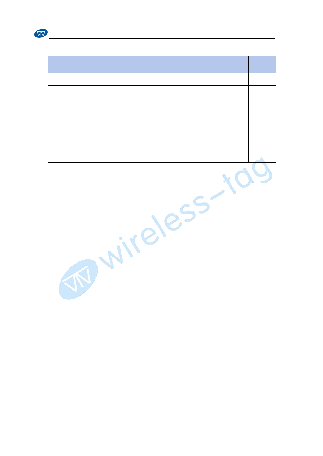
WT0132C5-S5 Series Datasheet
Disclaimer and Copyright Notice
Information in this document, including the URL addresses for reference,
is subject to change without notice.
This document is provided "as is" without warranty of any kind, including
any warranty of merchantability, fitness for a particular purpose, or
non-infringement, and any warranty that any proposal, specification, or sample
is referred to elsewhere. this document disclaims all liability, including liability
for infringement of any patent, arising out of the use of the information in this
document. This document does not grant any license, express or implied, by
estoppel or otherwise, to use any intellectual property.
The Wi-Fi Alliance member logo is owned by the Wi-Fi Alliance.
All trade names, trademarks and registered trademarks mentioned herein
are the property of their respective owners and are hereby acknowledged.
Notice
The content of this manual is subject to change due to product version
upgrade or other reasons. WIRELESS-TAG Technology Co.,limited reserves
the right to modify the contents of this manual without any notice or prompting.
Ltd. makes every effort to provide accurate information in this manual, but
WIRELESS-TAG Technology Co.,limited does not ensure that the contents of
the manual are completely free of errors, and all statements, information and
recommendations in this manual do not constitute any express or implied
warranty.
www.wireless-tag.com
3
WIRELESS-TAG
WT0132C5-S5 Series Datasheet
Revision History
Version
Date
Developed/ Changed Content
Modifier By
Auditor
V0.1
2025-6-4
First Creation(Preview)
Pail
Louie
V0.2
2025-7-16
Modify 4.3.Recommended Working
Conditions
Pail
Louie
V1.0
2025-8-4
Official Release
Pail
Louie
V1.1
2025-9-2
Update 1.3. Product Pictures
Modify 3.2. Pin Descriptions
Modify 5. WT0132C5-S5 Schematic
Pail
Louie

www.wireless-tag.com
4
WIRELESS-TAG
WT0132C5-S5 Series Datasheet
Contents
1. Overview
......................................................... 5
1.1. Products Introduction
......................................... 5
1.2. Product Features
............................................ 6
1.3. Product Pictures
............................................. 6
1.4. Application Scenarios
.........................................7
2. Product Specification
...............................................7
2.1. Block Diagram
..............................错误!未定义书签。
2.2. Hardware Parameters
........................................ 7
3. Pin Definitions
.....................................................7
3.1. Pin Layout
.................................................. 7
3.2. Pin Description
.............................................. 8
3.3. Startup Item Configuration
.................................... 9
3.3.1. Strapping Pins
......................................... 9
3.3.2. Chip Boot Mode Control
................................ 12
3.3.3. ROM Messages Printing Control
........................ 12
3.3.4. JTAG Signal Source Control
............................ 13
3.3.5. Crystal Frequency Selection
............................ 14
4. Electrical Characteristics
...........................................15
4.1. Absolute Maximum Limit Value
............................... 15
4.2. Power Consumption Characteristics
........................... 15
4.3. Recommended Working Conditions
........................... 15
5. WT0132C5-S5 Schematic
......................... 错误!未定义书签。
6. WT0132C5-S5 Dimensions
........................ 错误!未定义书签。
7. Storage Condition
................................................ 16
8. Reflow Soldering Curve
........................................... 17
9. Contact Us
.......................................................17
10. Manufacturer's name and address
................................. 17
11. Warning
........................................................ 18
www.wireless-tag.com
5
WIRELESS-TAG
WT0132C5-S5 Series Datasheet
1. Overview
1.1.Products Introduction
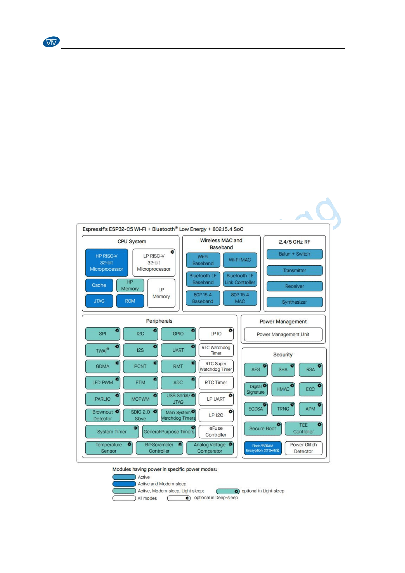
WT0132C5-S5 series module is an integrated dual-band Wi-Fi & BLE
module designed based on Espressif ESP32-C5 series chipset launched by
Wireless-Tag Technology Co.,Limited.The WT0132C5-S5 supports 2.4 & 5G
Wi-Fi6 (802.11ax), Bluetooth®5 (LE), Zigbee, and Thread (802.15.4), and is
powerful with a rich set of peripheral interfaces supporting PCB antennae or
I-PEX (Generation 3) RF coaxial connectors, and is designed for Internet of
Things (IoT), industrial automation, healthcare, andconsumer electronics
applications.
Figure 1: Main Chip Architecture Diagram
www.wireless-tag.com
6
WIRELESS-TAG
WT0132C5-S5 Series Datasheet
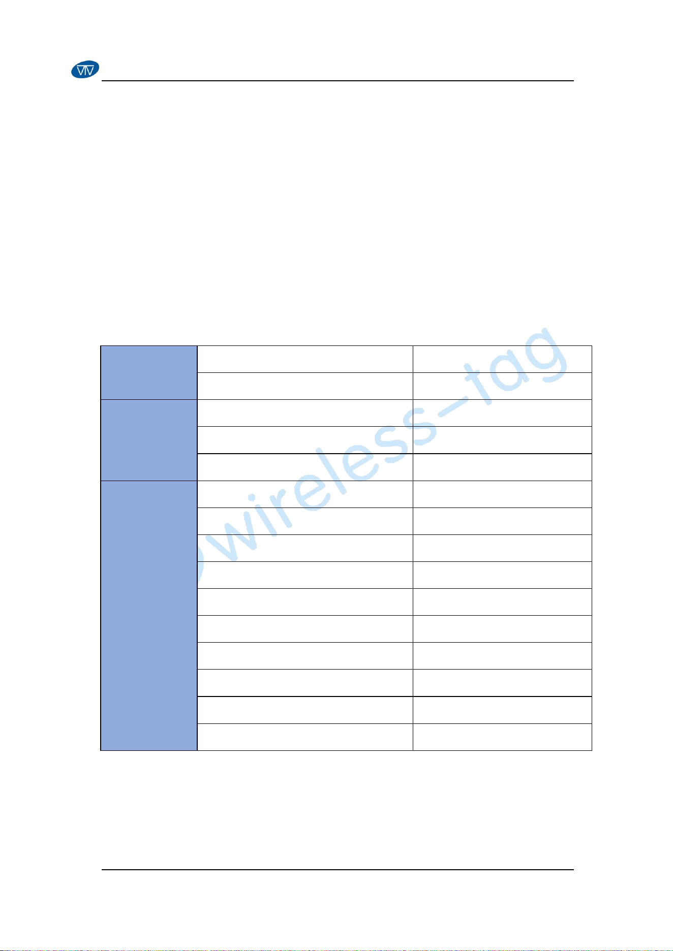
The WT0132C5-S5 series is available in two sizes, see the table below for
more information.
WT0132C5-S5 Series Model Number Comparison
Part Number
Flash
Antenna
Module Size (mm)
WT0132C5-S5-N4
4MB
PCB
24.00*16.00
WT0132C5-S5U-N4
4MB
IPEX
24.00*16.00
1.2.Product Features
RISC-V 32-bit single-core processor at 240 MHz
RISC-V MCU supporting 2.4GHz & 5GHz Wi-Fi6, BLE5, IEEE 802.15.4
supports PCB antenna or I-PEX RF coaxial connector.
Mature software support, based on Espressif’s ESP-IDF IoT development
framework.
Complete security mechanism, including secure boot, flash encryption and
hardware encryption gas pedal.
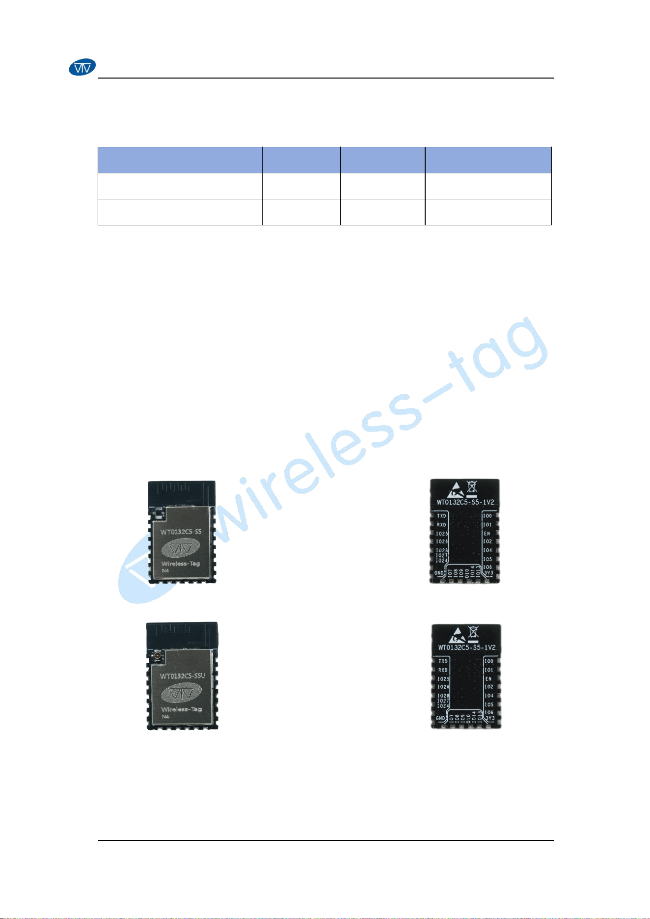
1.3.Product Pictures
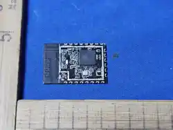
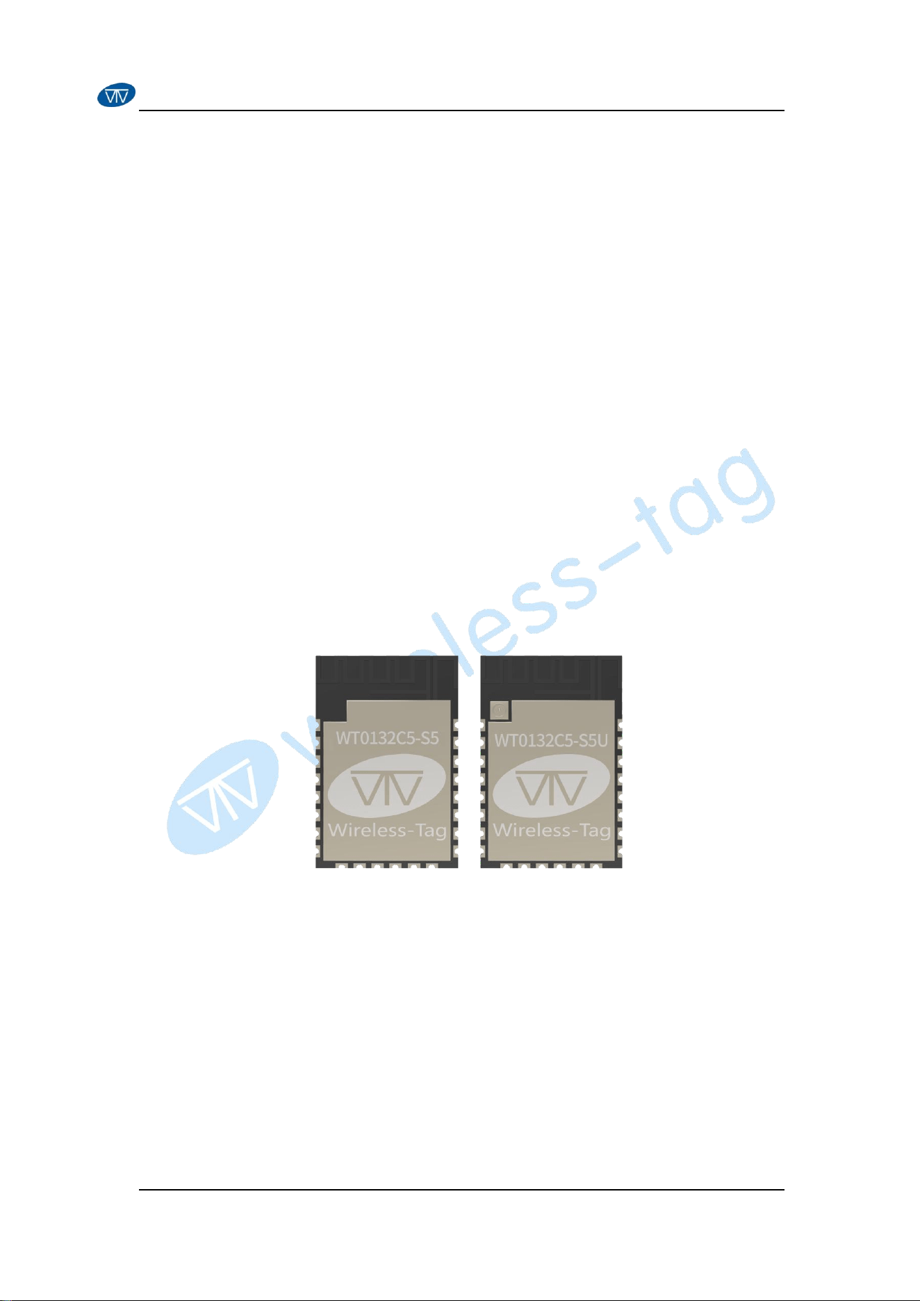
Figure 2:WT0132C5-S5-N4(front) Figure 3:WT0132C5-S5-N4 (back)
Figure 4:WT0132C5-S5U-N4(front) Figure 5:WT0132C5-S5U-N4(back)
www.wireless-tag.com
7
WIRELESS-TAG
WT0132C5-S5 Series Datasheet
1.4.Application Scenarios
Smart Home
Industrial Automation
Consumer Electronics
HMI Human Machine Interaction
Healthcare
Mobile Pay
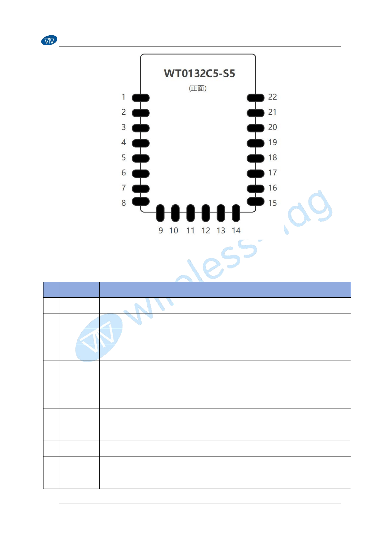
2. Product Specification
2.1.Hardware Parameters
CPU
Core
32-bit RISC-V dual-core
Main Frequency
240 MHz
Memory
ROM
320 KB
SRAM
384 KB
Flash
4MB
Peripheral
Interface
GPIO
17
SPI
1
UART
2
I2C
1
I2S
1
SDIO Slave
1
LED PWM
1
MCPWM
1
12-bit multi-channel ADC
1
Temperature sensor
1
3. Pin Definitions
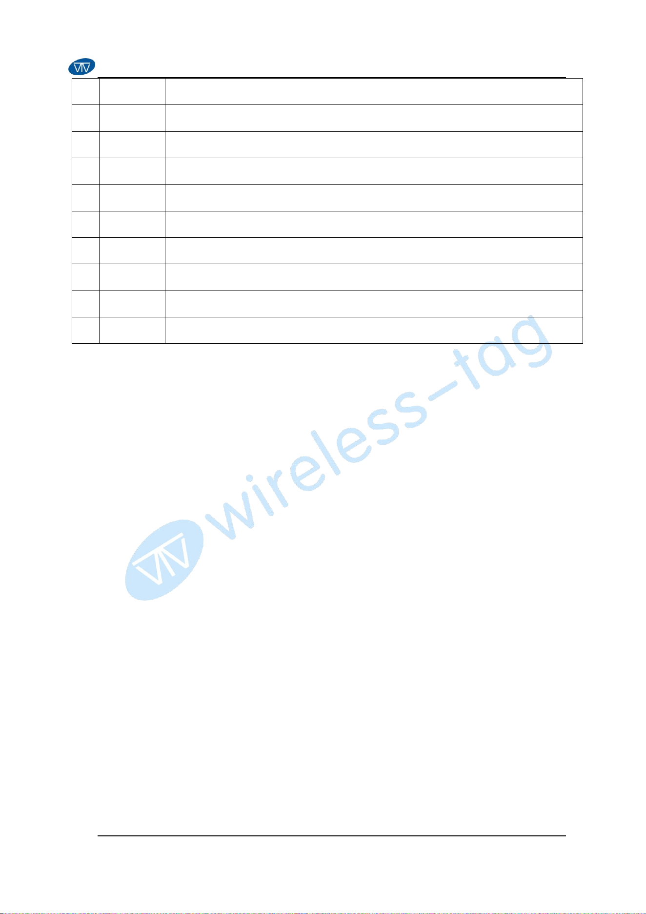
3.1.Pin Layout
www.wireless-tag.com
8
WIRELESS-TAG
WT0132C5-S5 Series Datasheet
Figure 7:WT0132C5-S5 Pin Layout
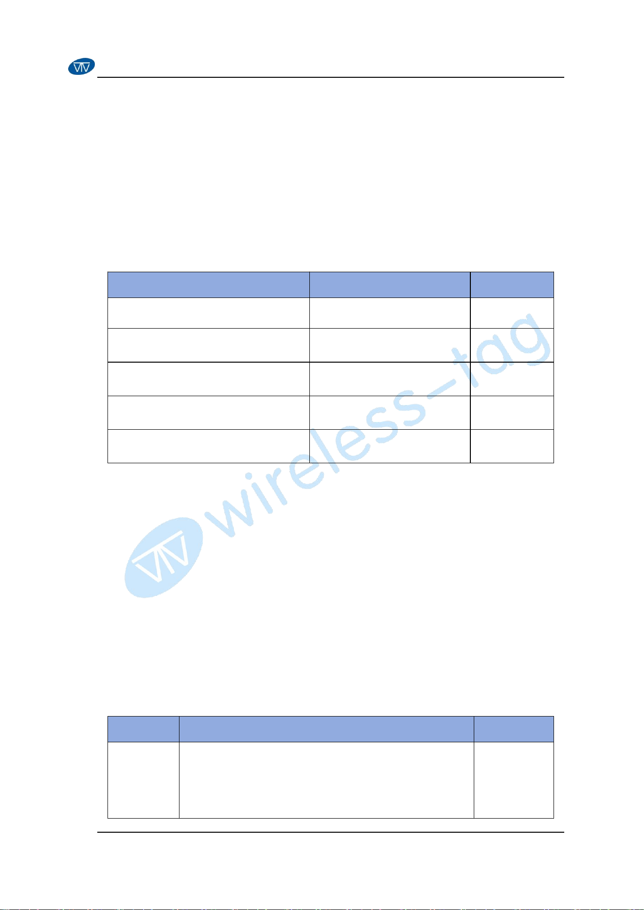
3.2.Pin Description
Pin Definitions
No.
Name
Function
1
GPIO0
GPIO0
,
LP_GPIO0, XTAL_32K_P, LP_UART_DTRN
2
GPIO1
GPIO1
,
LP_GPIO1, XTAL_32K_N, LP_UART_DSRN, ADC1_CHO
3
CHIP_EN
Enable ESP32-C5 chip (internal 10K pull-up)
4
GPIO2
GPIO2
,
LP_GPIO2
,
MTMS
,
LP_UART_RTSN
,
ADC1_CH1
,
FSPIQ
5
GPIO4
GPIO4
,
LP_GPIO4
,
LP_UART_RXD
,
MTCK
,
ADC1_CH3
,
FSPIHD
6
GPIO5
GPIO5,LP_GPIO5,LP_UART_TXD,MTDO,ADC1_CH4,FSPIWP
7
GPIO6
GPIO6,LP_GPIO6,LP_I2C_SDA,ADC1_CH5,FSPICLK
8
VDD33
POWER(3.3V input)
9
GPIO13
GPIO13,USB_D-,SDIO_DATA3
10
GPIO14
GPIO14,USB_D+,SDIO_DATA2
11
GPIO10
GPIO10,SDIO_CMD,FSPICS0
12
GPIO9
GPIO9
,
PAD_COMP1
,
SDIO_CLK
www.wireless-tag.com
9
WIRELESS-TAG
WT0132C5-S5 Series Datasheet
13
GPIO8
GPIO8
,
PAD_COMP0
,
SDIO_DATA0
14
GPIO7
GPIO8,SDIO_DATA1,FSPID
15
GND
GROUND
16
GPIO24
GPIO24
17
GPIO27
GPIO27
18
GPIO28
GPIO28
19
GPIO26
GPIO26
20
GPIO25
GPIO25
21
U0RXD
GPIO12,U0RXD
22
U0TXD
GPIO11,U0TXD
3.3.Startup Item Configuration
3.3.1. Strapping Pins
The chip allows for configuring the following boot parameters through
strapping pins and eFuse bits at power-up or a hardware reset, without
microcontroller interaction.
Chip Boot Mode
– Strapping pin: GPIO26, GPIO27 and GPIO28
ROM Message Printing
– Strapping pin: GPIO27
– eFuse parameter:
EFUSE_UART_PRINT_CONTROL and EFUSE_DIS_USB_SERIAL_JTAG_ROM_PRINT
JTAG signal source
– Strapping pin: GPIO7
– eFuse parameter:
EFUSE_DIS_PAD_JTAG, EFUSE_DIS_USB_JTAG, and EFUSE_JTAG_SEL_ENABLE
Crystal frequency selection
– Strapping pin: MTMS(effective only in Joint Download Boot mode)
– eFuse parameter:EFUSE_XTAL_48M_SEL and EFUSE_XTAL_48M_SEL_MODE
www.wireless-tag.com
10
WIRELESS-TAG
WT0132C5-S5 Series Datasheet
The default values of all the above eFuse parameters are 0, which means
that they are not burnt. Given that eFuse is one-time programmable, once
programmed to 1, it can never be reverted to 0.
The default values of the strapping pins, namely the logic levels, are
determined by pins’internal weak pull-up/pull-down resistors at reset if the pins
are not connected to any circuit, or connected to an external high-impedance
circuit.
Default Configuration of Strapping Pin
Strapping Pin
Default Configuration
Value
GPIO26
Floating
-
GPIO27
Weak pull-up
1
GPIO28
Weak pull-up
1
GPIO7
Floating
-
MTMS
Floating
-
To change the bit values, the strapping pins should be connected to external
pull-down/pull-up resistors.
All strapping pins have latches. At system reset, the latches sample the bit
values of their respective strapping pins and store them until the chip is powered
down or shut down. The states of latches cannot be changed in any other way. It
makes the strapping pin values available during the entire chip operation, and the
pins are freed up to be used as regular IO pins after reset.
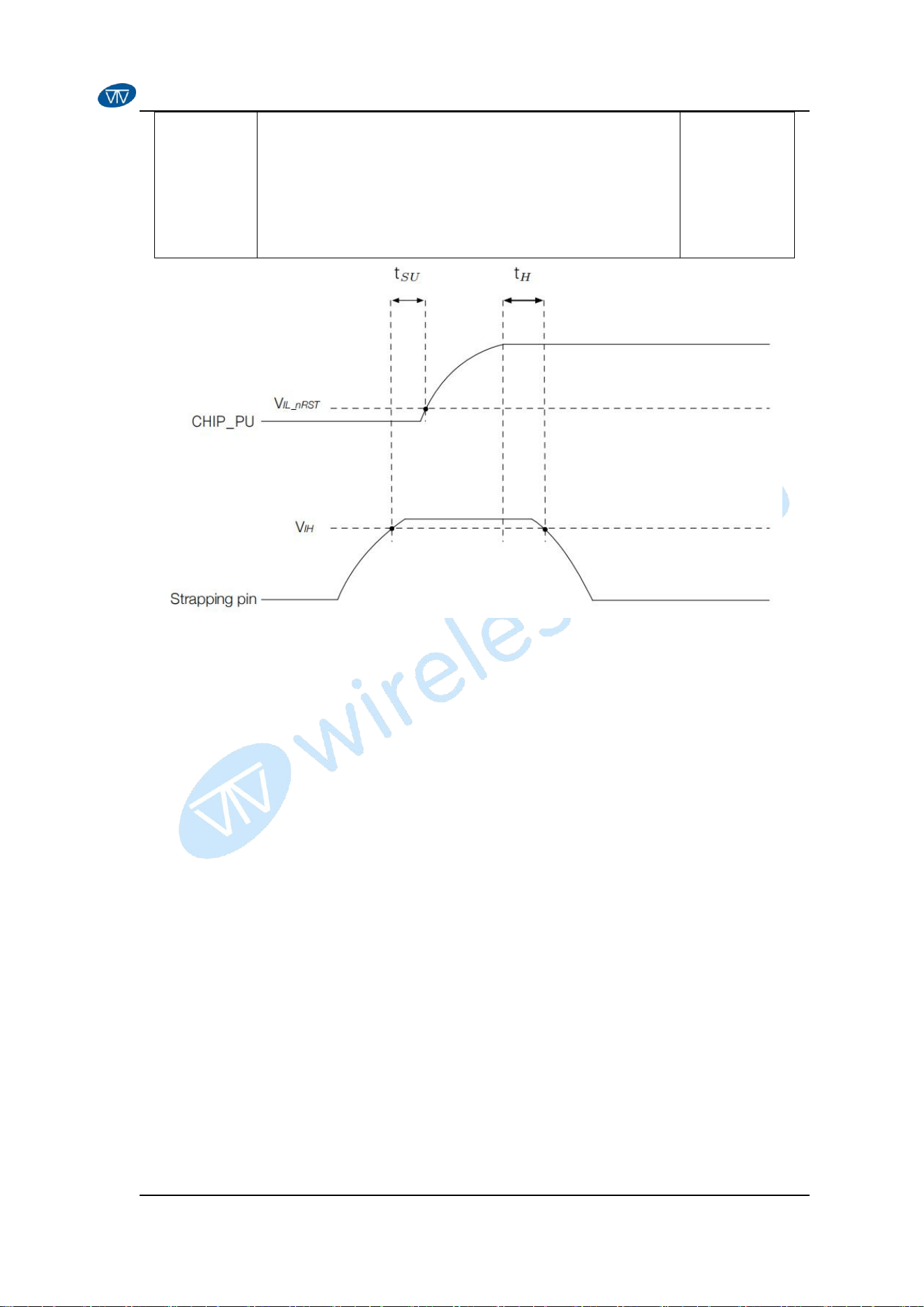
The timing of signals connected to the strapping pins should adhere to the
setup time and hold time specifications in Table and Figure 8.
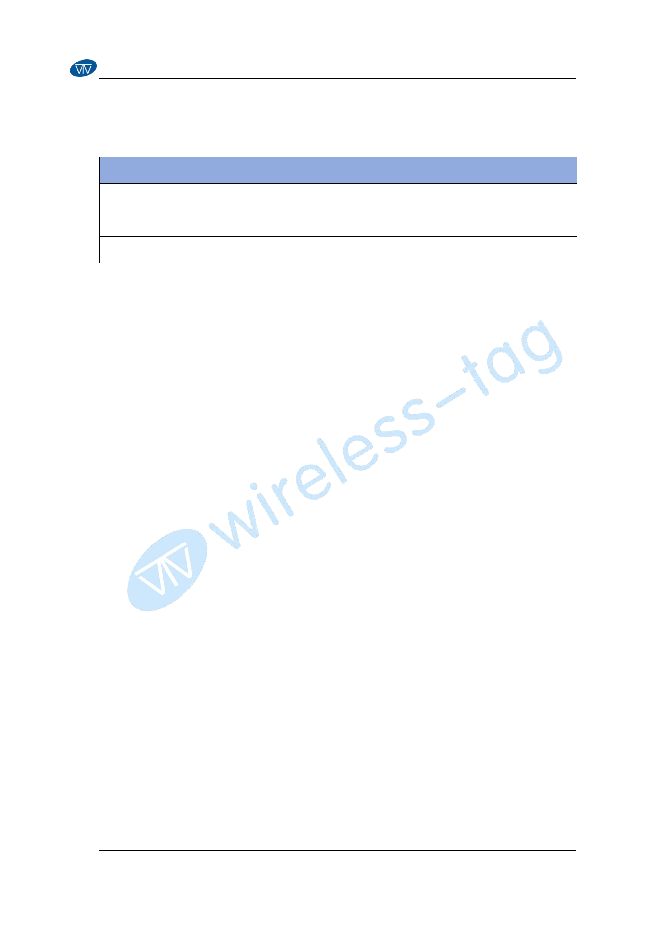
Description of Timing Parameters for the Strapping Pins
Parameter
Description
Min(ms)
t
SU
Setup time is the time reserved for the power rails
to stabilize before the CHIP_PU pin is pulled high
to activate the chip.
0
www.wireless-tag.com
12
WIRELESS-TAG
WT0132C5-S5 Series Datasheet
3.3.2. Chip Boot Mode Control
GPIO27,GPIO26 and GPIO28 control the boot mode after the reset is
released.
Boot Mode
GPIO26
GPIO27
GPIO28
SPI Boot*
Any value
Any value
1*
Joint Download Boot 0
Any value
1
0
Joint Download Boot 1
0
0
0
*marks the default value and configuration.
Joint Download Boot mode 0 supports the following download methods:
USB-Serial-JTAG Download Boot
UART Download Boot
Joint Download Boot mode 1 supports the following download methods:
UART Download Boot
SDIO Download Boot
In SPI Boot mode, the ROM bootloader loads and executes the program from
SPI flash to boot thesystem.
In Joint Download Boot 0 mode, users can download binary files into flash
using UART0 or USB interfaces. It is also possible to download binary files into
SRAM and execute it from SRAM.
In Joint Download Boot 1 mode, users can download binary files into flash
using UART0 or SDIO interfaces. It is also possible to download binary files into
SRAM and execute it from SRAM.
3.3.3. ROM Messages Printing Control
During the boot process, the messages by the ROM code can be printed to:
(Default) UART0 and USB Serial/JTAG controller
USB Serial/JTAG controller
UART0
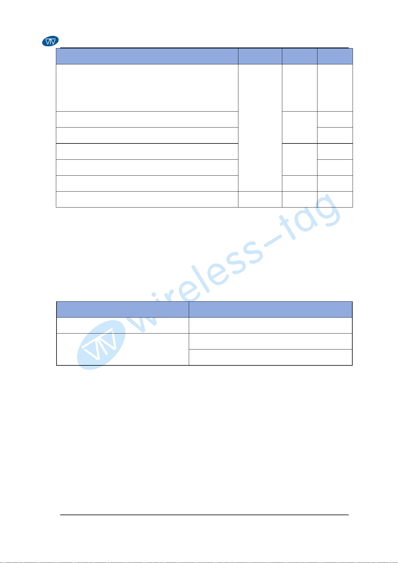
EFUSE_UART_PRINT_CONTROL and GPIO27 control ROM messages
printing to UART0 as shown in Table.
www.wireless-tag.com
13
WIRELESS-TAG
WT0132C5-S5 Series Datasheet
UART0 Code Printing
Register
2
eFuse
3
GPIO27
ROM messages are always printed to UART0 during
boot
*
0
*
0
(
0b00)
*
X
4
Print is enabled during boot
1(0b01)
0
Print is disabled during boot
1
Print is disabled during boot
2
(
0b10)
0
Print is enabled during boot
1
Print is disabled during boot
3
(
0b11)
x
Print is disabled during boot
1
x
x
*marks the default value and configuration.
2
Register: LP_AON_STORE4_REG[0]
3
eFuse: EFUSE_UART_PRINT_CONTROL
4
x: x indicates that the value has no effect on the result and can be ignored
EFUSE_DIS_USB_SERIAL_JTAG_ROM_PRINT controls the printing to
USB Serial/JTAG controller as shown in Table.
USB Serial/JTAG ROM Code Printing
EFUSE_DIS_USB_SERIAL_JTAG_ROM_PRINT
Enabled*
0*
Disabled
1
Ignored
*marks the default value and configuration.
3.3.4. JTAG Signal Source Control
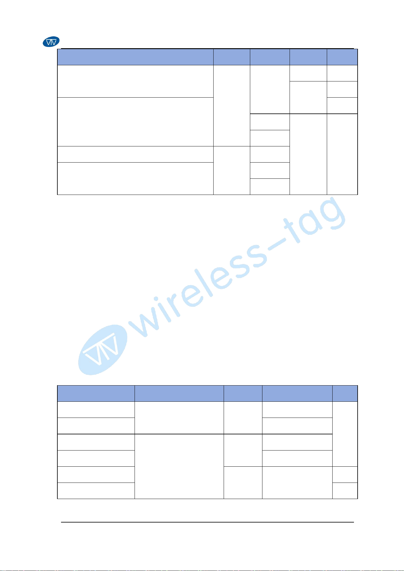
The strapping pin GPIO7 can be used to control the source of JTAG signals
during the early boot process. This pin does not have any internal pull resistors
and the strapping value must be controlled by the external circuit that cannot be in
a high impedance state.
GPIO7 is used in combination with
EFUSE_DIS_PAD_JTAG,EFUSE_DIS_USB_JTAG, and EFUSE_JTAG_SEL_ENABLE.
www.wireless-tag.com
14
WIRELESS-TAG
WT0132C5-S5 Series Datasheet
JTAG Signal Source
eFuse 1
2
eFuse 2
3
eFuse 3
4
GPIO7
USB Serial/JTAG Controller
*6
0*
0*
0*
x
5
1
1
JTAG pins MTDI,MTCK,MTMS,and MTDO
0
x
x
x
1
USB Serial/JTAG Controller
6
1
0
JTAG is disabled
x
1
*marks the default value and configuration.
2
eFuse 1:EFUSE_DIS_PAD_JTAG
3
eFuse 2:EFUSE_DIS_USB_JTAG
4
eFuse 3:EFUSE_JTAG_SEL_ENABLE
5
x: x indicates that the value has no effect on the result and can be ignored
6
In Joint Download Boot 1 mode, the USB Serial/JTAG controller is forcibly
disabled, and the JTAG signal only comes from JTAG pins. If PAD_JTAG is also
disabled, then JTAG is disabled.
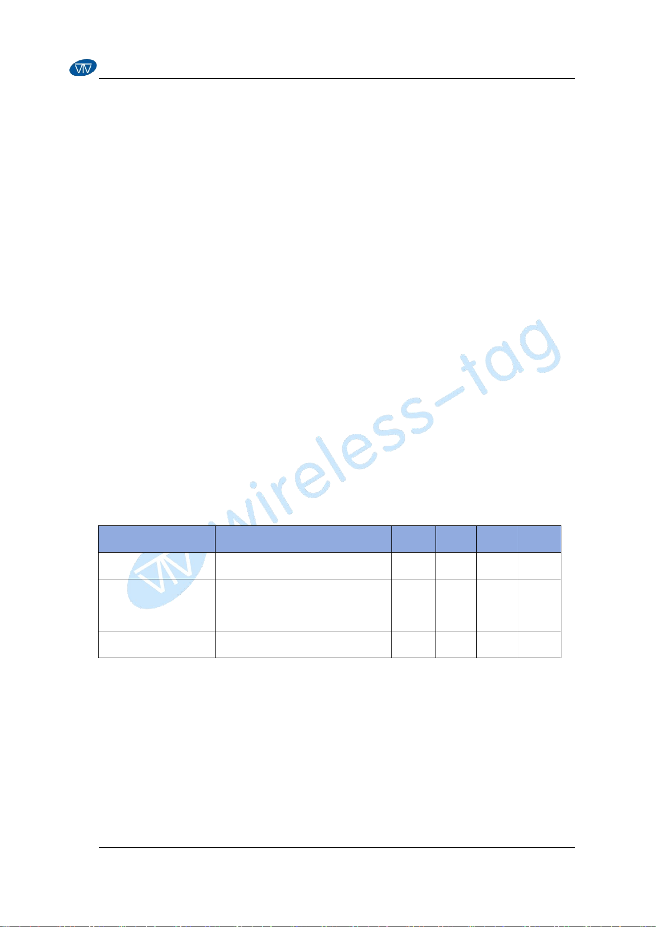
3.3.5. Crystal Frequency Selection
ESP32-C5 supports crystal frequencies of 40 MHz and 48 MHz. Boot modes
together with MTMS, EFUSE_XTAL_48M_SEL, and
EFUSE_XTAL_48M_SEL_MODE collectively control the crystal frequency.
Crystal Frequency
Boot Mode
eFuse 1
2
eFuse 2
3
MTMS
40 MHz
*
SPI Boot
*
x
4
Even number of 1
*
x
48 MHz
Odd number of 1
40 MHz
Joint Download Boot
0/1
1
Even number of 1
48 MHz
Odd number of 1
40 MHz
0*
x*
0
5
48 MHz
1
5
*marks the default value and configuration.
www.wireless-tag.com
15
WIRELESS-TAG
WT0132C5-S5 Series Datasheet
2
eFuse 1: EFUSE_XTAL_48M_SEL_MODE
3
eFuse 2: EFUSE_XTAL_48M_SEL
4
x: x indicates that the value has no effect on the result and can be ignored.
5
In Joint Download Boot 0/1 mode, users need to set the signal level on
MTMS strapping pin.
4. Electrical Characteristics
4.1.Absolute Maximum Limit Value
Exceeding the absolute maximum ratings may result in permanent damage
to the device. This is an emphasized rating only and does not address the
functional operation of the device under these or other conditions beyond those
indicated in these specifications. Prolonged exposure to absolute maximum rating
conditions may affect module reliability.
4.2.Power Consumption Characteristics
update soon
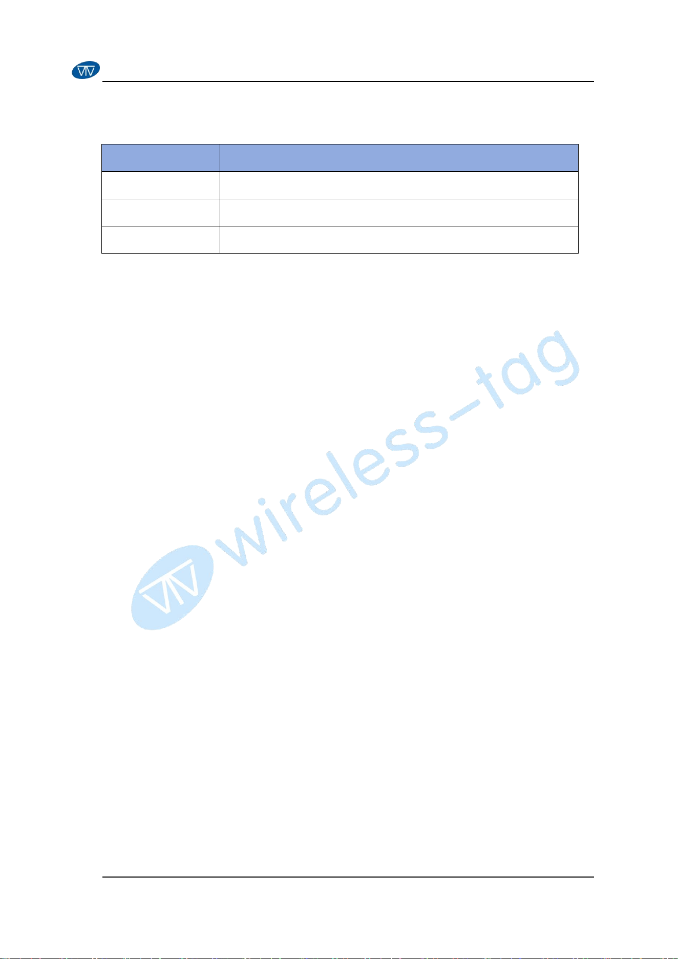
4.3.Recommended Working Conditions
Parameter
Description
Min
Typ
Max
Unit
VCC
Power pin voltage
3.0
3.3
3.6
V
I
VCC
Supply current from
external power supply
0.5
-
-
A
T
A
Operating Temperature
-40
-
85
℃
www.wireless-tag.com
17
WIRELESS-TAG
WT0132C5-S5 Series Datasheet
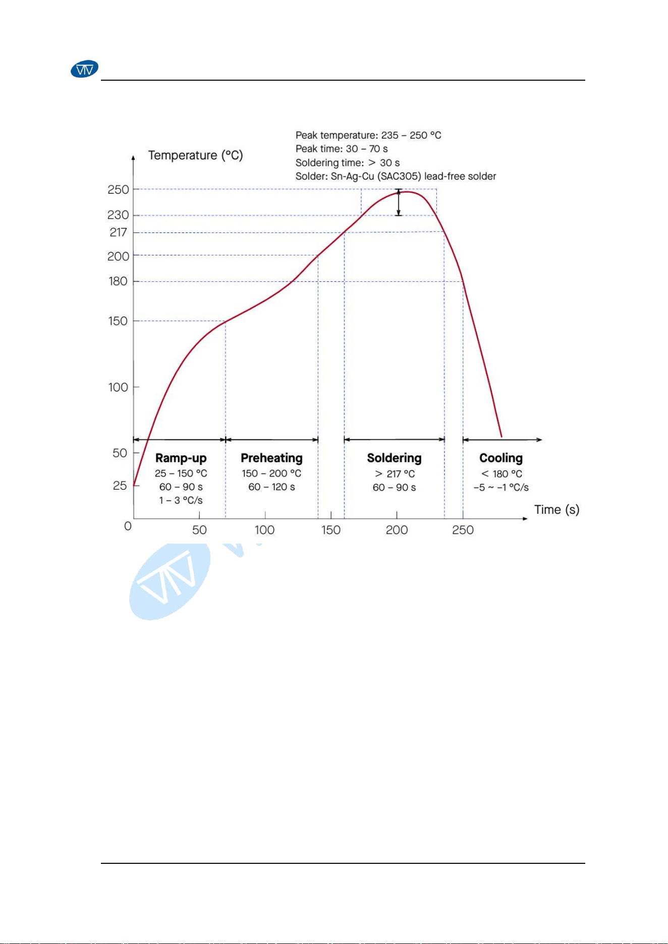
6. Reflow Soldering Curve
Figure 11: Reflow Soldering Temperature Curve
7. Contact Us
Official website: www.wireless-tag.com
Contact Email: gtm@wireless-tag.com
8. Manufacturer's name and address
WIRELESS-TAG Technology Co.,limited
801, Block A, Building 6, Shenzhen International Innovation Valley,
DashiRoad, Xili Community, Xili Street, Nanshan District, Shenzhen.

www.wireless-tag.com
18
WIRELESS-TAG
WT0132C5-S5 Series Datasheet
9. Warning
FCC
Changes or modifications not expressly approved by the party responsible for
compliance could void the user’s authority to operate the equipment.
This device complies with Part 15 of the FCC Rules. Operation is subject to
the following two conditions:
(1) this device may not cause harmful interference, and
(2) this device must accept any interference received, including interference
that may cause undesired operation.
Class B equipment warning message
Note: This equipment has been tested and found to comply with the limits for
a Class B digital device, pursuant to Part 15 of the FCC Rules. These limits are
designed to provide reasonable protection against harmful interference in a
residential installation. This equipment generates, uses, and can radiate radio
frequency energy, and if not installed and used in accordance with the instructions,
may cause harmful interference to radio communications. However, there is no
guarantee that interference will not occur in a particular installation. If this
equipment does cause harmful interference to radio or television reception, which
can be determined by turning the equipment off and on, the user is encouraged to
try to correct the interference by one or more of the following measures:
– Reorient or relocate the receiving antenna.
– Increase the separation between the equipment and receiver.
– Connect the equipment into an outlet on a circuit different from that to
which the receiver is connected.
– Consult the dealer or an experienced radio/TV technician for help.
FCC 20cm Statement
This equipment complies with FCC radiation exposure limits set forth for an

www.wireless-tag.com
19
WIRELESS-TAG
WT0132C5-S5 Series Datasheet
uncontrolled environment. This equipment should be installed and operated with a
minimum distance of 20cm between the radiator & your body. This transmitter
must not be co-located or operating in conjunction with any other antenna or
transmitter.
BLE Specification:
Operation Frequency: 2402~2480MHz
Number of Channel: 40
Modulation: GFSK
Zigbee Specification:
Operation Frequency: 2405~2480MHz
Number of Channel: 16
Modulation: GFSK
WiFi 2.4G Specification:
Operation Frequency: 2412-2472MHz(for EU),2412-2462MHz(for FCC)
Number of Channel: 13(for EU),11(for FCC)
Modulation: DSSS, OFDM
WiFi 5G Specification:
Operation Frequency: 5G(UINII-1): 5180-5240MHz &
5G(UINII-3):5745-5825MHz
Number of Channel: 5
Modulation: OFDM
www.wireless-tag.com
20
WIRELESS-TAG
WT0132C5-S5 Series Datasheet
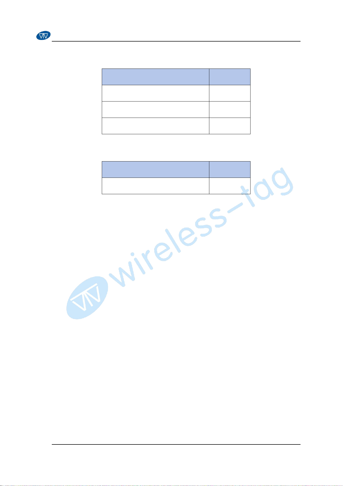
Wi-Fi Radio Frequency
2.4G Wi-Fi RF Transmitter and Receiver (TX/RX) Specifications
Mode/Rate
Power/dBm
BLE GFSK
5.69dBm
2.4GWIFI
14.21dBm
Zigbee
16.88dBm
5G Wi-Fi RF Transmitter and Receiver (TX/RX) Specifications
Mode/Rate
Power/dBm
5GWIFI
13.54dBm
The module can be used for mobile or applications with a maximum antenna.
The host manufacturer installing this module into their product must ensure that
the final composite product complies with the FCC requirements by a technical
assessment or evaluation to the FCC rules, including the transmitter operation.
The host manufacturer has to be aware not to provide information to the end user
regarding how to install or remove this RF module in the user's manual of the end
product which integrates this module. The end user manual shall include all
required regulatory information/warning as show in this manual.
Specific operational use conditions
The module is a module with BLE, WIFI 2. 4G, WIFI 5G and Zigbee function.
Declaration of Conformity
The simplified EU declaration of conformity referred to in Article 10(9) shall
be provided as follows: Hereby, WIRELESS-TAG Technology Co.,limited
declares that the radio equipment type WT0132C5-S5_S5U are compliance with
Directive 2014/53/EU.
The full text of the EU declaration of conformity is available at the following
internet address: www.wireless-tag.com