:EALrstC
Serulce
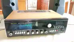
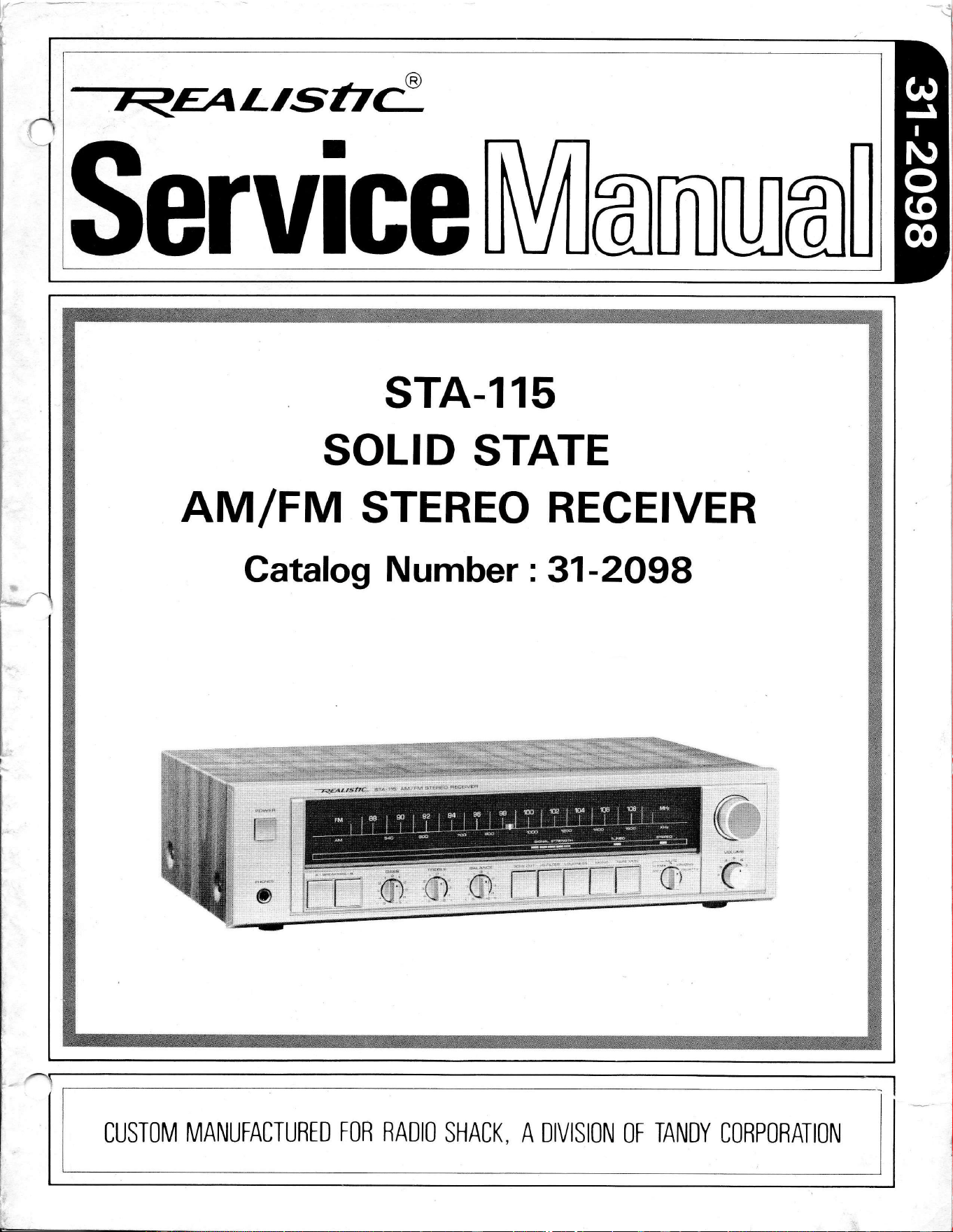
STA-115
SOLID
STATE
I
J
INT L
AM
IFM
STEREO
RECETVER
Catalog
Number :
31-2098
CUSTOM
MANUFACTUBED
FOR RADIO
SHACK,
A
DIVISION
t]F
TANDY
CORPORATION
PAGE
ELECTRICAL
PERFORMIANCE
SPECIFICATIONS
,,,,..
3-7
DISASSEMBLYINSTRUCTIONS.
B-9
BLOCKDIAGRAM..
...10
LEVEL DIAGRAM.
,.,..11
DIALSTRINGING
DIAGRAM.
,,.,.,.11
CTRCU|TDESCRIPTION
:.....
.12-13
OPERATIONAL CHECK
FOR
CIRCUITS
14
-
26
ALIGNME NT
I NSTRUCTIONS
27
-32
TROUBLESHOOTING...
33-35
TUNER
AUDIO
P.C.B,
(TOP
&
BOTTOM
VIEWS)
36
-
37
LEDP.C.B.(TOP&BOTTOMVIEWS).
.....
.38
SPEAKERSWTTCH
P.C.B.
(TOP&BOTTOM
VIEWS).
.......39
DIAL
POINTER P.C,B.
(TOP
& BOTTOM
VIEWS)
. . .
,39
WIRINGDIAGRAM
....40
EXPLODED
VIEW
41
_-
42
ELECTRICALPARTSLIST.
....43-55
EXPLODED VIEW
PARTS
LIST .
56
-_
57
TRANSISTOR
LEAD
IDENTIFICATION..
...58
IC LEAD
IDENTIFICATION &
INTERNAL DIAGRAM.
59
-
62
SCHEMATIC
DIAGRAM ,
.64-
65
PRODUCT,SAF'ETY
NOrteE'
',
''",
,,,ManV.eiectric-al,and,
rnech,anlcal"
'par.ts,,in
,this
ihassii
have specia|Ahaiaetefisties:,,:,f,heCe,e
harActef',.;
r
iiiiei,oitenlpiii1,unn,aiisld,
ain6,.15e
proiection,r61iqp6s6.
by' them
cannot necessarily
be obtained
..'brVr,Using.iep'iacement,
e:ompOnentsr,
rated,
toi:hi$her:,rvoltaggr,wattager,etc;,
.Fle-pJater:nent,pails,thal::
,
,conipronents,,naving,
sueS,,,isa,1u1s!,:6ie
ioentitiea,bV
er,,A
,!n
the sche.matic
diagram.,ahd,,the.nartii
list.
,..Beteieali+Oiaiing.,a,n17.of'tnese,ionrpoaenti.'reid:'16s
parts
list.i'n,this,ma"-u;l,,Careinjilfhi'tte
,
'.,sJnSiiiuta:rep'ljcrrnen,ttpiiii.,ihai.Ao
noi:traie,,ifle'sarne,safety
chaqacterlstics
as specified
in the
.)
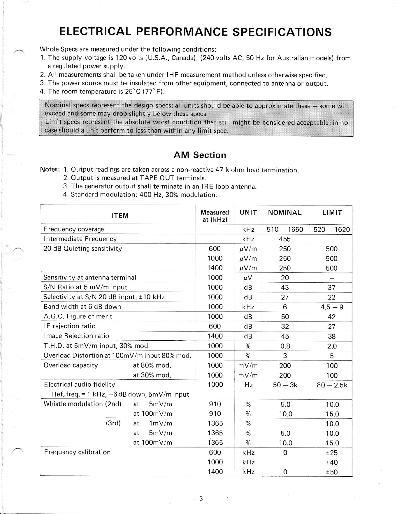
ELECTRICAL
PERFORMANCE
SPECIFICATIONS
Whole
Specs
are measured under the following
conditions:
1.
The supply
voltage
is 120volts
(U.S.A.,
Canada),
(240voltsAC,50
Hzfor
Australian models)
from
a regulated
power
supply.
2. All
measurements
shall
be taken under IHF
measurement method
unless otherwise
specified.
3.
The
power
source must
be
insulated
from other equipment, connected
to antenna
or output.
4.
The
room temperature
is
25'C
l77"Fl.
AM Section
Notes: 1.
Output
readings
are taken
across a non-reactive
47 k
ohm load termination.
2. Output is
measured
at TAPE
OUT terminals.
3.
The
generator
output
shall terminate
in an IRE loop
antenna.
4.
Standard
modulation:
4OO H2,30%
modulation.
ITEM
Measured
at
(kHz)
UNIT
NOMINAL LIMIT
Frequency coverage
kHz 510
-
1650
520
-
1620
I
ntermediate
Frequency
kHz
455
20 dB Ouieting
sensitivit.y
600
1000
1400
pV
lm
pV
lm
pY
lm
250
250
250
500
500
500
Sensitivity
at antenna terminal
1 000
pV
20
S/N Ratio
at
5
mV/m input
1 000 dB 43
37
Selectivity at
S/N 20
dB input,
r
10 kHz
1 000 dB
27 22
Band
width at
6
dB
down
1
000
kHz
6
4.5-9
A.G.C.
Figure
of merit
1 000 dB 50
42
I F
rejection
ratio
600
dB 32
27
lmaqe Reiection ratio
1400 dB
45 38
T.H.D.
at
5mV/m
input,30% mod.
1 000
o/
/o
0.8 2.O
Overload
Distortion
at
100mV/m
input
80%
mod.
1 000
o/
/o
3 5
Overload
capacity
at
80%
mod.
at 30% mod.
1 000
1 000
mV/m
mV/m
200
200
100
100
Electrical audio f idelity
Ref
..freq.
=
1 kHz,
-O
dB down,
5mV/m
input
1 000
Hz
50-3k
80
-
2.5k
Whistle modulation
(2nd)
at
SmV/m
at 100mV/m
(3rd)
at
1mV/m
at
5mV/m
at
100mV/m
910
910
o/
/o
o,/
/o
5.0
10.0
10.0
15.0
1
365
1 365
isos
o/
/o
o/
/o
o/
/o
5.0
10.0
10.0
10.0
15.0
Frequency calibration
600
1 000
1400
kHz
kHz
kHz
0
0
x25
x40
r50
-3
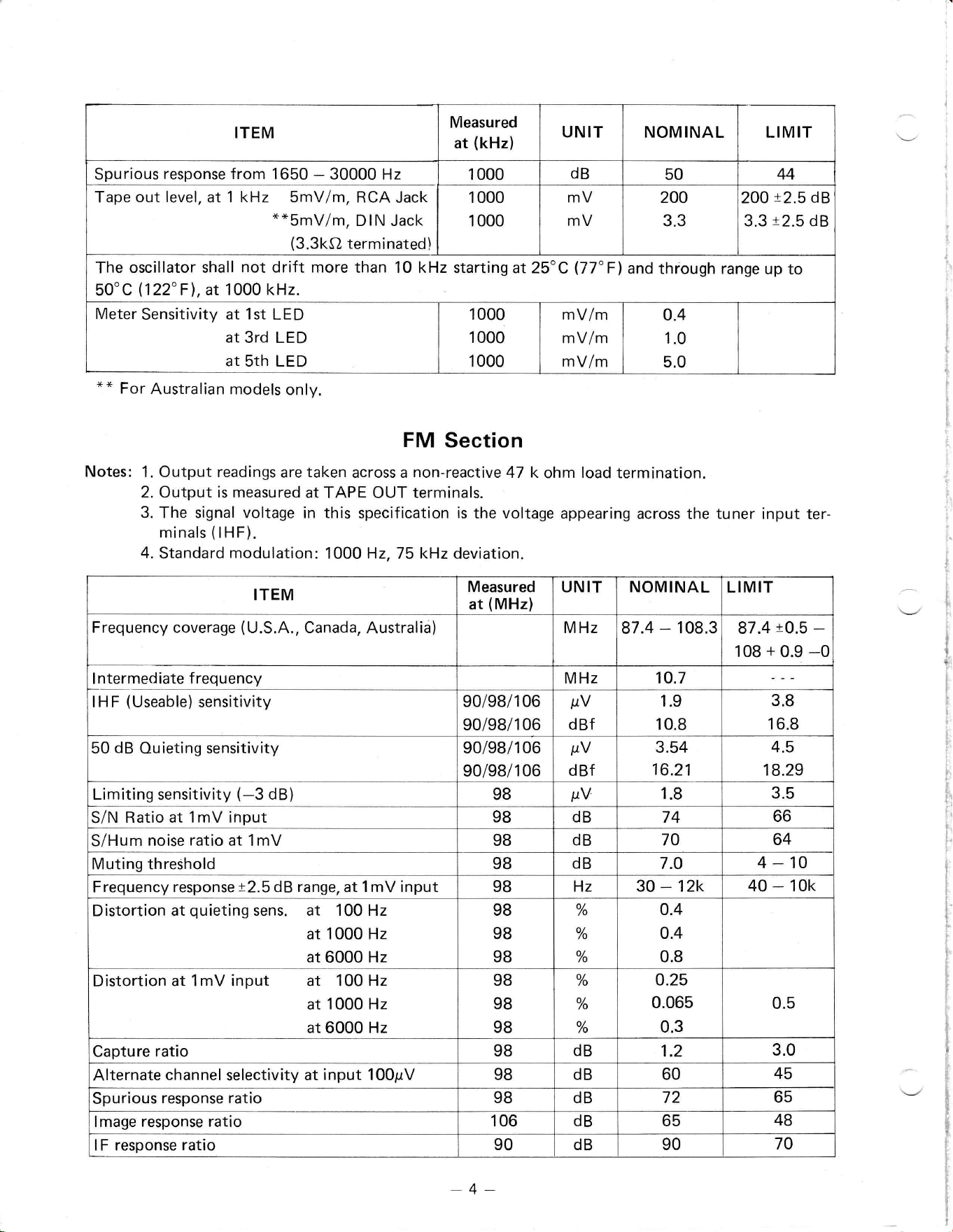
ITEM
Measured
at
(kHz)
UNIT NOMINAL
LIMIT
Spurious
response from
1650
-
30000
Hz
1 000
dB
50
44
Tape
out level,
at
1
kHz SmV/m, RCA
Jack
**5mV/m,
DIN Jack
(3.3kC}
terminated)
1
000
1 000
mV
mV
200
3.3
200
r2.5
dB
3.3
t2.5
63
The oscillator
shall
not drift more
than
10
kHz
starting at25"C
(77"F\and
thfough
range
up
to
50'C
(122"F\,
at 1000 kHz.
Meter
Sensitivity at
1st
LED
at 3rd LED
at sth LED
1000
1 000
1000
mV/m
mV/m
mV/m
o.4
1.0
5.0
**
For
Australian models
only.
FM
Section
Notes:
1. Output readings
are
taken
across
a
non-reactive
47 k
ohm load termination.
2. Output
is measured
at
TAPE OUT
terminals.
3. The signal voltage
in
this
specification
is
the voltage
appearing
across the
tuner
input
ter-
minals
(lHF).
4.
Standard
modulation:
1000
H2,75 kHz
deviation.
I
l
\-/
i
I
i
i
I
i,l
jl
i
I
(
1
T
I
t
i
)
1
ll
1t
N
I
I
l
\-/
t
l
i
t
I
I
I
IL
tl
il
l1
il
il
rj
i
I
t.l
I
t1
rl
I]
I
il
dt
$l
\-/
tl
tl
[1
t
t
t
_l
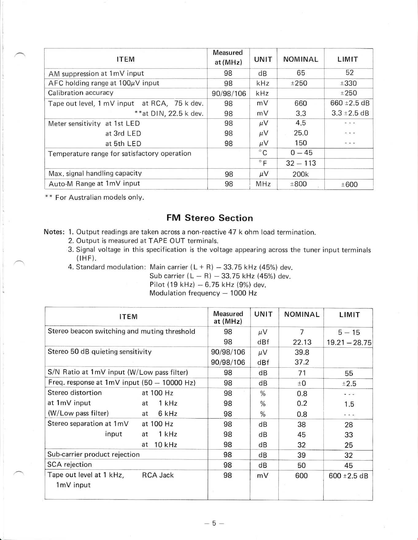
ITEM
Measured
at
(MHz)
UNIT
NOMINAL LIMIT
Frequency coverage
(U.S.A.,
Canada,
Australia)
MHz
87
.4
-
108.3
87.4
tO.5
-
108
+
0.9
-0
ntermediate frequency MHz 10.7
HF
(Useable)
sensitivity 90/98/1
06
90/98/106
pV
dBf
1.9
10.8
3.8
16.8
50
dB
Ouieting sensitivity 90/98/106
90/98/106
pV
dBf
3.54
16.21
4.5
18.29
Limiting sensitivity
(-3
dB)
98
pV
1.8
3.5
S/N
Ratio at 1mV input 98
dB
74
66
S/Hum
noise
ratio
at 1mV 98
dB
70 64
Muting threShold
98
dB
7.O
4-10
Frequency response
t2.5
dB
range,
at
1mV input 98
Hz
30
-
12k
40
-
10k
Distortion at
quieting
sens.
at 100 Hz
at
'1000
Hz
at
6000 Hz
98
98
98
%
o/
/o
o/
/o
o.4
o.4
0.8
Distortion
at 1mV input at 100 Hz
at 1000 Hz
at 6000
Hz
98
98
98
o/
/o
o/
lo
o/
/o
o.25
0.065
0.3
0.5
Capture
ratio
98
dB
1.2
3.0
Alternate
channel
selectivity
at input 100pV 98
dB
60
45
Spurious
response ratio 98 dB
72
65
lmage
response ratio
106
dB 65
48
lF response ratio
90
dB 90 70
-4-
I
FM
Stereo
Section
Notes:
l.Outputreadingsaretakenacrossanon-reactive4T kohmloadtermination.
2.
Output
is
measured
at TAPE
OUT
terminals.
3. Signal
voltage in
this specification is the voltage
appearing across the tuner
input terminals
flHF).
4.
Standard
modulation: Main
carrier
(L+
R)
-33.75
kHz
(45%)
dev.
Sub
carrier
(L
-
R)
-
33.75 kHz
(45%)
dev.
Pitot
(19
kHz)
-
6.75
kHz
(9%)
dev.
Modulation
frequency
-
1000 Hz
ITEM
Measured
at
(MHz)
UNIT
NOMINAL LIMIT
AM suppression
at 1mV
inPut 9B dB
65
52
AFC holding
range at 100prV input
98
kHz
x250 t330
Calibration
accuracy
90/98/1 06
kHz
t25O
Tape
out level, 1 mV input
at RCA, 75 k dev.
**at
Dl
N,
22.5
k dev.
98
98
mV
mV
660
3.3
660
t2.5
dB
3.3
t2.5
dB
Meter
sensitivity
at 1st LE D
at 3rd LED
at Sth LED
9B
98
9B
pV
pV
pV
4.5
25.O
150
Temperature
range
for
satisfactory
operation
"c
0-45
OF
32
-
113
Max. signal
handling
capacity
9B
pV
200k
Auto-M
Range
at
1mV
inPut
98
MHz
tB00
t600
*
*
For Australian
models
only.
ITEM
Measured
at
(MHz)
UNIT
NOMINAL
LIMIT
Stereo
beacon
switching
and muting
threshold
98
9B
pV
dBf
7
22.13
5
-
15
19.21
-28.75
Stereo 50
dB
quieting
sensitivity
90/98/106
e0i98l1
06
pV
dBf
39.8
37.2
S/N
Ratio at 1mV
input
(W/Low
pass
filter)
9B
dB
71
55
Freq. response
at 1mV
input
(50
-
10000 Hz)
98 dB
t0
t2.5
Stereo
distortion
at
100
Hz
at
1mV input
at 1 kHz
(WlLow
pass
filter)
at
6 kHz
98
98
9B
%
o/
/o
o/
/o
0.8
0.2
0.8
1.5
Stereo separation
at 1mV
at 100
Hz
input
at
1
kHz
at
10
kHz
9B
9B
98
dB
dB
dB
38
45
32
28
33
25
Sub-carrier
product
rejection
98 dB
39
32
SCA
rejection
98 dB
50 45
Tape
out level
at 1 kHz,
RCA Jack
1mV
input
98 mV
600 60012.5 dB
-5-
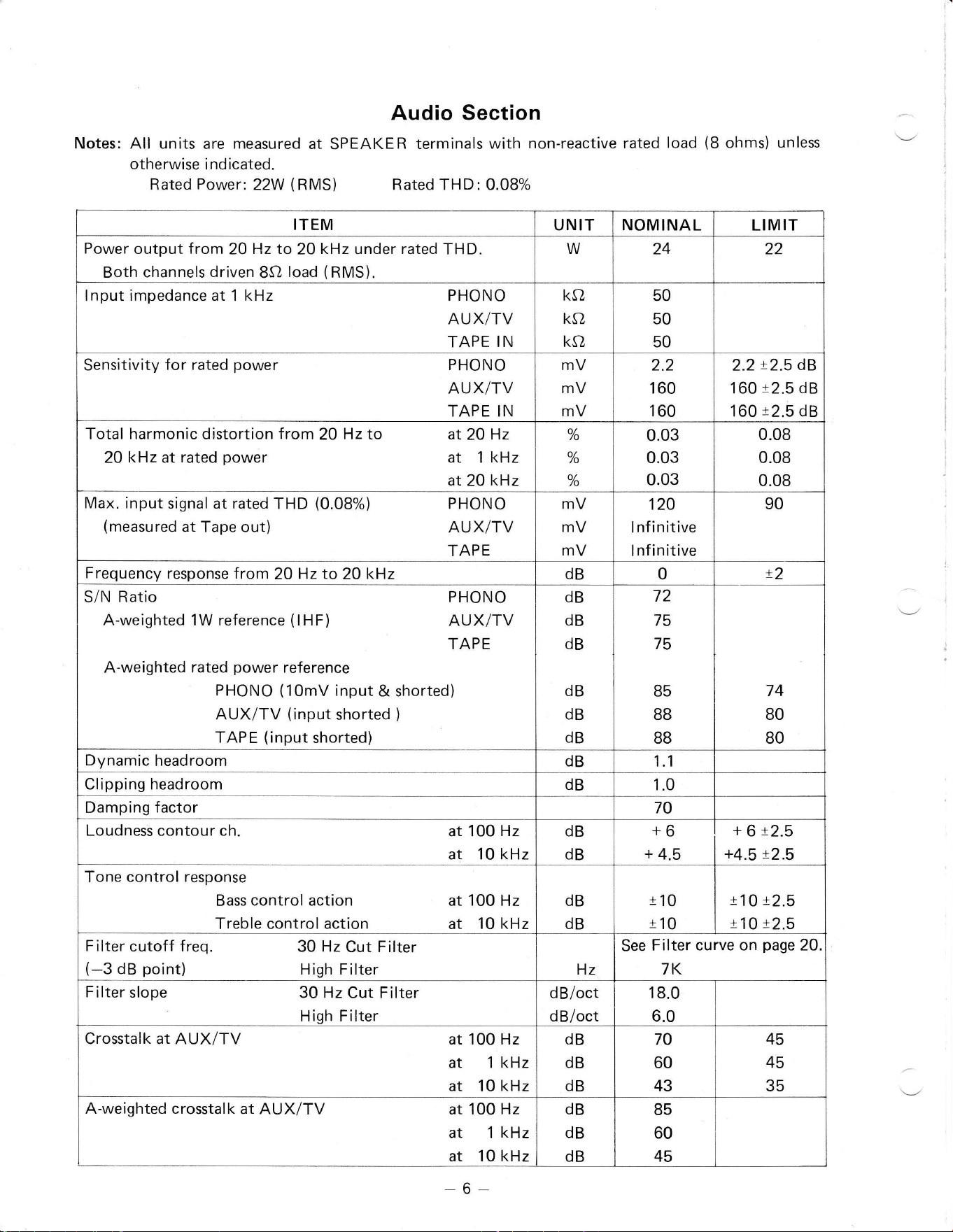
Audio Section
Notes: All units
are
measured
at
SPEAKER
terminals
with
non-reactive rated
load
(B
ohms)
unless
\--l
otherwise
indicated.
Rated
Power:
22W
(RMS)
Rated THD: 0.08%
ITEM
UNIT NOMINAL
LIMIT
Power output from
20
Hz to
20
kHz
under
rated
THD.
Both
channels
driven
8Sl
load
(RMS).
W
24 22
lnput
impedance at 1 kHz PHONO
AUX/TV
TAPE
IN
ke,
ko
ko
50
50
50
Sensitivity
for rated
power
PHONO
AUX/TV
TAPE IN
mV
mV
mV
2.2
160
160
2.2
x2.5
dB
160
r2.5
dB
16012.5 dB
Total harmonic distortion
from
20
Hzto
at20 Hz
2OkHz at
rated
power
at 1
kHz
at
20
kHz
o/
/o
o/
/o
o/
/o
0.03
0.0s
0.03
0.08
0.08
0.08
Max. input
signal at rated
THD
(0.08%)
PHONO
(measured
at
Tape
out)
AUX/TV
TAPE
mV
mV
mV
120
lnfinitive
I
nf initive
90
Frequency
response from
20
Hz to
20 kHz dB
0
t2
S/N Ratio PHONO
A-weighted 1W reference
(lHF)
AUX/TV
TAPE
A-weighted rated
power
reference
PHONO
(1OmV
input
& shorted)
AUX/TV
(input
shorted
)
TAPE
(input
shorted)
dB
dB
dB
dB
dB
dB
72
75
75
85
BB
8B
74
80
80
Dynamic
headroom
dB
1.1
Clipping headroom
dB
1.0
Damping
factor
70
Loudness
contour ch.
at 100
Hz
at 10 kHz
dB
dB
+6
+
4.5
+
6
12.5
+4.5 !2.5
Tone control
response
Bass
control action
at
100
Hz
Treble control
action
at 10
kHz
dB
dB
t10
t10
t1O x2.5
t
10
t2.5
Filter cutoff freq.
30 Hz
Cut
Filter
(-3
dB
point)
High
Filter Hz
See
Filter
curve on
page
20.
7K
Filter
slope
30 Hz
Cut
Filter
Hioh Filter
dB/oct
dB/oct
18.0
6.0
Crosstalk at AUX/TV
at 100 Hz
at 1 kHz
at
10
kHz
dB
dB
dB
70
60
43
45
45
35
A-weighted crosstalk
at AUX/TV
at 100 Hz
at 1 kHz
at
10 kHz
dB
dB
dB
85
60
45
-6-
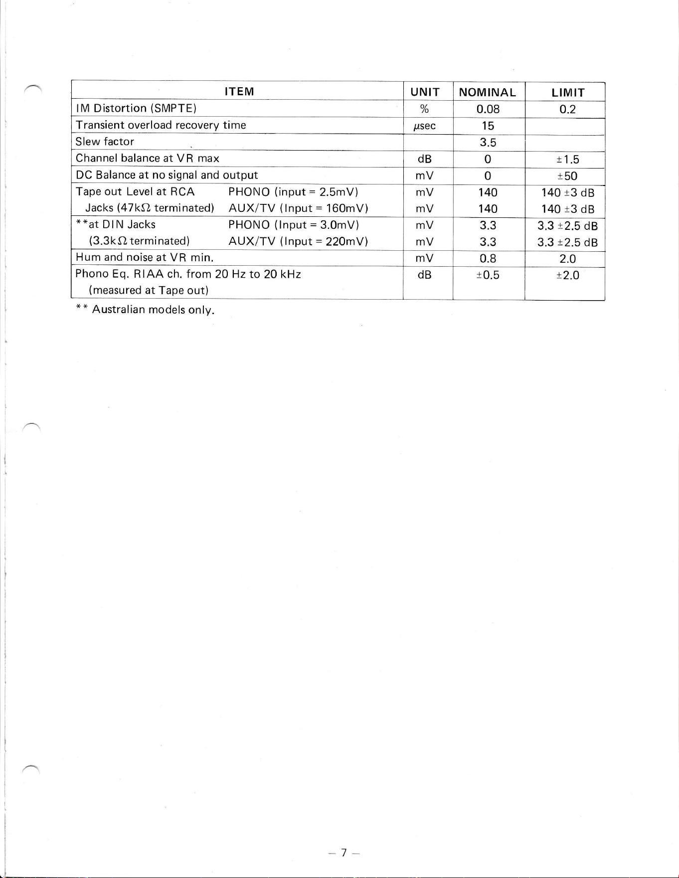
ITEM
UNIT
NOMINAL
LIMIT
lM Distortion
(SMPTE)
o/
/o
0.08
o.2
Transient overload recovery time
psec
15
Slew factor
3.5
Channel balance at V
R
max
dB
0
t
1.5
DC
Balance at no signal and output
mV
0
t50
Tape
out
Level
at
RCA PHONO
(input
=
2.5mV)
Jacks
(47kQ
terminated)
AUX/TV
(lnput
=
160mV)
mV
mV
140
140
140
13
dB
140
t3
dB
""at
DIN
Jacks PHONO
(lnput
=
3.0mV)
(3.3kOterminated)
AUX/TV
(lnput=Z2OmYl
mV
mV
3.3
3.3
3.3
t2.5
dB
3.3
t2.5
dB
Hum and noise
at
VR min.
mV
0.8
2.O
Phono
Eq. H IAA ch.
from
2A
Hz to
20
k
Hz
(measured
at
Tape
out)
dB
10.5
t2.O
**
Australian
models only.
-7
-
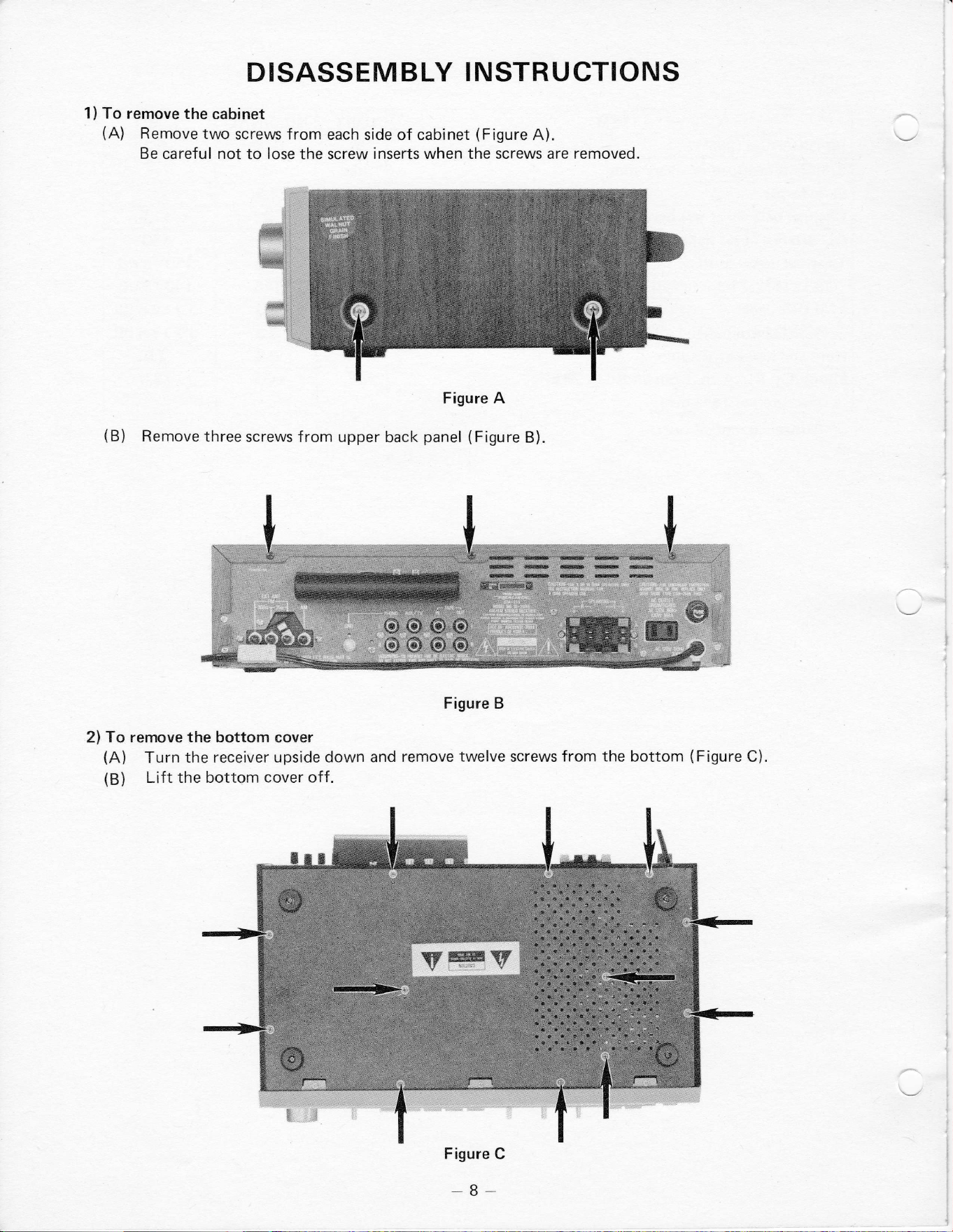
DISASSEM BLY
I NSTRUCTIONS
1) To remove
the
cabinet
(A)
Remove
two
screws from
each side of cabinet
(Figure
A).
Be careful not
to
lose
the screw
inserts when the screws are
removed.
Figure A
Remove three
screws
from upper back
panel
(Figure
B).
(B)
lt:i
t::t:L:l
l,t:t:t 1 i ! :
t:t:i;!l;i i
:.
_'
:.:a
:..
4:
:;t:l::ttt:i:.ffi
Figure B
2)
To remove the bottom
cover
(A)
Turn
the receiver upside
down and
remove
twelve
screws
from the bottom
(Figure
C).
(B)
Lift the bottom
cover
off .
i,.,..
Nir'.'
'Nil,.
ia.1.,l,'il
$Ni;rl
s$.4r.
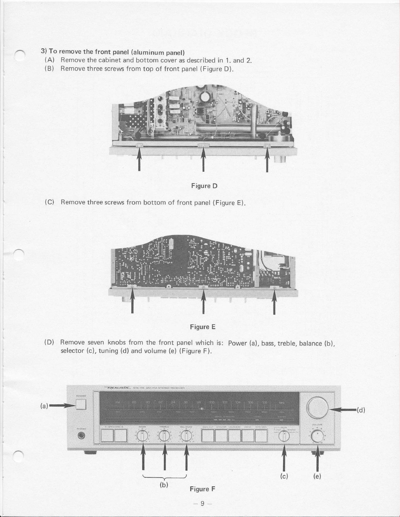
3)
To
remove
the front panel
(aluminum
panel)
(A)
Remove
the cabinet
and bottom cover
as described in
1. and 2.
(B)
Remove three
screltrs from
top of front
panel
(Figure
D).
Figure
D
(C)
Remove
three screws from
bottom
of front
panel
(Figure
E).
(D)
Remove
seven knobs
from the front
selector
(c),
tuning
(d)
and volume
(e)
Figure
E
panel
which is:
Power
(a),
bass,
treble, balance
(b),
(Figure
F).
\---_____Y__-__J
(b)
Figure F
9-
:ariee4g$Ae-
.$ta-lr* tlrrrM:qtqae':e€*rvrn
G_
P;
6@
J
LlJ
z
z
-
o
F
Lr
lrJ
J
o
o
o,
E
o
a
J
td
z
z
-
o
F
I
(,
(ts
2H
F-
-o
=R
=E
uts
E
u
Eo!
Iu
--
:9cVo
,ou=o
^z)o
--
5=9i-
za<)
i
"o
F
]E
UU
Sf.
3tr
Xo
=x
=9
L-
)Ei
g6;
uo'
n
dE3
Hze
F3,
3E3
<ze
6O
>
c
==
Ze
9o
s{8
! oF
H=5
FiN
U
J=
o >=
o
:
E
luu
!e
=l
J<
\E
ro
=l
LO
J
<E
zo )
0Fo
6*s
u=o
tao
ix
ZY
=<
oo
oE
UZ
J*
o
-
uI
-drr
OU;
6b;
=@
G
P_
a*o
sx=
6-3
tIo
o<
JF
z
^-z
a
'."f
o
"'1
ts
@
-=
o
r
r
E-
<o
LN
=r
L
a
=
P;
l>
EE
=F
Io
E9
Etr
IF
5?
Eg
2E
o
L
\J
zz
oo
la
L\
Eo
>0
E
UIL
@F€
5Ia
uo
5
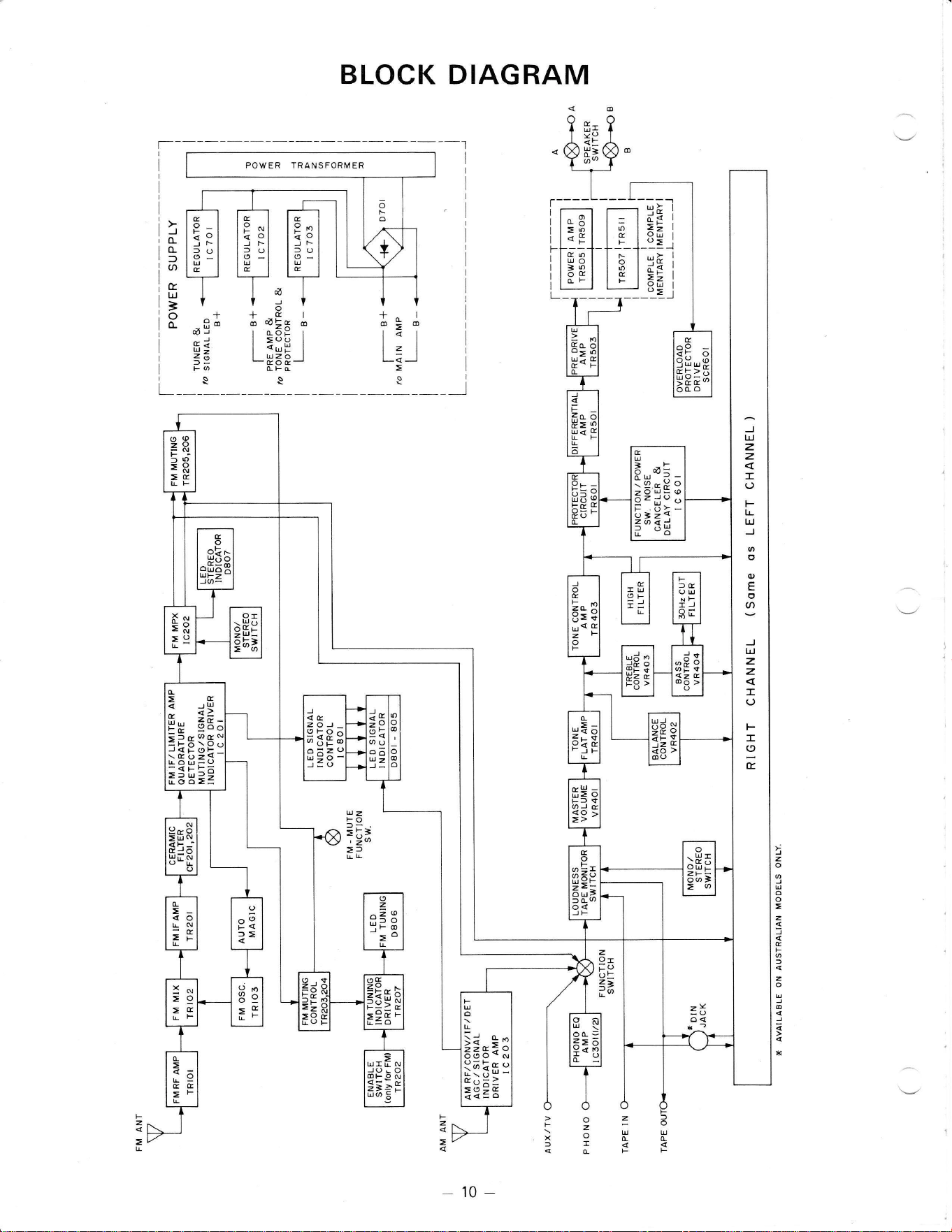
BLOCK
DIAGRAM
I
I
I
I
I
I
L
I
I
___l
i*Ld[rHM
ia I I
-
I-
----l--1
ig
+
+
:
+ + +
ig
-s*
**ExI tgJ
i
ooJ
I
Go;
I I a I
i _J |
=ao
I I I
I
iE
L[x;-]
L=-.1
I Fo [Fr
=
l"6o
uz
FO
l-
=l:=
'Za
=f
LL
-
z
o
J
6
o
=
z
s
)
c
F
z
o
J
6
a
*
z
9r
LO
bF
==
ia
F
z
E
E
POWER TRANSFORMER
E
o_
ts^
JN
lo
u
E
g
9o
ko
JF
fo
0-
U
&
e
9o
JN
lo
0-
U
E
10
rTAPE IN
I
I
F
l
L
AUX,/
TV
z
T
LpHotto
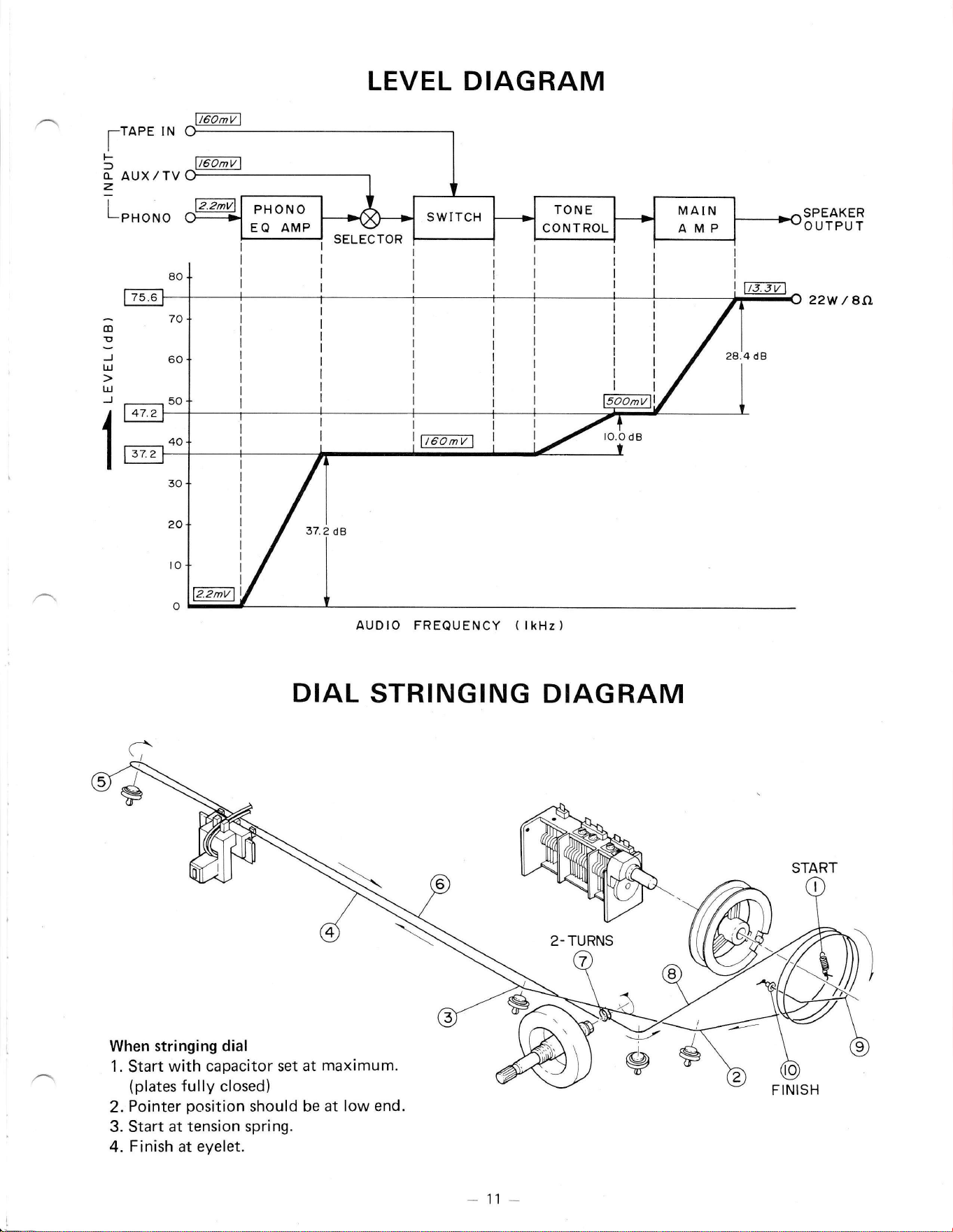
When stringing
dial
1.
Start
with
capacitor set
at
maximum.
(plates
fully
closed)
2.
Pointer
position
should be
at low end.
3. Start
at tension spring.
4.
Finish at eyelet.
LEVEL DIAGRAM
SPEAKER
O UTPU T
22w
/ AO
c)
3
)
UJ
UJ
)
70
60
50
28.4 dB
to.odB
30
20
to
o
37.2 dB
DIAL
STRINGING DIAGRAM
PHONO
EQ
AMP
SWITCH
TONE
CONTROL
MAIN
AMP
AUDIO FREQUENCY
(
lkHz
)
-
11
*
Y]
@tr
-u-
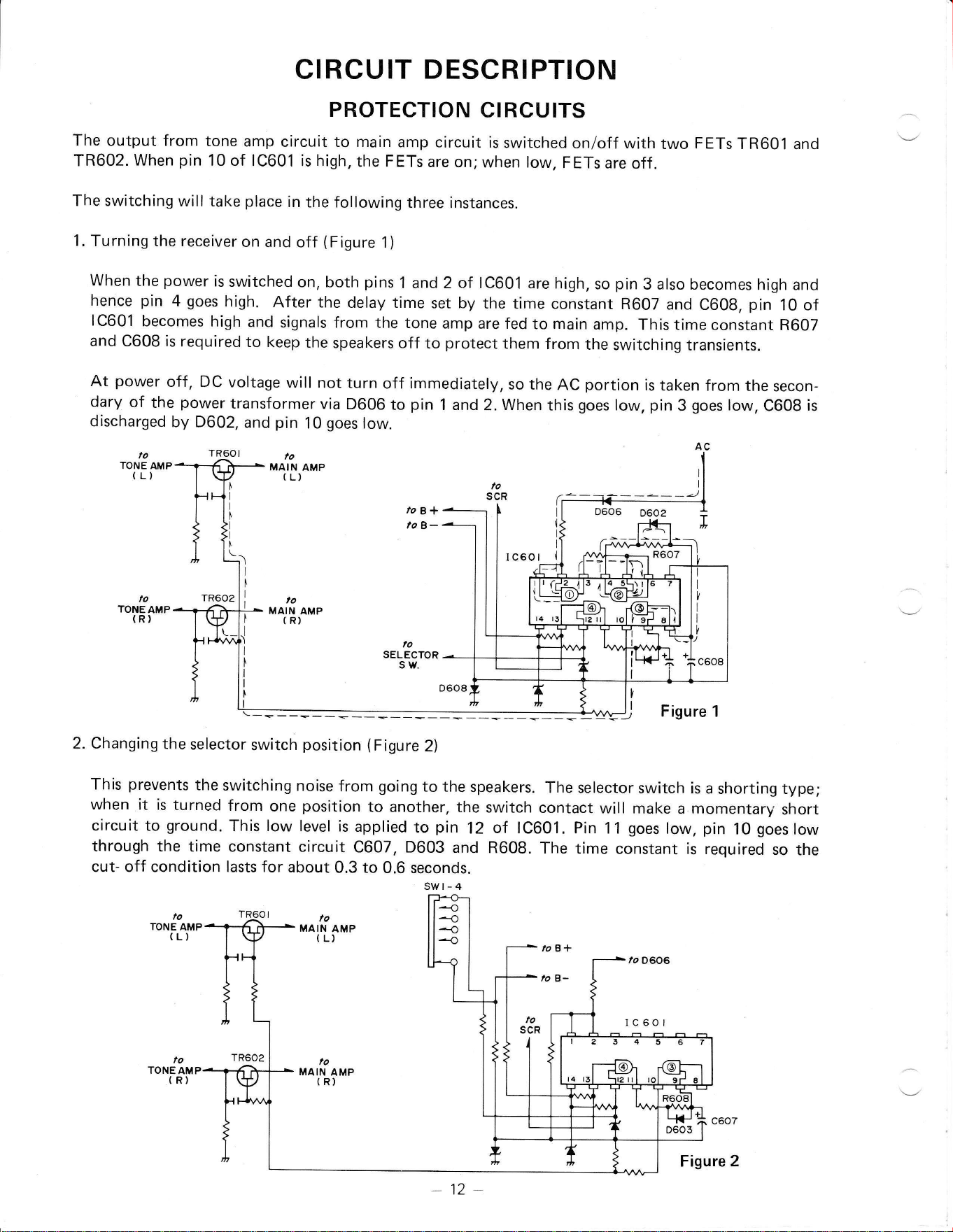
CIRCUIT
DESCRIPTION
PROTECTION
CIRCUITS
The output from
tone
amp
circuit to main
amp circuit
isswitched
on/off
with
two
FETsTR601
and
TR602.
When
pin
10 of 1C601 is high,
the FETs
are
on; when low,
FETs
are off.
The switching
will take
place
in
the following
three
instances.
1
. Tu
rn
ing the receiver
on
and off
(
F igure
1
)
When
the
power
is
switched
on, both
pins
1 and 2
of
1C601 are
high,
so
pin
3 also becomes
high
and
hence
pin
4
goes
high.
After the
delay time
set
by
the
time constant
R607
and
C608,
pin
10 of
1C601
becomes
high
and
signals
from the tone
amp
are fed
to
main
amp.
This time
constant R607
and C608 is
required
to
keep
the
speakers
off to
protect
them
from
the
switching
transients.
At
power
off, DC
voltage
will not
turn
off
immediately,
so the
AC
portion
is
taken
from the
secon-
dary
of
the
power
transformer
via
D606
to
pin
1 and
2.
When
this
goes
low,
pin
3
goes
low,
C608
is
discharged
by D602,
and
pin
10
goes
low.
lo
TONE
AMP
(L)
lo
MAIN
AMP
(
L)
A
!
I
I
lo
B+
to B-
D6O6
D6O2
Figure 1
2. Changing
the
selector
switch
position
(Figure
2)
This
prevents
the
switching
noise
from
going
to
the speakers.
The selector
switch is
a shorting type;
when
it is turned
from
one
position
to another,
the
switch
contact
will
make a momentary
short
circuit to
ground.
This low
level is
applied
to
pin
12
of
1C601. Pin 11
goes
low,
pin
10
goes
low
through the
time constant
circuit
C607, D603
and
R608.
The
time constant
is required
so
the
cut- off condition lasts for
about
0.3
to 0.6 seconds.
,o
MAIN
AMP
(R)
-12-
3.
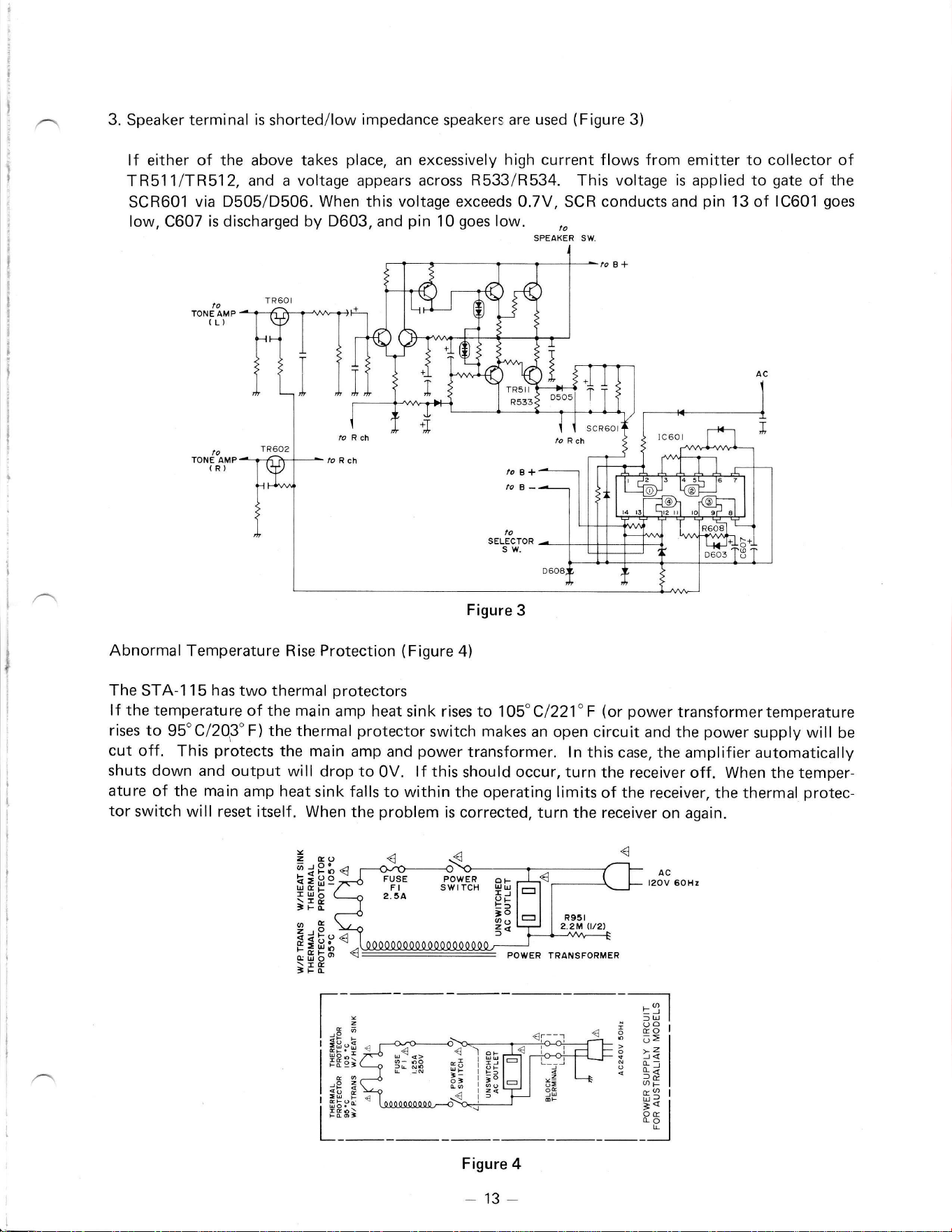
Speaker terminal
is
shorted/low
impedance
speakers
are used
(Figure
3)
lf either of the above takes
place,
an
excessively
high
current flows from
emitter to
collector
of
TR511/TR512,
and
a voltage appears across
R533/R534.
This
voltage is
applied to
gate
of
the
SCR601
via D505/D506.
When
this
voltage
exceeds 0.7V, SCR conductsand
pin
13of 1C601
goes
low,
C607
is discharged by
D603,
and
pin
10
goes
low.
to
TONE AMP
(R)
Abnormal
Temperature Rise
Protection
(Figure
4)
The STA-1 15
has
two thermal
protectors
lf the
temperature
of the
main
amp
heat
sink rises to
1O5"C1221"
F
(or
power
transformertemperature
rises to
95"C/20,3'F)
the
thermal
protector
switch
makes
an open circuit
and the
power
supply
will
be
cut off.
This
protects
the main
amp and
power
transformer. ln this
case, the amplifier
automatically
shuts down and
output
will dropto
0V. lf this
should
occur,turn
the
receiveroff. When
thetemper-
ature of the main
amp
heat
sink falls
to within the
operating limits
of
the
receiver,
the thermal
protec-
tor
switch will reset
itself. When the
problem
is corrected,
turn
the receiver
on
again.
AC
l2OV
6OHz
Figure
4
-13-
Y
zE
6r9
tsEE
IU;\
iIE
qE
2t9
E=H
rGts
cuo
>EE
-;,t
lul
oo ;
Eol
6>l
\il
[- I
s#
I
atl
ftq
I
a-i I
or I
[o
I
__l
I
z
a
I
,
z
F
d
)
I
i
38"
I EFs
t"
l*E"
t-
i
i
I
:
rt Rch
/o Rch
loRch
Figure
3
OF
UU
IJ
9F
El
=o
2e
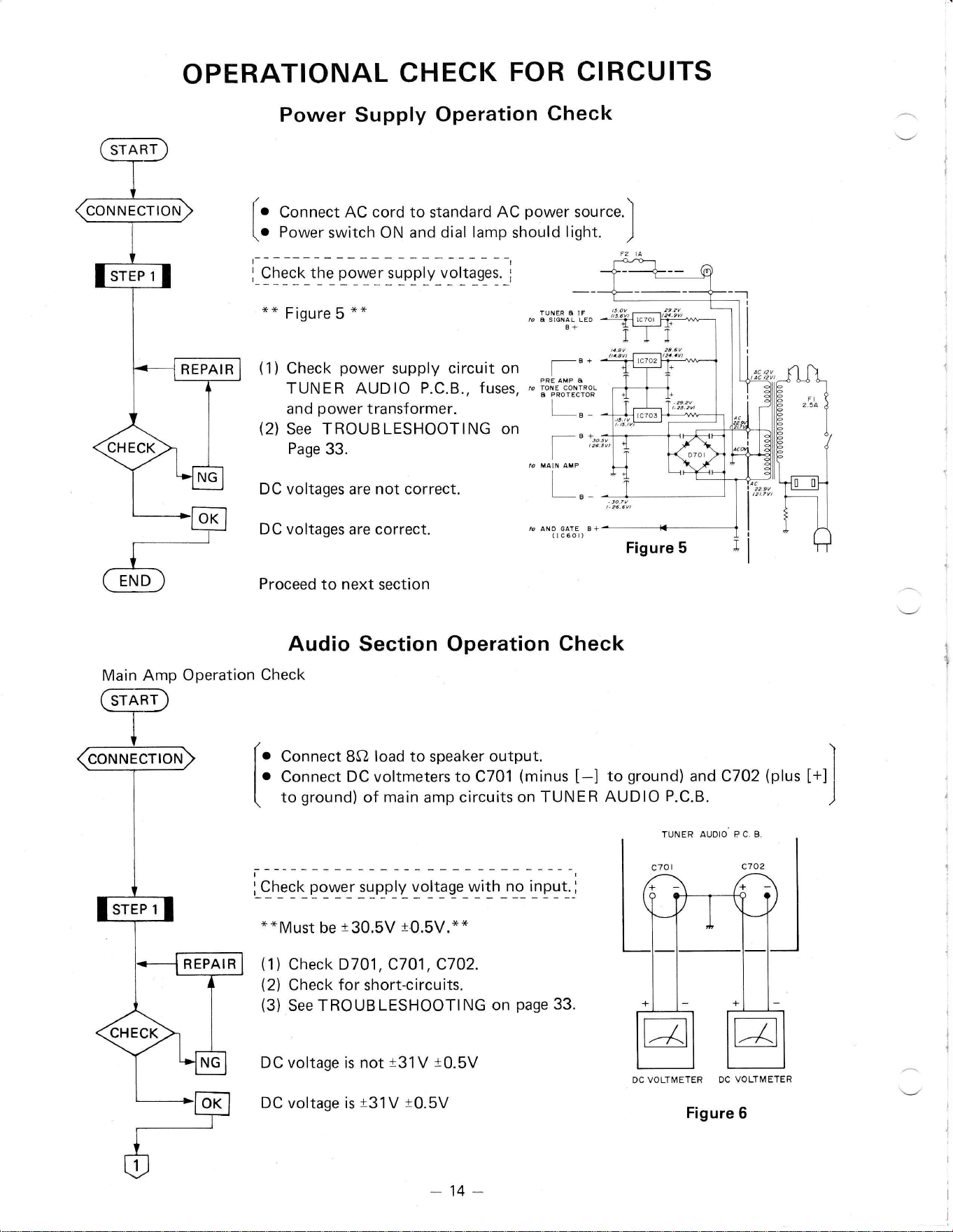
OPERATIONAL
CHECK
FOR CIRCUITS
Power Supply
Operation
Check
[.
aonn."t AC
cord to
standard
AC
power
rorr...l
(o Power
switch ON and
dial lamp
should
light.
)
(1)
Check
power
supply
circuit on
TUNER AUDIO P.C.B.,
fuses,
and
power
transformer.
(2)
See TROUBLESHOOTING
on
Page
33.
DC voltages
are
not correct.
DC
voltages
are correct.
START
CONNECTION
REPAIR
-B+
+
!
ro
TONE
CONTROL
& PROTECTOR
I
B-
L"_
Proceed
to
next
section
Audio Section Operation Check
(.
Conn..t BO
load to
speaker
output.
|
.
Connu.t
DC voltmeters to C701
(minus
[-]
(
to
ground)
of
main
amp circuits
on TUNER
i----
i_c_[e9(qo_ryeMp_p.!y_yo]t_ao_e_vyiLh_1q'IPyt_r
**Must
be
t30.5V
IO.SV."*
(1)
Check D701, C701, C702.
(2)
Check for short-circuits.
(3)
See
T
RO
UB
LESHOOTI NG on
page
33.
DC voltage is not
t31V t0.5V
DC voltage is
t31V t0.5V
Figure 5
702
(
PC.B.
c702
DC VOLTMETER DC
VOLTMETER
Figure
6
)andC
C.B.
ER AUDIO
nd
P.
TUI\
70t
UNE
)l
olm
t*f]
CONNECTION
STEP
1
:CK
REP AIR
CH
t\
LJ
OK
1
to
gr
AUD
-14-
iAdjust
DC balance
and
idling
current.
r
l_s9e_4!r_GryV_ENIL\sIEqqr_r9rys_gLqage_?B_._i
[.
Conn.., DC
voltmeter
to
pin
11
(L)
or
pin
12
(R)l
(
and GROUND of TUNER
AUDIO P.
C. B.
)
DC VOLIMETER
Figure
7
i_.1.:f
!iplqry:"_t_r_._*lrgs:
g,
L_.1J n .r,rr,".i"r.pr.
,"_'li1a
."]
*"
within
t50mV.*"
(1)CheckTR501 (L)
orTR502
(R).
DC voltage
over
t50mV
DC
voltage
within
t50mV
(:
[.
Conn."t DC voltmeter
to R531
(L
ch)
or R532
(R
ch)J
Figure
8
icrrect<
the
idling
"urlniot
*rr"
lrnp
*i.1
""
i"p;.-
-
tCheck
the DC voltage
across emitter resistor R529
(R531)
(L
ch)
and
lnsso
(Rb32) (R
ch).
**should
be
2.35mV
+4.71-1.88mV.
*"
(1)
Check the value
of
R519
(L
ch)
and
R520
(R
ch).
IFor
Australian models, adjust
VR 501(L
ch) and VR
502
(R
ch).]
(2)
Check
the
bias
circuit
of D501,
D503
(L
ch) and/or D502,
D504
(R
ch).
(3)
Check TR503
(L
ch)
and TR504
(R
ch).
(4)
Check
TR501,
(L
ch) and
TR502
(R
ch).
(5)
Check
for
short-circuits
on TUNER
AUDIO
P.C.B.
DC
voltage
is
above 7.05mV or below 0.47mV.
DC voltage is
2.35mV
+4.71-1.BBmV.
'i
I
I
I
I
I
I
ADJUSTMENT
REPAIR
-
15
-
CONNECTION
REPAIR
ADJUSTMENT
R EPAIR
CHECK
(.
l.
l.
t
Connect
oscilloscope and
V.T.V.M. to speaker
terminal.
'l
Connect
8O
load to
speaker
output.
]
Connect
audio osc.
to
input of
main
amp
circuit: C501s
plus
(+)
side
(L),1
and/or
C502s
plus
(+)
side
(R)
|
lnput should be 500mV
and output should
be 13.3V
(at
1
kHz)
)
OSCILLOSCOPE VIV.M
auDro osc.
TUNER,AUDTO
PC.3
en LoAo
Figure 9
t--------------l
l-c_ry
9 L l"l 1yl]l.l
rl.3
l_c I
i
p
p
i n_s
_o
f
9 lt! lt :,! 1u L
y1:
$i
q g
_i
*
*
lnput
level
should be about 600mV
to
1.0V.*"
(1)
Check TR501, 503, 505, 509
(L)
and TR502,
504, 506, 510
(R),
(2)
Check
STEP 2
and
STEP
3.
(3)
Check
main
amp.
circuits.
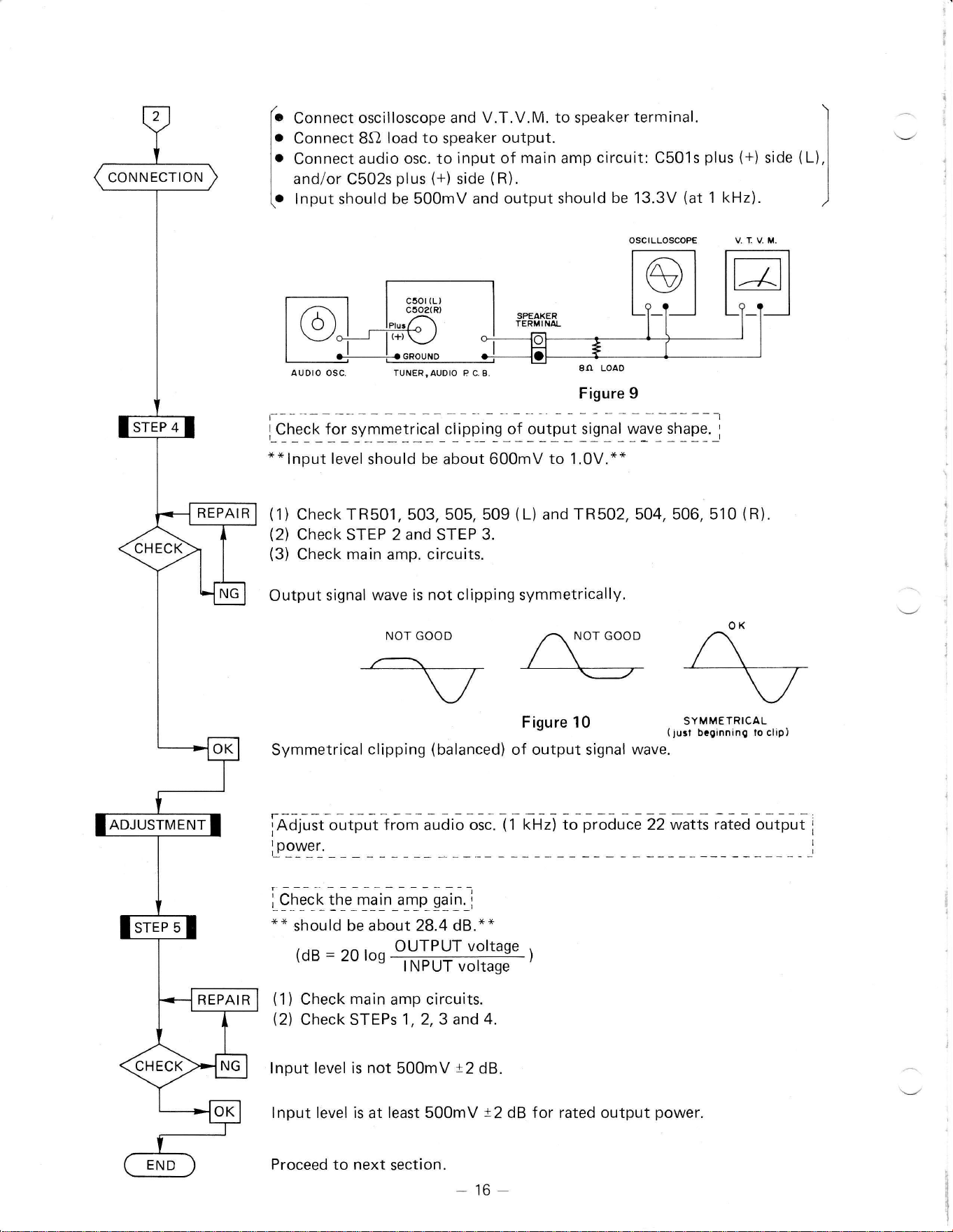
Output
signal
wave is not
clipping
symmetrically.
NOT
GOOD
^v
Figure 10
Symmetrical
clipping
(balanced)
of output signal
iAJ;rit
"riprtlA,
*oio oiC.IItnri
SYMMETRICAL
(jusi
bcginninO
to clip)
WAVC.
to
produce
22 watts
rated
output
iQn* t,f"
".1i"
.*n_Sq.q,
"*
should
be about 28.4 dB.*"
OUTPUT voltaqe
(dB
=
2u
ros
rNpurr *rtE-')
(1)
Check
main
amp
circuits.
(2)
CheckSTEPs
1,2,3 and4.
lnput
level is not
500mV
l2
dB.
lnput level is
at
least 500mV
t2dB
for rated output
power.
Proceed
to next
section.
-16
(+)
Preamp
Operation
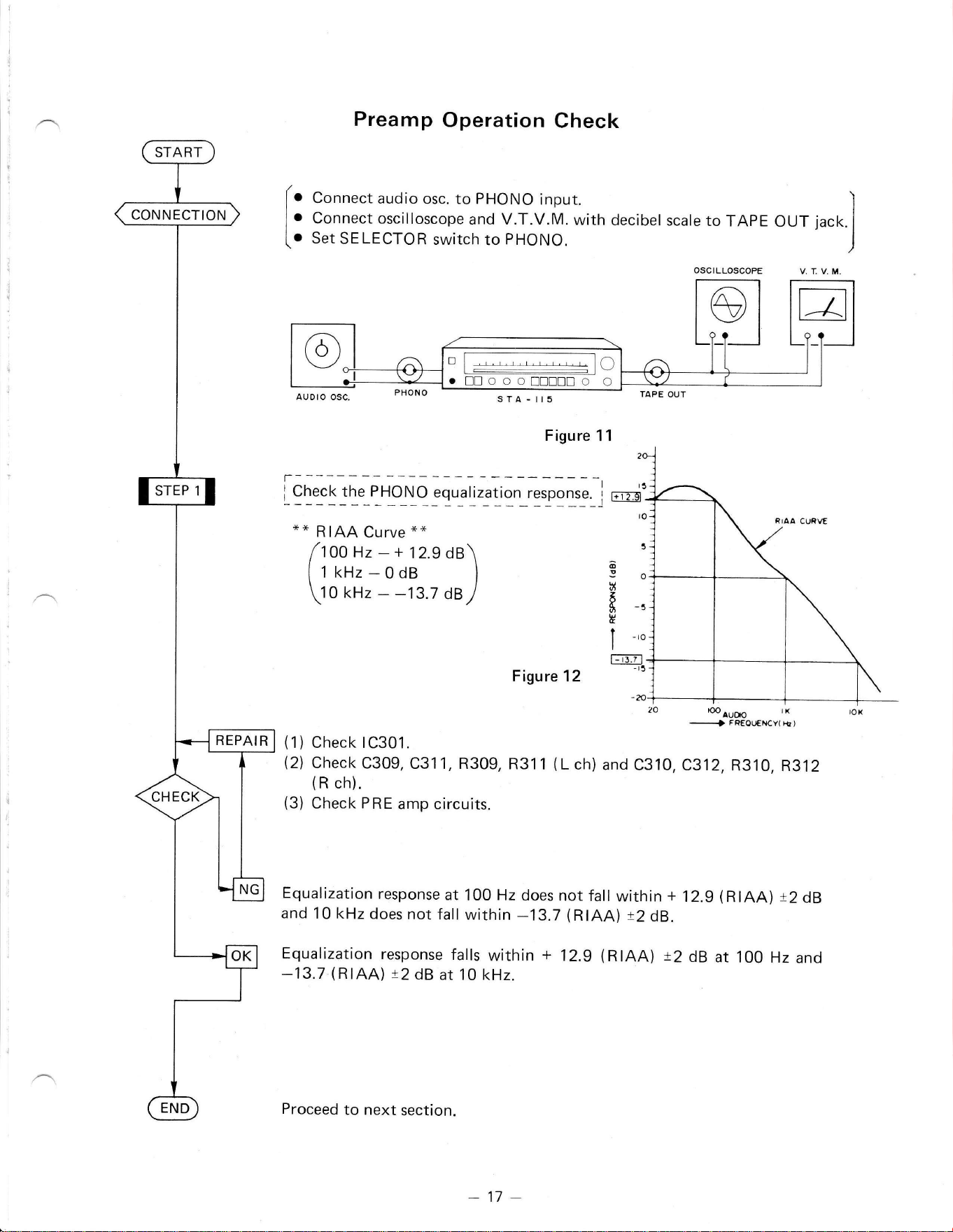
Check
Connect
audio
osc. to PHONO
input.
connect
oscilloscope
and
V.T.V.M.
with
decibel
scale
to
TApE
oUT
jack.
Set
SE
LECTOR
switch
to
pHONO.
Figure 11
(.
l.
[.
"*
RIAA
Curve
**
[loo
n,
-
+
12.9
dB\
(
t
r.Hr-odB
)
\r
o
rHz
-
-13.7
dB
)
(1)
(21
(3)
Figure 12
2o ,@
Auoo
I x
Check
1C301.
Check
C309,
C31 1,
R309, R31
1
(
L ch)
and
C310,
C512, R310,
R31 2
(R
ch).
Check
PRE
amp
circuits.
Equalization
response
at 100 Hz
does not
fallwithin
+
12.g
(RIAA)
!2dB
and 10 kHz
does not
fall
within
-13.7
(RtAA)
t2
dB.
Equalization
response
falls
within
+
12.9
(RIAA)
12
dB
at
100
Hz
and
-13.7
(RIAA)
!2dB
at 10 kHz.
OSCILLOSCOPE
DtroooD!trtrtro
o
T----
L 9 !1"5
_tl'_P_lolo_
:.
g,_u
!.3!
gy9T9
11.:
]
REPAIR
Proceed
to next
section.
-11
-
CONNECTION
Tone Control
Operation
Check
Connect audio
osc.
to AUX/TV input
jack.
Connect
oscilloscope and V.T.V.M. to
speaker
terminal.
Connect BO load to speaker output.
Set SELECTOR switch to AUX/TV
position.
TAPE MONITOR:
OFF
MONO
switch:
STEREO
LOUDNESS:
OF
F
a
a
a
a
o
a
a
oscrlloscoPE v_ T- v. M.
auDr o osc.
f---
--
iCfreck BASS action at
100
Hz.
i
t_
_
_
-
_
_ _ ___t
**
TONE CONTROL Curve"*
Figure
14
roo rk
*
AUDIO FREQUENCY
(Hz)
(1)
Check bass
control circuit
on TUNER
AUDIO
P.C.B.
(2)
See
TROUBLESHOOTING
on
page
35.
Frequency response does
not
fall
within
11012.5
dB.
Frequency
response
falls within
t
10
t2.5
dB.
G +ro
3
l!
2o
I
I
a
u
-to
E.
t
trtroooDtrUtrCo
O
sTA
-
ll5
Figure
TONE
CONTROL CURVE
.lOO
Hz
EASS
t
ro kH, tneeLe
)
R EPAIR
-18-
REPAIR
REPAIR
p!e+
r*Eii1t,et
1,tq
[tal
*"
TONE
CONTROL
Curve
(Figure
14)*"
(1)
Check treble
control circuit
on TUNER
AUDIO
P.C.B.
(2)
See TROUBLESHOOTING
on
page
35.
Frequency
response
does not fall
within
t1012.5
dB.
Frequency
response
falls
within
t
10
i2.5
dB.
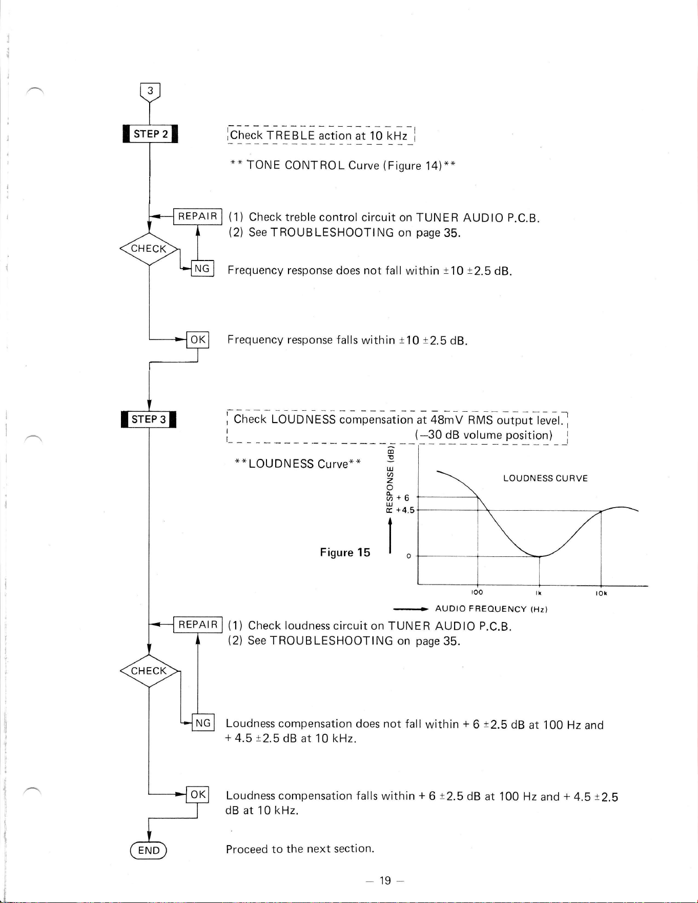
Check LOUDNESS
compensation
at 48mV
R-MS;tp;tl.r"r]
*"LOUDNESS
Curve"*
Figure
15
roo
tr
+
AUDIO FBEQUENCy
(Hz)
(1)
Check loudness
circuit on
TUNER
AUDIO
P.C.B.
(2)
See TROUBLESHOOTING
on
page
35.
Loudness
compensation
does not
fall
within
+
6
t2.5
dB
at 100 Hz
and
+
4.5
t2.5
dB at
10
kHz.
Loudness
compensation falls
within
+
6
!2.5
dB at
100 Hz
and
+
4.5
t2.5
dB at
10
kHz.
Proceed
to
the next section.
ll)
g
r..u
t,
z
o
e^
a+b
UJ
cc
+4.5
l.
(-30
dB volume
position)
i
-19-
REPAIR
CHECK
REPAIR
14
12
10
8
6
4
2
dB0
-4
-6
-8
_10
-12
-t4
i
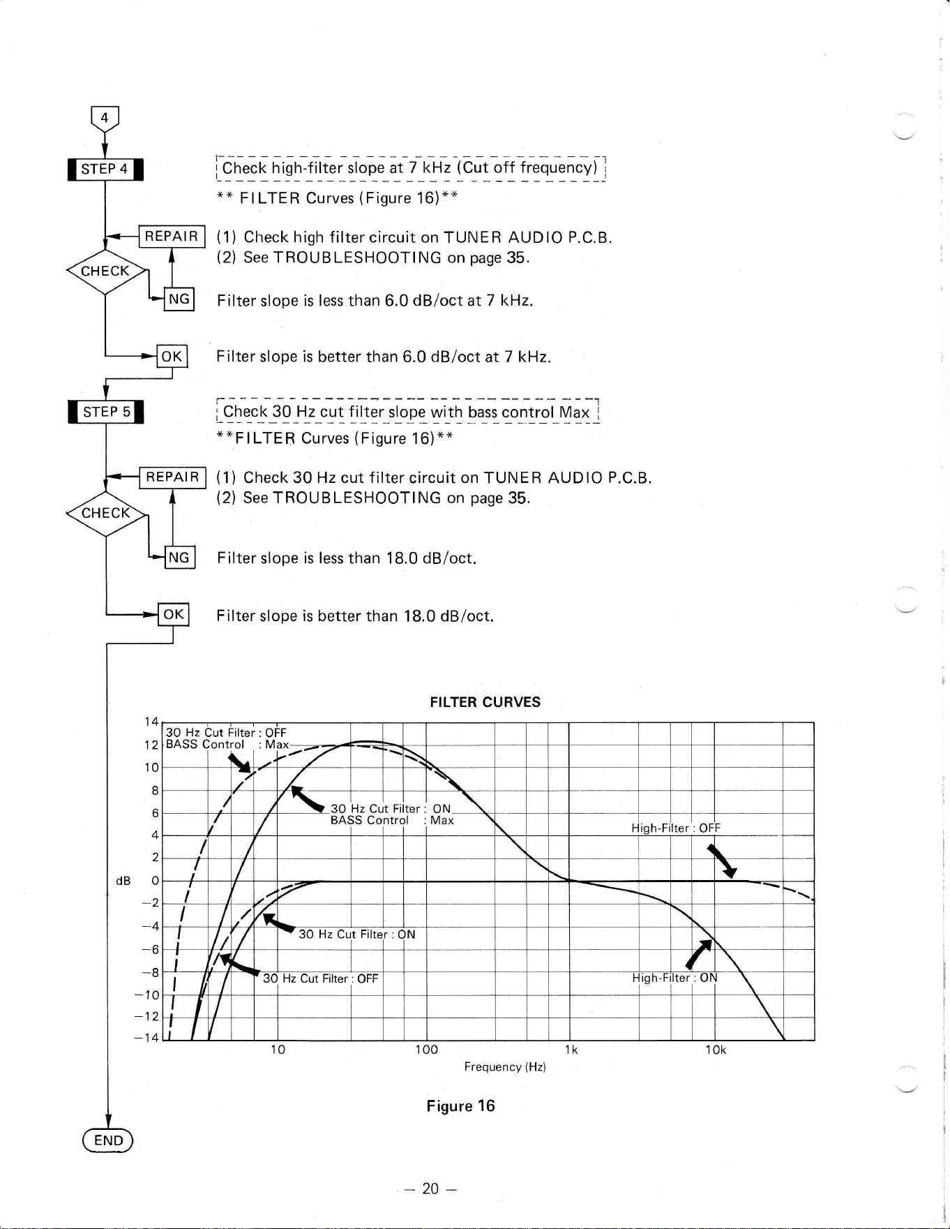
Ch."k
n-igl-'-ti
lGislop. rflt
n,
tcrt
oirlieqff"yil
**
FILTER Curves
(Figure
16)""
(1)
Check
high
filter circuit
on TUNER AUDIO
P.C.B.
(2)
See TROUBLESHOOTING on
page
35.
Filter
slope
is less than
6.0
dB/oct at7
kHz.
Filter
slope is
better than 6.0 dB/oct at 7 kHz.
;_C_ne_cl<_3Q_tlz_cy1!i!t9r_slorqy,_t!!ryr_qollrgt_Uil
j
"*FILTER
Curves
(Figure
16)**
(1)
Check 30
Hz
cut
filter
circuit
on
TUNER AUDIO
P.C.B.
(2)
See TROUBLESHOOTING on
page
35.
Filter
slope
is less
than 18.0 dB/oct.
Filter
slope
is better
than
18.0
dB/oct.
FILTER
CURVES
100
Frequency
(Hz)
Figure
16
30 Hz ut Filter :
OFF
\
'i:=--
\
,( \
\.o
I
Hz
Cut
Fi
o*\
BA{ iS Contrr
l
Max
H
qh-F
Iter
I
OFF
I
I
, /
I
--
I
I
'T
lt
/
3OHzC Filter :
I
)N
lt
I
JU riz
uut
Frlter
I
UFF
I
I
10
-20-
1k 10k
CONNECTION
REPAIR
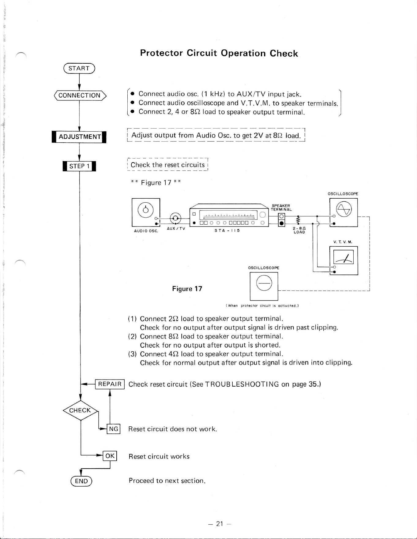
Protector
Circuit Operation
Check
Connect audio
osc.
(i
kHz)
to AUX/TV input
jack.
Connect audio
oscilloscope
and V.T.V.M. to
speaker terminals.
Connect
2,
4 or
8f)
load to
speaker
output
terminal.
f--
I
Adiust
output
from
Audio
Osc. to
get
2V at 8A load.
I
r--*- ------l
i
9
E:
!
tq
!.1"! 9,
l"yi!'_i
**
Figure 17
**
OSC ILLOSCOPE
AUDIO OSC.
Figure
17
(
Wh6n
pro'leclor
circuit
is oclivot€d.)
Connect
2O load
to
speaker
output
terminal.
Check
for no output after
output
signal
is
driven
past
clipping.
Connect
8Sl load
to
speaker
output terminal.
Check
for
no output
after
output
is
shorted.
Connect
4S/ load
to
speaker
output
terminal.
Check
for normal
output
after output signal
is
driven
into
clipping.
Check
reset circuit
(See
TROUB
LESHOOTING on
page
35.)
Reset
circuit does not
work.
Reset circuit works
Proceed
to
next
section.
(.
l.
l.
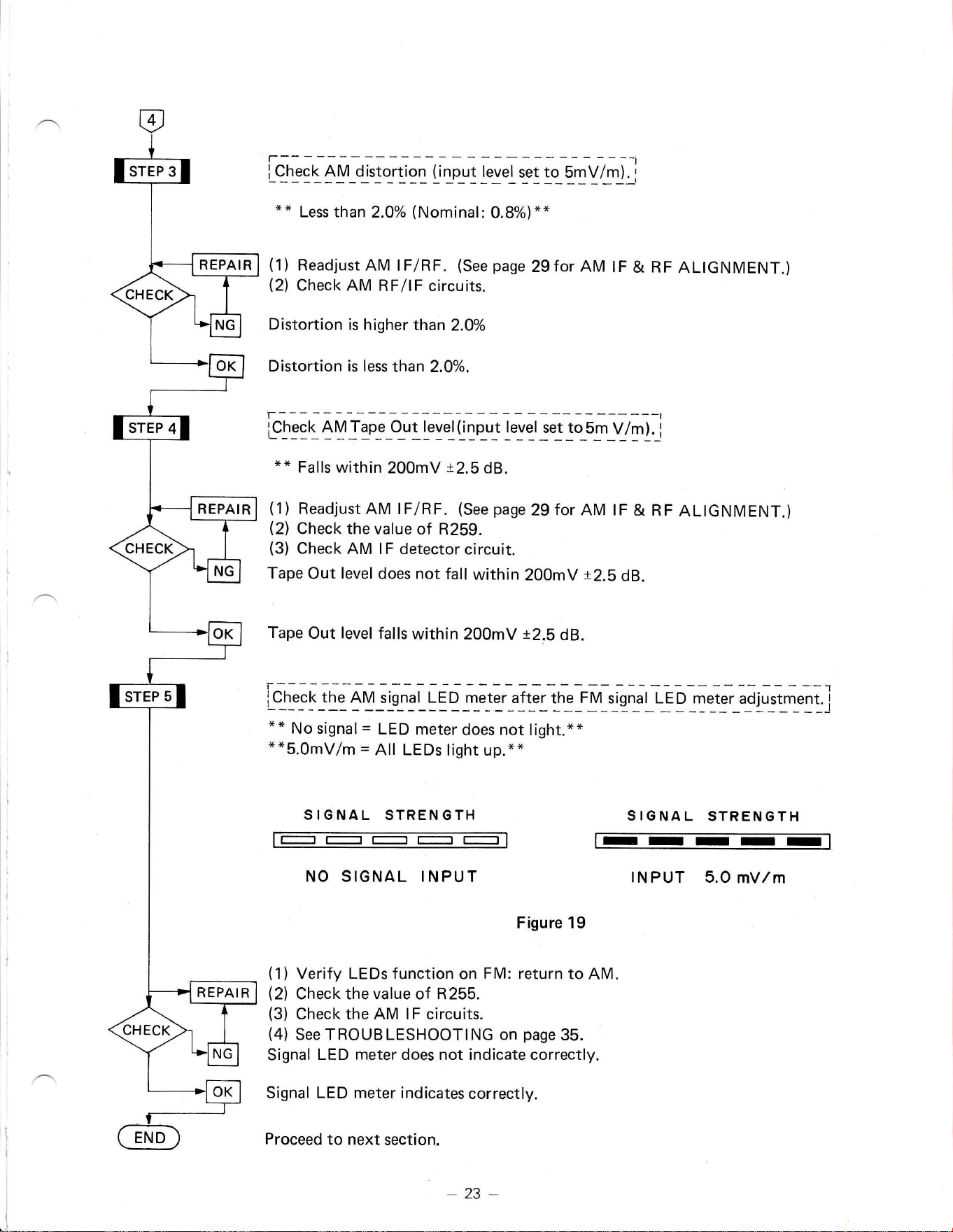
4
t
0
t
li
(
I
i
I
T
I
J
;t r'\
f,
(1)
(21
(3)
trtroootrtrtrtrtro
21
-
ADJUSTMENT
CONNECTION
REPAIR
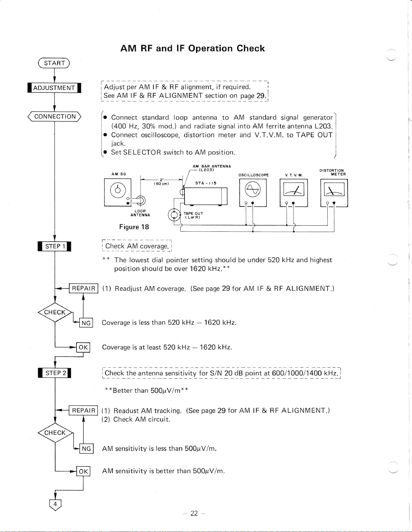
AM
RF and lF
Operation
Check
[na;"J;.r
AM G
&
RF
atisnment,
ir requ-t[0.-
--i
i_s_eg4y_t59
jI4_Llclyrli[_s3c_t1o1_ol_p_uq"_29_l
[.
Conn.", standard loop antenna to AM standard signal
generatorl
I
(400
Hz,
30%
mod.)
and radiate signal
into AM ferrite
antenna
L203.
I
i.
Connect osciiloscope, distortion
meter and V.T.V.M.
to TAPE
OUT;
I
jact.
I
[.
S". SE
LECTOR
switch to AM
position.
)
l_ 2'
lr$ I |
(6oc
L:i$
LOOP
ANTENNA
Figure
18
r---
-----t
l_9
tql!
3lL
c_9y
9
r9
s_e
: I
"*
The
lowest dial
pointer
setting should
be under 520
kHz
and highest
position
should
be over
1620
kHz.*"
(1)
Readjust AM coverage.
(See
page
29
for AM lF &
RF
ALIGNMENT.)
Coverage
is less than 520
kHz
-
1620 kHz.
Coverage is
at
least
52A
k1z
-
1620
kHz.
i_.lSg*!f
Sl;;J9,:r!r1,'_tv1"1_sl*_rga_q.f 1i_liooorlogqrrlootH,-.,
"*Better
than 500pV/m*"
(1)
Readust AM tracking.
(See
page
29
for AM lF & RF ALIGNMENT.)
(2)
Check AM
circuit.
AM sensitivity
is less
than
500pV/m.
AM
sensitivity
is better than 500pV/m.
-22
REPAI
R
REPAIR
------i
LQtf.gL
4ry1_{s1o_r191
llp_rl l.t.l t ! !o_!TY/j!_i
*+
Less than2.O%
(Nominal:
0.8%)**
(1)
ReadjustAM
lFlRF.
(Seepage
29Ior AM lF
&
RF
ALIGNMENT.)
(2)
Check
AM RF/lF circuits.
Distortion
is higher
than
2.Oo/o
Distortion is
less
than 2.0%.
f ---
- --------r
LcI'_.gL4YJ1pJ_o_r!!-ey.l!lqltleye_t3e_t1o_sf
_v/11._l
*"
Falls
within
200mV
t2.5
dB.
(1)
Readjust
AM lFlRF.
(See
page
29for
AM lF
& RF
ALIGNMENT.)
(2)
Check the value
of
R259.
(3)
Check
AM lF detector
circuit.
Tape
Out
level
does not
fall
within
200mV
t2.S
dB.
Tape
Out
level falls
within 200mV
t2.5
dB.
L.I"9I,
19
I
y_;gg'
i
io
rn.
t"
=It.'
tn1
1 rvrl
G
r. r
rE
b
...,:'_l.Lr:y.l
l]
;;
*; ;;,
r;;;;;;;;;;;;
;'*l;
**5.0mV/m
=
All LEDs
light up.*"
SIGNAL STRENGTH
NO SIGNAL INPUT
SIGNAL
STRENGTH
INPUT 5.O
mV/m
Figure 19
(1)
Verify
LEDs
function on
FM: return
to
AM.
(2)
Check the value of R255.
(3)
Check the AM lF circuits.
(4)
See TROUB LESHOOTING on
page
35.
Signal
LED
meter
does not indicate correctly.
Signal
LED meter
indicates
correctly.
Proceed
to next
section.
23
CONNECTION
REPAIR
REPAIR
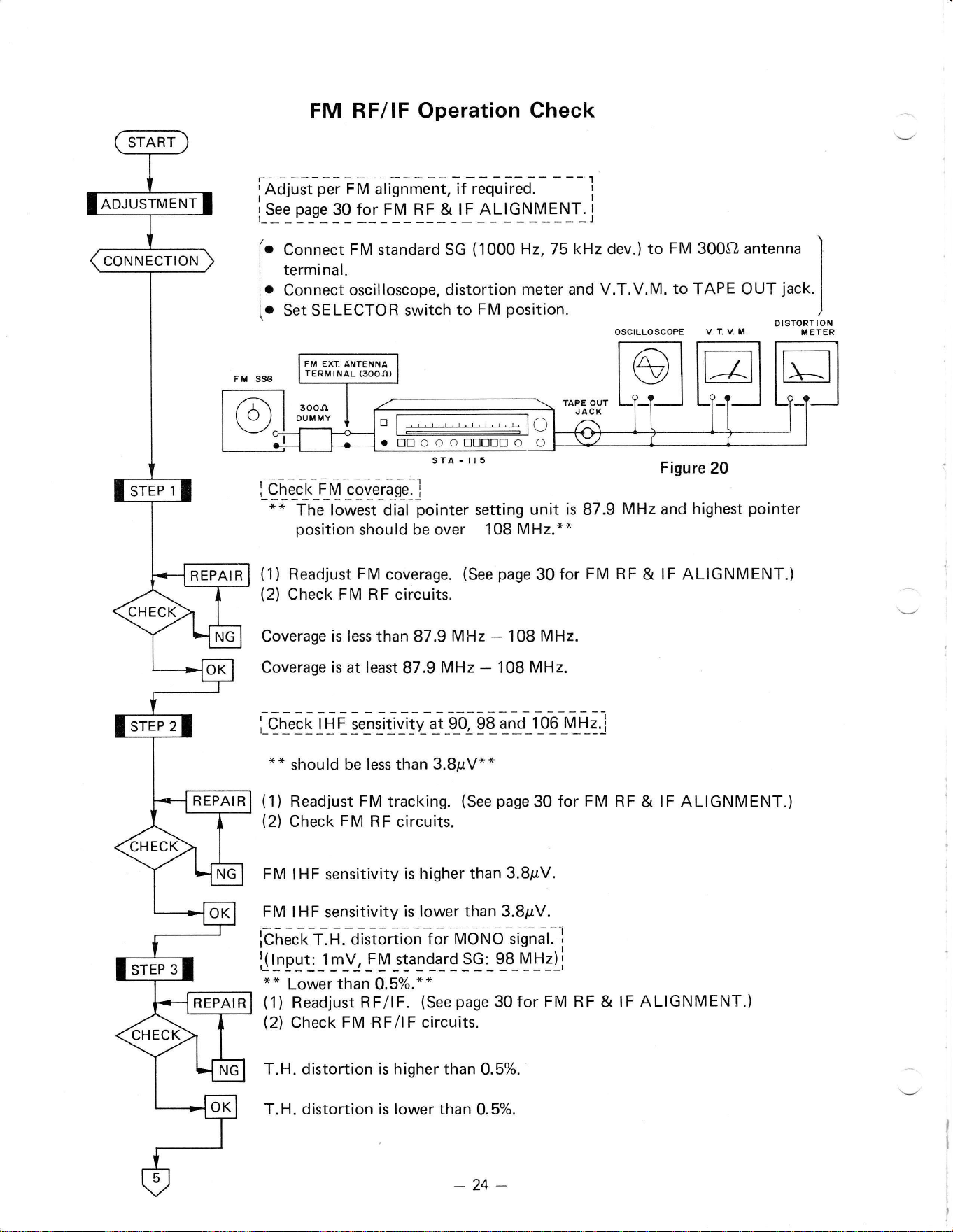
FM RF/lF Operation
Check
iAoirit
o*Frvr
,r[r*.ni,
if required.
I
i_t::
qrr:
99 l"rl[
II _q
[
4,1LGI[EIr.
i
f.
Conn""t
FM
standard SG
(1000
Hz, 75k{zdev.)
to
FM
3OOO antenna
)
I *rr"ri. I
l.
aonn.., oscilloscope,
distortion
meter
and
V.T.V.M.
to
TAPE OUT
Jack.
I
l.
S.t SELECTOR
switch
to
FM
position.
,,.ro"r,ln
V T. V. II.
METER
Figure 20
Lq 1a"l._iry s ei"rrs_"J
**
The lowest
dial
pointer
setting
unit
is
87.9
MHz
and
highest
pointer
position
should
be over 108
MHz."*
(1)
Readjust
FM
coverage.
(See
page
30for
FM
RF
&
lF ALIGNMENT.)
(2)
Check FM RF circuits.
Coverage
is less
than
87.9
MHz
-
108
MHz.
Coverage
is
at least
87.9
MHz
-
108
MHz.
[c-&s(Ili!.ll,r:yi,r-+-s-o.9Etlo-1.09]4Ii
j
"*
should
be
less
than
3.8trrV**
Readjust FM tracking.
(See
page
30
for FM RF
&
lF
ALIGNMENT.)
Check FM RF
circuits.
FM
IHF sensitivity
is
higher
than
3.8pV.
FM
IHF sensitivity
is lower than 3.8trrV.
iEr',"-"r.
t.
H. oirionio"lor
Molrro signJr.l
ll
l_ney U r_v_, I
y
_r1,!
qT9
_s 9,_
s_a_
Y Ir f
Ll
**
Lower
than
0.5%.*"
(1)
Readjust
RF/lF.
(See
pase
30 for
FM
RF
&
lF ALIGNMENT.)
(2)
Check
FM RF/lF circuits.
T.H.
distortion is higher
than 0.5%.
T.H. distortion is lower than
0.5%.
(1)
QI
\-/
I
trtroootrtrtrtrEo O
-24-
REPAI R
r----
------i
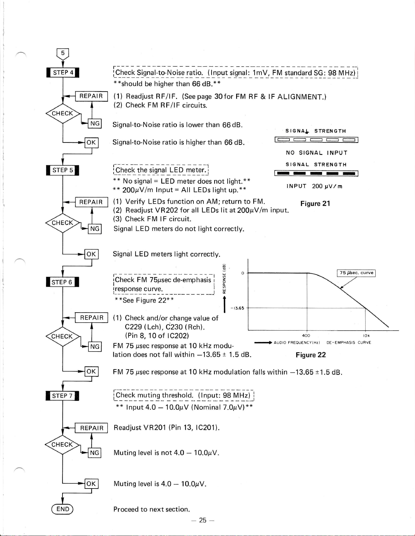
,c_[e_c\_s!01111t9-ltl_ois91ltto:
_(lpgt_srg1{._!1v_,IY
lte$St{!9.99]tl[zll
"
*should
be
higher
than
66 dB.**
(1)
Readjust
RF/lF.
(See
page
30for FM RF
&
lF
ALIGNMENT.)
(2)
Check FM
RF/lF circuits.
i
I
l
l
I
:
Signal-to-Noise ratio is lower than
66dB.
Signal-to-Noise ratio is higher than
66
dB.
I----
--
-
- -
--'l
;Check
the
signal
LED meter.
i
;
N;;',s;;rl LED ;;i.;;;;,
not
risht.**
*+
200pV/m
lnput
=
All LEDs light
up.**
(1)
Verify LEDs
function
on AM;
return to
FM.
(2)
Readjust
VR202 for
all
LEDs lit at
200pV/m
input.
(3)
Check
FM lF circuit.
Signal
LED
meters
do not
light correctly.
Signal
LED meters light
correctly.
f-_t--.-:---
---.--.-l
;Check
FM
75psec de-emphasis
i
[9P9]-s99!1-e:
-------
--
--]
*
*See
Figure
22"
*
(1
)
Check and/or
change value
of
C229
(Lch),
C230
(Rch).
(Pin
8,
10 of 1C202)
s
rG
NAl,.
STRENGTH
:
IUUUI__IL-II
NO
SIGNAL INPUT
SIGNAL
STRENGTH
ffi
INPUT
20O
1tv
/
m
Figure
21
400 rok
-
AUOIO FREOUENCY(Hz)
DE-EMPHASIS
CURVE
@
z
9
E
I-,..,
FM
75
psec
response at 10
kHz
modu-
lation does not fall
within
-13.65
t
1.5
dB.
Figure 22
FM
75
psec
response at 10 kHz modulation
falls
within
-13.65
t'1.5
dB.
isl
g{t
r ll,e
J ryT
[.lo.
I'J
q
ri t1t-u
ti)-i
**
lnput
4.0
-
10.OpV
(Nominal
7.0pV)"*
Readjust VR201
(Pin
13, 1C201).
Muting level is not 4.0
-
10.0pV.
Muting level is 4.0
-
10.0pV.
Proceed
to
next
section.
-25-
ADJUSTMENT
CONNECTION
FM
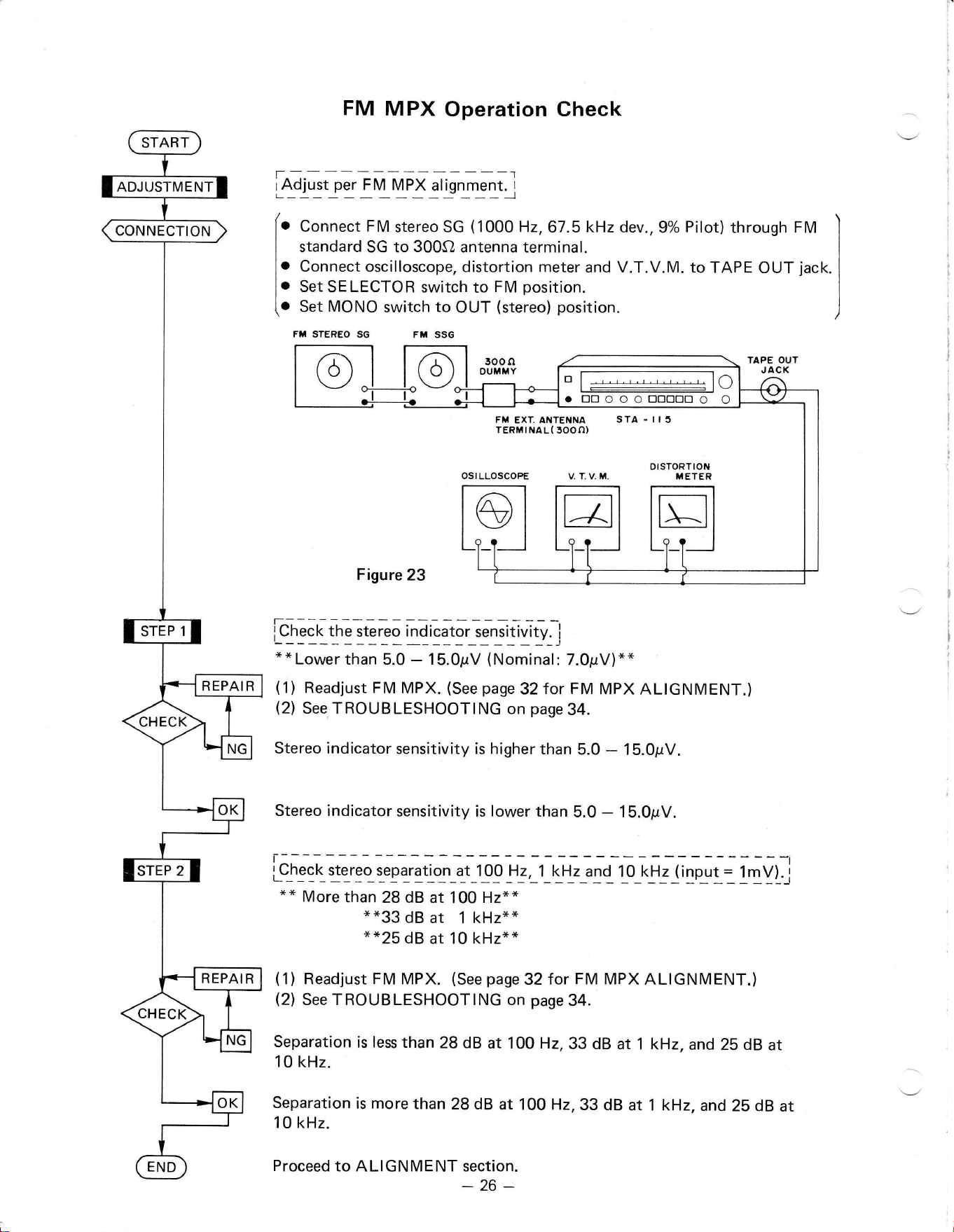
MPX
Operation Check
h;irGgtqU'li'itrry1{
(.
Conn...
FM
stereo SG
(1OOO
H2,67.5 kHz
dev.,
9%
Pilot)
through FM
l
I
standard SG to
3OOSI
antenna terminal.
I
l.
Conn""a oscilloscope,
distortion meter
and V.T.V.M.
to TAPE
OUT
jack.
I
l.
s.,
SELECTOR
switch to
FM
position.
I
l.
S.t
MONO
switch
to
OUT
(stereo)
position.
)
FT STEREO
SG FM
SSG
@
TAPE OUT
.,ACK
300n
DUIIMY
FM
EXT. ANTENNA
TERMINAL(
3OOO)
DISTORTION
tiETER
Figure
23
iq:it,Elt
Ei,le
!1,e l,e-f_-rl,
Lr.
i
;
;i";;
;;; 5n-- 1
S.opv
(
Nominat : 7.opV)
* *
(1)
Readjust
FM MPX.
(See
page
32for
FM
MPX
ALIGNMENT.)
(2)
See TROUBLESHOOTING
on
pase
34.
Stereo indicator
sensitivity is higher
than
5.0
-
15.0pV.
Stereo
indicator
sensitivity is
lower
than
5.0
-
15.0pV.
r:.--:
----r
lclgg[r]"_'go_1eg11t!o1_1t_L09ll,_t_Ll?_rlt'!_o_tf
t_zli1n_ut-:UyLi
**
More
than
28 dB
at 100
Hz*"
"*33
dB
at
1
kHz**
**25
dB
at 10 kHz**
(1)
Readjust
FM
MPX.
(See
page
32 tor
FM MPX
ALTGNMENT.)
(2)
See TROUBLESHOOTING on page
34.
Separation
is
lessthan
28
dB
at
100 H2,33
dB
at 1 kHz,
and 25 dB
at
1
0
kHz.
Separation
is more
than
28 dB
at 100 Hz,
33
dB at 1 kHz,
and 2b dB
at
1
0
kHz.
Proceed
to
ALTGNMENT
section.
_26_
Dnoootrtrtrotro
o
ALIGNM ENT I
NSTRUCTIONS
FM Coil
&
Trimmer Location
(Tuner,
Audio P.C.B.)
=
TR5O2
___-_J--t
t---L,l
I
I
'-^Ll
I
____r-l
--|
I
rl
lnl
lPl Rsrs
q/
#R
hru/
LtJ----:'/
.r
VR5OI for
AUST mod.lg
n
Rszo
lulffi
l(tsl
I I IVR5O2 lor
hJ
AUST modars
=
TR5OI
t-t
I
,_-,
7 t
D
E
---)
rrffi
It
ffi
H=
I
4
lt
I c--r t)
tt
trll
I
rzoz
rzot )rcaor I |
'----r
:-
ffiD
@@
Hld
tr
*--l
*r-Y
'r-t'
I l
J= [,*
@fqgryry
T
I r_
rr
"ib
-
uL_x_
I
i-
ere
rer:
I
r2.5
NNs+*Hffips
t->
I
N'fl-#'i6ii.#fu
iJ
_fl
,f,:_E
-ffi[J
-^t-l
qLr-
I--J
=rX/
t,:
UL
Figure
24
Note:
Refer
to
P.C.B.
illustration
for
alignment and adjustment
points.
-27
-
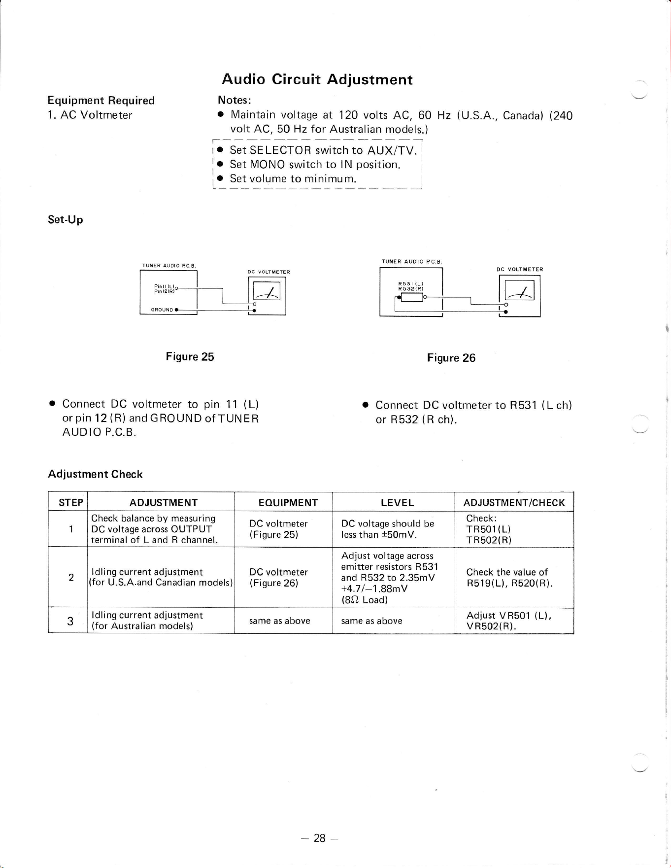
Equipment
Required
1. AC Voltmeter
Set-Up
Figure
25
.
Connect DC
voltmeter to
pin
1 1
(L)
orpin
12
(R)
andGROUND
of
TUNER
AUDIO P.C.B.
Adjustment
Check
Audio
Circuit Adjustment
Notes:
o
Maintain
voltage
a'r. 12O volts
AC, 60 Hz
(U.S.A.,
Canada)
(240
volt
AC,
50
Hz for
Australian models.)
I.-s",;E
L
-r
o; *I..
r,,.-n
u
vrI
l.
S., MONO
switch
to lN
position.
i
Lil.lfgrylolrry, ____
|
TUilER
AUOIO PC.B.
DC VOLTMETER
lffi
r,--Il
Figure
26
o
Connect
DC voltmeter to
R531
(L
ch)
or
R532
(R
ch).
STEP
ADJUSTMENT
EOUIPMENT
LEVEL
ADJUSTMENT/CHECK
1
Check balance by measuring
DC voltage across OUTPUT
terminal of L and
R
channel.
DC voltmeter
(Figure
25)
DC voltage
should
be
less
than
t50mV.
Check:
TR501(L)
TR502(R)
2
I dli ng
current adjustment
for
U.S.A.and Canadian models
DC voltmeter
(Figure
26)
Adjust
voltage
across
emitter
resistors R531
and
R532
to 2.35mV
+4.71-1.88mV
(8O
Load)
Check the value of
R519(L), R520(R).
3
ldling
current adjustment
(for
Australian models)
same as above
same as above
Adjust
VR501
(L),
vR502(R).
-28-
Equipment
Required
1.
AM standard
signal
generator
2. Standard
loop
antenna
3.
Oscilloscope
4.
AC voltmeter
5.
Distortion
meter
Set-Up
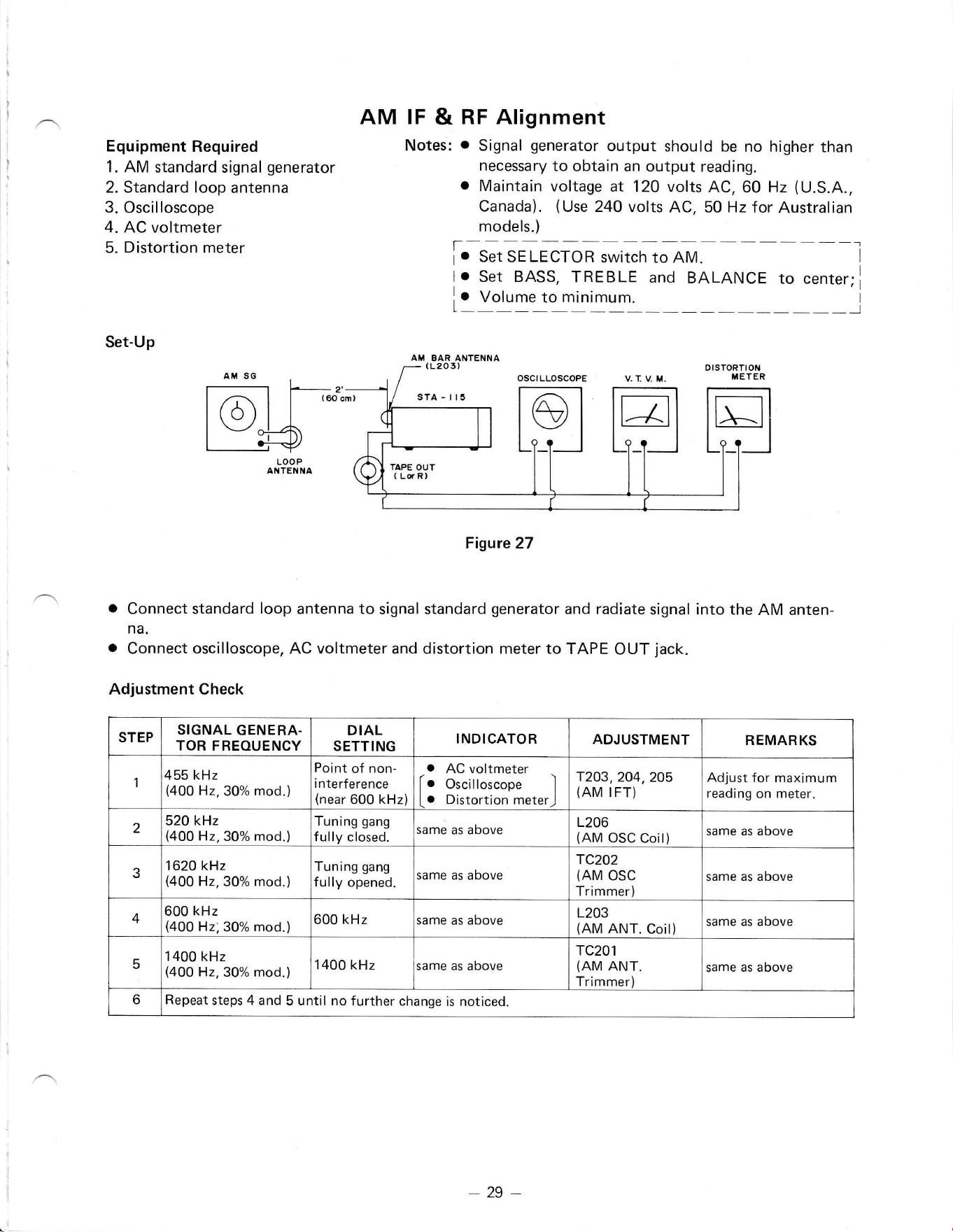
Connect standard
loop
antenna to
signal
na.
Connect
oscilloscope,
AC
voltmeter
and
Adjustment Check
AM lF
&
RF Alignment
Notes:
o
Signal
generator
output
should
be no higher
than
necessary
to
obtain an
output reading.
o
Maintain voltage
at 12O volts
AC, 60
Hz
(U,S.A.,
Canada).
(Use
240 volts
AC, 50 Hz
for
Australian
models.)
f-
lo
Set
SELECTOR
switch to AM.
I
o
Set BASS,
TREBLE
and
BALANCE
to
""nt"r;l
1Y"r,t"l11rrr,
_____l
Figure 27
standard
generator
and radiate
signal
distortion meter to
TAPE
OUT
jack.
into the
AM anten-
TAPE
OUT
(
LdR)
STEP
SIGNAL
GENERA-
TOR
FREOUENCY
DIAL
SETTING
INDICATOR
ADJUSTMENT
REMARKS
455 kHz
(400
H2,30%
mod.)
Point
of
non-
i nterference
(near
600 kHz)
a
AC voltmeter
Io
oscilloscope
I
I
o
Distortion
.et.rJ
T203,204,205
(AM
IFT)
Adjust for maximum
reading
on
meter.
2
52O kHz
(400
H2.30%
mod.)
Tuning
gang
f ully
closed.
;ame
as above
L206
(AM
OSC Coil)
same as above
3
1620 kHz
(4O0
H2,30% mod.)
Tuning
gang
fully opened.
;ame as above
rc202
(AM
OSC
Trimmer)
same as above
4
600 kHz
(400
Hz;30% mod.)
600
kHz
;ame
as above
L203
(AM
ANT.
Coil)
same as above
5
1
400
kHz
(400
H2,30%
mod.)
1400
kHz
;ame
as
above
TC2O1
(AM
ANT.
Trimmer)
same
as above
6 Repeat
steps 4 and
5 until no
further change
is noticed.
-29-
FM RF
&
lF
Alignment
Notes:
o
Signal
generator
output should be no higher
than
necessary
to obtain
an output reading.
o
Maintain voltage
at 12O volts
AC, 60 Hz
(U.S.A.,
Canada).
(Use
240 volts AC,
50
Hz for
Australian
models.)
ti-set
sEr-Edron
s*itcrr io-rvr.
--
--i
l-.-t_.t
MoNo
switch
to
oUT
(stereo)
position.
I
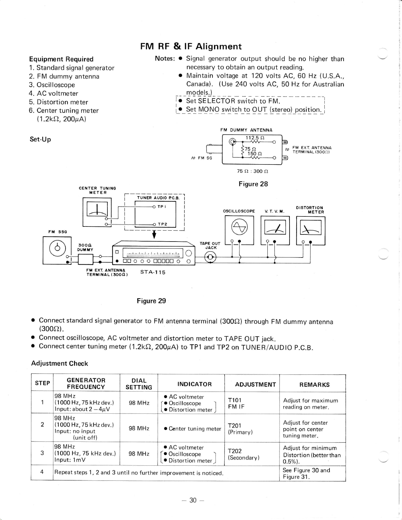
Equipment Required
1. Standard
signal
generator
2.
FM
dummy
antenna
3. Oscilloscope
4.
AC voltmeter
5. Distortion
meter
6. Center tuning meter
(1.2kSr,
200pA)
Set-Up
FM
EX'[
ANTENNA
TERMINAL
(3OOO)
/A FM
SG
CENTER
TUilING
r.ET
E R
75 rl
:3O0
rt
Figure
28
oscrLLoscoPE
orsroRTtoN
V,
T. V- M.
METER
iHi;,filllilie,
srA-115
Figure 29
Connect standard
signal
generator
to
FM antenna
terminal
(300Sl)
through
FM
dummy
antenna
(300s2).
connect
oscilloscope,
AC voltmeter
and
distortion meter
to
TApE
oUT
jack.
Connect
center
tuning meter
(1.2ksr,
200pA) to
TP1
andTp2
on
TUNER/AUDlo
p.C.B.
Adjustment
Check
a
a
FM
DUMMY
ANTENNA
trtroootrDODtro
STEP
GENERATOR
FREOUENCY
DIAL
SETTING
INDICATOR
ADJUSTMENT
REMARKS
98
MHz
(
1 000
Hz, 75
kHz
dev.)
lnput:
about
2
-41tV
98
MHz
o
AC
voltmeter
Io
Oscilloscope
I
lo
Distortion
meter
J
T1 01
FM
IF
Adjust
for
maximum
reading
on
meter.
2
98 MHz
(
1
000
H2,75 kHz
dev.)
lnput:
no input
(unit
off)
98 MHz
o
Center
tuning meter
T201
(Primary)
Adjust
for center
point
on
center
tuning meter.
3
98
MHz
(1000
Hz,
75 kHz
dev.)
lnput:
1mV
98 MHz
o
AC
voltmeter
[o
Oscilloscope
'l
Io
Distortion
meterJ
T202
(Secondary)
Adjust for minimum
Distortion
(
better than
0.5%).
4 Repeat
steps
1,
2 and
3 until
no further
improvement
is noticed.
See
Figure
30 and
Figure
31.
-30-
STEP
GENERATOR
FREOUENCY
DIAL
SETTING
INDICATOR
ADJUSTMENT
REMARKS
5
87.9 MHz
(1000
H2,75
kHz
dev.)
lnput
1mV
87.9
MHz
.AC
voltmeter
[o
Oscilloscope
'l
[.
Dirtortion
meter-J
L 105
(FM
OSC.
Coil)
Adjust
for maximum
reading
on
meter.
6
108
MHz
(1000
H2,75 kHz
dev.)
108 MHz
.AC
voltmeter
[o
Oscilloscope
I
[o
Distortion
m"terJ
TCi
03
(FM
OSC.
Trimmer)
Adjust for maximum
reading
on meter.
1
Repeat
steps 5 and
6 unt
90 MHz
(1000
Hz,
75 kHz
dev.)
lnput:
about
2
-
41tY
no further
improvement
is
noticed.
I
|
'AC
voltmeter
90 MHz
| [.Oscilloscope I
|
[oDistortion
meter_J
1101
(FM
I
antennacoil) l
-.
Lf
OS iiM R'r I
Adjust for
maximum
*ii
-'r,i.,"r,
or I
reading
on
meter'
squeeze)
|
I
106
MHz
(1000
H2,75
kHz
dev.)
lnput:
about
2
-
4pY
106
MHz
o AC
voltmeter
l-o
Oscilloscope
I
Lo
Distorti
on mete
r-..]
TCi01
(FM
an-
tenna
trimmer)
TC1O2
(FM
RF
trimmer)
Adjust
for maximum
reading
on
meter.
10
Repeat
steps
8
and
9 unti no
further
improvement
is noticed.
11
98
MHz
(1000
Hz, 75 kHz
dev.)
lnput:
4
-
1OpV
98 MHz
oAC
voltmeter
[oOscilloscope I
[o
Distortion
meter_J
VR201
(Mute
threshold
adj.)
Set selector
to FM
mute
and
adiust
VR201
for
no
signal
output.
12
98
MHz
(1000
H2,75
kHz
dev.)
lnput:
200prV
98 MHz
oSignal
meter
(LEDs)
on
set.
VR2O2
(FM
signal meter
adj.
)
Adjust
until
all the
signal
LEDs
light.
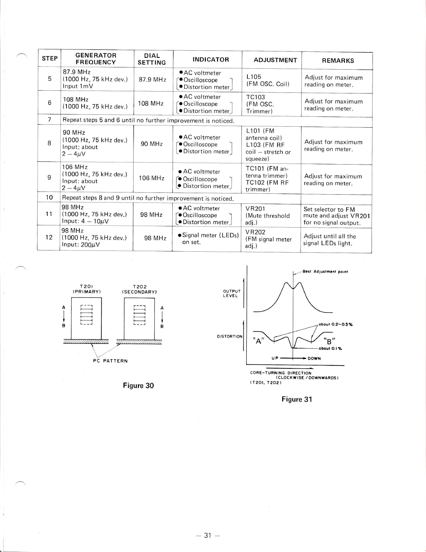
T
20t
(PRIMARY)
r?o2
(
SECONOARY)
Figure
30
OUTPUT
L EVEL
B?rl
Adjurtm.nt
poin,
oboul
O-2-O3*
\TB"
oboul O I
'16
H
o,rrorflo*l
"A"
PC PATTERN
DOWN
CORE-TURNING
OIRECTION
(cLocKwtsE
/ oowNwaRos
)
tT20t,1202t
Figure
31
tr--1
L_-J
-3'l
-
FM Stereo
(Multiplex
Equipment Required
1.
Stereo
modulator
Modulation level of
19
kHz
Pilotsignal
. . . . . 8
-
10%
2.
FM
signal
generator
Output
level
-
1mV
Frequency
-
Approximately 98
MHz
Deviation
-
75
kHz, 100% deviation
3.
Audio
generator
of composite
signal
4.
AC
voltmeter
5.
Oscilloscope
6. Distortion
meter
7.
Frequency counter
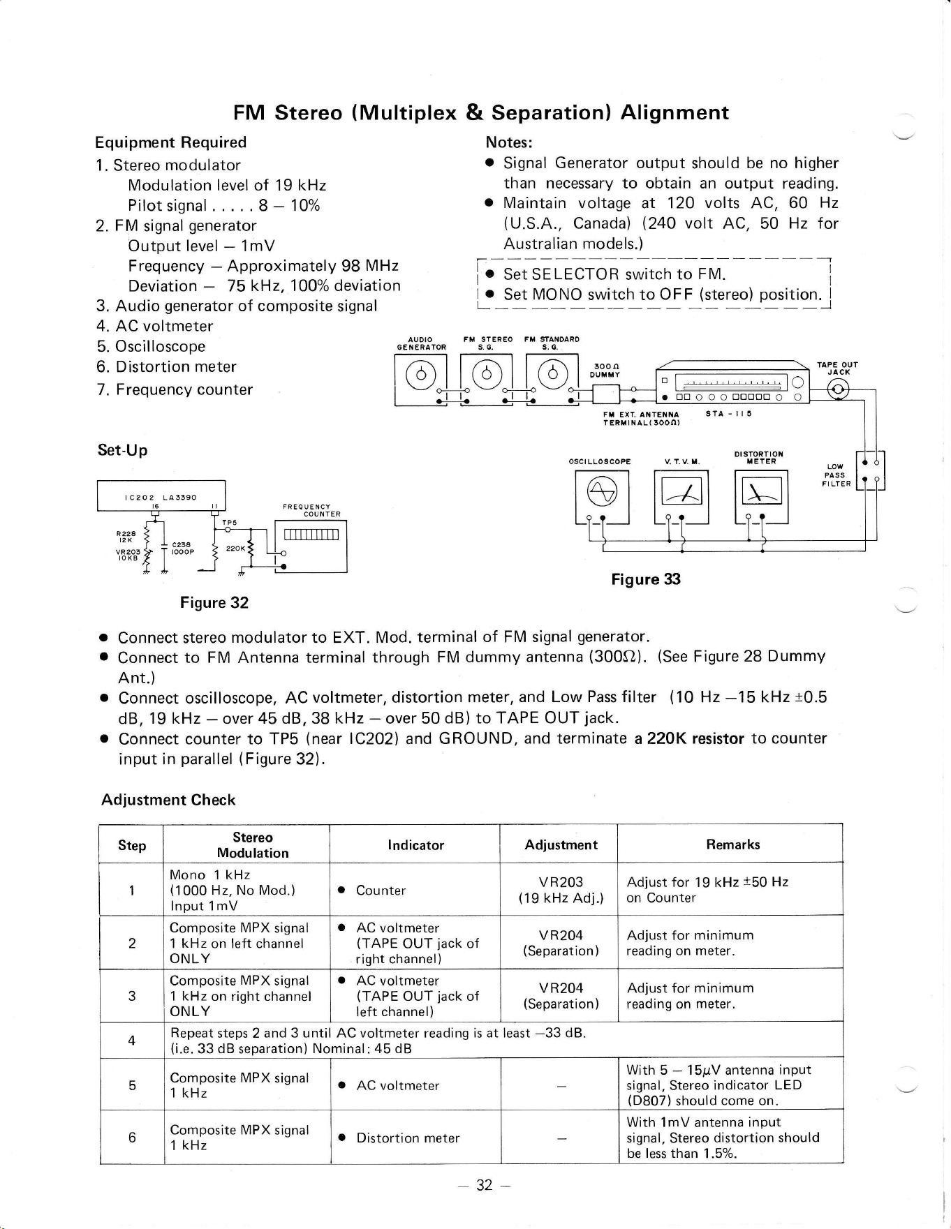
Set-Up
au 0ro
G ENERATOR
& Separation)
Alignment
Notes:
o
Signal
Generator output
should
be no higher
than necessary to obtain an
output reading.
.
Maintain voltage
at 120
volts
AC, 60
Hz
(U.S.A.,
Canada)
(240
volt
AC, 50
Hz for
Australian
models.)
i----
I
.
S.. SELECTOR switch
to
FM.
I
I
e
Set
MONO
switch to
OFF
(stereo)
position.
I
L___
--]
FM STEREO FM STANOARO
s. G. s.6.
a
a
Figure
33
Figure
32
Connect stereo
modulator
to EXT.
Mod. terminal
of
FM
signal
generator.
Connect
to FM
Antenna
terminal through
FM dummy
antenna
(300S}).
(See
Figure
28
Dummy
Ant.)
Connect oscilloscope,
AC
voltmeter, distortion
meter, and Low Pass filter
(10
Hz
-15
kHz
t0.5
dB,
19 kHz
-
over 45 dB, 38 kHz
-
over 50
dB) to TAPE OUT
jack.
Connect
counter to TP5
(near
lC2O2)
and
GROUND,
and
terminate a22OK
resistor to counter
input in
parallel
(Figure
32).
Adjustment
Check
TAPE OUT
JACK
FX
EXT. A(TEiliA
TERHINAL(3OON)
"f,.*'-,-',-,-
lO
.
tr0oOoDOtrtrOO
O
I C202 LA3390
Step
Stereo
Modulation
lndicator Adjustment
Remarks
1
Mono 1 kHz
(1000
Hz, No Mod.)
lnput 1mV
a
Counter
VR2O3
(19
kHz
Adj.)
Adjust
for 19 kHz
t50
Hz
on
Counter
2
Composite MPX
signal
1
kHz
on left channel
ONLY
.
AC voltmeter
(TAPE
OUT
jack
o{
right channel)
VR2O4
(Separation
)
Adjust for
minimum
reading
on meter.
3
Composite
MPX
signal
1
kHz
on right channel
ONLY
.
AC voltmeter
(TAPE
OUT
jack
of
left
channel)
V R2O4
(Separation
)
Adjust for
mlnimum
reading
on
meter.
4
Repeat
steps 2
and
3
until
AC
voltmeter
reading
is at least
-33
dB.
(i.e.
33 dB separation)
Nominal: 45 dB
5
Composite MPX signal
1 kHz
.
AC
voltmeter
With
5
-
15ptV antenna
input
signal, Stereo
indicator
LED
(D807)
should
come on.
6
Composite MPX
slgnal
1
kHz
a
Distortion meter
With
1mV
antenna
input
signal, Stereo
distortion should
be less than
1.5%.
32-
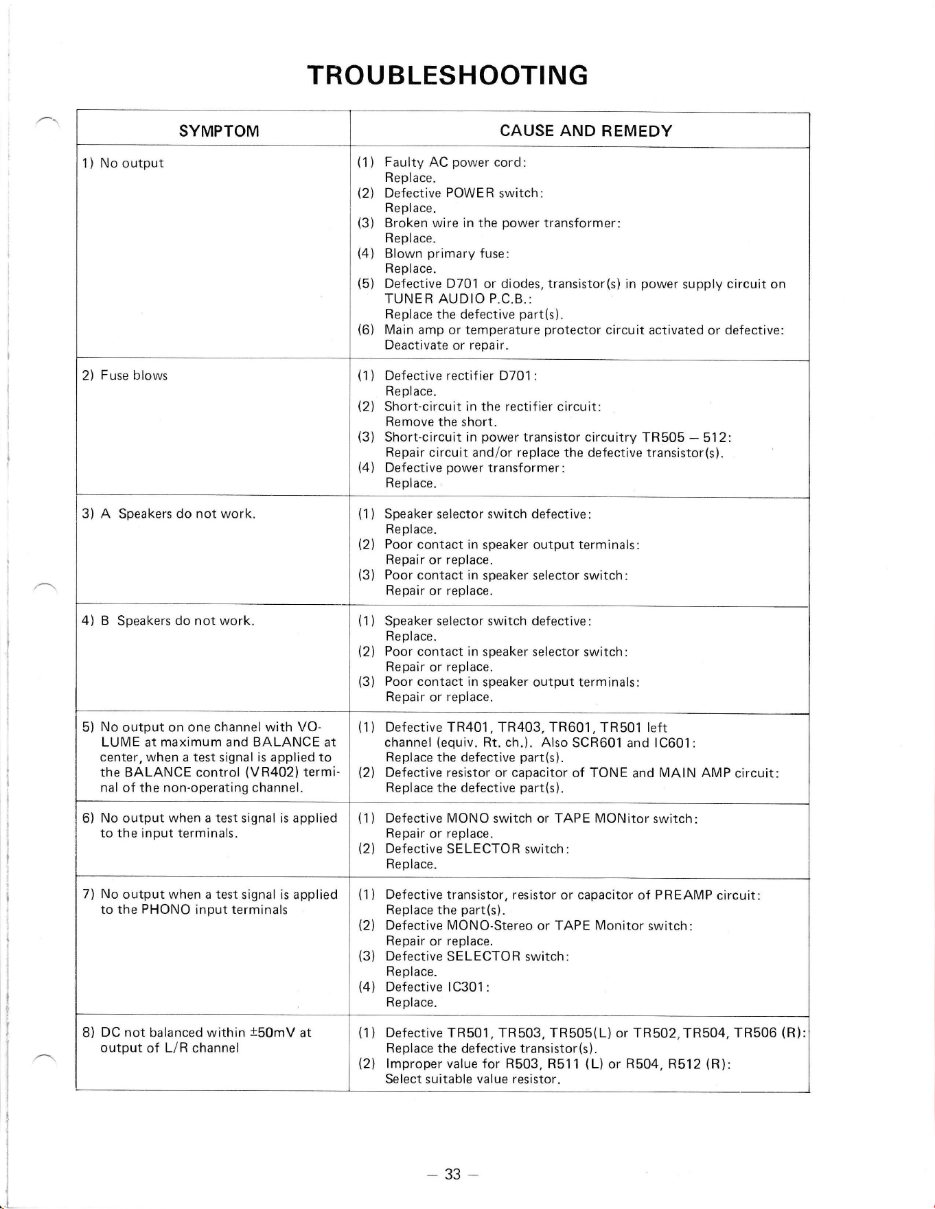
SYMPTOM
CAUSE AND REMEDY
1
)
No output
Faulty AC
power
cord:
Replace.
Defective
POWE
R
switch
:
Re
pl
ace.
Broken wire in the
power
transformer:
Replace.
Blown
primary
fuse:
Replace.
Defective D701
or diodes,
translstor(s)
in
power
supply
circuit
on
TUNER AUDIO P.C.B.:
Replace
the
defective
part(s).
Main amp
or
temperature
protector
circuit
activated
or
defective:
Deactivate
or
repair.
(1)
12\
(3)
(4)
(5)
(6)
2)
Fuse
blows
(1
)
Defective rectif ier D701 :
Replace.
(2)
Short-circuit in the rectifier circuit:
Remove
the short.
(3)
Short-circuit
in
power
transistor
circuitry TR505
-
512'.
Repair
circuit and/or replace the defective transistor(s).
(4)
Defective
power
transformer:
Replace.
3) A Speakers
do not work.
Speaker selector
switch defective
:
Replace.
Poor
contact in
speaker
output terminals:
Repair
or replace.
Poor
contact in
speaker selector switch:
Repair
or replace.
(1)
(2\
(3)
4) B
Speakers
do
not
work.
(1)
Speaker selector
switch defective:
Replace.
(2)
Poor
contact in speaker selector
switch:
Repair
or
replace"
(3)
Poor
contact in
speaker output terminals
Repair or
replace.
5)
No
output
on one channel with VO-
LUME at maximum and BALANCE at
center, when
a
test
signal
is applled to
the BALANCE control
(VR402)
termi-
nal
of
the non-operating channel.
(1)
Defective
TR401, TR403,
TR601.
TR501 left
channel
(equiv.
Rt.
ch.).
Also
SCR601 and 1C601
:
Replace
the defective
part(s).
(2)
Defective resistor
or
capacitor
of TONE
and
MAIN AMP
circuit
Replace
the
defective
part(s).
6)
No output when a test signal
is
applied
to the
input
terminals.
(1
)
Defective MONO
switch or TAPE MONitor
switch:
Repair
or
replace.
(2)
Defective
SELECTOR switch:
Replace.
7)
No
output when
a
test
signal is applied
to the
PHONO
input
terminals
(1
)
Defective
transistor,
resistor or capacitor
of
PREAMP
circuit:
Replace the
part(s).
(2)
Defective MONO-Stereo
or TAPE
Monitor
switch:
Repair
or
replace.
(3)
Defective
SELECTOR
switch:
Replace.
(4)
Defective
1C301 :
Replace.
8)
DC not
balanced within
l50mV
at
output
of
L/R
channel
(i
)
Defective
TR501, TR503, TR505(L) or TR502,TR504, TR506
(R)
Replace
the defective transistor(s).
(2)
lmproper
value for R503, R511
(L)
or
R504.
R512
(R):
Select suitable
value
resistor.
TROU BLESHOOTING
-33-
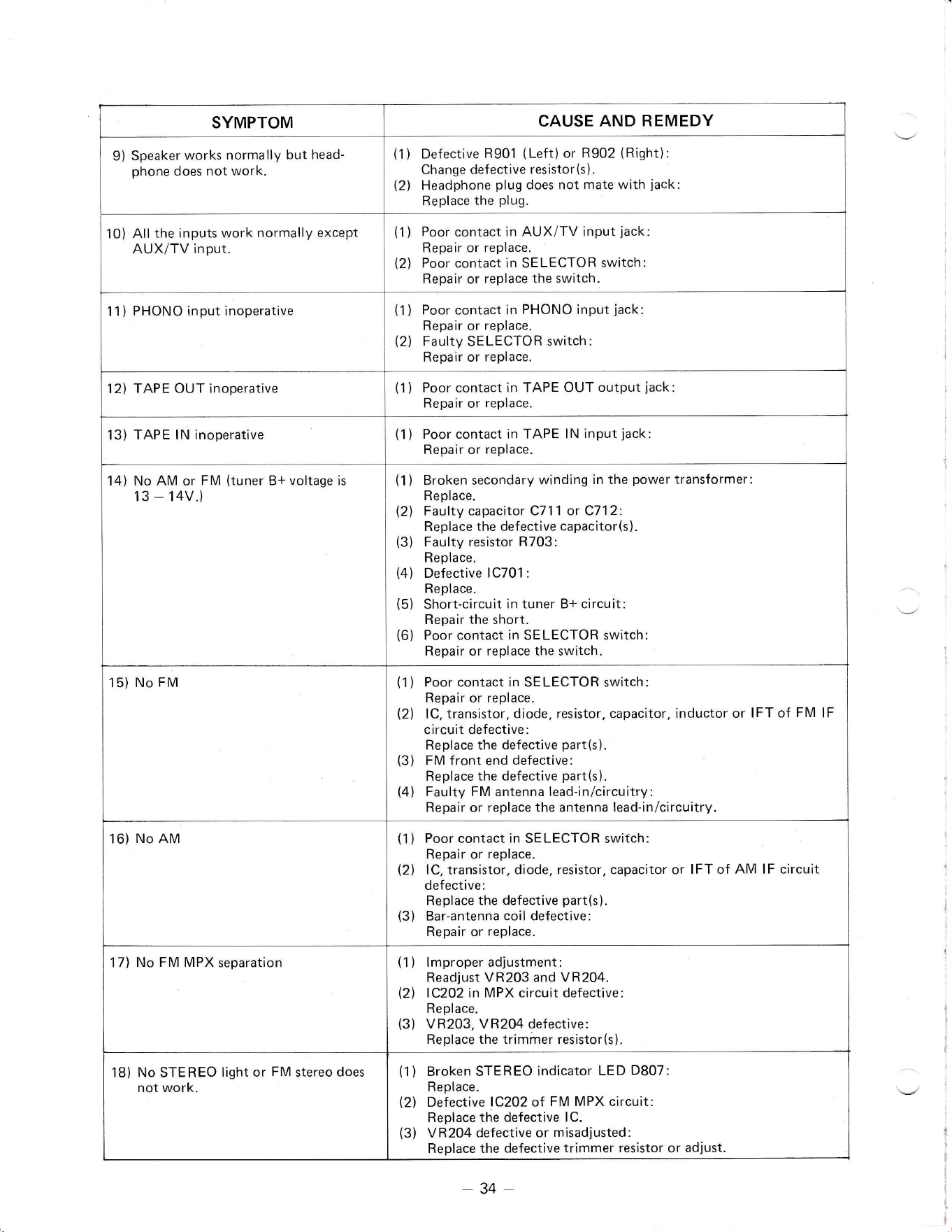
SYMPTOM
CAUSE AND
REMEDY
9) Speaker
works
normally
but head-
phone
does not
work.
(1
)
Defective
R901
(Left)
or
R902
(Right):
Change
defective
resistor(s).
(2)
Headphone
plug
does not
mate with
jack:
Replace
the
plug.
10)
All the
inputs work
normally except
AUX/TV
input.
(1)
Poor
contact
in AUX/TV input
jack:
Repair
or replace.
(2)
Poor contact in SELECTOR
switch:
Repair
or
replace the
switch.
11)
PHONO input inoperative
(1)
Poor contact in
PHONO input
jack:
Repair or
replace.
(2)
Faulty SELECTOR
switch:
Repair or
replace.
12)
TAPE
OUT
inoperative
(1
)
Poor
contact
In TAPE OUT
output
jack:
Repair
or
replace.
13)
TAPE lN inoperative
(1)
Poor contact in TAPE lN
input
jack:
Repair or replace.
14) No
AM
or
FM
(tuner
B+
voltage
is
13
-
14V.)
(1)
Broken secondary
winding
in the
power
transformer:
Replace.
(2)
Faulty
capacitor
C711 or C712:
Replace the defective
capacitor(s
).
(3)
Faulty resistor
R703:
Replace.
(4)
Defective
1C701:
Replace.
(5)
Short-circuit
in tuner B+ circuit:
Repair the short.
(6)
Poor contact in SELECTOR switch:
Repair
or
replace the switch.
15)
No
FM
(1)
Poor contact in SELECTOR switch:
Repair or replace.
(21
lC,
transistor, diode, resistor, capacitor.
inductor or
IFT of
FM
lF
circuit defective:
Replace the defective
part(s).
(3)
FM front end
defective:
Replace the defective
part(s).
(4)
Faulty FM antenna lead-in/circuitry:
Repair
or
replace the antenna
lead-in/circuitry.
16)
No AM
(1)
Poor
contact
in
SELECTOR switch:
Repair or
replace.
(2)
lC,
transistor,
diode, resistor, capacitor or
IFT of AM lF circuit
defective:
Replace the defective
part(s).
(3)
Bar-antenna
coil defective:
Repair
or
replace.
17) No
FM MPX
separation
(1
)
lmproper adjustment:
Readjust VR203 and
VR204.
(2\
lC2O2 in MPX
circuit
defective
Replace.
(3)
VR203, VR204 defective:
Replace
the trimmer resistor(s)
18)
No
STEREO
light
or
FM
stereo
does
not work.
(1)
Broken STEREO
indicator
LED
D807:
Replace.
(2)
Defective
lC2O2
of
FM MPX circuit:
Replace
the defective
lC.
(3)
VR204 defective
or
misadjusted;
Replace the defective
trimmer resistor
or
adjust
-34
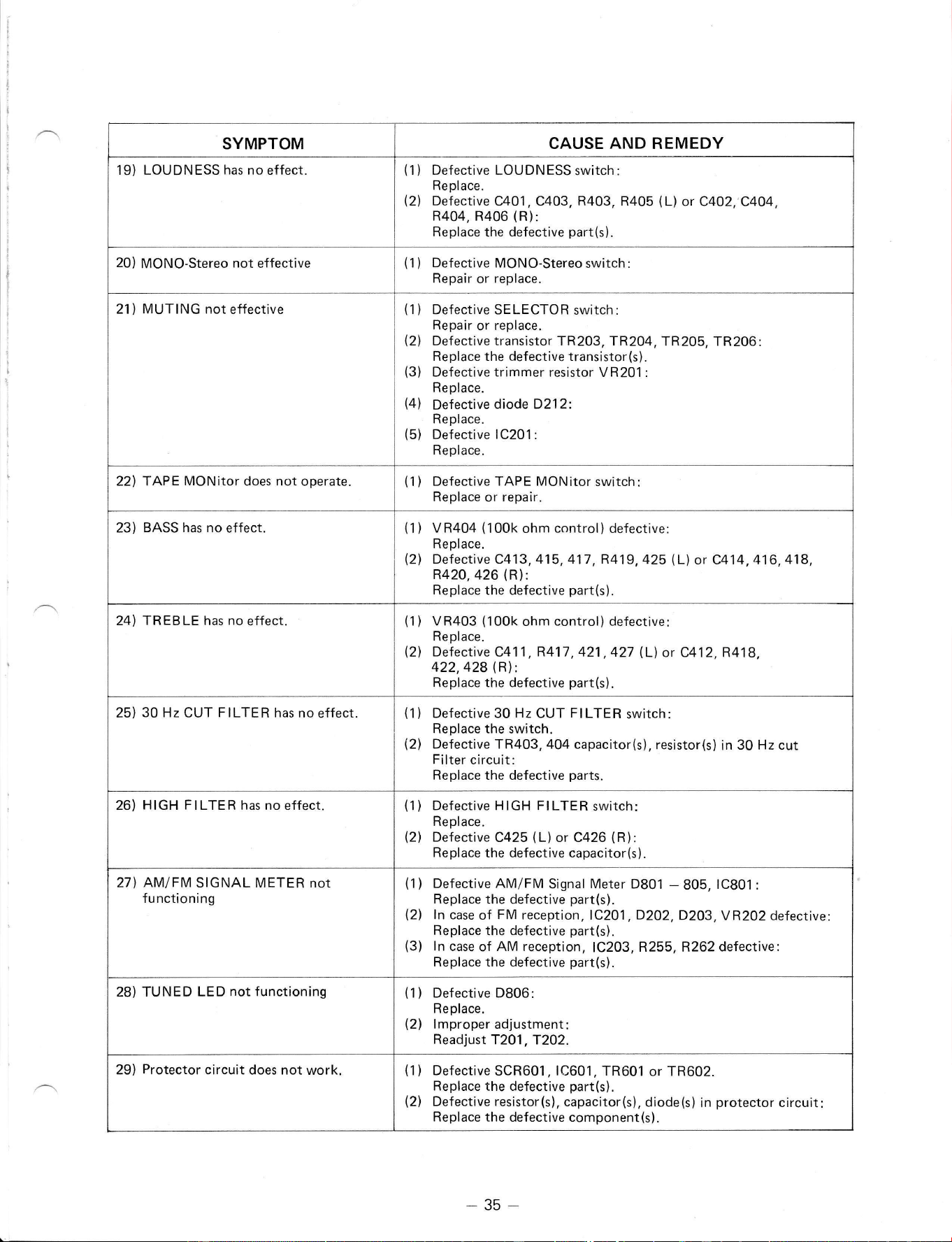
SYMPTOM CAUSE AND REMEDY
19) LOUDNESS
has no
effect.
(1)
Defective LOUDNESS
switch:
Replace.
(2)
Defective C401, C403, 8403, R405
(Ll
or C4A2,C4O4,
R404,
R406
(R):
Replace
the
defective
part(s).
20)
MONO-Stereo
not
effective
(1
)
Defective
MONO-Stereo
switch :
Repair
or
replace.
21)
MUTING not
effective
('l
)
Defective SELECTOR
switch:
Repair
or
replace.
(2)
Defective transistor TR203, fR2O4,
TR205, TR206:
Replace the defective transistor(s).
(3)
Defective trimmer resistor
VR201 :
Replace.
(4)
Defective
diode D21 2:
Replace.
(5)
Defective
1C201
:
Replace.
22l' T
APE MONitor
does not operate.
(1
)
Defective TAPE
MONitor
switch:
Replace
or
repair.
23)
BASS has
no effect.
(1)
(21
VR404
(100k
ohm control) defective:
Replace.
Defective
C413,
415, 417, R419,
425
(Ll
or C414, 416,
418,
R420,426
(Rl:
Replace the defective
part(s).
24) TREBLE has
no
effect.
(1)
VR403
(100k
ohm control) defective:
Replace.
(2)
Defective
C411
,
R417
,421 ,427
(tl
or C412, R418,
422,428
(Rl:
Replace the defective
part(s).
25)
30 Hz
CUT
FILTER
has no
effect.
(1)
Defective 30 Hz CUT
FILTER
switch:
Replace the
switch.
(2)
Defective TR403,
404 capacitor(s),
resistor(s)
in
30 Hz
cut
Filter
circuit:
Replace the defective
parts.
26)
HIGH FILTER
has no effect.
(1)
Defective HIGH FILTER
switch:
Replace.
(2)
Defective
C425
(Ll
or C426
(R):
Replace
the defective capacitor(s).
271
AMIFM
SIGNAL METER not
functioning
(1)
Defective AM/FM
Signal Meter D801
-
805,
1C801:
Replace
the defective
part(s).
(2)
ln case
of
FM
reception, 1C201
,
D2O2,
D2O3,VR2O2
defective:
Replace
the
defective
part(s).
(3)
ln
case
of
AM reception,
1C203,
R255,R262defective:
Replace the defective
part(s).
28) TUNED
LED
not functioning
(1
)
Def ective D806:
Replace.
(2)
lmproper adjustment:
Readjust
T2O1, T2O2.
29)
Protector
circuit does not
work.
(1
)
Defective
SCR601
,
1C601, TR601
or TR602.
Replace the defective
part(s).
(2)
Defective resistor(s),
capacitor(s),
diode(s)
in
protector
circuit
Replace the defective component
(s).
-35-
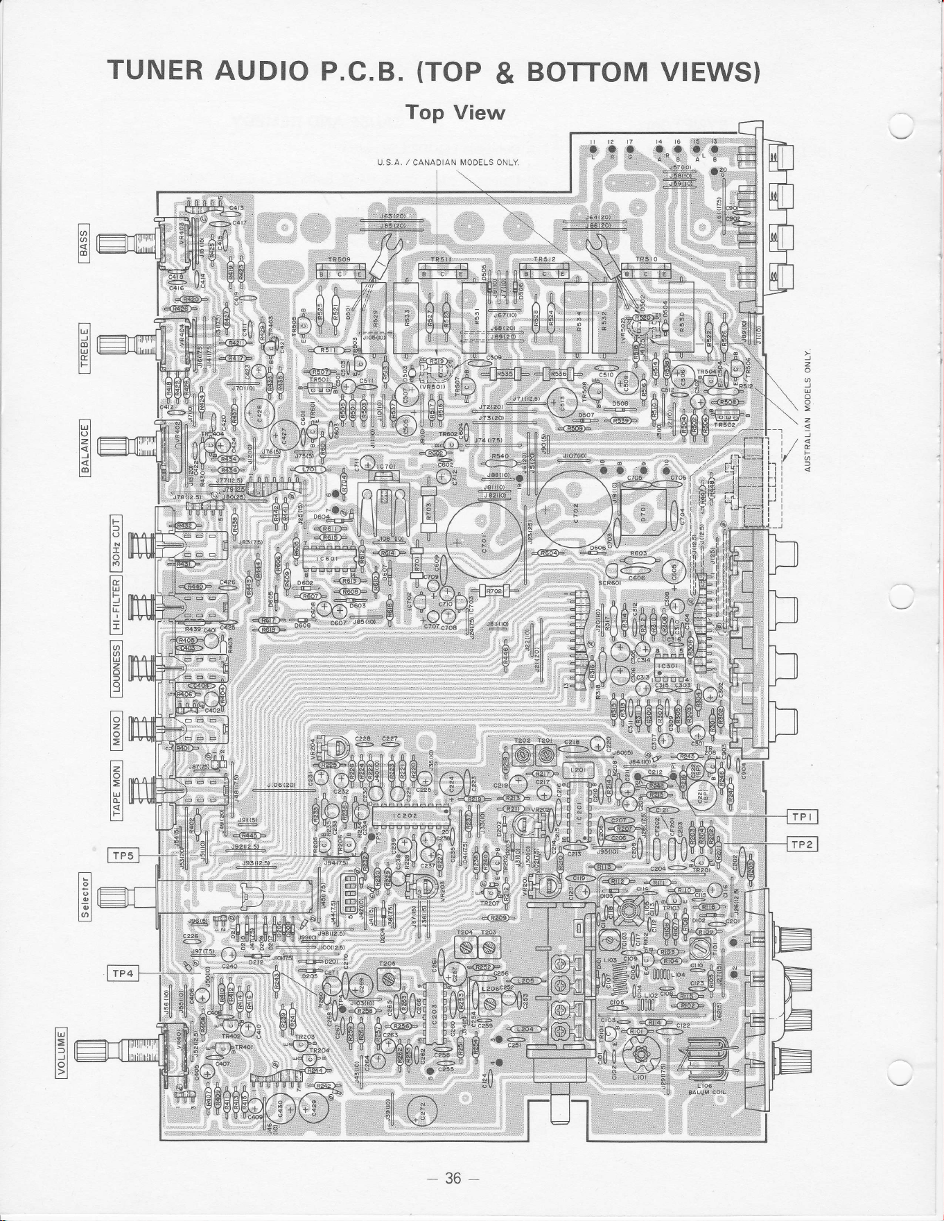
TUNER
AUDIO
P.C.B.
(TOP
&
BOTTOM VIEWS)
Top
View
tEt
lrl
lol
t-t
lTl
lol
trl
ta
lul
I1
l+l
lrl
l;t
lol
lul
lzl
lol
lll
E]
tJ
lzl
lo
E]
EI
lol
t>t
l-l
lIl
t<t
Lrl
-36
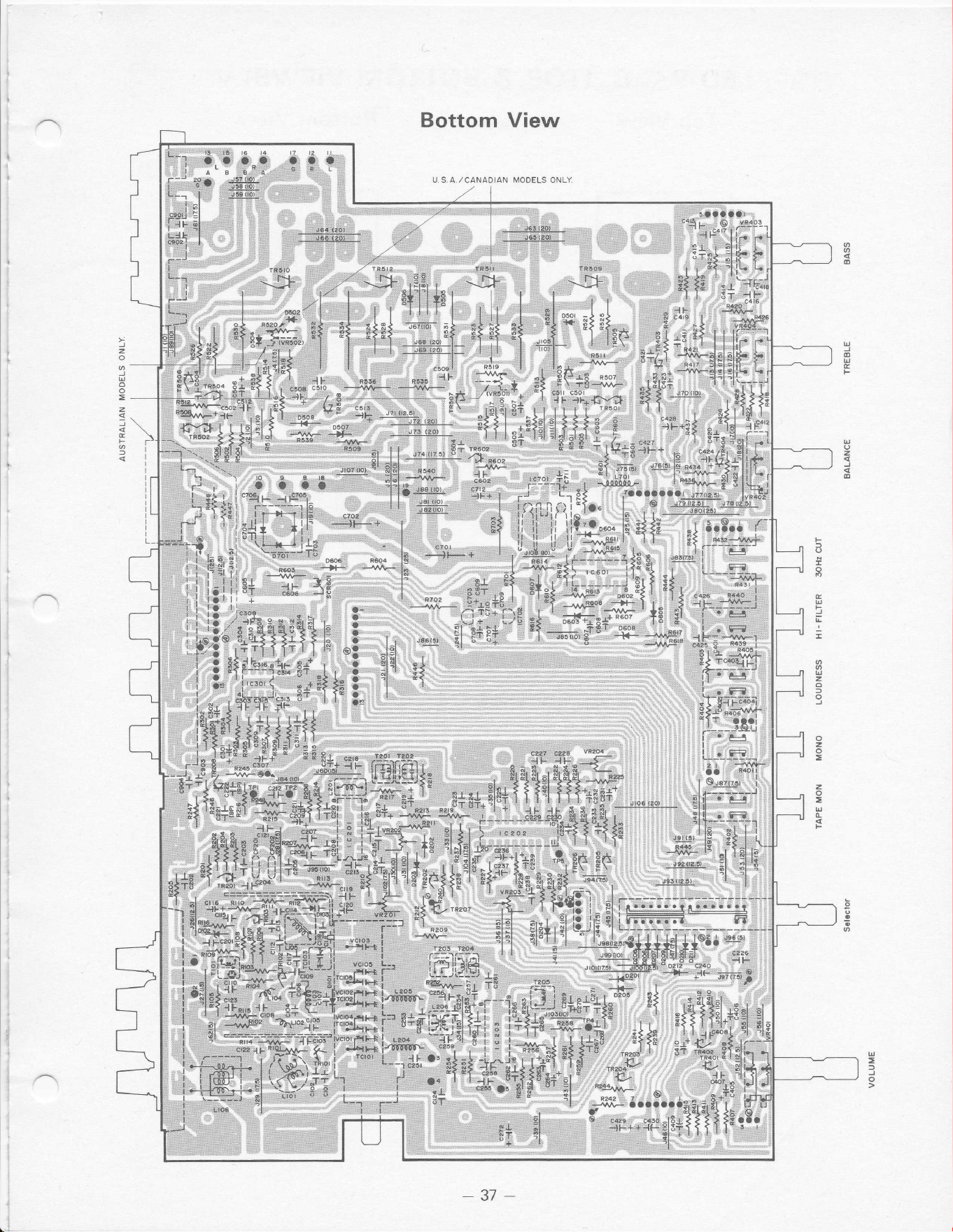
Bottom View
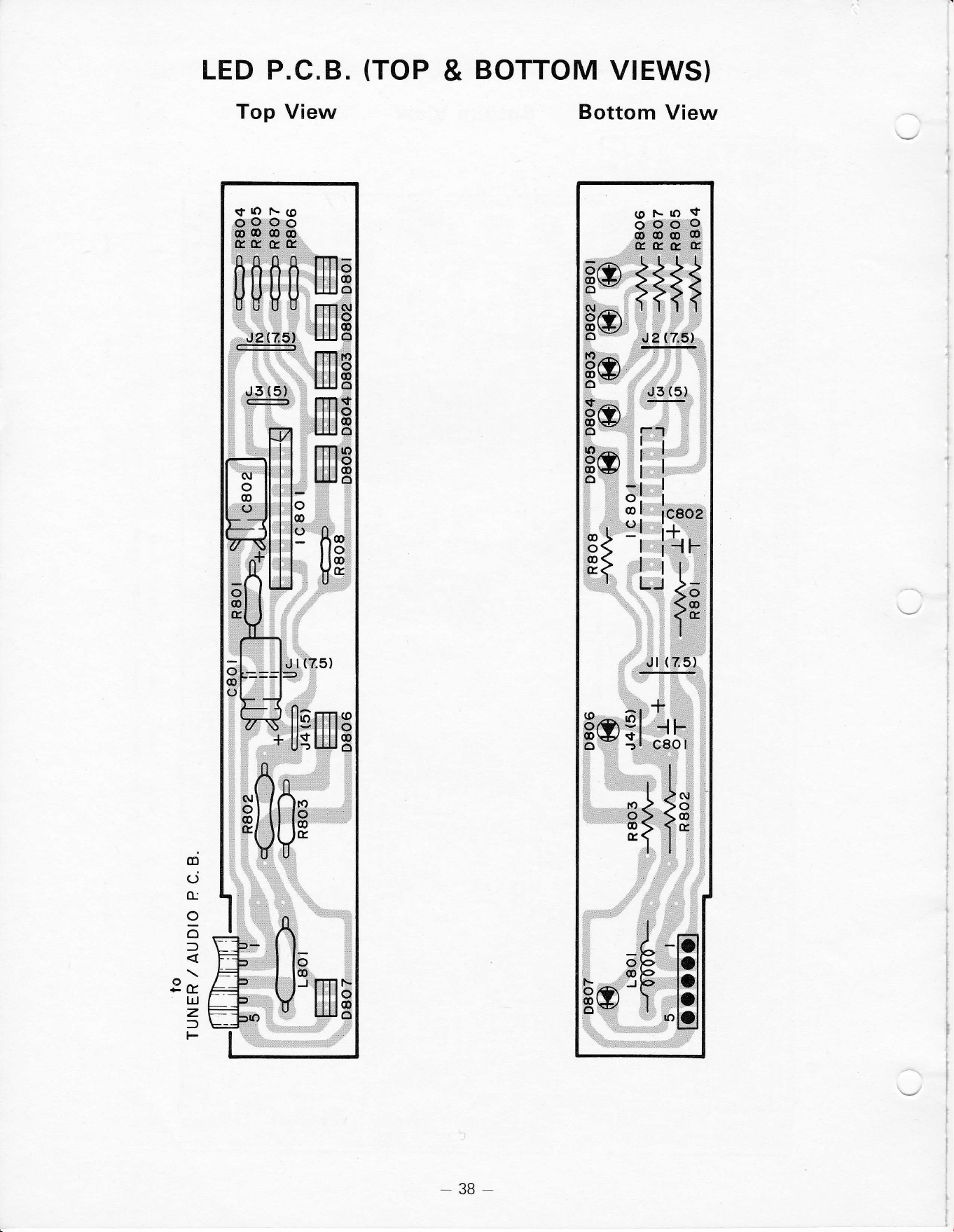
LED P.C. B.
Top View
(TOP
&
BOTTOM
VIEWS)
Bottom
View
tri
(J
Oi
o
d
f
Ps
ul
z
f
F
3B
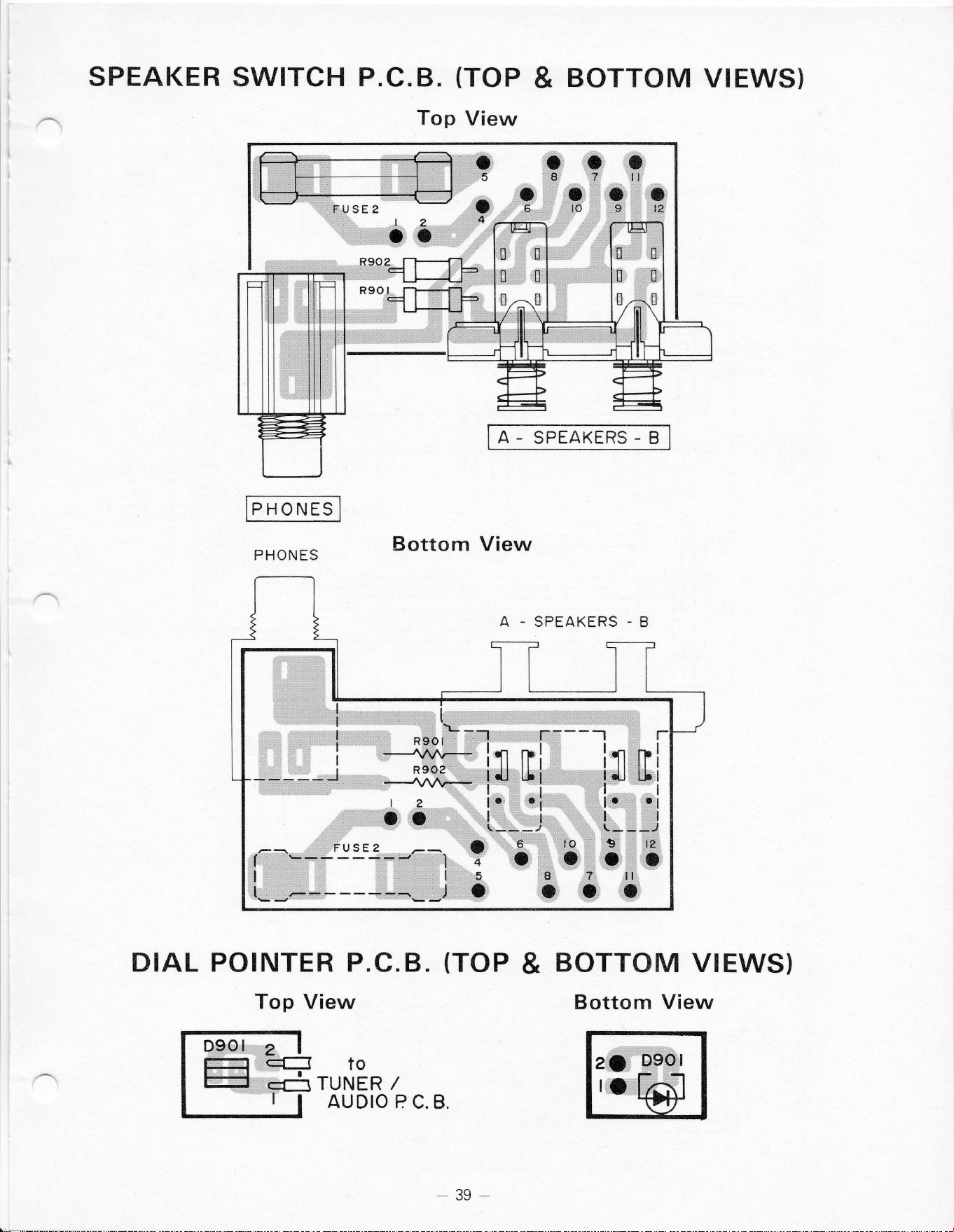
SPEAKER
SWITCH P.C.B.
(TOP
&
BOTTOM
VIEWS}
Top
View
PHONES
Bottom View
DIAL
POINTER
P.C-8.
(TOP
&
BOTTOM
VIEWS}
Bottom
ViewTop View
D9,Ol:
E-
H
to
TUNER /
AU
DIO
P
C. B.
SPEAKERS
2.
I
'
I
&c3
39-
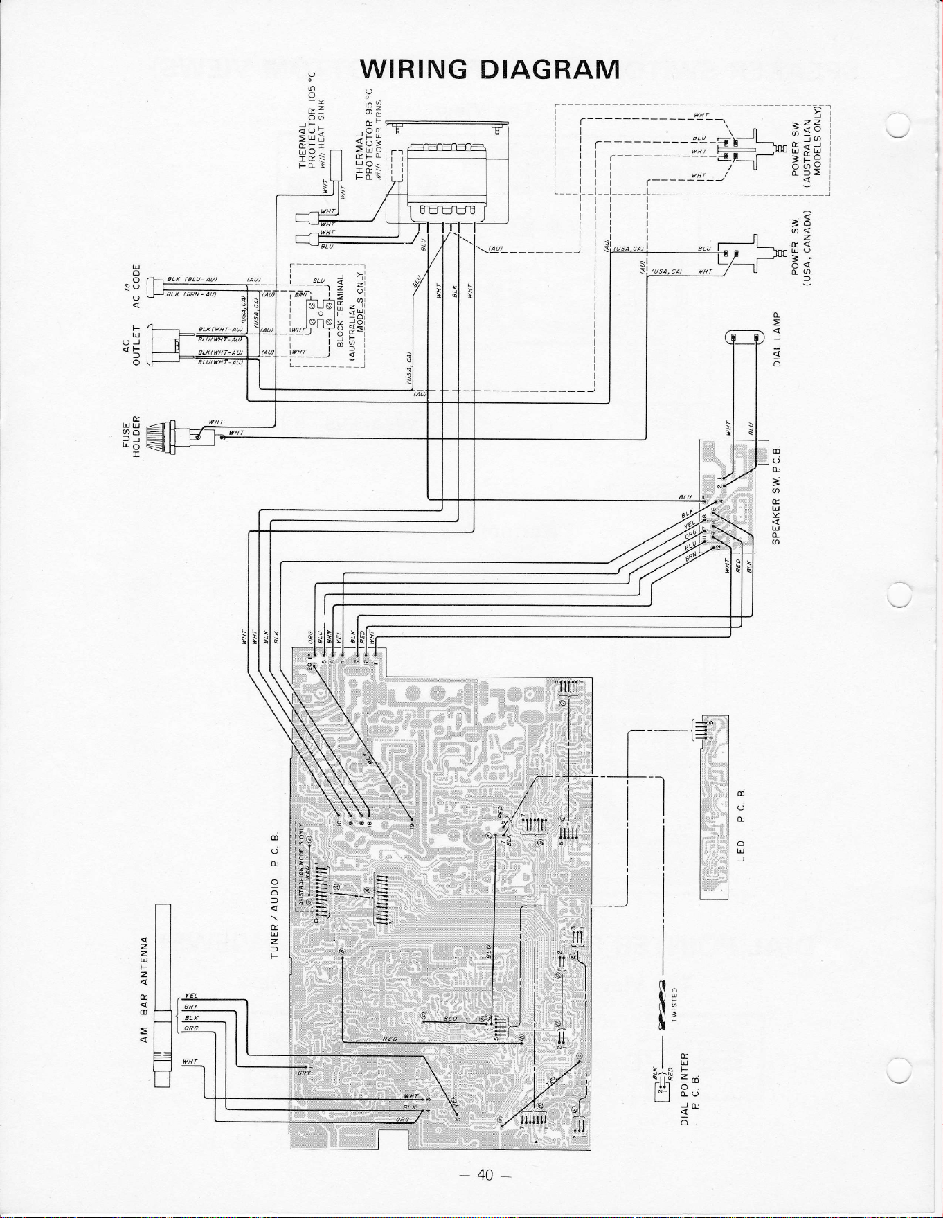
I
WIRING DIAGRAM
*Ht
\
-\
_e1" _=h_
vHr +
---:4
i
i
-i-
luHrl
i r--------
_t____
L___-_
rt
ll
II
ll
ll
-lj
I
r--
il
rl
I
lil
lll
tt
ll
t_
I
t_
lr
rl
lt
ll
tl
rl
_______J
I
I
I
I
I
I
I
I
I
I
I
I
I
I
I
I
I
________J
u
oq
oF
t'
.oE
<t.>
>;6
&FL
uos
F[:
o
o
o
e.Z
O@
JF.
<o!
=Uil
fi5:
Itti-
FC
r
-'-a
I
t 4)
g
PH
i
3 E= i
<l
I
.a
=a
6<
z
tr<
UO
]-
o<
Io
3
)ff
o
=
J
J
o
o
tu
i
a
&
U
Y
u
C
a
U
o
o
.Po
F
u
OJ
<F
l
o
E
UU
oo
ll
LO
I
ft
o
Oi
o
u
)
i
_l
o
.t
ft
o
o
f
tt
U
z
l
F
o
il3
L
lu
?Gt 3'
l*-l
r.
=*
.l
=ll
:ll
:H
tl
r
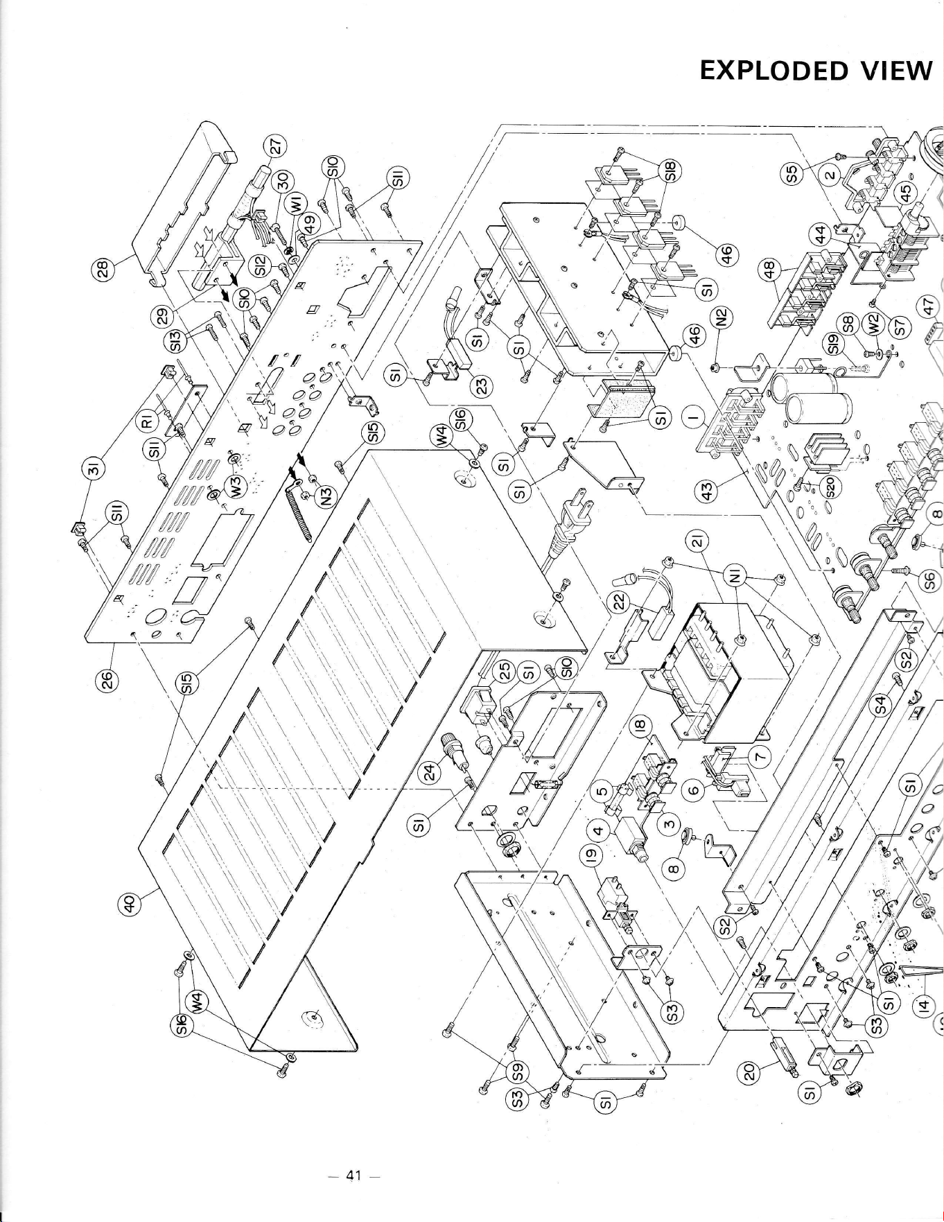
EXPLODED
VIEW
\€5
dL
w-.\
--Y(o
\*
n)/
o
/o
/
OKI
\qZ
h
_41
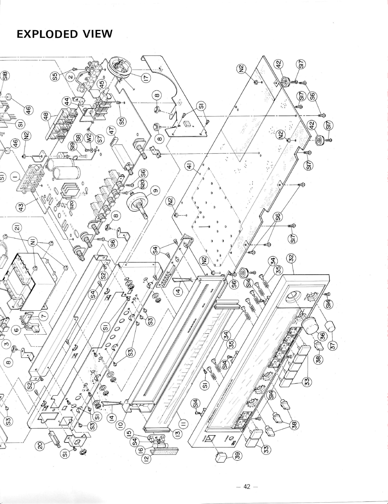
EXPLODED
VIEW
@\
\a)
r
i-ry
E\
+
'./c\
J- \$/
/-
-\-<n)
=
/ft\
-
^\z)
\ /@\r
\ \$i /
\-ft/v I
7tr\. L
/ r
r!)__F
0
\.0
'\00
\o
t
o./
0
\.
,o/
/Q\
\rol
favr\
,J
P,
qw/
&! /,
q'@
)q
x
u
/no\
\(r/
\-
,)
,)
q
-42
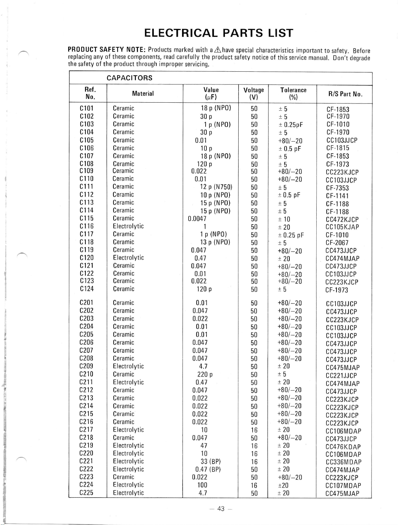
ELECTRICAL
PARTS LIST
PRODUCT
SAFETY
NOTE: Products marked
with aAhave
special
characteristics important
t0
safety. Before
replacing
any of these components,
read
carefully the
product
safety
notice
of
this service manual.
Don't
degrade
the
safety
of
the
product
through improper
servicing.
CAPACITORS
Bef
.
No.
Material
Value
furF)
Voltage
(v)
Tolera
nce
(%l
B/S
Part
No.
c
101
c102
c1 03
c 104
c
105
c 106
c
107
C 1OB
c 109
c110
c111
cl12
c1
13
c114
c115
c116
c117
c11B
c119
c120
c121
c122
c123
c124
c201
c202
c203
c204
c205
c206
c207
c20B
c209
c210
c211
c212
c213
c214
c215
c21 6
c217
C21B
c219
c220
c221
c222
c223
c224
c225
Ceramic
Ceramic
Ceramic
Ceramic
Ceramic
Ceramic
Ceramic
Ceramic
Ceramic
Ceramic
Ceramic
Ceramic
Ceramic
Ceramic
Ceramic
E lectro lytic
Ceramic
Ceramic
Ceramic
Electrolytic
Ceramic
Ceramic
Ceramic
Ceramic
Ceramic
Ceramic
Ceramic
Ceramic
Ceramic
Ceramic
Ceramic
Ceramic
E lectrolytic
Ceramic
Electrolytic
Ceramic
Ceramic
Ceramic
Ceramic
Ceramic
Electrolytic
Ceramic
Electrolytic
Electrolytic
Electrolytic
Electrolytic
Ceramic
Electrolytic
Electrolytic
18
p
(NP0)
3op
1
P
{NP0)
3op
0.01
1o
p
18
p
(NP0)
120
p
0.022
0.01
12
p
(N750)
10
p
(N
P0)
l5
P
(NPo)
15
p
(NP0)
0,0047
1
1
p (NPO)
13
P
(NPo)
0.047
0.47
0.047
0.01
0.022
120
p
0.01
0.047
0.022
0.0 r
0.01
0.047
0.047
0.047
4.7
220
p
0.47
0.047
0.022
0.422
0.022
0.022
10
0.047
47
10
33
(BP)
0.47
(BP)
0.022
100
4.1
50
50
50
50
50
50
50
50
50
50
50
50
50
50
50
50
50
50
50
50
50
50
50
50
50
50
50
50
50
50
50
50
50
50
50
50
50
50
50
50
16
50
16
16
16
50
50
16
50
t5
r5
t
0.25p F
r5
+B0i
-20
t
0.5
pF
t5
t5
+80/-20
+B0l-20
t5
r
0.5
pF
t5
15
t
10
t20
t
0.25
pF
t5
+80/-20
t20
+80/-20
+80/-20
+80/-20
t5
+80/-20
+80/-20
+80/-20
+801-20
+B0l-20
+80/-20
+B0l-20
+80/-20
t20
t5
t20
+80/-20
+80/-20
+80/-20
+80/-20
+801-20
t20
+80/-20
t20
t20
t20
t20
+80/-20
t20
t20
cF-1
853
cF-1
970
cF.1010
cF-1 970
CCl()3JJCP
CF-1815
cF-1
853
cF-1 973
CC223KJCP
CC 1
()3JJ
CP
cF-7353
cF-I141
cF-1 1
88
CF-1 I BB
cc472KJCP
CC 1
05 KJAP
cF-1010
cF.2067
CC473JJCP
CC474MJAP
CC473JJ CP
CCl()3JJCP
CC223KJCP
cF-1
973
CClO3JJCP
C C473JJCP
CC223KJ
CP
cc103JJCP
CClt)3JJCP
CC473JJ
CP
C
C473JJ CP
C C473JJ
CP
CC475MJAP
cc221JJCP
CC474MJAP
C C473JJ
CP
CC223KJ CP
CC223KJ
CP
CC223KJCP
C C223 KJ
CP
CCl 06MDAP
CC473JJ
CP
CC476
K
DAP
CC1
06MDAP
CC336M DAP
CC474MJAP
CC223
KJ CP
CC1
()TMDAP
CC475MJAP
43_
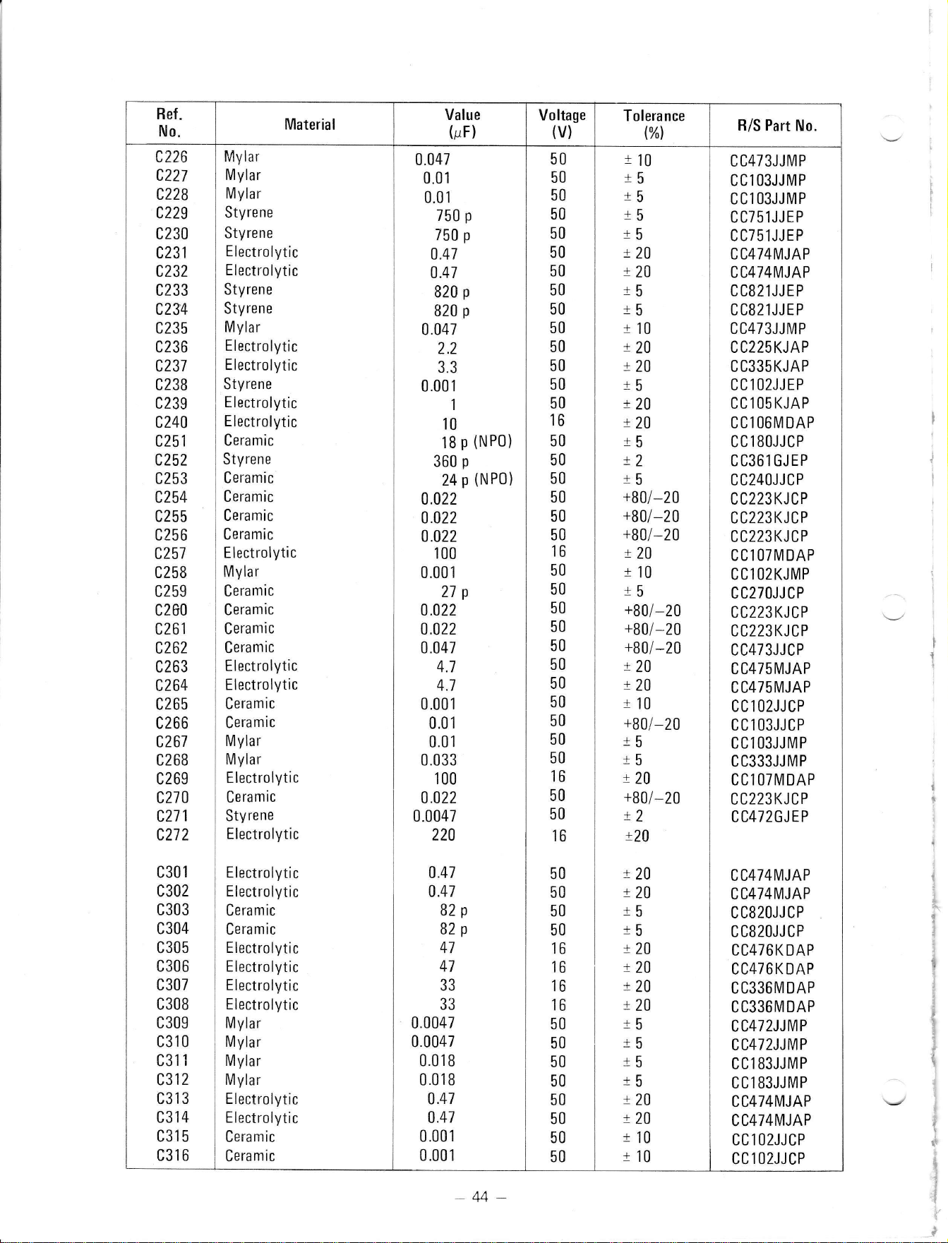
Ref
.
No.
Material
Value
furF)
Voltage
(v)
Tolera nce
(%l
R/S Part
No.
c226
c227
c22B
c229
c230
c231
c232
c233
c234
c235
c236
c237
C238
c239
c240
c251
c252
c253
c254
c255
c256
c257
c25B
c259
c260
c261
c262
c263
c264
c265
c2 66
c261
C268
c269
c270
c271
c272
c301
c302
c303
c304
c305
c306
c307
c308
c309
c310
c31
1
c312
c313
c314
c31 5
c31
6
Mylar
Mylar
Mylar
Styrene
Styrene
Electrolytic
E
lectrolytic
Styrene
Styrene
Mylar
E
lectrolytic
E
lectrolytic
Styrene
E
lectrolytic
Electrolytic
Ceramic
Styrene
Ceramic
Ceramic
Ceramic
Ceramic
Electrolytic
Mylar
Ceramic
Ceramic
Ceramic
Ceramic
E
lectrolytic
Electrolytic
Ceramic
Ceramic
Mylar
Mylar
E
lectrolytic
Ceramic
Styrene
Electrolytic
E lectrol
ytic
Electrolytic
Ceramic
Ceramic
Electrolytic
E lectrolytic
Electrolytic
E
lectrol
ytic
Mylar
Mylar
Mylar
Mylar
E lectrolytic
E lectrolytic
Ceramic
Ceramic
0.041
0.01
0.01
750
p
750
p
0.47
4.47
820
p
820
p
0.047
2.2
3.3
0.001
1
10
1B
p
(NP0)
360
p
24
p
(N
P0)
0.022
0.022
0.022
100
0.00 1
27p
0.022
0.022
0.047
4.7
4.7
0.001
0.01
0.01
0.033
100
0.022
0.0047
220
0.47
0.47
B2
82
47
47
33
33
0.0047
0.0047
0.018
0.018
0.47
0.47
0.001
0.001
p
p
50
50
50
50
50
50
50
50
50
50
50
50
50
50
16
50
50
50
50
50
50
16
50
50
50
50
50
50
50
50
50
50
50
16
50
50
16
50
50
50
50
16
16
16
16
50
50
50
50
50
50
50
50
r10
t5
r5
t5
t5
x20
t20
r5
t5
t10
t20
t20
t5
t20
t20
t5
tZ
t5
+80/-20
+80/-20
+80/-20
x20
t
10
t5
+80/-20
+80/-20
+80/-20
x20
r20
r
10
+80/-20
t5
r5
t20
+80/-20
t2
t20
t20
t20
t5
t5
r20
t20
t20
t20
t5
t5
t5
t5
t20
t20
t
10
t10
CC473JJMP
CClO3JJMP
CC
l
O3JJMP
CCT5IJJEP
CC751JJEP
CC474MJAP
CC474MJAP
CC821JJEP
CC821JJEP
CC473JJMP
CC225KJAP
C C335KJAP
CC 1 O2JJ
EP
CClOSKJAP
CC1 06MDAP
CC
1
SOJJCP
CC361 GJEP
CC24()JJCP
CC223
KJCP
CC223
KJCP
CC223
KJCP
CC1
()TMDAP
CCl 02KJMP
C C27OJJ CP
C C223
KJ
CP
CC223 KJCP
CC473JJCP
CC475MJAP
CC475MJAP
CC 1 O2JJCP
CC 1
O3JJ CP
CCl()3JJMP
CC333JJMP
CC1
()TMDAP
CC223
KJCP
C C472GJ
E P
CC474MJAP
CC474MJAP
C CB2()JJ CP
C
C82OJJ CP
CC476 K DAP
CC476KDAP
CC336MDAP
CC336MDAP
C C472JJM
P
CC472JJMP
CCl83JJMP
CC183JJMP
CC474MJAP
CC474MJAP
CC 1 O2JJ
CP
CC
1 OzJJ
CP
t
t
t
I
?
I
1
,1
il'
?
M
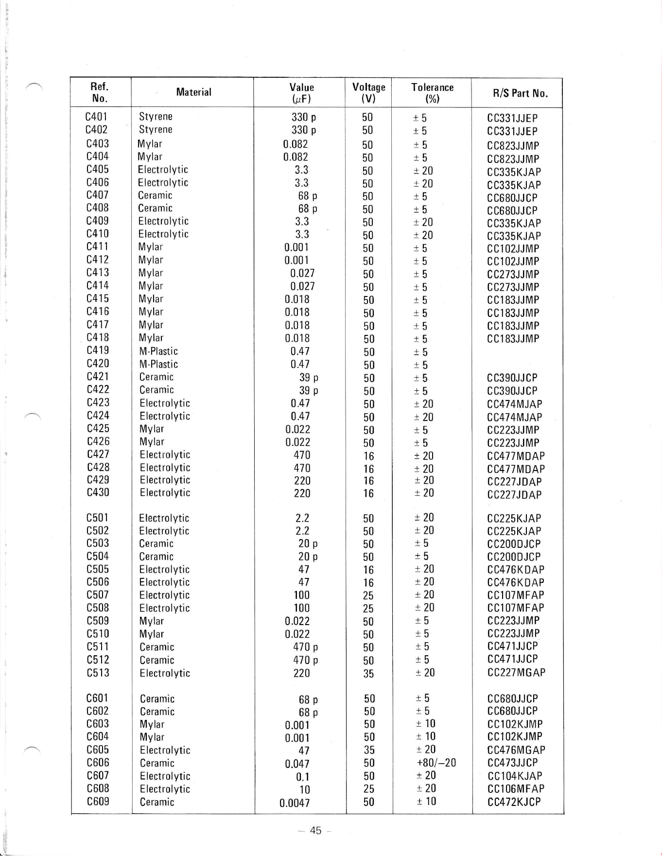
Ref
.
No.
Material
Value
tuF)
Voltage
(v)
To lera nce
l%l
R/S Part
No.
c401
c402
c403
c404
c405
c406
c407
C4OB
c409
c410
c411
c412
c41 3
c414
c41 5
c41 6
c417
c41B
c419
c420
c421
c422
c423
c424
c425
c426
c421
c428
c429
c430
c501
c502
c503
c504
c505
c506
c507
c50B
c509
c510
c51
1
c512
c513
c60l
c602
c603
c604
c605
c606
c607
c608
c609
Styrene
Styrene
Mylar
Mylar
Electrolytic
E lectrolytic
Ceramic
Ceramic
Electrolytic
Electrolytic
Mylar
Mylar
Mylar
Mylar
Mylar
Mylar
Mylar
Mylar
M-Plastic
M-Plastic
Ceramic
Cerarnic
Electrolytic
Electrolytic
Mylar
Mylar
Electrolytic
Electrolytic
Electrolytic
Electrolytic
Electrolytic
Electrolytic
Ceramic
Ceramic
E lectrolytic
Electrolytic
Electrolytic
E lectrolytic
Mylar
Mylar
Ceramic
Ceramic
Electrolytic
Ceramic
Ceramic
Mylar
Mylar
Electrolytic
Ceramic
Electrolytic
Electrolytic
Ceramic
330
p
330
p
0.082
0.082
J.J
3.3
68p
68p
3.3
3.3
0.001
0.001
0.027
0.027
0.018
0.018
0.018
0.018
0.47
0.41
39p
39p
0.47
0.47
0.022
0.022
470
470
220
220
2.2
2.2
2op
2op
47
41
100
100
0.022
0.022
470
p
470
p
220
68p
68p
0.001
0.001
47
0.047
0.1
10
0.0047
50
50
50
50
50
50
50
50
50
50
50
50
50
50
50
50
50
50
50
50
50
50
50
50
50
50
16
16
16
16
50
50
50
50
16
16
25
25
50
50
s0
50
35
50
50
50
50
35
50
50
25
50
t5
t5
t10
t
10
t20
+80/-20
t20
:.20
t10
t5
t5
t5
r5
t20
x20
t5
t5
x20
t20
i5
t5
t5
t5
t5
t5
t5
r5
+6
t5
r5
t5
x20
t20
t5
t5
t20
t20
t20
t20
t20
t20
t5
t5
x20
t20
t20
r.20
t5
t5
t5
t5
t20
CC33lJJEP
CC33lJJEP
GCB23JJ
M
P
CCB23JJMP
CC335KJAP
CC335KJAP
CC6BOJJ CP
cc680JJCP
CC335KJAP
CC335KJAP
CCl
O2JJMP
CCIO2JJMP
CC273JJMP
C C273JJ M
P
CCl B3JJ MP
CC183JJMP
CCIB3JJMP
CCl B3JJMP
C
C39()JJ
CP
cc39oJJ
CP
CC474MJAP
CC474MJAP
C C223JJ M
P
C C223JJ M
P
CC477MDAP
CC477MDAP
CC227JDAP
CC227JDAP
CC225KJAP
CC225KJAP
CC20ODJCP
CC20ODJCP
CC476KDAP
CC476K
DAP
CCl
()TMFAP
CCl
OTMFAP
CC223JJMP
CC223JJMP
c c471 JJ CP
c c47
lJJ
CP
CC227MGAP
CC6B()JJCP
cc68()JJCP
CCl02KJMP
CCl 02KJMP
CC476MGAP
C C473JJ CP
cc 1 04KiAP
CCI 06M
FAP
cc472KJ CP
_45_
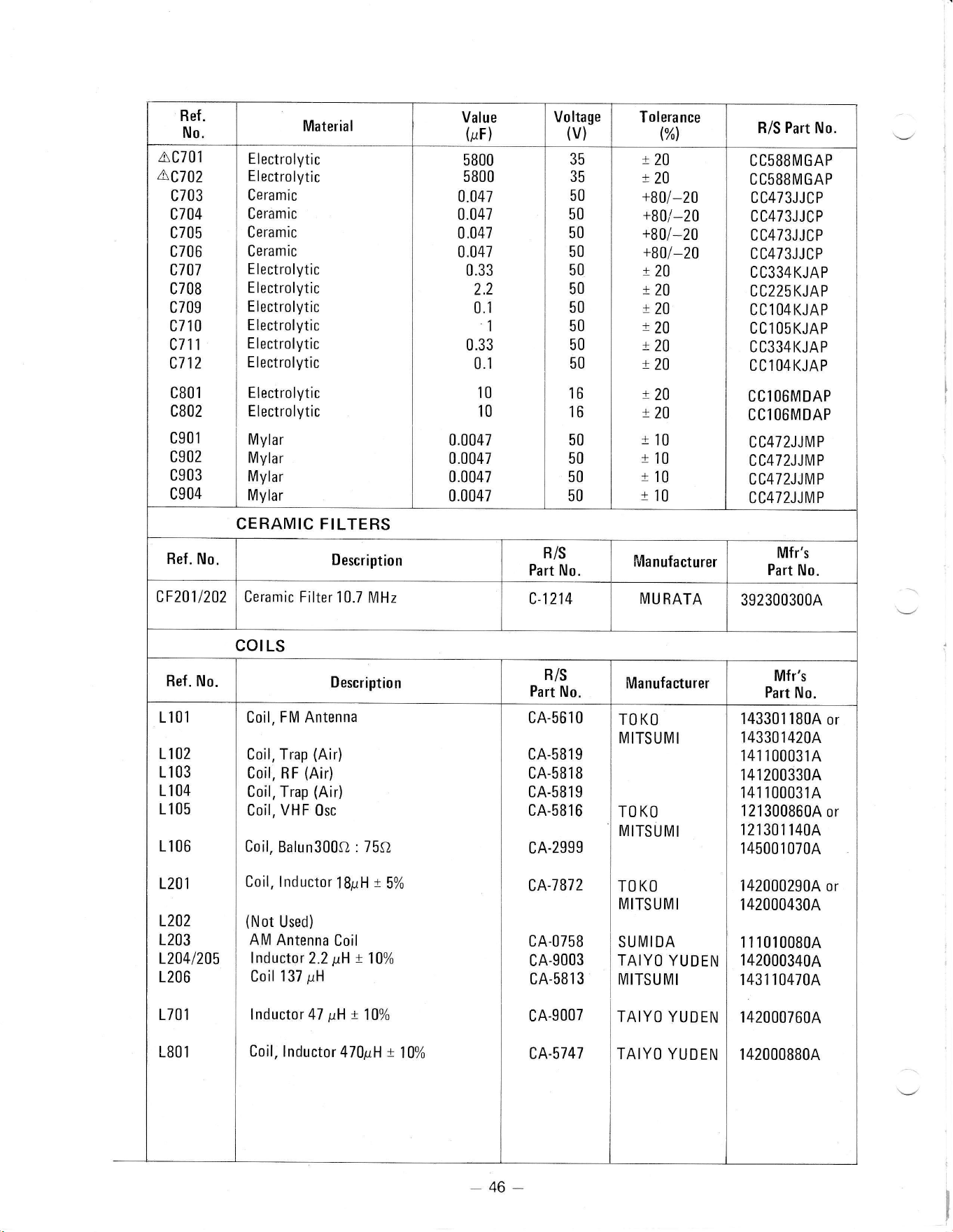
Ref
.
No.
Material
Value
(pF)
Voltage
(v)
Tolera nce
$t
B/S
Part
No.
AC7O1
ACl02
c703
c704
c705
c706
ct07
C7 t]B
c709
c710
cl
11
c7
12
CBOl
c802
c901
c902
c903
c904
E lectrolyti
c
E I
ectrolytic
Ceramic
Ceramic
Ceramic
Ceramic
Electrolytic
Electrolytic
Electrolytic
E I ectrol
yti
c
Electrolytic
E
lectrolytic
Electrolytic
E lectrolytic
Mylar
Mylar
Mylar
Mylar
5800
5800
0.047
0.047
0.047
0.047
0.3
3
2.2
0.1
1
0.33
0.1
't0
10
0.0047
0.0047
0.0047
0.0047
35
35
50
50
50
50
50
50
50
50
50
50
16
16
50
50
50
50
r20
r20
+80/-20
+80/-20
+80/-20
+B0l-20
+20
t20
t20
!20
:.20
t20
+20
t20
t
10
t
10
t
10
r
10
CCsBSMGAP
CCSBSMGAP
CC473JJCP
CC473JJCP
CC473JJCP
CC473JJCP
CC334KJAP
C C225 KJAP
CC 1 04KJAP
CC 105
KJAP
CC334KJAP
CC 1
04KJAP
CC1 06MDAP
CC1
06MDAP
C C47 2JJM P
C C472JJM
P
CC472JJMP
CC472JJMP
CERAMIC FILTERS
Ref. No.
Deseription
H/S
Part No.
Manufacturer
Mfr's
Part
No.
cF2011202 Ceramic Filter
10.7
MHz
c-l214
MU
RATA
392300300A
COILS
Ref. No.
Description
R/S
Part
No.
Manufacturer
Mfr's
Part
No.
L1 01
11 02
11 03
11 04
11 05
11
06
L201
L202
1203
L2041205
1206
1701
LB(] 1
Coil, FM Antenna
Coil,
Trap
(Air)
Coil,
RF
(Air)
Coil, Trap
(Air)
Coil,
VHF
0sc
Coil,
Balun300O
: 75sl
Coil, lnductor
lBpH
r
5%
(Not
Used)
AM
Antenna
Coil
lnductor
2.2
pH x
10%
Coil
137
pH
lnductor 47
pH t
10o/o
Coil, lnductor
470pH
t
10%
cA.5610
cA-581 I
CA-s818
cA-s819
cA-s816
cA-2999
cA-1872
CA-0758
cA-9003
cA-5813
cA-9007
cA-5747
TO KO
MITSUMI
TO
KO
MITSUMI
TO
KO
MITSUMI
SUMI DA
TAIYO
YUDEN
MITSUMI
TAIYO YUDEN
TAIYO YUDEN
143301 I80A
or
1 4330 1 420A
141100031A
1 4 1
200330A
141 100031A
121300860A
or
121301
140A
1
4500
1
070A
1420002904
or
1
42000430A
1110100804
1 42000340A
143i 10470A
1 42000760A
1
42000880A
46-
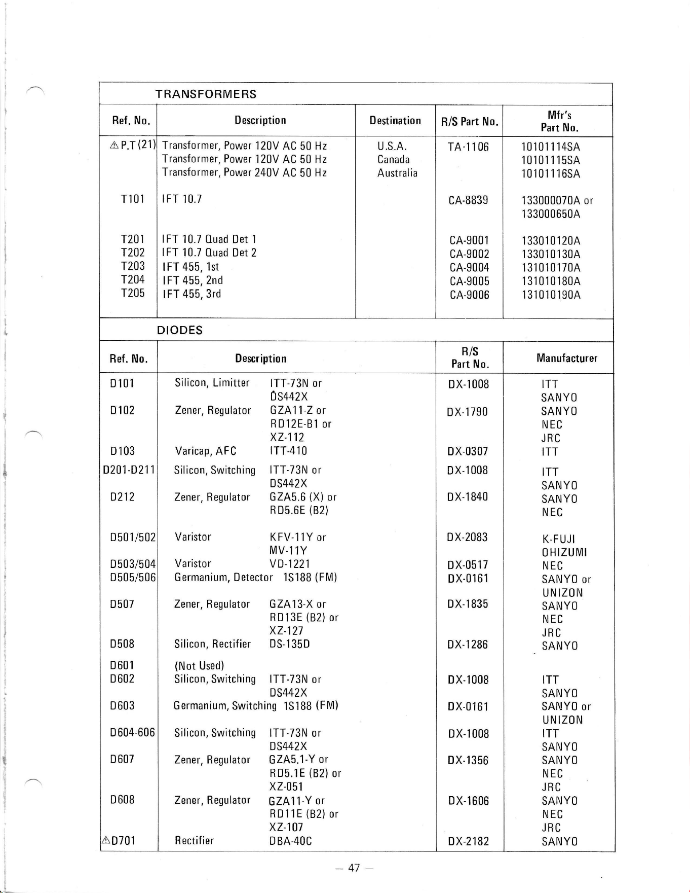
TRANSFORMERS
Ref. No.
Description
D estination
R/S Part No.
Mfr's
Part No.
A
P.T
(21
T1 01
T201
T202
T203
T204
T205
Transformer, Power
120V
AC 50
Hz
Transformer, Power
i20V
AC 50
Hz
Transformer,
Power
240V
AC 50
Hz
IFT
'10.7
0uad Det
1
IFT
10.7
Ouad Det 2
I FT 455,
1st
I FT
455, 2nd
IFT
455,3rd
10.7
IFT
U.S.A.
Canada
Australia
TA-1106
CA.BB39
cA-9001
cA-9002
cA-9004
cA-9005
cA-9006
10101 1 14SA
10101 1 15SA
1010't1165A
133000070A
or
1 33000650A
133010120A
1330i0130A
131010170A
131010180A
131010190A
DIODES
Hef. No.
Description
R/S
Part
No.
Manufacturer
D 101
D 102
D
103
D201-D211
D212
D
50
1
/502
D503/504
D
505/506
D507
D508
D
601
D 602
0603
D604-606
D607
D 608
ADTOi
Silicon, Limitter
ITT-73N or
Ds++zx
Zener,
Regulator GZA|\-Z or
RD12E-B1
or
xz_112
Varicap, AFC
ITT-410
Silicon, Switching
ITT-73N or
DS442X
Zener, Regulator GZA5.6
(X)
or
RD5.6E
(82)
Varistor
Varisto r
G
ermanium,
KFV-1
1Y or
MV.11Y
vD.1221
Detector 1S1BB
(FM)
Zener, Regulator
GZA13-X
or
RD13E
(82)
or
xz_127
Silicon,Rectifier
DS-135D
(Not
Used)
Silicon, Switching
ITT-73N
or
DS442X
Germanium,
Switching
ISlBB
(FM)
Silicon,
Switching
ITT-73N or
DS442X
Zener, Regulator
GZA5.1-Y
or
R 05.1E
(82)
or
xz_051
Zener,
Regulator
GZA1l-Y
or
RD1
1E
(B2)
or
xz-107
R
ectif
ier
D
BA-40C
D X.1 OOB
DX-1790
DX-0307
D
X-1 OOB
DX-1840
DX-2083
D
X-0517
DX-0161
DX-1835
DX-1286
DX-1008
D X-0161
D
X-1
O(]B
DX-1356
D X-1606
DX-2182
ITT
SANYO
SANYO
NEC
JRC
ITT
ITT
SANYO
SANYO
NEC
K-F
UJ
I
O
HIZU MI
NEC
SANYO
or
UNIZON
SANYO
NEC
JRC
SANYO
ITT
SANYO
SANY0 or
UNIZON
ITT
SANYO
SANYO
NEC
JRC
SANYO
NEC
JRC
SANYO
-41
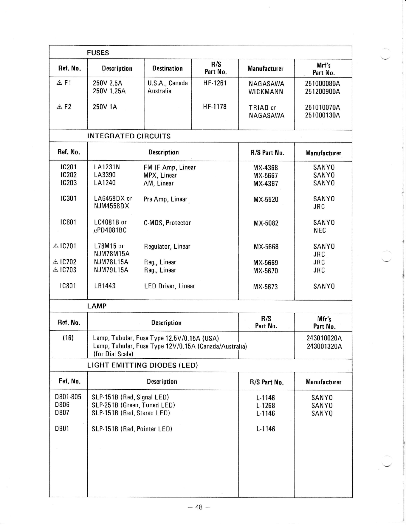
FUSES
Ref. No.
Description
Destination
R/S
Part No.
Manufacturer
Mrf's
Part
No.
AFl
AF2
250V 2.5A
250V
1.25A
250V 1A
U.S.A.,
Canada
Australia
H
F-l261
HF-lr78
NAGASAWA
WICKMANN
TRIAD
or
NAGASAWA
25 1 000080A
25 r 200900A
2510100704
251000130A
NTEGRATED
CIRCUITS
Ref. No.
Description
R/S Part
No.
Manufacturer
rc201
1c202
r
c203
r
c301
rc601
a
rc701
a
tc702
a
tc703
rc801
LA1231N
1A3390
1A1240
LA645BDX
or
NJM4558DX
LC4081B
or
pPD408
1
BC
178M15 or
NJM7BMl5A
NJM78L15A
NJM79L15A
LB 1 443
FM
lF Amp,
Linear
MPX,
Linear
AM, Linear
Pre
Amp, Linear
C-M0S,
Protector
Regulator,
Linear
Reg., Linear
Reg., Linear
LED
Driver, Linear
MX-4368
MX-5667
MX-4367
MX-5520
MX-5082
MX-5668
MX-5669
MX-5670
MX-5673
SANYO
SANYO
SANYO
SANYO
JRC
SANYO
NEC
SANYO
JRC
JRC
JRC
SANYO
LAMP
Ref. No.
Description
Ris
Part
No.
Mfr's
Part
No.
(16)
Lamp, Tubular, Fuse
Type
12.5V/0.15A
(USA)
Lamp,
Tubular, Fuse
Type 12Vl0.15A
(Canada/Austra
(for
Dial
Scale)
lia)
2430
1
0020A
243001320A
LIGHT EMITTING
DIODES
(LED)
Fef.
No.
Description
R/S Part
No.
Manufacturer
D801-805
D806
D807
D901
SLP-l51B
(Red,
Signal
LED)
SLP-2518
(Green,
Tuned LED)
SLP-l51 B
(Red,
Stereo
LED)
SLP-l51B
(Red,
Pointer
LED)
L-1 146
L.l 268
L-1 146
L-1 146
SANYO
SANYO
SANYO
-48-
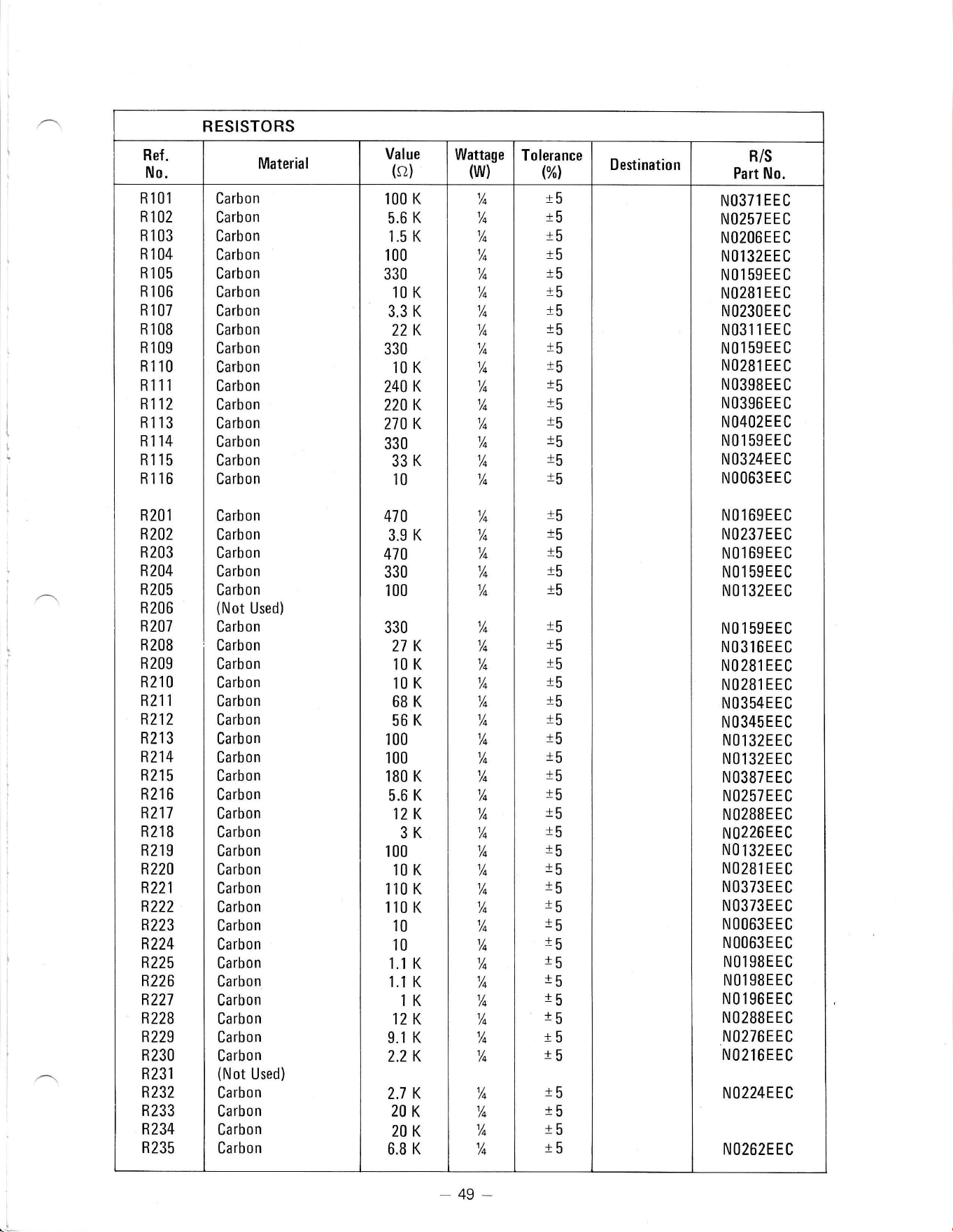
RESISTORS
Ref
.
No.
Material
Value
(o)
Wattage
(w)
Tolerance
(%l
Destinatio n
Bis
Part No.
R 101
R 102
R 103
R 104
R 105
R',t06
R
107
R
1OB
R 109
R110
R111
R112
R113
R114
R115
R116
R
201
R202
R203
R
204
B 205
R206
R207
R2OB
R209
R210
R21 i
R212
R21
3
R214
R2',t5
R21
6
R217
R21B
R
219
R220
R221
R222
R223
R224
R225
R226
R227
R228
R229
R230
R23
1
R232
R233
R234
R235
Carb
o n
Carbon
Carbon
Carbon
Carbon
Carbon
Carbon
Carbon
Carbon
Carbon
Carbon
Carbon
Carbon
Carbon
Carb
o n
Carbon
Carbon
Carb
o n
Carbon
Carbon
Carbon
(Not
Used)
Carbon
Carbon
Carbon
Carbon
Carb o
n
Carbon
Carbon
Carbon
Carbo
n
Carbon
Carbon
Carbon
Carbon
Carbon
Carbon
Carbon
Carb
o
n
Carbon
Carbon
Carbon
Carbon
Carbon
Carbon
Carbon
(Not
Used)
Carbon
Carbon
Carbon
Carbon
100
K
5.6
K
i.5 K
100
330
10 K
3.3
K
22K
330
10
K
240
K
220 K
270
K
330
33K
10
470
3.9
K
470
330
100
330
27K
10
K
10
K
68K
56K
100
100
180
K
5.6
K
12K
3K
100
10 K
i10 K
110 K
10
10
1.1 K
1.1 K
1K
12K
9.1
K
2.2 K
2.7 K
20K
20K
6.8 K
lo
To
lo
lo
1/
/4
,/o
,/o
lo
t/o
lo
To
lo
1/o
1/
/4
1/q
1/
/4
To
,/o
To
lo
lo
1/q
Tq
1/
/4
t/o
,/o
,/o
1/
/4
1/
/4
lo
,/o
lo
,/o
,/o
1/
/4
lo
To
1/
/4
lo
%
To
lo
To
lo
1/
/4
lo
Tt
To
1/
/4
t5
r5
t5
r5
r5
r5
15
15
r5
t5
r5
15
15
r5
t5
15
r5
15
l5
t5
l5
15
15
r5
r5
r5
15
15
r5
r5
t5
15
r5
r5
15
15
15
15
t5
+E
t5
15
t5
r5
15
15
15
15
15
N0371 EEC
N0257 E E
C
N0206E
E
C
N01
32EEC
N0159EEC
N0281
EEC
N()23()EEC
NO31 1
EEC
N(]159EEC
N0281
EEC
N(]398E
E C
N0396E E
C
NO4O2E
E
C
NO159EEC
N0324EEC
N0063EEC
NO169EEC
NO237EE C
N0169EEC
N()159EEC
N0 132EEC
N0159EEC
N0316EEC
N0281EEC
NO281
EEC
N
0354E
E
C
N0345EEC
NO132EEC
NO132EEC
N0387EEC
N0257 E E
C
NO2BBE
E
C
N0226EEC
NOl32EEC
N(]281EEC
N0373EEC
N0373EE
C
NO063EEC
N0063EEC
N01 98EEC
NO1 98EEC
NOl96EEC
N0
288EEC
NO276EEC
N0
21
6EE C
NO 224E
E
C
NO262EE
C
49-
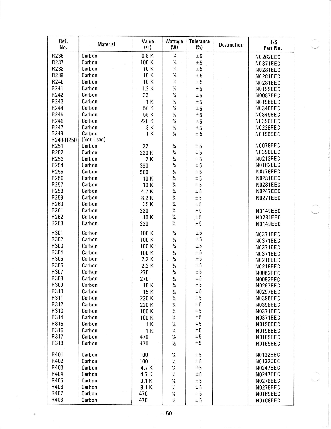
Ref
.
No.
Material
Value'
(o)
Wattage
(w)
Tolerance
%l
Destination
B/S
Part No.
R236
R237
R238
R239
R240
R241
R242
R243
R244
R245
R246
R247
R248
R249-R250
R
251
R252
R253
R254
R255
R256
R257
R25B
R259
R260
R26 1
R262
R263
R301
R302
R303
R304
R305
R306
R307
R3()B
R
309
R310
R31 1
R
312
R31
3
R31 4
R31
5
831
6
R31
7
R31
8
R401
R402
R403
R404
R405
R406
R407
R40B
Carbon
Carbon
Carbon
Carbon
Carbon
Carbon
Carbon
Carbon
Carbon
Carbon
Carbon
Carbon
Carbon
(Not
Used)
Carbon
Carbon
Carbon
Carbon
Carbon
Carbon
Carbon
Carbon
Carbon
Carbon
Carbon
Carbon
Carbon
Carbon
Carbon
Carbon
Carbon
Carbon
Carbon
Carbon
Carbon
Carbon
Carbon
Carbon
Carbon
Carbon
Carbon
Carbon
Carbon
Carbon
Carbon
Carbon
Carbon
Carbon
Carbon
Carbon
Carbon
Carbon
Carbon
6.8
K
100
K
10K
10K
10
K
1.2
K
33
1K
s6K
56K
220
K
3K
1K
22
220 K
2K
390
560
10K
10K
4.1 K
8.2
K
39K
220
10K
220
100 K
100
K
100
K
100
K
2.2 K
2.2 K
270
210
15K
15
K
220 K
220
K
100 K
100 K
1K
1K
470
470
100
100
4"7 K
4.7 K
9.1
K
9.1
K
470
470
To
1/o
/4
la
1/
1t
/4
1/
To
Yo
To
lo
lo
%
To
1/
/A
1/
1/
/4
Tq
lo
To
%
'/a
%
'/4
1t
/4
%
%
%
/4
To
Yo
%
ft
/4
%
Y4
Y4
/2
/2
To
/4
%
To
%
/4
%
%
t5
t5
t5
15
15
r5
15
t5
t5
15
15
r5
15
t5
l5
15
r5
t5
t5
t5
r5
t5
i5
t5
t5
t5
r5
t5
15
15
t5
t5
tb
t5
l5
15
15
t5
r5
15
t5
t5
r5
15
l5
15
15
r5
r5
t5
15
r5
N0
262EE
C
N0371EEC
N0281 EEC
N0281 EEC
NO28l
EEC
N0
199EEC
N0087EEC
N0196EEC
NO345EEC
N()345EEC
N0396EE
C
N0226EE
C
N0 1
96EEC
N0078EEC
N0396E
EC
N02t 3EE C
N0
1
62EE C
N(]l 76EE C
N0281
EEC
N()2BlEEC
N0247 E E
C
N0271 EEC
N0149EEC
NO281EEC
N0
149EEC
N0371
EEC
N0371
EEC
N0371
EEC
N0371
EEC
N021 6E
EC
Nt) 21 6E EC
N0082EEC
NO082E
EC
N0297EE
C
N0297EE
C
N0396E
EC
N0396EE
C
N0371 EEC
N0371
EEC
N()196EEC
N01
96EEC
N01 69EEC
N01
69EEC
N0
1
32EEC
N0
1 32EE
C
N0247EEC
N0247EEC
N0276EEC
NO276EEC
N0169EEC
N0169EEC
-50-
1
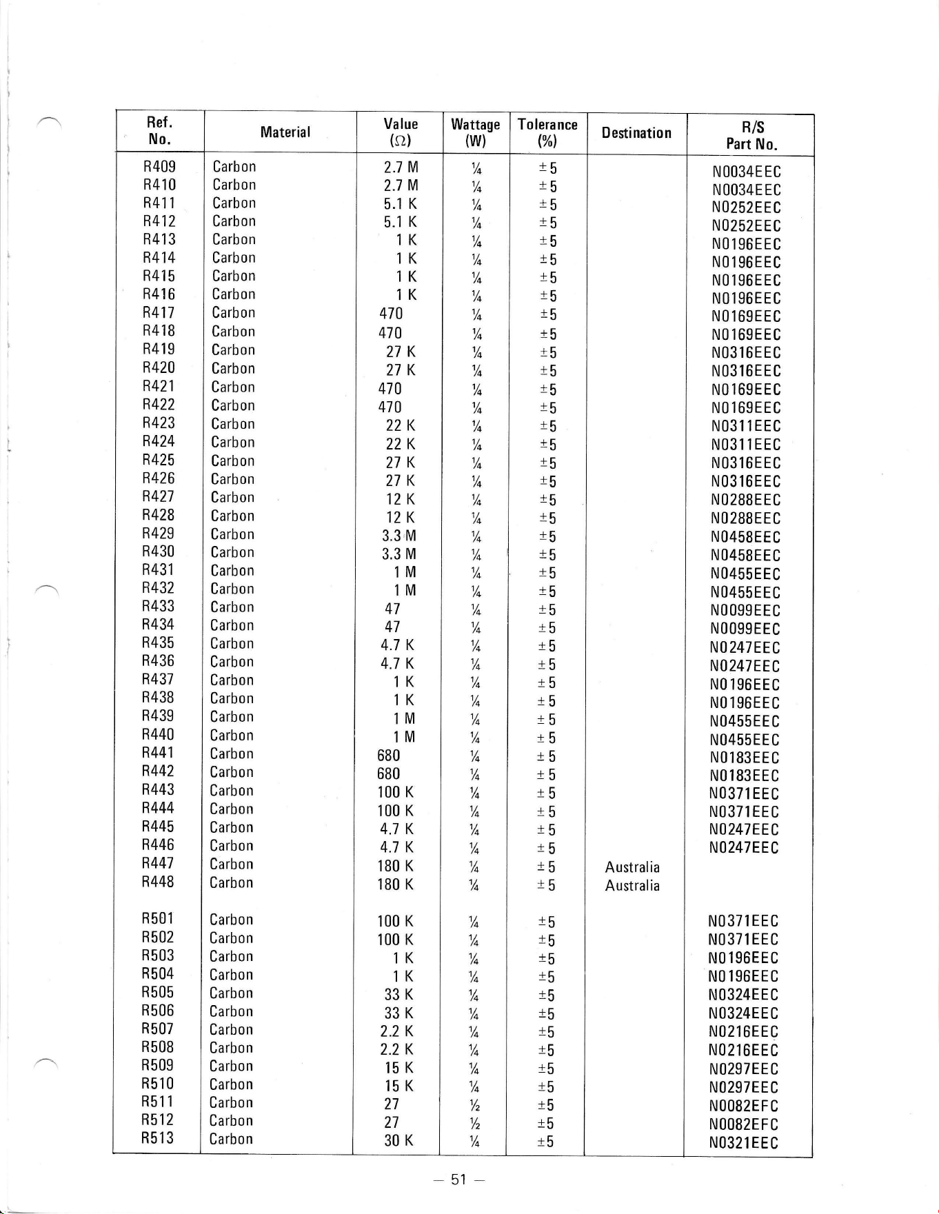
Ref .
No.
Material
Value
(sr)
Wattage
(w)
Tolera nce
%t
Destination
R/S
Part
No.
8409
R41
0
R41 1
R412
R41
3
R414
R4i5
R41
6
R417
R41B
R41
I
R420
R421
R422
R423
R424
R425
R426
R427
R42B
R429
R430
R43 1
R432
R433
R434
R435
R436
R437
R43B
R439
R440
R441
R442
R443
R444
R445
R446
R447
R44B
R501
R502
R 503
R
504
H
505
R
506
R507
R508
R
509
R510
R51
1
R512
R513
Carbon
Carbon
Carbon
Carb
o n
Carbon
Carbon
Carbon
Carb o
n
Carbon
Carbon
Carbon
Carbon
Carbon
Carb
on
Carbon
Carbon
Carbon
Carb
on
Carbon
Carbon
Carbon
Carbon
Carb
o
n
Carbon
Carbon
Carbon
Carbon
Carbon
Carbon
Carbon
Carbon
Carbon
Carbon
Carbon
Carbon
Carbon
Carbon
Carbon
Carbon
Carbon
Carbon
Carbon
Carbon
Carbon
Carbon
Carbon
Carbon
Carbon
Carbon
Carbon
Carb
o n
Carbon
Carbon
2.7
lli
2.7
ll
5.1
K
5.1
K
1K
1K
1K
1K
410
470
27K
2tK
470
410
22K
22K
27K
27K
12K
12K
3.3,M
3.3
M
1M
1M
47
41
4.1 K
4.7 K
1K
1K
1M
IM
680
680
100
K
100
K
4.7 K
4.7 K
1BO K
180 K
100
K
100
K
1K
1K
33K
33K
2.2 K
2.2
K
15
K
15K
21
27
30K
To
1/o
1/o
lo
lo
1/o
,/o
To
1/o
To
lo
lo
lo
,/o
lo
1/
/4
lo
,/o
Tq
t/o
1/o
t/o
1/
/4
,/o
Tq
1/
/4
,/o
1/q
%
To
Tq
't/
/4
lq
T+
t/o
1/q
To
lo
lo
,/a
lo
Yo
1/
/4
1/
/4
1A
lo
1/
/4
lo
To
lo
1/
/2
Y,
To
15
15
t5
r5
15
r5
15
15
15
15
r5
t5
15
15
r5
15
15
r5
t5
r5
r5
t5
r5
15
t5
r5
t5
r5
t5
t5
15
r5
15
t5
15
15
t5
t5
t5
t5
15
15
15
t5
t5
r5
t5
15
15
15
r5
t5
t5
A ustral ia
Australia
N O()34E
EC
N(]O34E EC
N0252EE
C
N0252EEC
Nt]l96EEC
NO196EEC
NO 1 96EEC
N0196EEC
NO169EEC
N0169EEC
N03t6EEC
N03 1 6EE C
N0
1
69EEC
NO
1
69EE C
NO31 1
EEC
NO31 1
EEC
N0316EEC
N0316EEC
NO288E E
C
N(] 288EE
C
NO4SBEE
C
N0458E
E
C
N0455E
E
C
N0455EEC
N00g9EEC
N0099EEC
N0247EEC
N0247EEC
N0 196EEC
NOl96EEC
N0455E E
C
N0455E E
C
NO183EEC
Nt)l83EEC
N0371EEC
N0371 EEC
N0247EEC
N0247EEC
N0371
EEC
N0371
EEC
NOl96EEC
N0 196EEC
N
0324E
E
C
N
0324E
E
C
N02
1
6EE C
N02
1
6EE C
N0297EE
C
N0297EEC
N0082E
F
C
N0082E
F
C
N0321 EEC
-51
-
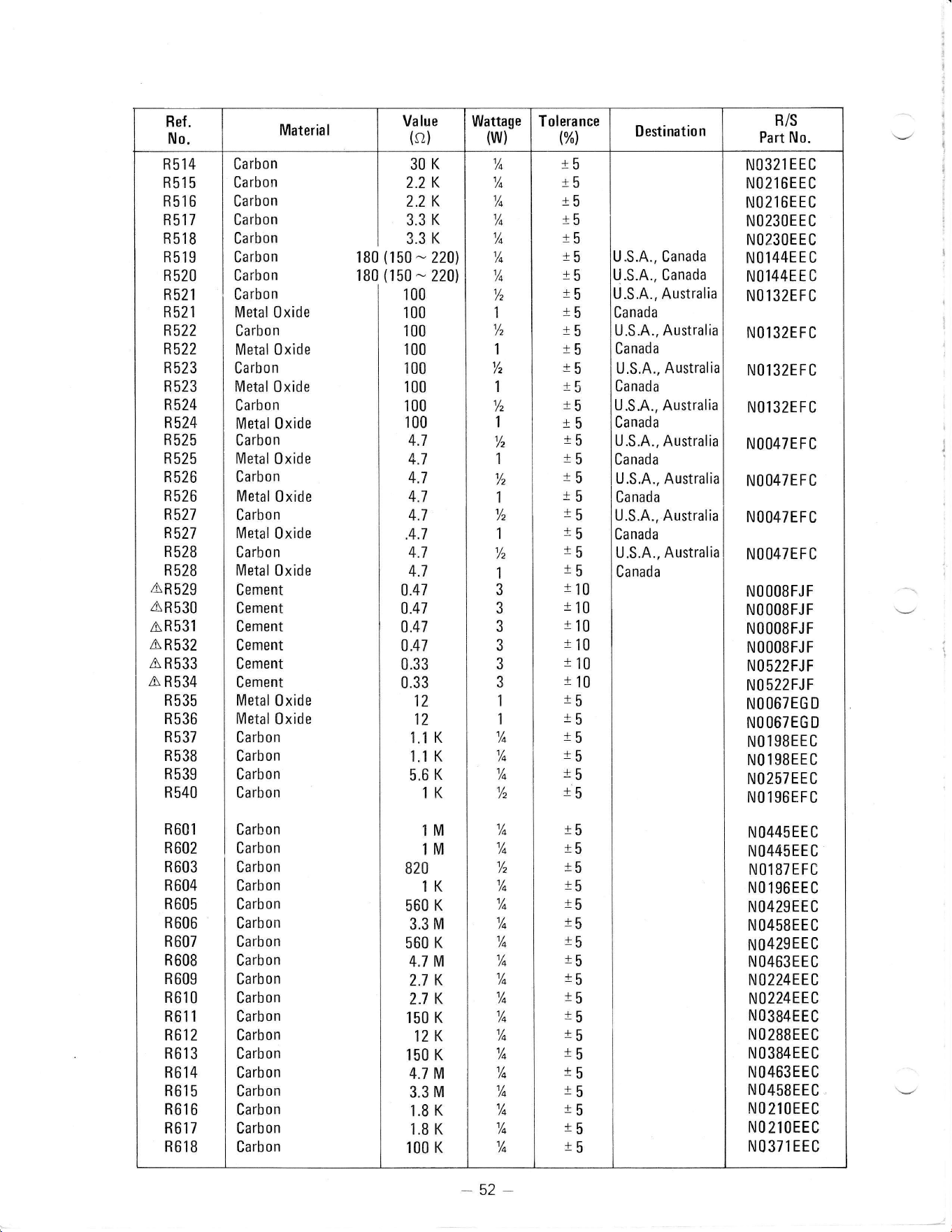
Bef
.
No.
Material
Value
(o)
Wattage
M}
Tolerance
MI
Destination
R/S
Part
No.
R514
R515
R516
R517
R
518
R519
R520
R
521
R52 1
R522
R522
R523
R
523
R524
R
524
R525
R525
R526
8526
R527
R527
R528
R528
4R529
AR530
AR531
A
R532
A
R533
A
R534
R535
R536
R537
R538
R539
R540
R601
R602
R603
R604
R605
R606
R607
B60B
R609
R61
0
R61 1
R 612
R
613
R614
R61 5
861 6
R
617
R6IB
Carbon
Carb
on
Carbon
Carbon
Carbon
Carbon
Carbon
Carbon
Metal 0xide
Carbon
Metal 0xide
Carbon
Metal
0xide
Carbon
Metal
0xide
Carbon
Metal 0 xide
Carbon
Metal
0xide
Carbon
Metal 0xide
Carbon
Metal
0xide
Cement
Cement
Cement
Cement
Cement
Cement
Metal
0xide
Metal
0xide
Carbon
Carbon
Carbon
Carbon
Carbon
Carbon
Carbon
Carbon
Carb
o n
Carb o n
Carbon
Carbon
Carbon
Carbon
Carbon
Carbon
Carbon
Carbon
Carbon
Carbon
Carbon
Carbon
180
180
30K
2.2
K
2.2
K
3.3
K
3.3
K
(150
-
220l
(150
-
220)
100
100
100
100
100
100
100
100
4.7
4.7
4.7
4.1
4.7
.4.7
4.7
4.1
0.47
0.41
0.47
0.47
0.33
0.33
12
12
1.1
K
1.1 K
5.6
K
1K
1M
1M
820
1K
560
K
3.3
M
560
K
4.7 M
2.1
K
2.7
K
150 K
12K
150 K
4.7 Nl
3.3
M
1.8
K
1.8 K
100 K
%
1/
%
lo
/4
To
v"
1
12
1
v,
1
,/z
1
72
1
%
1
v,
1
1/
/2
1
3
3
3
3
3
3
1
1
'/4
%
lo
1/
/2
%
To
1/
/2
lo
%
,/o
'/q
%
/4
lo
/4
/4
/4
lo
1/o
To
1t
l4
T"
r5
t5
t5
t5
t5
t5
t5
15
r5
r5
15
r5
l5
r5
t5
15
r5
t5
15
t5
15
15
15
r10
r
10
r
10
t10
r10
j
10
t5
15
t5
15
15
15
t5
t5
r5
15
t5
15
r5
15
r5
t5
15
15
15
r5
15
15
15
15
U.S.A.,
Canada
U.S.A., Canada
U.S.A.,
Australia
Canada
U.S.A.,
Australia
Canada
U.S.A.,
Australia
Canada
U.S.A., Australia
Canada
U.S.A., Australia
Canada
U.S.A., Australia
Canada
U.S.A.,
Australia
Canada
U.S.A.,
Australia
Canada
N0321
EEC
N02
1 6EEC
N02
1
6E
EC
N0230E
EC
N(]23()EE
C
N0144EEC
N0144E
E C
N0132EFC
N0132EFC
N0r
32E
F C
N0r
32E
F C
N0047EFC
N0047EFC
N0047EFC
N()O47
E
F C
N(]t}()BFJ F
NO()OSFJF
N()()()S FJ F
N
()O()S
FJ F
NO
522FJ
F
N() 522FJ
F
N()06TEG
D
N(}06TEG D
N0
1
98EE C
N0
I
98EEC
N0 257EEC
N0 r
96E
FC
N0445EEC
N()445EEC
N()IBTEFC
N0196EEC
N0429
EE
C
N0458EEC
N0429EEC
N(]463EEC
N()224EEC
N
()
224EE C
N
()
384EE
C
N0
288E
E
C
N0384EEC
N0463EEC
N
(]458EE
C
N0
21 0EE C
N0
2
1
0EEC
N0371EEC
-52-
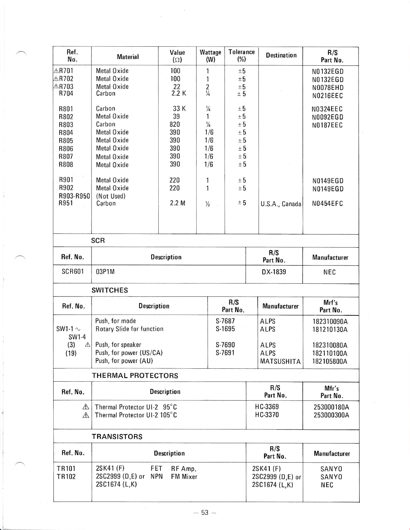
Ref .
No.
Material
Value
(o)
Wattage
(w)
Tolera
nce
(%l
Destination
B/S
Part
No.
AR701
AR702
AR703
R704
R80 1
RB02
HB()3
R804
RBOS
R806
RB()T
R808
R90
1
R902
R903-R950
R95 1
Metal 0xide
Metal
0xide
Metal
0xide
Carbon
Carb
on
Metal 0xide
Carbon
Metal 0xide
Metal 0xide
Metal
0xide
Metal
0xide
Metal
0xide
Metal
0xide
Metal
0xide
(Not
Used)
Carbon
100
100
22
2.2 K
33K
39
820
390
390
390
390
390
220
220
2.2M
1
1
2
Yq
To
1
/4
1t6
116
116
116
1t6
1
1
/2
t5
t5
t5
t5
t5
t5
t5
t5
t5
t5
t5
t5
t5
t5
r5
U.S.A.,
Canada
NOl32EGD
N() 132EGD
NOOTSEH D
N021
6EEC
NO 324E
E
C
N()O92EG
D
N0187EEC
N()I49EGD
N()149EG
D
N0454EFC
scR
Bef.
No.
Description
R/S
Part
No.
Manufacturer
sc
R601
O3P1
M
DX-1839
NEC
SWITCHES
Bef. No.
Description
R/S
Part
No.
Manufacturer
Mrf's
Part
No.
swl-1
.v
SWl-4
(3)
a
(1e)
Push,
for
mode
Rotary
Slide
for function
Push, for
speaker
Push, for
power
(US/CA)
Push, for
power
(AU)
s-7687
s-1 695
s.76s0
s-7691
ALPS
ALPS
ALPS
ALPS
MATSUSHITA
1
823
1
0090A
181210130A
1
823
1
0080A
1821 10100A
1
82 1
058004
THERMAL PROTECTORS
Hef.
No.
Description
R/S
Part
No.
Mfr's
Part
No.
,/N
A
Thermal
Protector
UI-2
95"C
Thermal
Protector
Ul-2
105'C
H
C-3369
H
C-3370
253000
1
80A
2530003004
TRANSISTORS
Ref. No.
Description
Ris
Part
No.
Manufacturer
TR 101
TR 102
2SK41
(F)
FET
RF
Amp.
25C2999
(D,E)
or NPN
FM Mixer
2SC1674
(L,K)
25K41
(F)
2SC29gg
(D,E)
or
2SC1
674
(L,K)
SANYO
SANYO
NEC
1
I
t
53-
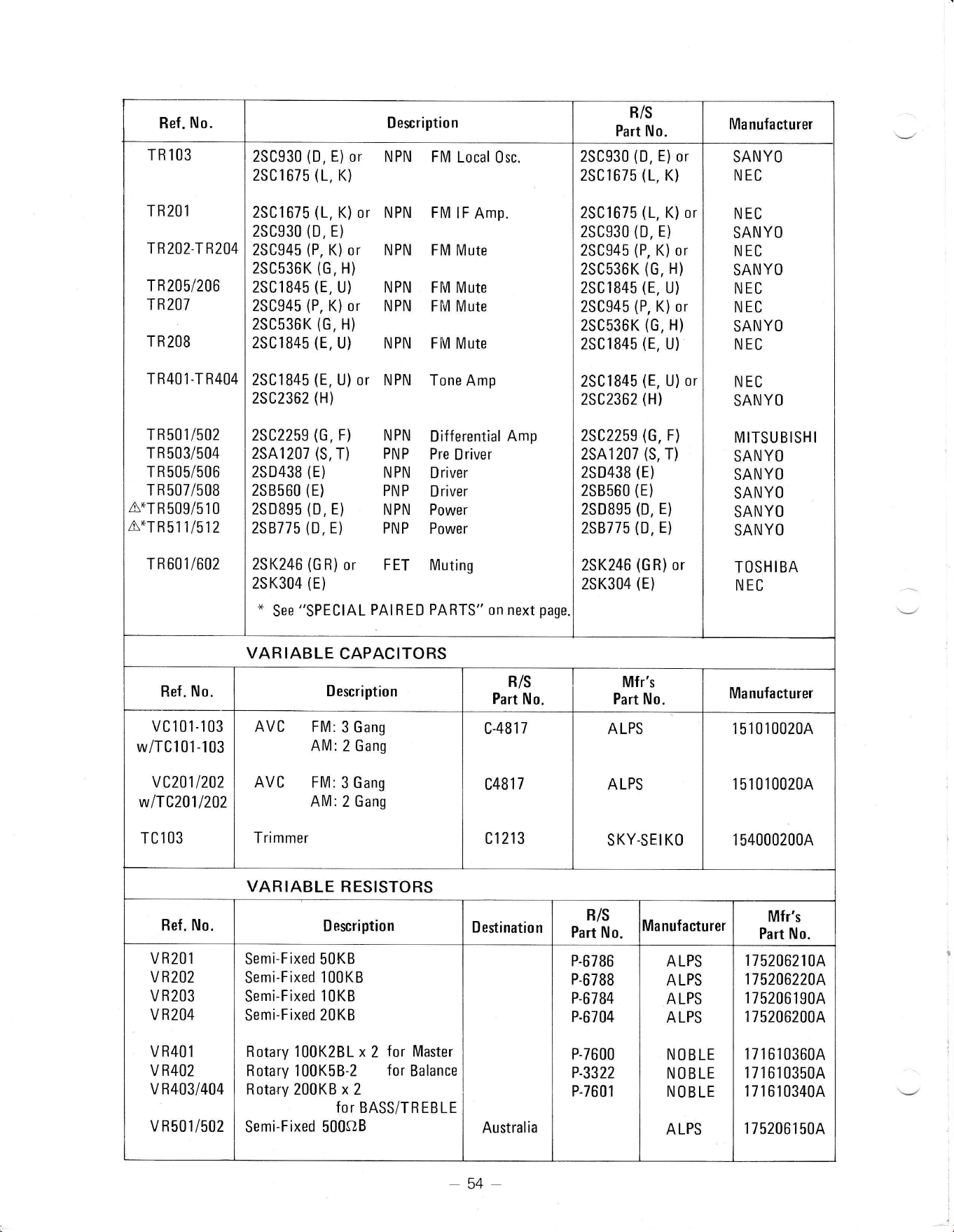
Bef.
No. Description
R/S
Part No.
Manufacturer
TR103
TB201
TR202-TR204
T
R
205/206
TRZOI
TR2()B
TR401.T8404
TR501/502
T R
503/504
T
R505/506
T R507/508
a-T
R
509/510
a-T
R
51
1/512
TR60ri602
2SC930
(D,
E) or NPN
25C1
675
(1,
K)
2SC1
675
(1,
K) or NPN
25C930
(0,
E)
2SC945
(P,
K) or NPN
2SC536K
(G,
H)
zSC1B45
(E,
U) NPN
2SC945
(P,
K) or NPN
25C536K
(G,
H)
25C1845
(E,
U) NPN
25C1845
(E,
U) or
NPN
25C2362
(H)
2SC2259
(G,
F)
NPN
2SA1207
(S,
T)
PNP
2SD438
(E)
NPN
258560
(E)
PNP
2SDB95
(D,
E)
NPN
258775
(D,
E)
PNP
25K246
(GR)
or FET
25K304
(E)
FM Local
0sc.
FM
lF Amp.
FM
Mute
FM
Mute
Fl'/l
Mute
FM Mute
Tone
Amp
Differential
Amp
Pre D river
D
river
D
river
Power
Power
Muting
See
"SPECIAL
PAIRED
PARTS" on next
page.
2SC930
(D,
E)
or
25C1675
(1,
K)
2SC1675
(1,
K) or
25C930
(D,
E)
25C945
(P,
K)
or
2SC536K
(G,
H)
25C1845
(E,
U)
25C945
(P,
K) or
2SC536K
(G,
H)
25C1845
(E,
U)
25ClB45
(E,
U)
or
2SC2362
(H)
2SC2259
(G,
F)
2SA1207
(S,
T)
2SD43B
(E)
258560
(E)
2S0895
(D,
E)
258775
(D,
E)
2SK246
(GR)
or
2SK304
(E)
SANYO
NEC
NEC
SANYO
NEC
SANYO
NEC
NEC
SANYO
NEC
NEC
SANYO
M
ITSU BISH
I
SANYO
SANYO
SANYO
SANYO
SANYO
TOSH
I
BA
NEC
VARIABLE
CAPACITORS
Ref.
No.
Description
R/S
Part No.
Mfr's
Part
No.
Manufacturer
vc
101-103
wiTC101-103
vc2011202
wlTC2011202
TC103
AVC FM:
3
Gang
AM:
2
Gang
AVC FM:3
Gang
AM: 2 Gang
Trimmer
c-4817
c4817
c1213
ALPS
ALPS
SKY.SEIKO
151010020A
151010020A
1
54000200A
VARIABLE RESISTORS
Ref. No.
Description
Destination
B/S
Part
No.
Manufacturer
Mfr's
Part No.
VR201
vR202
VR2O3
VR204
VB4(]1
VR402
v R403/404
vR501/502
Semi-Fixed 50KB
Semi-Fixed
100K8
Semi-Fixed
10KB
Semi-Fixed
20KB
Rotary 100K2BL x2
Ior Master
Rotary 100K58-2
for
Balance
Rotary 200KB
x
2
for
BASS/TR
EB LE
Semi-Fixed 500srB
Australia
P-6786
P-6788
P-6784
P-6704
P-7600
P-3322
P-7601
ALPS
ALPS
ALPS
ALPS
NOBLE
NOBLE
NOBLE
ALPS
175206210A
175206220A
1
75206190A
1 75206200A
1716103604
171610350A
171610340A
1 752061 50A
54-
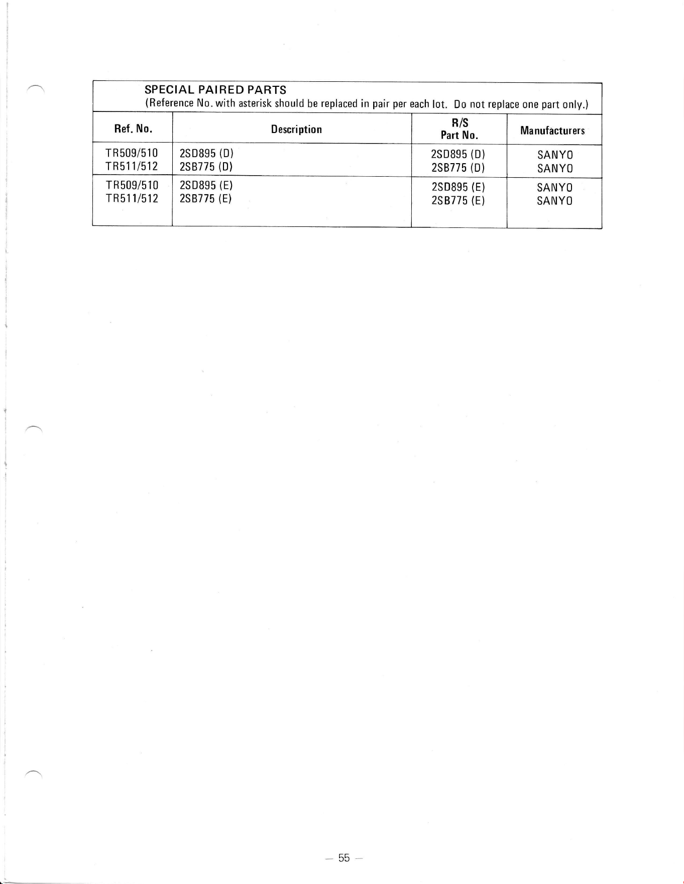
SPECIAL
PAIRED PARTS
(Reference
No. with
asterisk
should
be
replaced in
pair per
each lot.
Do
not replace
one
part
only.)
Ref.
No.
Description
nis
Part
No.
Manufacturers
TR509/510
TR511/512
250895
(D)
258775
(D)
25D8s5
(D)
258775
(D)
SANYO
SANYO
TR
509/510
TRs111512
250895
(E)
258775
(E)
250895
(E)
258775
(E)
SANYO
SANYO
-55-

Hef. No.
Description
R/S
Part No.
Mfr's
Part No.
1
2
3
4
5
6
7
I
I
10
11
12
13
14
15
16
17
1B
a1g
a22
a23
24
a25
26
20
A"21
27
28
29
30
31
32
33
34
35
36
37
38
39
Terminal Nip,
Speaker
Terminal
Screw, Antenna
Switch,
Push,
Speaker
Jack,
6.3,
Headphone
Clip, Fuse
Pointer
Pointer
Base
with
Sheet
Pu
lley,
G uide
Shaft
Ass'y,
Tuning
Back
Board,
Dial
Scale,
D ial
Blind, Lamp Dial
Side,
Dial
Spring
Bar,
Side
Dial
Holder,
Lamp
Lamp,
Tubular, Fuse
Type 12.5V/0.15A
(U.S.A.)
Lamp,
Tubular, Fuse
Type 12Vl0.15A
(Canada/Australia)
Pulley,
Dial
P.
C. B.
Ass'y,Speaker
Switch
Switch,
Push, Power
(U.S.A./Canada)
Switch,
Push,
Power
(Australia)
Shaft, Joint,
Switch
Power
Transformer,
Power
(U.S.A.)
Transf ormer,
Power
(
Canada)
Transf ormer,
Power
(Australia)
Protector,
Thermal
Protector,
Thermal
Holder,
Fuse
(U.S.A.)
Holder,
Fuse
(Canada)
Holder,
Fuse
(Australia)
AC 0utlet
(U.S.A./Australia)
AC
0utlet
(Canada)
Panel,
Back
(U.S.A.)
Panel,
Back
(Canada)
Panel,
Back
(Australia)
Antenna,
Bar
Cover,
Antenna
Bar
Holder,
Antenna
Bar
Screw,
Ground
Holder,
Cabinet/Board, Back
Panel
Ass'y,
Front,
Non-repairable
Panel,
Front,
Window, Dial
Blind,
Aluminum
Spacer
Knob,
Push,
Square
Shaft, Joint,
Knob
Push
Spring, Coil, Knob Push
Knob,
Tuning
Knob,
Volume
Knob,
Selector/Tone
Knob, Power
J-5108
s-7690
J-1423
F-1
208
D-0489
D-3318
D-5600
D-5601
H
C-3366
D-5602
H
C-3367
F-1
209
D-0574
x-9985
s-7691
H
C-3368
TA-1106
H
C-3369
H
C-3370
F-1
206
w-3026
z-7623
cA-0758
H C-3372
A-4484
HC-1574
z-7622
K-5859
K-5860
K-586r
K-5862
192310040A
1
9221 0070A
1
8231 0080A
191010090A
1 97303080A
43521
0050A
4351
1 0020A
433
1
00420A
431010010A
41 651
01 00A
717010180A
85 1 21
0970A
713410060A
43451
01 50A
1
97
1
001 20A
24301 0020A
243001 320A
433002390A
u-23265
1821 10100A
1
821 05800A
432008680A
10101 114SA
10101115SA
10101
1 165A
253000 1
B0A
253000300A
1970001
10A
or
197000200A
1
970001
30A
1970001
50A
1 9601
0020A
1 960
1 0040A
7070 1
0420A
7070
1 0430A
70701
0440A
111010080A
60231 00308
41 3003s00A
HMWOAOO2SN
4t
30087 1
0A
M-00375
701
01
01 30A
7136100804
851 21
0980A
852002780A
65951 0430A
43201 0070A
4341 10190A
65251 0320A
65251
0330A
652510310A
6550 1 0080A
EXPLODED VIEW PARTS
LIST
56-
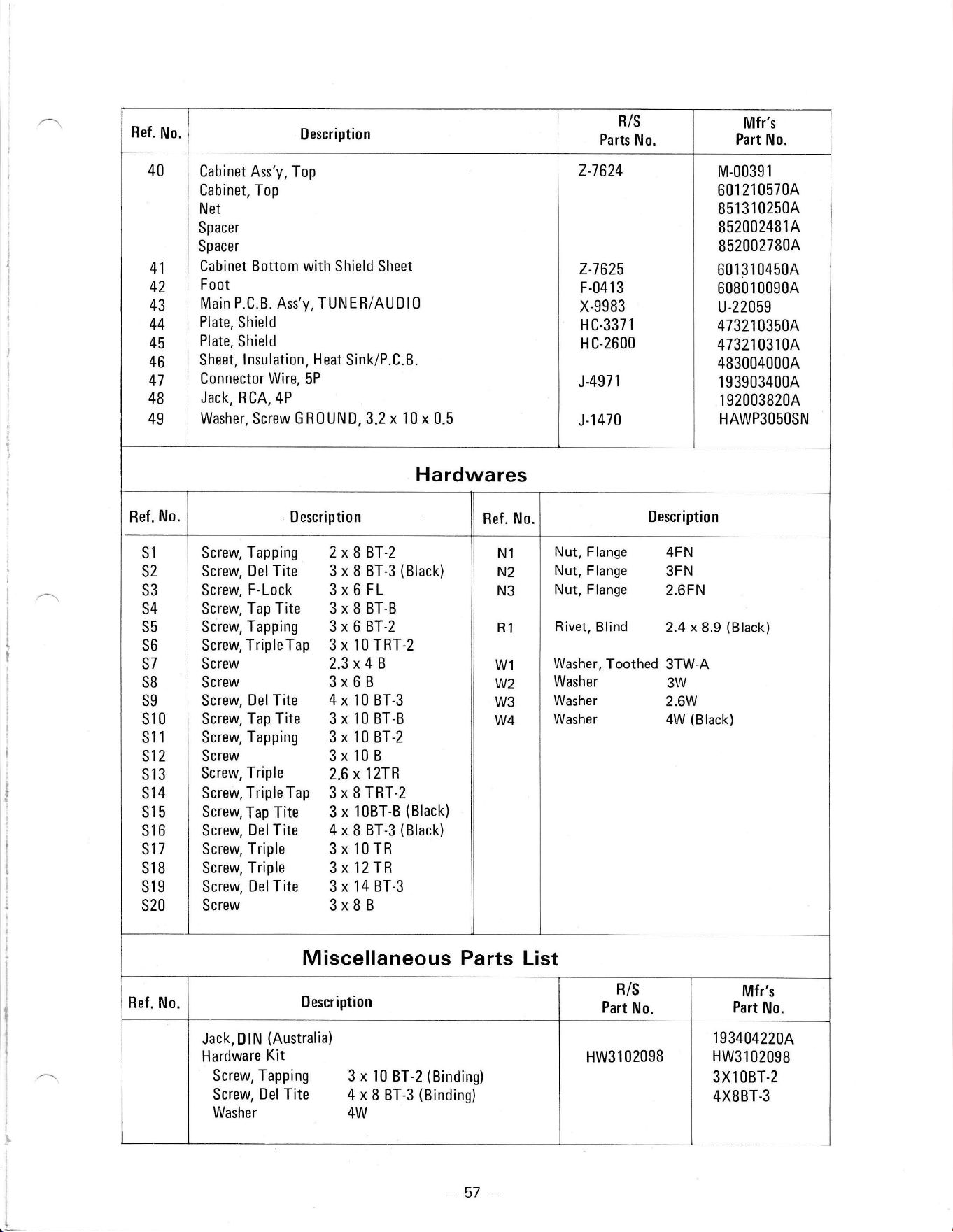
Bef.
No.
Descriptio
n
B/S
Parts
No.
Mfr's
Part No.
40
41
42
43
44
45
46
47
4B
49
Cabinet Ass'y,
Top
Cabinet, Top
Net
Spacer
Sp
acer
Cabinet Bottom
with
Shield Sheet
Foot
Main
P.C.B.
Ass'y, TUNER/AUDl0
Plate,
shield
Plate,
Shield
Sheet,
lnsulation,
Heat
Sink/P.C.B.
Connector
Wire,
5P
Jack,
R CA,
4P
Washer, Screw
G R0UND,
3.2
x 10 x
0.5
z-1624
z-7625
F-0413
x-9983
H
C-3371
H C-2600
J-4971
J-1 470
M-00391
601
210570A
85r 3
1 0250A
85200248
1 A
852002780A
6013104504
6080 1 0090A
u-22059
4732
1 0350A
47321 03 1 0A
483004000A
1 93903400A
1 92003820A
HAWP3OSOSN
Hardwares
Ref.
No.
D
escrip
ti o n
Ref.
No.
Description
S1
S2
S3
S4
S5
S6
S7
S8
S9
s10
s11
s12
s13
s14
s15
s16
s17
S1B
s19
s20
Screw,
Tapping
Screw,
DelTite
Screw,
F-Lock
Screw,
Tap Tite
Screw,
Tapping
Screw,
Triple Tap
Screw
Screw
Screw,
DelTite
Screw,
Tap Tite
Screw,
Tapping
Screw
Screw,
Triple
Screw,
Triple Tap
Screw,
Tap
Tite
Screw,
DelTite
Screw,
Triple
Screw, Triple
Screw,
DelTite
Screw
2xBBT-2
3x8BT-3(Black)
3
x
6
FL
3xBBT-B
3xGBT-2
3 x'10 TRT-2
2.3x48
3xGB
4
x 10 BT-3
3
x 10 BT-B
3
x 10
BT-2
3 x 10 B
2.6
x 12TR
3 x
B
TRT-2
3
x
10BT-B
(Black)
4xBBT-3(Black)
3 x 10 TR
3x 12TR
3
x 14 BT-3
3xBB
N1
N2
N3
R1
W,I
w2
W3
W4
Nut, Flange
4FN
Nut, Flange
3FN
Nut, Flange
2.6FN
Rivet,
Blind
2.4 x
8.9
(Black)
Washer,
Toothed
3TW-A
Washer
3W
Washer
2.6W
Washer
4W
(Black)
Miscellaneous
Parts List
Ref. No.
Description
B/S
Part
No.
Mfr's
Part
No.
Jack,
D
lN
(Australia)
Hardware
Kit
Screw, Tapping
3
x 10
BT-2
(Binding)
Screw,
Del Tite
4
x
8 BT-3
(Binding)
Washer
4W
HW3102098
193404220A
HW31020gB
3X10BT-2
4XBBT-3
-51
-
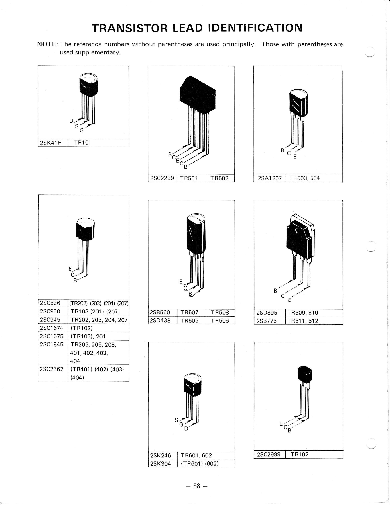
TRANSISTOR LEAD
IDENTIFICATION
NOTE: The
reference
numbers
without
parentheses
are used
principally.
Those with
parentheses
are
used supplementary.
s-G
25C2259
I
TR501
TR502
2S8560 TR5O7 TR5O8
2SD438 TR5O5
TR506
25K246
TR601, 602
25K304
(TR601) (602)
2SA12O7
I
TR503,504
2SD895 TR509, 51
0
258775
TR51
1. 5i 2
B
TR1
02
2SC536
(TR202)
(n3l
lrul
(n7
2SC930
TR103
(2011 (2071
2SC945 rR202,203,204,207
25C1674
(TR102)
25C1
675
(TR103),
201
2SC1 845 TR205,2A6,208,
401,402,403,
404
25C2362
(TR401)
(402) (40s)
(4041
-58-
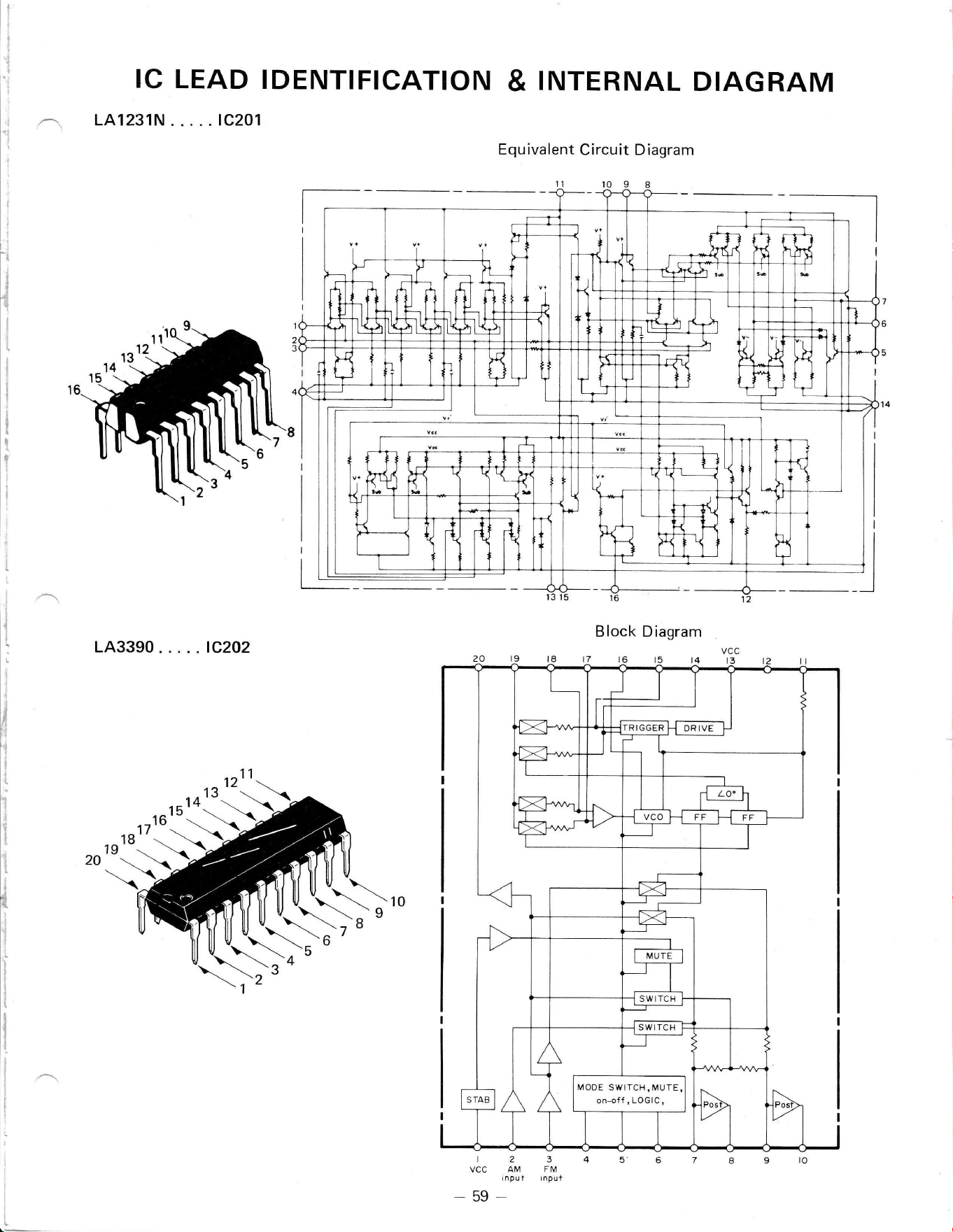
1
'j
:
i
--\
'i
t,
t
l
ll
IC LEAD
IDENTIFICATION
LA1231N 1C201
&
INTERNAL
DIAGRAM
Equivalent
Circuit D iagram
1A3390
.
....1C202
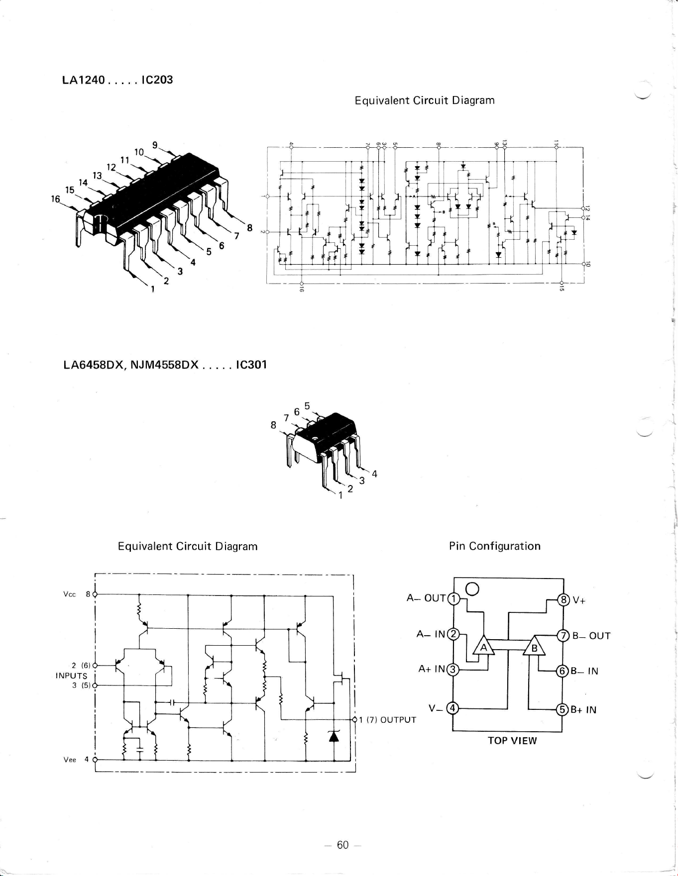
LA1240 tC203
LA6458DX,
NJM4558DX
. .
. .
.
1C301
Equivalent Circuit Diagram
Equivalent Ci
rcuit Diagram
Pin
Configuration
A_
OUT
A_ IN
A+l
V+
B_
OUT
B_
IN
B+
lN
I
I
TOP
VIEW
-60
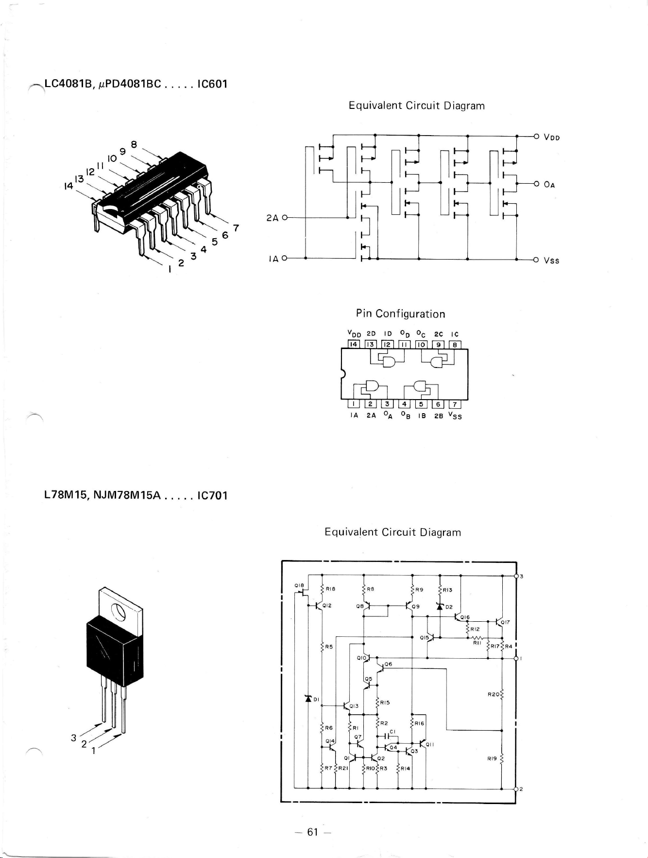
Voo
Equivalent
Circuit Diagram
Equivalent
Circuit
Diagram
3-o^
2A
IA
L78M15,
NJM78M15A.
. . . .
1C701
Ol2
OA
-61
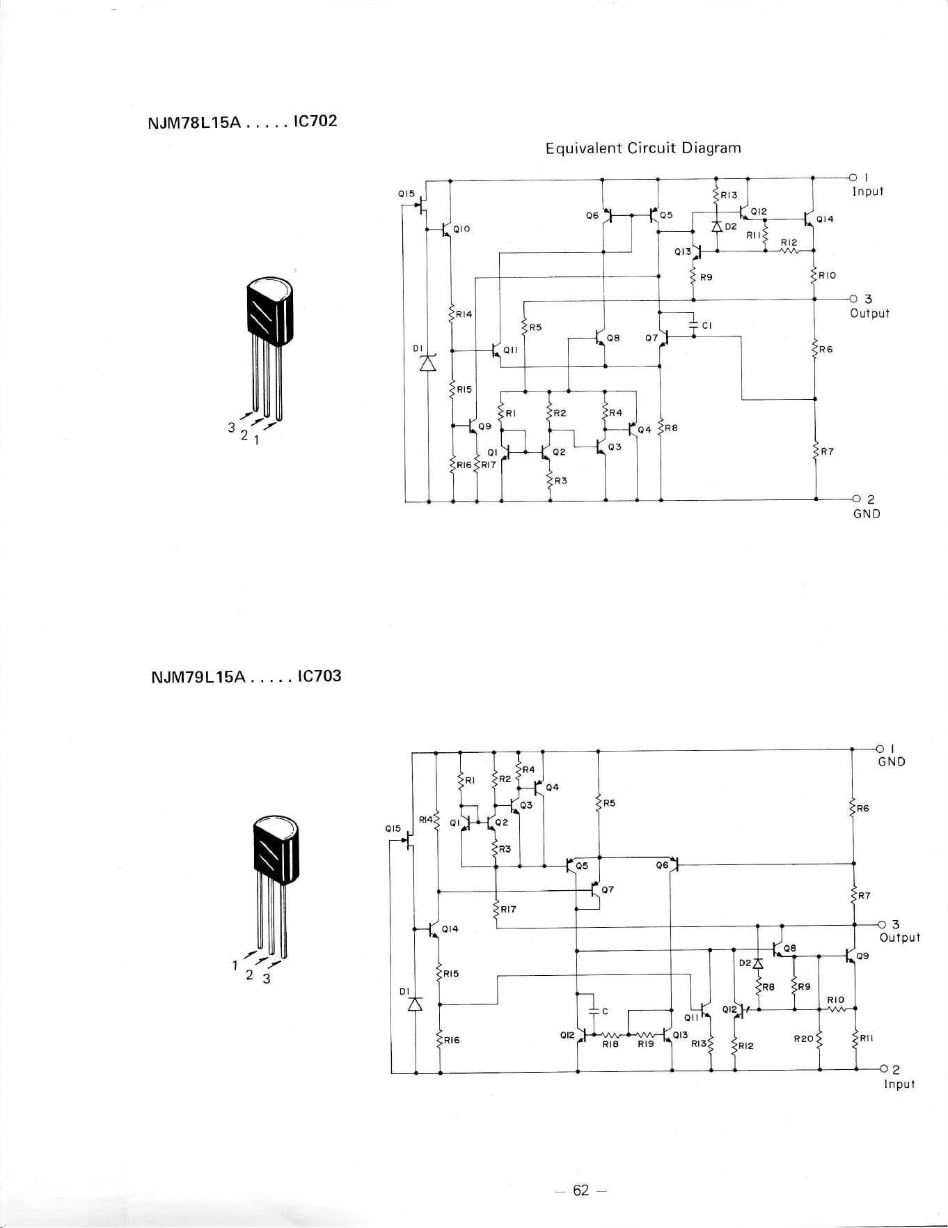
NJM78L15A.....1c702
NJM79115A.....1c703
Equivalent
Circuit
Diagram
Oul
put
ffi
2g
3
Ou
t
put
62-
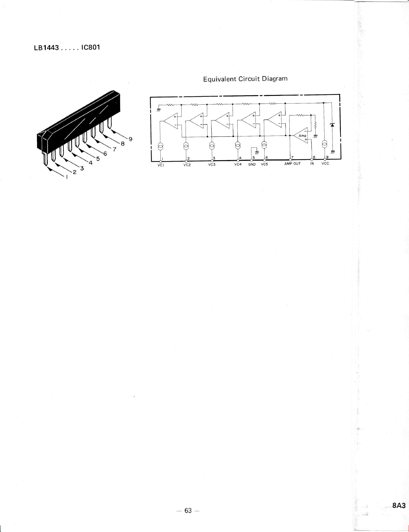
181443.....1C801
Equivalent
Circuit
D iagram
63
843
SCHEMATIC
DIAGR
_c205
o.or
cro2
30P
,/ ln tol
Rlog
/'
25C950(O.E)
330
/or
zSC 1675(L.X)RlOa
22R
cil2
IoPNPo)
TRrO2
2SC2999(D.E)
or 2SCl674(L.K)
R lo4
too
c26 I
.o22
TR20t
2SC950(D.E)
or
2SCl675(L.K)
R205
too
!
c202
a o47
"'
R2t2 56K
R204
33O
O2Ol
ITTBN,
or
0S442X
toK
TRtOt
2SX4t(F)
cto3
IP
(NPO)
_lL
l202
I
B'.3i
rlf
I oo
|
-r*
I lzot
II
ft.toI
lrepl
bPd
olo I
lTT73N or
os422X
Ril4
0r03
cI9
.o47
7f
7l T6
. I I
=tN
t205
c252
2.2tH
36OP
tc202
LA-3390
2
t9
R234
20K
c?62
.o47
3
t8 t7
R 254
390
e
2i
RZ
68
RZ
e8
c234
a
a?oP
I
I
c233
820P
63
N
r
RS9
56K
R233
20K
502
2sc2259lc.F) tz
R262 rok
xx
TAPE IN/OUT
OIN JACK
(AUSTRALIAN
MODELS
ONLY)
J-
raPE
our
I
|
,or.
,,
I
I
AUX
I
L
"roro
I
PHoNo
I
I
aux
3
,i
I
TAPE lN
I
L
roo. n,,t
R442
680
TUNER
/ AUDIO P C. B.
tc20t
LA-t23tN
o,o2
rctzz fct23
:Arr-zorT
O.Ol
'fO.O?"
rcK I rTT4tO 270K
"z
snlczte
l"* P
*--E!
P*
czii
azzt |
''
I f12(
o47 lK
f r, I i(,.*.T
c23a
R22s s.rK c2ji
*
/tiakB-lloooP
aR40r,
-
TR404
2sclA45
(E.U)
or
zsc2362(H)
x4
R3t7 4701t/2)
T r*TF< Cdd
R5o7
t
efra
2.2K
R437 or
2sK3o4(E)
R5o3 cst
tK
..-,. ....
tK
z.Ua
\Ti
slqw
I
qFr-l
,L
I
c
c3o6
R446
47t16
4.7K
rR4o4
I
c426
oz2 L
on.-L-J
rql
td} f
tMd
veon it5*
47
(1)
t2l
(3)
l4l
(s)
(6)
SWl-1
-
SWI.4 INDICATE FUNCTION
SELECTOR
SW
(AM,
FM, FM-MUTE,
PHONO,
AUX.TY)
ALL RESISTANCE
VALUES ARE INDICATED
lN
"OHM"
(K
- 103
OHM,
M
= 106
OHM)
ALL
CAPACITANCE VALUES ARE INDICATED
lN "1tF"
(P
= 10-6
pF)
*
VALUES
ARE USED FOR
CANADIAN MODELS
ONLY.
+ +
VALUES
MAY VABY
FROM
UNIT
TO UNIT FOB
BEST
PERFORMANCE.
FOR AUSTRALIAN
MODELS
VR5OlandVR5O2(50OOB)
ARE
USED lN
PLACE
OF R519andR52O
CAUTI(
Before
r
measurt
circu
it-
NOTES:
-64-
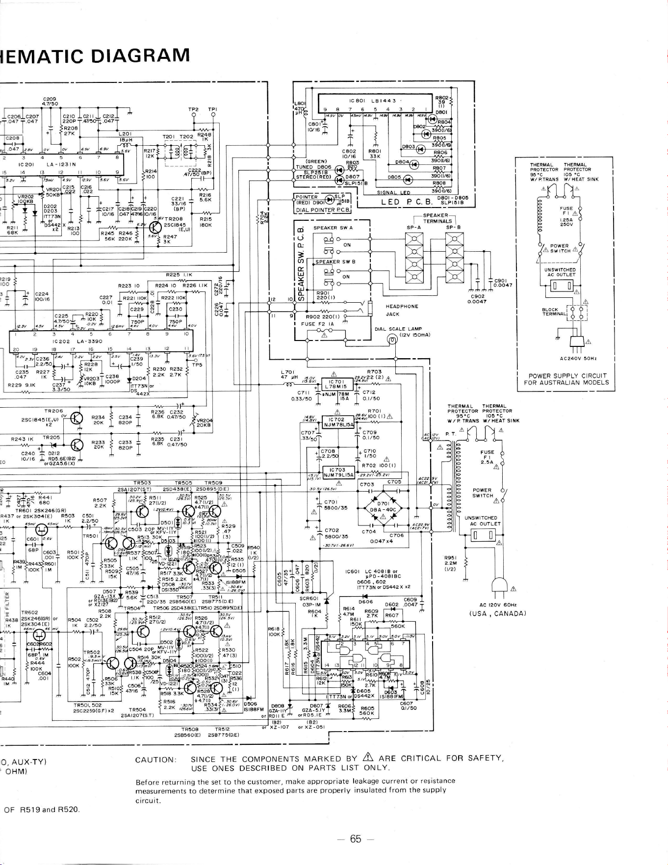
IEMATIC
DIAGRAM
TP2 TPI
345
lc20t LA-t23tN
t4
c235 R227
o47 t(
R229 9.lK
C2
[-*;r*u-o;--_l
I
PRoTECTR
PRoTEcToR
i
r S'C lO5
"C
I w/PTRANS W/HEAT stNx I
.:t
Fi5,,l
i
LEo
PC.B.
-._-
lI
IG
!
FUSE F2 IA
-
-]
I
E19
loo
rf
,T
SPEAKER SW A
R902 220(r)
HEADPHONE
JACK
OIAL SCALE LAMP
(l2v
l5oma)
tL
L__
L70t
47
DH
A
R703
212)
A
! ,o*.* ,rr".., .,*.r,t I
l_111usrnarraru
uoo11_l
TR2O6
2SC rA45
(E,U)
t2
R243 rK
A
PT.
R233
20K
c233
a20P
R235
C23r
o.ex
o.4?/5O
2)
(82)
-l07 or
XZ -05l
CAUTION:
SINCE
THE COMPONENTS
MARKED
EY A ANE CRITICAL
FOR SAFETY,
USE ONES
DESCRIBED
ON
PARTS LIST ONLY.
Before
returning
the set to the
customer,
make appropriate
leakage current or resistance
measurements to determine
that
exposed
parts
are
properly
insulated
from the
supply
ci rcu
it.
I
,
6
a
I
h
*
=
c24O
^
O"t?
rolr6 I RD5.6E(Ba
"'orczA5.6(x)
O,
AUX.TY)
'oHM)
OF R519
and
R520.
rcaor
Lar443
q6765432
C22l
f
5.6K
33/t6 1
R2?4 tO R??6
t.lK
1c202 LA-3390
R250 R232
?.2K 2.7K
'n*v'
rao-&'1Y)loo
t
t
t
a
cTor I f
5aoo/35
K*
t\
L-,
C7O2
c7O4
O.O47
x4
lc6ol Lc
4oalB
or
rPD
-4Og
I BC
0606
,
5O2
ITT73N
6 OS€2x
x2
SlHiii*"1
+J22ol35
2sBs6o(E)
zsB775(o
E)
T l* lel l-]!+r"#
J I
Jtl
l'ilrt.m+
TR50r,502
2sc2259(G.F)
t2
TR5o4
2sar207(sT)
A
I
A
R530
47(3)
_SPEAKER_
I
renurus
I
SP.A SP.8
c902
o.oo47
E
A
l\
sw rrcs
A
Ll---------J
UNSWITCHED
65-
!
1
lt
1
,i
'
i
<r
t_
f
i
I
I
i
!
RADIO
SHACK,
A DIVISION
OF
TANDY CORPORATION
U.S.A.:
FORT WORTH,
TEXAS
76102
CANADA:
BARRIE, ONTARIO
L4M
4W5
AUSTRALIA
TANDY
CORPORATION
BELGIUM
U.K
91
KURRAJONG AVENUE
MOUNT DRUITT, N.S.W. 2770
PARC INDUSTRIEL
DE NANINNE
5140 NANINNE
BILSTON
ROAD WEDNESBURY
WEST
MIDLANDS
WS1O 7JN
,l
1
8A3
Printed
in
Korea
8111102504
.-*
!