– 1 –
CD-BK250W/CD-BK2600W/CD-BK270W
No. S5136CDBK250W
CONTENTS
Page
SAFETY PRECAUTION FOR SERVICE MANUAL ........................................................................................................... 2
VOLTAGE SELECTION ..................................................................................................................................................... 2
AC POWER SUPPLY CORD AND AC PLUG ADAPTOR ................................................................................................. 2
SPECIFICATIONS ............................................................................................................................................................. 3
NAMES OF PARTS ........................................................................................................................................................... 4
OPERATION MANUAL ...................................................................................................................................................... 7
DISASSEMBLY .................................................................................................................................................................. 9
REMOVING AND REINSTALLING THE MAIN PARTS ................................................................................................... 12
ADJUSTMENT ................................................................................................................................................................. 13
BLOCK DIAGRAM ........................................................................................................................................................... 17
SCHEMATIC DIAGRAM / WIRING SIDE OF P.W.BOARD ..............................................................................................20
VOLTAGE ........................................................................................................................................................................ 38
NOTES ON SCHEMATIC DIAGRAM .............................................................................................................................. 39
TYPES OF TRANSISTOR AND LED............................................................................................................................... 39
WAVEFORMS OF CD CIRCUIT ...................................................................................................................................... 40
TROUBLESHOOTING ..................................................................................................................................................... 41
FUNCTION TABLE OF IC................................................................................................................................................ 45
FL DISPLAY ..................................................................................................................................................................... 53
REPLACEMENT PARTS LIST/EXPLODED VIEW
• In the interests of user-safety the set should be restored to its
original condition and only parts identical to those specified be
used.
SERVICE MANUAL
This document has been published to be used
for after sales service only.
The contents are subject to change without notice.
SHARP CORPORATION
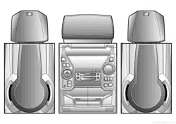
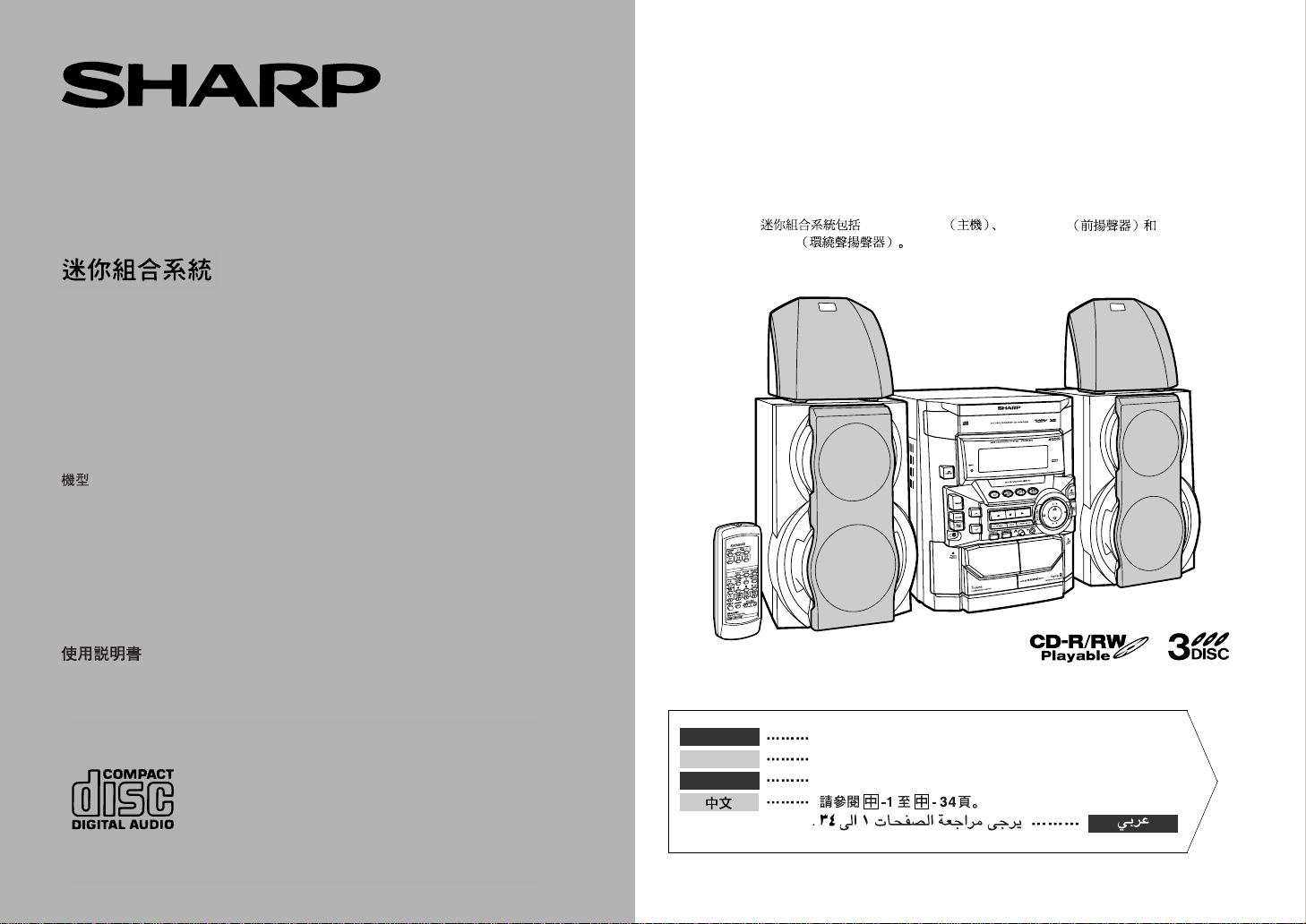
MINI COMPONENT SYSTEM
MODEL CD-BK250W
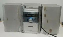
CD-BK250W Mini Component System consisting of
CD-BK250W (main unit) and CP-BK250 (speaker system).
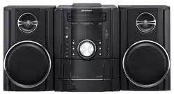
MINI COMPONENT SYSTEM
MODEL CD-BK2600W
CD-BK2600W Mini Component System consisting of
CD-BK2600W (main unit) and CP-BK2600 (speaker system).
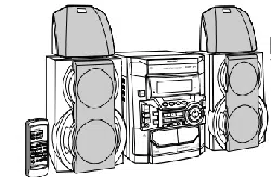
MINI COMPONENT SYSTEM
MODEL CD-BK270W
CD-BK270W Mini Component System consisting of
CD-BK270W (main unit), CP-BK270 (front speakers) and
GBOXS0070AWM1 (surround speakers).
Illustration: CD-BK250W/CD-BK2600W
Illustration: CD-BK270W
CD-BK250W/CD-BK2600W/CD-BK270W
– 2 –
QACCE0010AW00
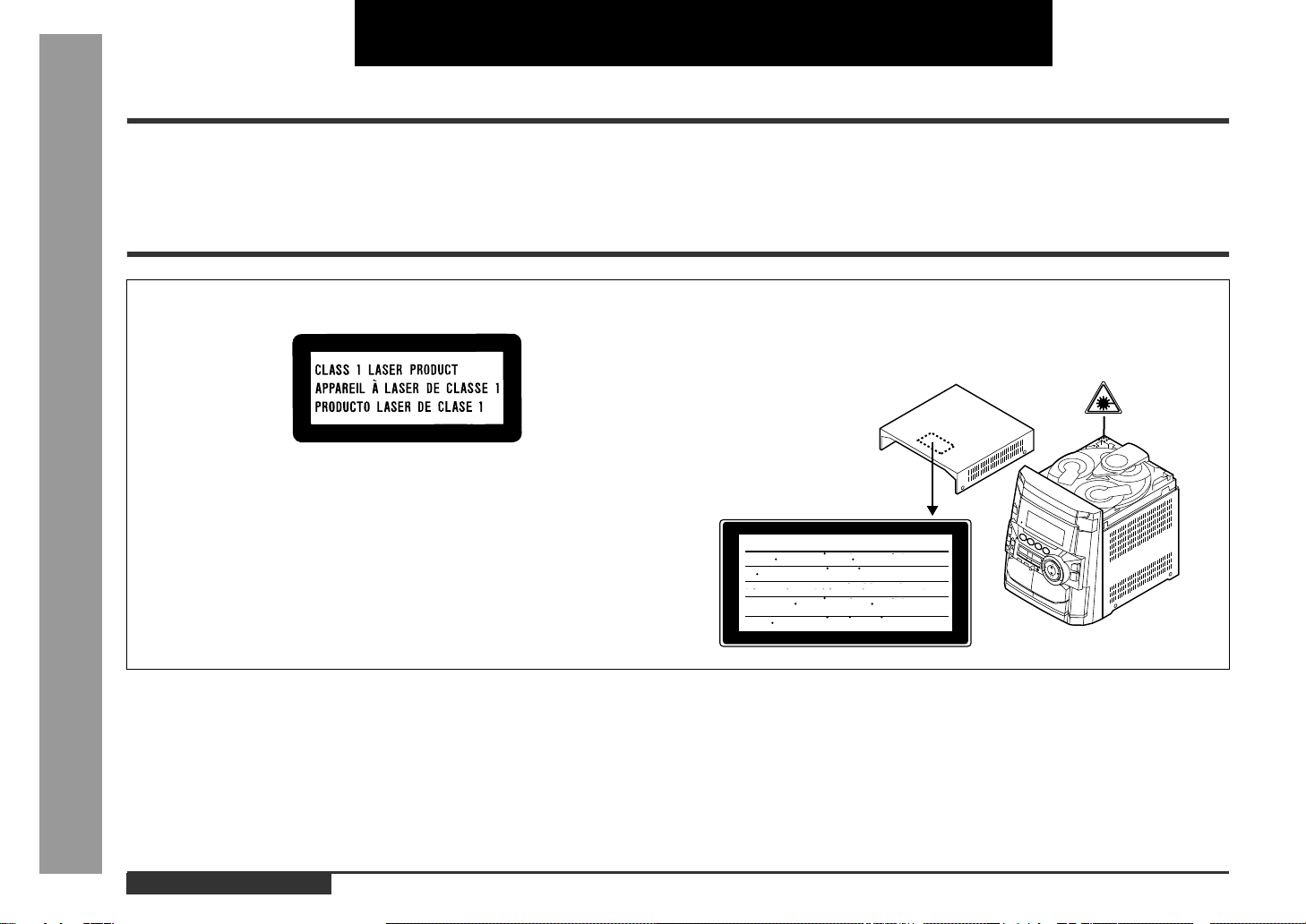
SAFETY PRECAUTION FOR SERVICE MANUAL
WARNINGS
THE AEL (ACCESSIBLE EMISSION LEVEL) OF THE LASER POWER OUTPUT IS LESS THAN CLASS 1 BUT THE LASER
COMPONENT IS CAPABLE OF EMITTING RADIATION EXCEEDING THE LIMIT FOR CLASS 1. THEREFORE IT IS
IMPORTANT THAT THE FOLLOWING PRECAUTIONS ARE OBSERVED DURING SERVICING TO PROTECT YOUR EYES
AGAINST EXPOSURE TO THE LASER BEAM.
1-WHEN THE CABINET IS REMOVED, THE POWER IS TURNED ON WITHOUT A COMPACT DISC IN POSITION AND THE
PICKUP IS ON THE OUTER EDGE THE LASER WILL LIGHT FOR SEVERAL SECONDS TO DETECT A DISC. DO NOT
LOOK INTO THE PICKUP LENS.
2-THE LASER POWER OUTPUT OF THE PICKUP UNIT AND REPLACEMENT SERVICE PARTS ARE ALL FACTORY
PRESET BEFORE SHIPMENT.
DO NOT ATTEMPT TO READJUST THE LASER PICKUP UNIT DURING REPLACEMENT OR SERVICING.
3-UNDER NO CIRCUMSTANCES STARE INTO THE PICKUP LENS AT ANY TIME.
4-CAUTION-USE OF CONTROLS OR ADJUSTMENTS, OR PERFORMANCE OF PROCEDURES OTHER THAN THOSE
SPECIFIED HEREIN MAY RESULT IN HAZARDOUS RADIATION EXPOSURE.
VOLTAGE SELECTION
Before operating the unit on mains, check the preset voltage. If the voltage is different from your local voltage, adjust the voltage
as follows.
Turn the selector with a screwdriver until the appropriate voltage number appears in the window (110 V, 127 V, 220 V or 230 V-240 V AC).
AC POWER SUPPLY CORD AND AC PLUG ADAPTOR
QACCA0003AW00
QACCL0005AW00
QACCJ0007AW00
QPLGA0003AWZZ QPLGA0004AWZZ
Laser Diode Properties
Material: GaAIAs
Wavelength: 780 nm
Emission Duration: continuous
Laser Output: max. 0.6 mW
CAUTION-INVISIBLE LASER RADIATION WHEN OPEN. DO NOT STARE INTO
BEAM OR VIEW DIRECTLY WITH OPTICAL INSTRUMENTS.
VARNING-OSYNLIG LASERSTRALNING NAR DENNA DEL AR OPPNAD. STIRRA
EJ IN I STRALEN OCH BETRAKTA EJ STRALEN MED OPTISKA INSTRUMENT.
ADVERSEL-USYNLIG LASERSTRALING VED ABNING. SE IKKE IND I
STRALEN-HELLER IKKE MED OPTISKE INSTRUMENTER.
VARO! AVATTAESSA OLET ALTTIINA NAKYMATON LASERSATEILYLLE.
ALA TUIJOTA SATEESEEN ALAKA KATSO SITA OPTISEN LAITTEEN LAPI.
VARNING-OSYNLIG LASERSTRALNING NAR DENNA DEL AR OPPNAD.
STIRRA EJ IN I STRALEN OCH BETRAKTA EJ STRALEN GENOM OPTISKT
INSTRUMENT.
ADVERSEL-USYNLIG LASERSTRALING NAR DEKSEL APNES. STIRR IKKE
INN I STRALEN ELLER SE DIREKTE MED OPTISKE INSTRUMENTER.
– 3 –
CD-BK250W/CD-BK2600W/CD-BK270W
FOR A COMPLETE DESCRIPTION OF THE OPERATION OF THIS UNIT, PLEASE REFER
TO THE OPERATION MANUAL.
Specifications for this model are subject to change without
prior notice.
SPECIFICATIONS
CP-BK250/CP-BK2600
CD-BK250W/CD-BK2600W
CD-BK270W
CP-BK270
GBOXS0070AWM1
General
Amplifier
CD player
Tuner
Cassette deck
Power source
AC 110/127/220/230 - 240 V, 50/60 Hz
Power consumption
130 W
Dimensions
Width: 270 mm (10-11/16")
Height: 330 mm (13")
Depth: 340 mm (13-3/8")
Weight
7.2 kg (15.7 lbs.)
Output power
MPO: 240 W (120 W + 120 W) (10 % T.H.D.)
RMS: 150 W (75 W + 75 W) (10 % T.H.D.)
RMS: 104 W (52 W + 52 W) (0.9 % T.H.D.)
Output terminals
Speakers: 6 ohms
Headphones: 16 - 50 ohms (recommended: 32 ohms)
Input terminals
Video/Auxiliary (audio signal): 500 mV/47 kohms
Microphone: 1 mV/600 ohms
Type
3-disc multi-play compact disc player
Signal readout
Non-contact, 3-beam semiconductor laser pickup
D/A converter
1-bit D/A converter
Frequency response
20 - 20,000 Hz
Dynamic range
90 dB (1 kHz)
Frequency range
FM: 88 - 108 MHz
AM: 531 - 1,602 kHz
Frequency response
50 - 14,000 Hz (Normal tape)
Signal/noise ratio
55 dB (TAPE 1, playback)
50 dB (TAPE 2, recording/playback)
Wow and flutter
0.3 % (WRMS)
Type
2-way type speaker system
5 cm (2") Tweeter
13 cm (5-1/4") Woofer
Maximum input power
150 W
Rated input power
75 W
Impedance
6 ohms
Dimensions
Width: 220 mm (8-11/16")
Height: 330 mm (13")
Depth: 217 mm (8-9/16")
Weight
3.0 kg (6.6 lbs.)/each
General
Amplifier
CD player
Tuner
Cassette deck
Power source
AC 110/127/220/230 - 240 V, 50/60 Hz
Power consumption
130 W
Dimensions
Width: 270 mm (10-11/16")
Height: 330 mm (13")
Depth: 340 mm (13-3/8")
Weight
7.4 kg (16.1 lbs.)
Output power
Front speakers:
MPO: 160 W (80 W + 80 W) (10 % T.H.D.)
RMS: 100 W (50 W + 50 W) (10 % T.H.D.)
RMS: 70 W (35 W + 35 W) (0.9 % T.H.D.)
Surround speakers:
MPO: 80 W (40 W + 40 W) (10 % T.H.D.)
RMS: 50 W (25 W + 25 W) (10 % T.H.D.)
RMS: 34 W (17 W + 17 W) (0.9 % T.H.D.)
Output terminals
Front speakers: 8 ohms
Surround speakers: 16 ohms
Headphones: 16 - 50 ohms (recommended: 32 ohms)
Input terminals
Video/Auxiliary (audio signal): 500 mV/47 kohms
Microphone: 1 mV/600 ohms
Type
3-disc multi-play compact disc player
Signal readout
Non-contact, 3-beam semiconductor laser pickup
D/A converter
1-bit D/A converter
Frequency response
20 - 20,000 Hz
Dynamic range
90 dB (1 kHz)
Frequency range
FM: 88 - 108 MHz
AM: 531 - 1,602 kHz
Frequency response
50 - 14,000 Hz (Normal tape)
Signal/noise ratio
55 dB (TAPE 1, playback)
50 dB (TAPE 2, recording/playback)
Wow and flutter
0.3 % (WRMS)
Type
2-way type speaker system
5 cm (2") Tweeter
13 cm (5-1/4") Woofer
Maximum input power
100 W
Rated input power
50 W
Impedance
8 ohms
Dimensions
Width: 220 mm (8-11/16")
Height: 330 mm (13")
Depth: 217 mm (8-9/16")
Weight
3.0 kg (6.6 lbs.)/each
Type
10 cm (4") full-range speaker
Maximum input power
50 W
Rated input power
25 W
Impedance
16 ohms
Dimensions
Width: 200 mm (7-7/8")
Height: 93 mm (3-11/16")
Depth: 170 mm (6-3/4")
Weight
0.5 kg (1.1 lbs.)/each
CD-BK250W/CD-BK2600W/CD-BK270W
– 4 –
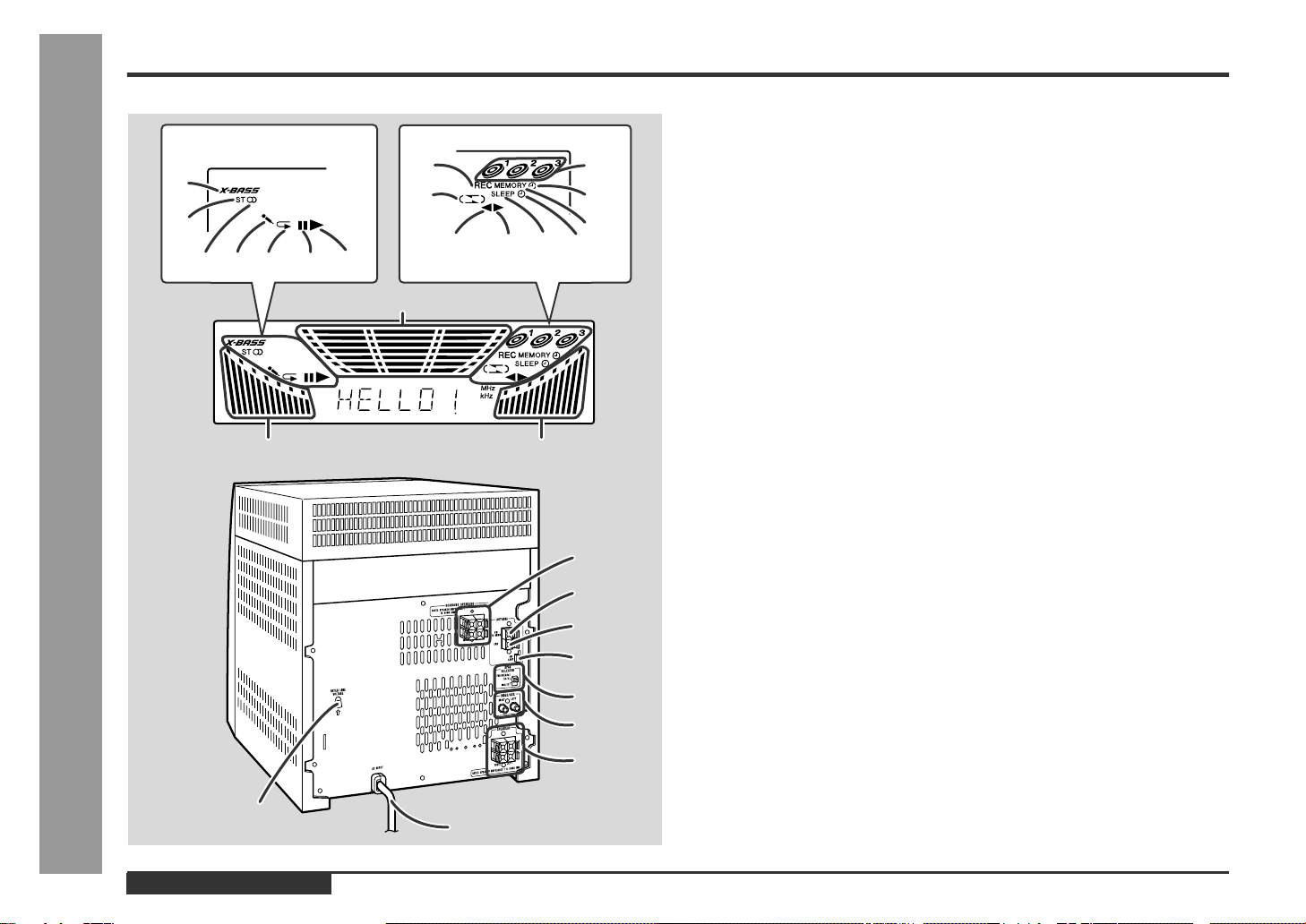
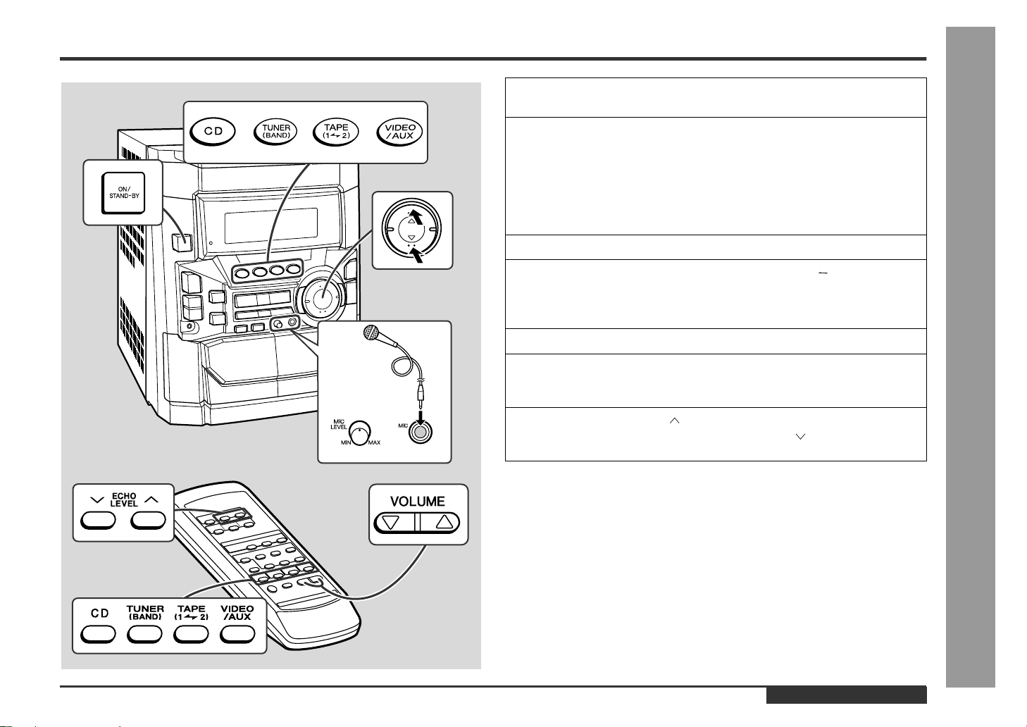
NAMES OF PARTS
CD-BK250W/CD-BK2600W/CD-BK270W
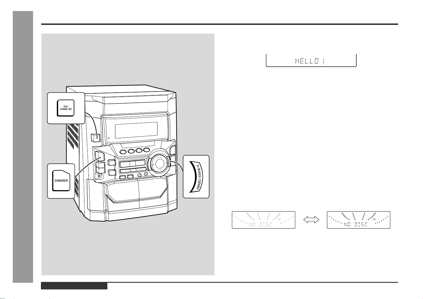
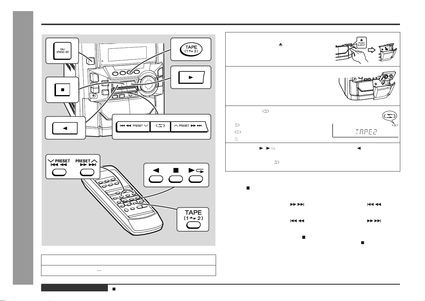
Front panel
1. Disc Tray
2. Timer Set Indicator
3. On/Stand-by Button
4. Tape 2 Cassette Compartment
5. Tape 1 Cassette Compartment
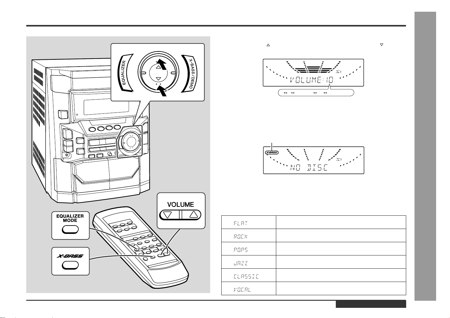
6. Equalizer Mode Select Button
7. Volume Up and Down Buttons
8. Extra Bass/Demo Mode Button
9. Disc Tray Open/Close Button
10. Disc Skip Button
11. Tuning and Time Up Button
12. Tape 2 Reverse Play Button
13. CD Button
14. Tuner (Band) Button
15. Tape (1 2) Button
16. Video/Auxiliary Button
17. Dimmer Button
18. Clock Button
19. Timer/Sleep Button
20. Headphone Socket
21. CD or Tape Stop Button
22. CD Play, Tape 1 Play or Tape 2 Forward Play Button
23. Tape 2 Reverse Mode Select Button
24. CD Track Up or Fast Forward, Tape 2 Fast Wind,
Tuner Preset Up Button
25. Tuning and Time Down Button
26. Memory/Set Button
27. Tape 2 Record Pause Button
28. CD Track Down or Fast Reverse, Tape 2 Fast Wind,
Tuner Preset Down Button
29. Microphone Level Control
30. Microphone Socket
17
22
21
161514131211
25 26 27
29 3028
23
24
18
19
20
4
5
6
1
2
3
8
9
10
7
Display
1. Extra Bass Indicator
2. FM Stereo Mode Indicator
3. FM Stereo Receiving Indicator
4. Karaoke Mode Indicator
5. CD Repeat Play Indicator
6. CD Pause Indicator
7. CD Play Indicator
8. Tape 2 Record Indicator
9. Tape Reverse Mode Indicator
10. Disc Number Indicators
11. Timer Play Indicator
12. Memory Indicator
13. Tape 2 Reverse Play Indicator
14. Tape 1 Play or Tape 2 Forward Play Indicator
15. Sleep Indicator
16. Timer Recording Indicator
17. Spectrum Analyser/Volume Level Indicator
1
2
34 5 6
8
9
17
17 17
13 14 15 16
7
10
11
12
CD-BK250W/CD-BK2600W/CD-BK270W
– 5 –
CD-BK250W/CD-BK2600W/CD-BK270W
CD-BK250W/CD-BK2600W
CD-BK270W
Rear panel
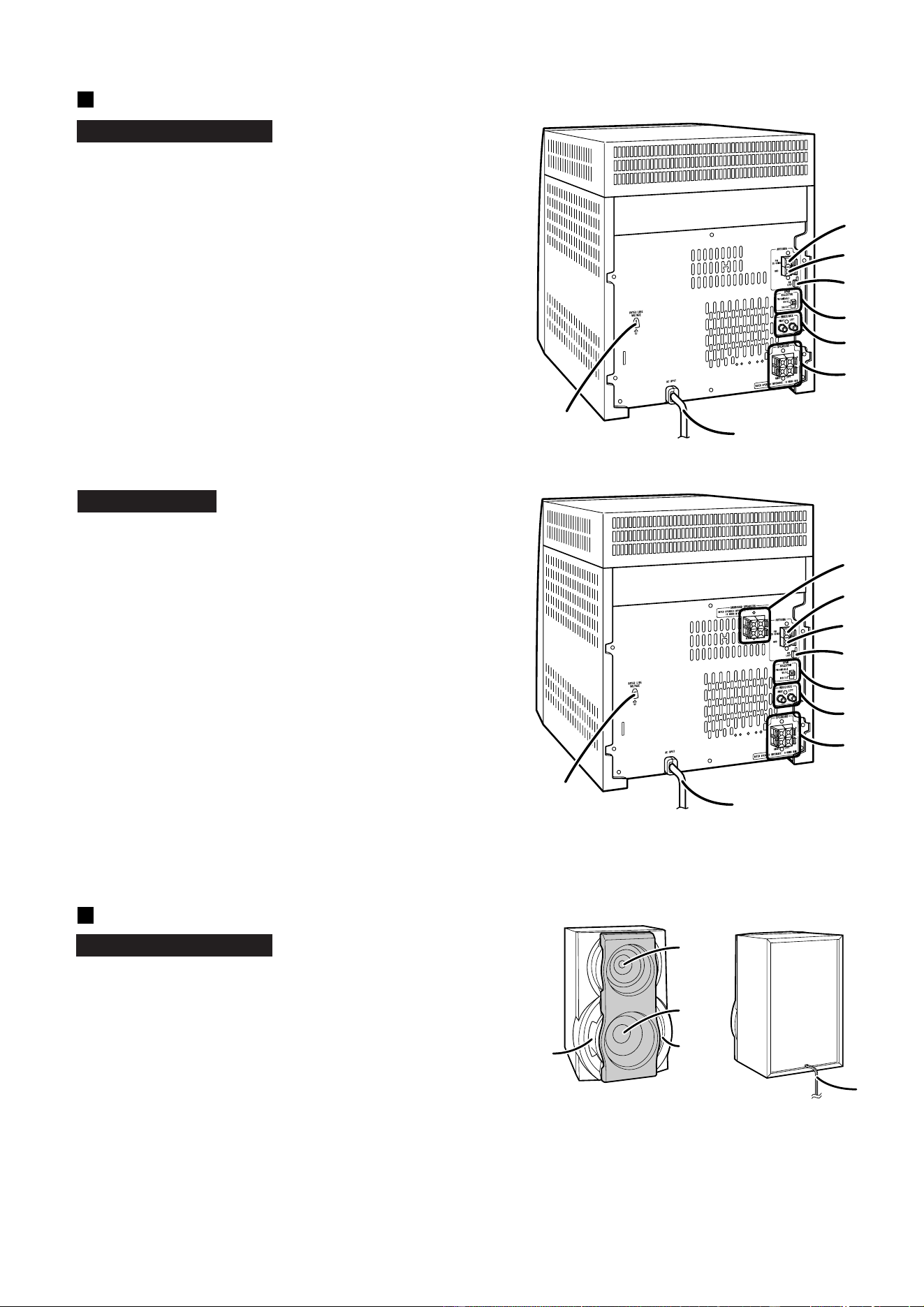
1. FM 75 Ohms Aerial Terminal
2. FM Aerial Earth Terminal
3. AM Loop Aerial Socket
4. Span Selector Switch
5. Video/Auxiliary (Audio Signal) Input Sockets
6. Speaker Terminals
7. AC Power Lead
8. AC Voltage Selector
2
1
5
6
7
4
3
8
1. Surround Speaker Terminals
2. FM 75 Ohms Aerial Terminal
3. FM Aerial Earth Terminal
4. AM Loop Aerial Socket
5. Span Selector Switch
6. Video/Auxiliary (Audio Signal) Input Sockets
7. Front Speaker Terminals
8. AC Power Lead
9. AC Voltage Selector
2
1
5
6
7
8
4
3
9
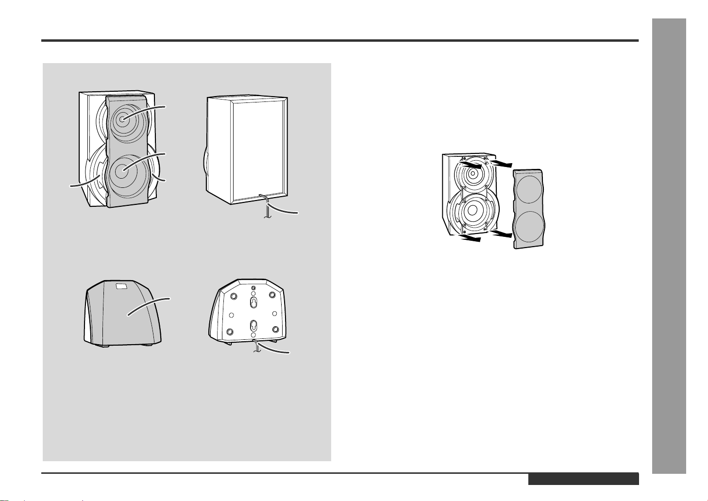
Speaker system
1. Tweeter
2. Woofer
3. Bass Reflex Duct
4. Speaker Wire
3
4
1
2
3
CP-BK250/CP-BK2600
CD-BK250W/CD-BK2600W/CD-BK270W
– 6 –
Front speaker
1. Tweeter
2. Woofer
3. Bass Reflex Duct
4. Speaker Wire
Surround speaker (CD-BK270W Only)
1. Full-Range Speaker
2. Speaker Wire
3
4
1
2
3
1
2
Remote control
1. Remote Control Transmitter
2. Echo Level Up and Down Buttons
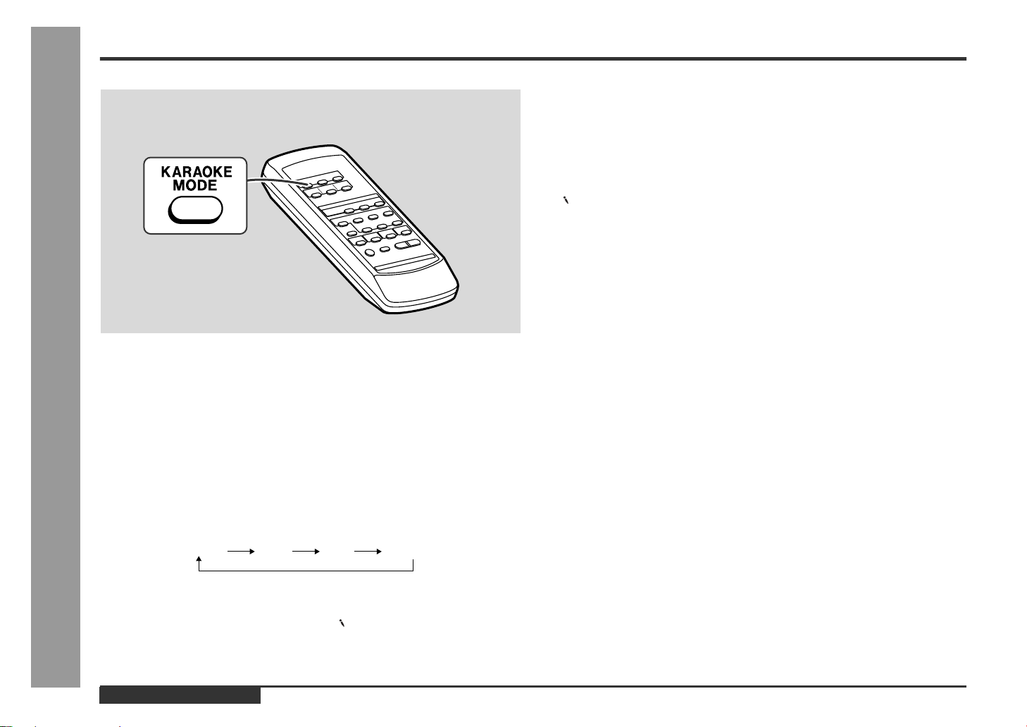
3. Karaoke Mode Button
4. Disc Number Select Buttons
5. CD Clear Button
6. Tape 2 Record Pause Button
7. CD Track Down or Fast Reverse, Tape 2 Fast Wind,
Tuner Preset Down Button
8. Equalizer Mode Select Button
9. Tape 2 Reverse Play Button
10. CD Button
11. Tuner (Band) Button
12. On/Stand-by Button
13. Extra Bass Button
14. CD Random Button
15. CD Memory Button
16. CD Pause Button
17. CD Track Up or Fast Forward, Tape 2 Fast Wind,
Tuner Preset Up Button
18. CD or Tape Stop Button
19. CD Play or Repeat, Tape 1 Play,
Tape 2 Forward Play Button
20. Video/Auxiliary Button
21. Tape (1 2) Button
22. Volume Up and Down Buttons
1
2
15
16
17
18
19
20
22
3
6
4
7
8
9
10
13
12
11
5
14
21
Buttons with " " mark in the illustration can be operated on the remote control
only.
Other buttons can be operated both on the main unit and the remote control.
GBOXS0070AWM1
CP-BK270
CD-BK250W/CD-BK2600W/CD-BK270W
– 7 –
CD-BK250W/CD-BK2600W/CD-BK270W
OPERATION MANUAL
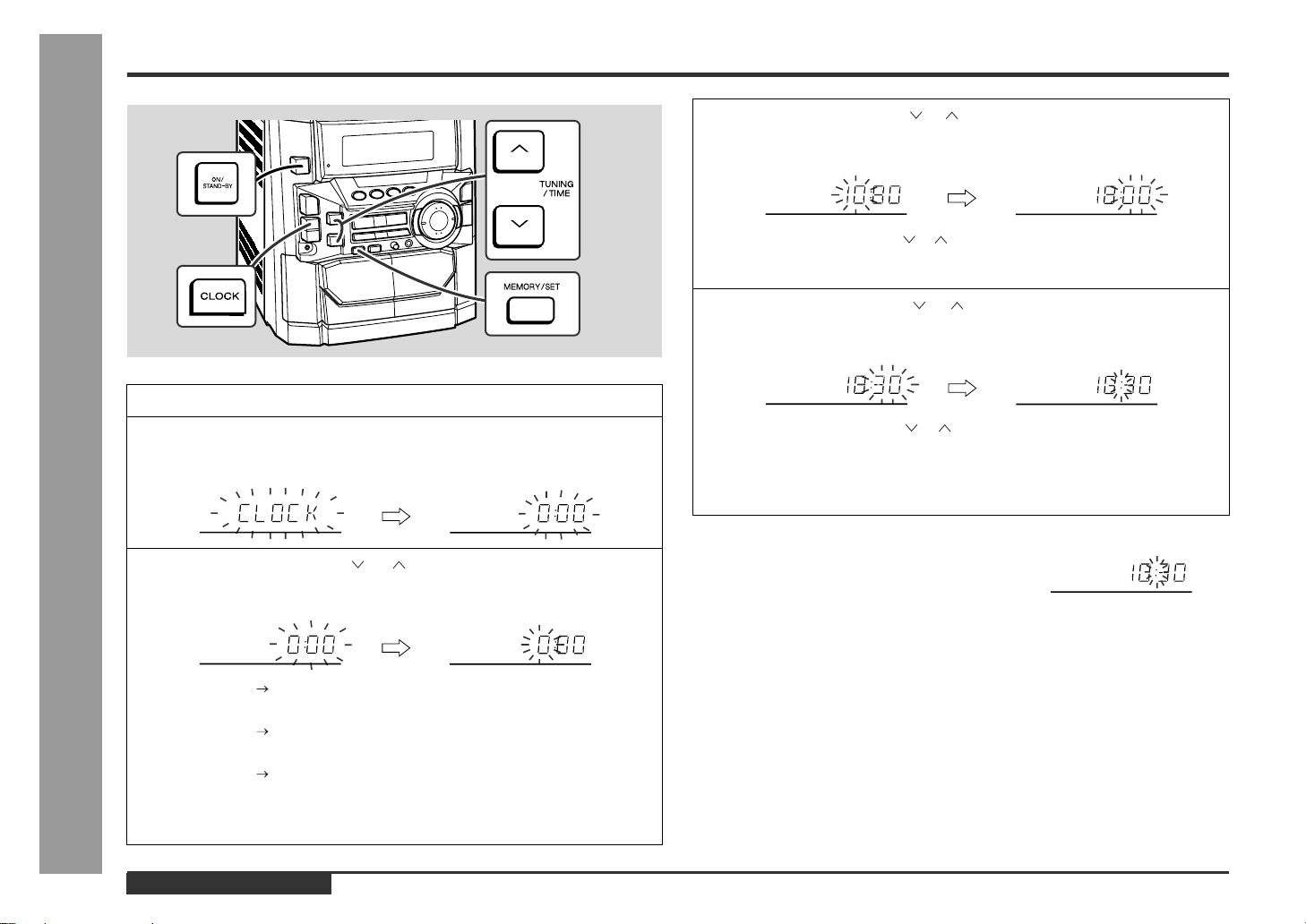
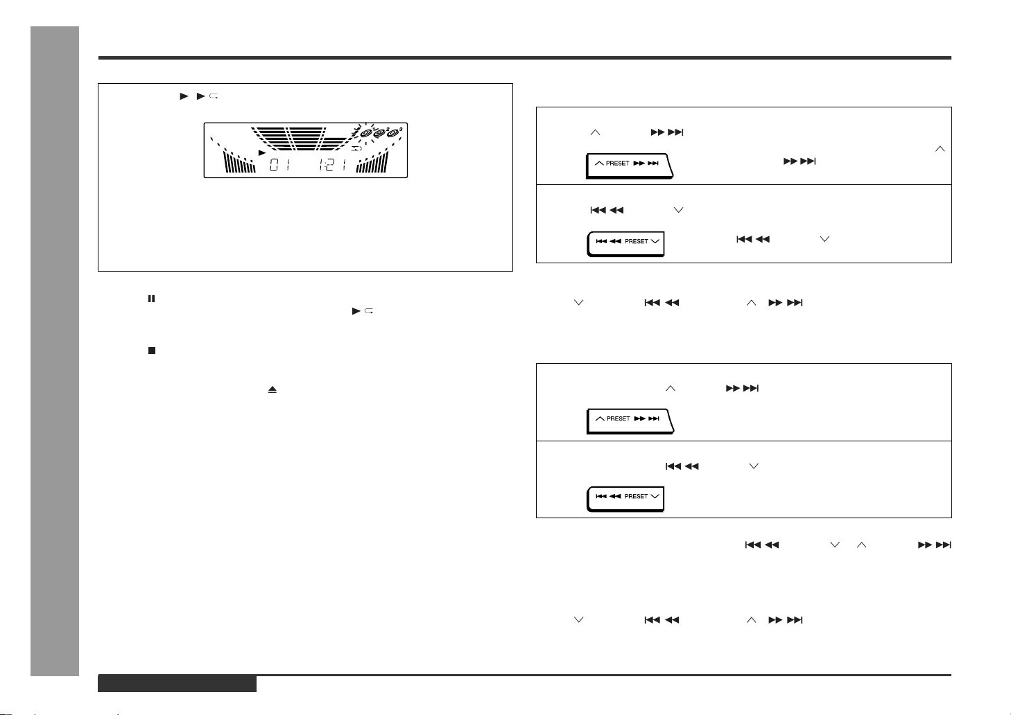
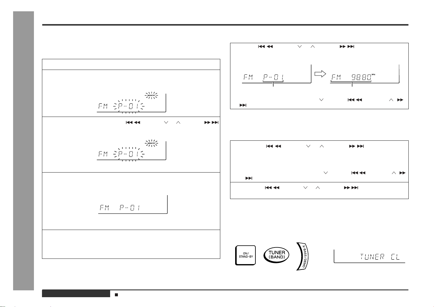
Setting the Clock
In this example, the clock is set for the 24-hour (0:00) display.
Note:
The "CLOCK" or time will flash at the push of the CLOCK button when the AC power
supply is restored after a power failure or unplugging the unit.
Readjust the clock as follows.
To readjust the clock:
Perform "Setting the Clock" from the beginning. If the time display is flashing, step 3
(for selecting the 24-hour or 12-hour display) will be skipped.
To change the 24-hour or 12-hour display:
1
Press the ON/STAND-BY button to turn the power on.
2
Press the CLOCK button and within 5 seconds, press the MEMO-
RY/SET button.
3
Press the TUNING/TIME ( or ) button to select 24-hour or 12-
hour display and then press the MEMORY/SET button.
"0:00" The 24-hour display will appear.
(0:00 - 23:59)
"AM 12:00" The 12-hour display will appear.
(AM 12:00 - PM 11:59)
"AM 0:00" The 12-hour display will appear.
(AM 0:00 - PM 11:59)
Note that this can only be set when the unit is first installed or it has been reset.
[Refer to "Clearing all the memory (reset)".]
4
Press the TUNING/TIME ( or ) button to adjust the hour and then
press the MEMORY/SET button.
Press the TUNING/TIME ( or ) button once to advance the time by 1 hour.
Hold it down to advance continuously.
When the 12-hour display is selected, "AM" will change automatically to "PM".
5
Press the TUNING/TIME ( or ) button to adjust the minutes and
then press the MEMORY/SET button.
Press the TUNING/TIME ( or ) button once to advance the time by 1
minute. Hold it down to change the time in 5-minute intervals.
The hour will not advance even if minutes advance from "59" to "00".
The clock begins counting from "0" seconds. (Seconds are not displayed.)
The time display will disappear after a few seconds.
To confirm the time display:
Press the CLOCK button.
The time display will appear for about 5 seconds.
1 Clear all the programmed contents. [Refer to "Clearing all the memory (reset)".]
2 Perform "Setting the Clock" from the beginning.
System Connections
Setting the AC voltage selector
Check the setting of the AC voltage selector located on the rear panel before plug-
ging the unit into an AC socket. If necessary, adjust the selector to correspond to the
AC power voltage used in your area.
Turn the selector with a screwdriver until the appropriate voltage num-
ber appears in the window (110 V, 127 V, 220 V or 230 V - 240 V AC).
Connecting the AC power lead
After making all connections, plug the unit. If you plug the unit first,
the unit will enter the demonstration mode.
Note:
Unplug the AC power lead from the AC socket if the unit will not be in use for a pro-
longed period of time.
AC Plug Adaptor
In areas (or countries) where an AC socket as shown in illustration is used, con-
nect the unit using the AC plug adaptor supplied with the unit, as illustrated. The AC
plug adaptor is not included in areas where the AC wall socket and AC power plug
can be directly connected (see illustration ).
1
2
Setting the FM/AM span selector
The International Telecommunication Union (ITU) has established that member coun-
tries should maintain either a 100 kHz or a 50 kHz interval between broadcasting fre-
quencies of FM stations and 10 kHz or 9 kHz for AM station. The illustration shows
the 50/9 kHz zones (regions 1 and 3), and the 100/10 kHz zone (region 2).
Before using the unit, set the SPAN SELECTOR switch (on the rear panel) to the
interval (span) of your area.
To change the tuning zone:
Caution:
This operation will erase all data stored in memory including clock, timer settings,
tuner preset, and CD programme.
1 Press the ON/STAND-BY button to enter the stand-by mode.
2 Set the SPAN SELECTOR switch (on the rear panel) as follows.
For 50 kHz FM interval (9 kHz in AM) 50/9
For 100 kHz FM interval (10 kHz in AM) 100/10
3 Whilst pressing down the button and the X-BASS/DEMO button, press the ON/
STAND-BY button until "CLEAR AL" appears.
CD-BK250W/CD-BK2600W/CD-BK270W
– 8 –
Troubleshooting Chart
Many potential "problems" can be resolved by the owner without calling a service
technician.
If something is wrong with this product, check the following before calling your autho-
rised SHARP dealer or service centre.
General
CD player
Tuner
Cassette deck
Karaoke
Remote control
Symptom Possible cause
The clock is not on time. Did a power failure occur? Reset the
clock.
When a button is pressed, the unit
does not respond.
Set this unit to the power stand-by mode
and then turn it back on.
If the unit still malfunctions, reset it.
No sound is heard. Is the volume level set to "0"?
Are the headphones connected?
Are the speaker wires disconnected?
Is the karaoke mode set to "L-CH", "R-CH"
or "V-CANCEL"?
Symptom Possible cause
Playback does not start. Is the disc loaded upside down?
Playback stops in the middle or is
not performed properly.
Does the disc satisfy the standards?
Is the disc distorted or scratched?
Playback sounds are skipped, or
stopped in the middle of a track.
Is the unit located near excessive vibra-
tions?
Is the disc very dirty?
Has condensation formed inside the unit?
Symptom Possible cause
Radio makes unusual noise con-
secutively.
Is the unit placed near the TV or comput-
er?
Is the FM aerial or AM loop aerial placed
properly? Move the AC power lead away
from the aerial if located near.
Symptom Possible cause
Cannot record. Is the erase-prevention tab removed?
Cannot record tracks with proper
sound quality.
Is it a normal tape? (You cannot record on
a metal or CrO tape.)
Cannot erase completely.
Sound skipping. Is there any slack?
Is the tape stretched?
Cannot hear treble. Are the capstans, pinch rollers, or heads
dirty?
Sound fluctuation.
Cannot remove the tape. If a power failure occurs during playback,
the heads remain engaged with the tape.
Do not open the compartment forcibly.
Wait until electricity resumes.
Symptom Possible cause
The vocal part of a multiplexed
disc is not heard.
Is the karaoke mode set to "L-CH", "R-CH"
or "V-CANCEL"?
Symptom Possible cause
The remote control does not oper-
ate.
Is the AC power lead of the unit plugged
in?
Is the battery polarity respected?
Are the batteries dead?
Is the distance or angle incorrect?
Does the remote control sensor receive
strong light?
Troubleshooting Chart
If trouble occurs
When this product is subjected to strong external interference (mechanical shock,
excessive static electricity, abnormal supply voltage due to lightning, etc.) or if it is
operated incorrectly, it may malfunction.
If such a problem occurs, do the following:
1 Set the unit to the stand-by mode and turn the power on again.
2 If the unit is not restored in the previous operation, unplug and plug in the unit,
and then turn the power on.
Note:
If neither operation above restores the unit, clear all the memory by resetting it.
Clearing all the memory (reset)
1 Press the ON/STAND-BY button to enter the power stand-by mode.
2 Whilst pressing down the button and the X-BASS/DEMO button, press the ON/
STAND-BY button until "CLEAR AL" appears.
Caution:
This operation will erase all data stored in memory including clock, timer settings,
tuner preset, and CD programme.
Before transporting the unit
1 Press the ON/STAND-BY button to turn the power on.
2 Press the CD button.
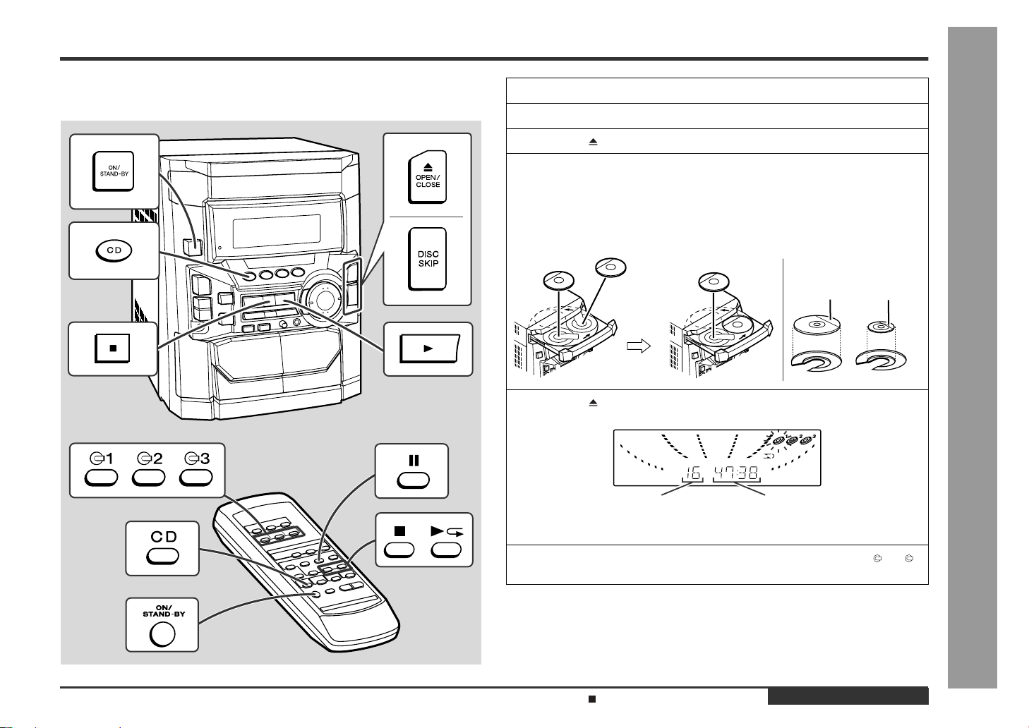
3 Press the OPEN/CLOSE button to open the disc tray.
Remove all CDs inserted in the unit.
4 Press the OPEN/CLOSE button to close the disc tray.
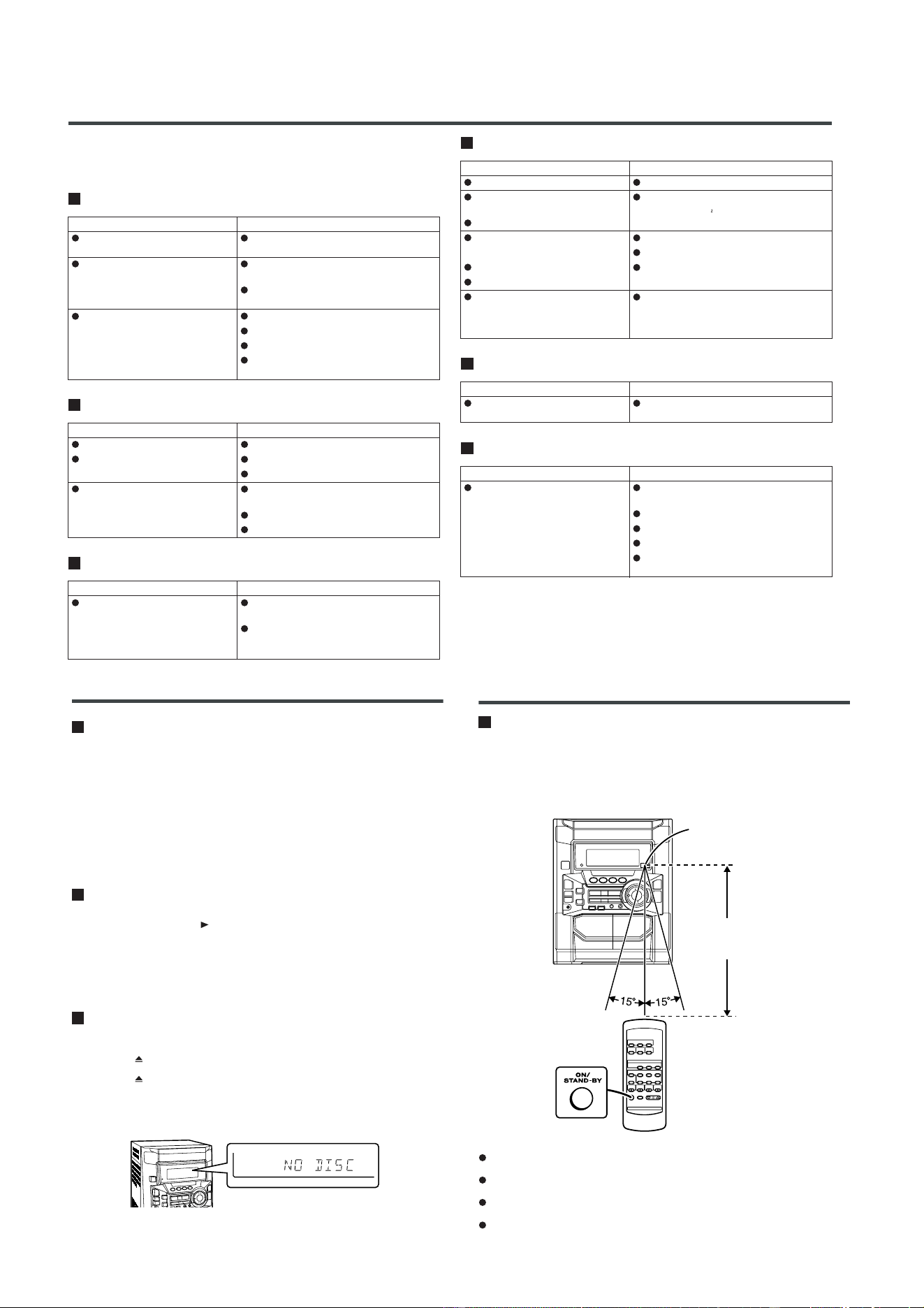
Make sure that "NO DISC" is displayed.
5 Press the ON/STAND-BY button to enter the stand-by mode, and then unplug
the AC power lead from the AC socket.
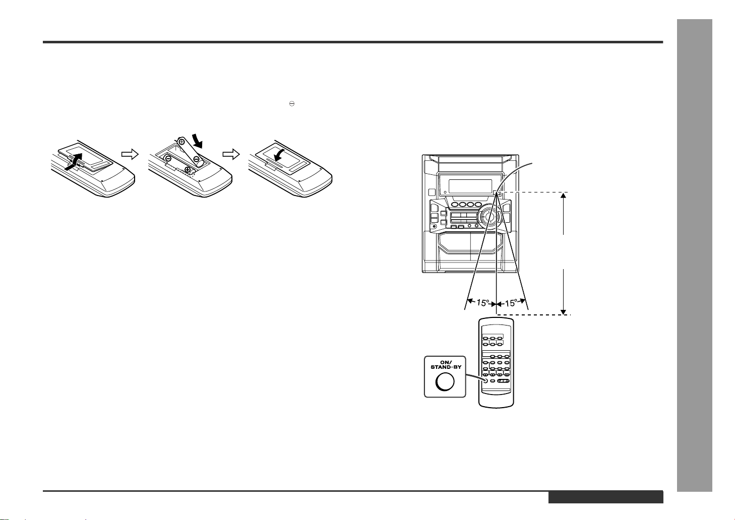
Remote Control
Notes concerning use:
Replace the batteries if the operating distance is reduced or if the operation
becomes erratic. Purchase 2 "AA" size batteries (UM/SUM-3, R6, HP-7 or similar).
Periodically clean the transmitter on the remote control and the sensor on the unit
with a soft cloth.
Exposing the sensor on the unit to strong light may interfere with operation.
Change the lighting or the direction of the unit.
Keep the remote control awa
y
from moisture, heat, shock, and vibrations.
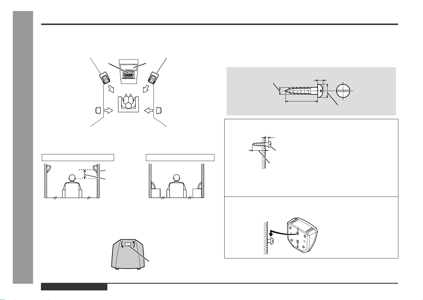
Test of the remote control
Face the remote control directly to the remote sensor on the unit.
The remote control can be used within the range shown below:
Press the ON/STAND-BY button. Does the power turn on? Now, you can enjoy the
music.
0.2 m - 6 m
(8" - 20')
Remote sensor
– 9 –
CD-BK250W/CD-BK2600W/CD-BK270W
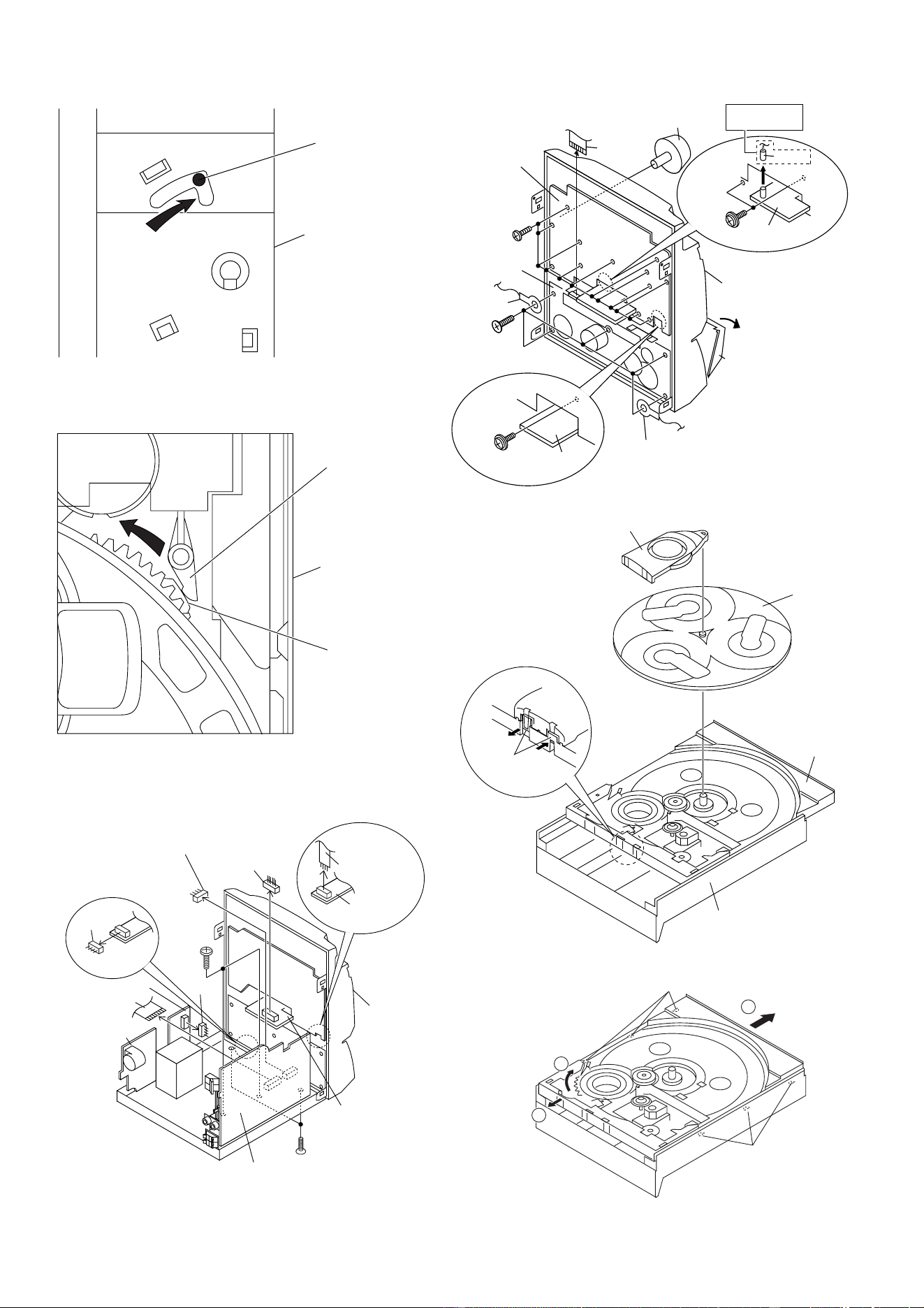
1 Top Cabinet 1. Screw ...................... (A1) x4 9-1
2 Side Panel 1. Screw ...................... (B1) x8 9-1
(Left/Right)
3 CD Player Unit/ 1. Turn on the power supply, .. 9-2
CD Tray Cover open the disc tray, take out
the CD tray cover, and close.
(Note 1)
2. Screw ...................... (C1) x1
3. Hook ........................ (C2) x3
4. Hook ........................ (C3) x2
5. Socket ..................... (C4) x2
4 Rear Panel with 1. Screw .................... (D1) x11 9-2
Fan Motor
(For CD-BK250W/CD-BK2600W)
1. Screw .................... (D1) x14
(For CD-BK270W)
2. Socket ..................... (D2) x1
(For CD-BK250W/CD-BK2600W)
2. Socket ..................... (D2) x2
(For CD-BK270W)
5 Main PWB 1. Screw ...................... (E1) x3
9-2,10-3
2. Socket ..................... (E2) x4 10-3
3. Flat Cable ............... (E3) x1
4. Flat Wire.................. (E4) x1
6 Front Panel 1. Screw .......................(F1) x2 10-3
7 Display PWB 1. Knob ........................ (G1) x1 10-4
2. Screw .................... (G2) x12
3. Flat Cable ............... (G3) x1
8 Tape Mechanism 1. Open the cassette holder. .. 10-4
2. Screw...................... (H1) x5
9
Headphones PWB
1. Screw ....................... (J1) x1 10-4
10 Mic PWB 1. Screw ...................... (K1) x2 10-4
2. Tip ........................... (K2) x1
(CD-BK270W Only)
11 Turntable 1. Hook ......................... (L1) x2 10-5
2. Cover ....................... (L2) x1
12 Disc Tray 1.
Turn fully the lock lever in the
10-1
arrow direction
.
2.
While holding the lock lever,rotate
10-2
the cam gear until the cam gear
rib engages with the clamp lever.
3.
Push the slide chassis backward
10-6
to engage the claw with the
groove and remove it in the
direction of the arrow
..
(M1) x6
13 CD Servo PWB 1. Screw ...................... (N1) x1 11-1
(Note 2) 2. Hook ........................ (N2) x2
3. Socket ..................... (N3) x4
14 CD Mechanism 1. Hook ........................ (P1) x2 11-2
2. Hook ........................ (P2) x3
DISASSEMBLY
Caution on Disassembly
Follow the below-mentioned notes when disassembling
the unit and reassembling it, to keep it safe and ensure
excellent performance:
1. Take cassette tape and compact disc out of the unit.
2. Be sure to remove the power supply plug from the wall
outlet before starting to disassemble the unit.
3. Take off nylon bands or wire holders where they need to
be removed when disassembling the unit. After servicing
the unit, be sure to rearrange the leads where they were
before disassembling.
4. Take sufficient care on static electricity of integrated
circuits and other circuits when servicing.
Figure 9-2
CD-BK250W/CD-BK2600W/CD-BK270W
STEP
REMOVAL
PROCEDURE
FIGURE
Figure 9-1
CD-BK250W/CD-BK2600W/CD-BK270W
Note 1: How to open the changer manually. (Fig. 10-1)
1. In this state, turn fully the lock lever in the arrow direction through
the hole on the loading chassis bottom.
2.
While holding the lock lever, rotate the cam gear anticlockwise until the
cam gear rib engages with the clamp lever.
(Fig. 10-2)
3. After that, push forward the slide chassis.
Note 2:
1. After removing the connector for the optical pickup from the
connector, wrap the conductive aluminium foil around the front end
of the connector so as to protect the optical pickup from electro-
static damage.
Note 3:
1. Be careful not to break the claw of the CD mechanism.
2. When fining back the cam gear assembly, let it lock by front
movement.
Illustration: CD-BK270W
(B1)x4
ø3x10mm
(B1)x2
ø3x10mm
Rear
Panel
(B1)x2
ø3x10mm
Side Panel
(Right)
Side Panel
(Left)
(A1)x2
ø3x12mm
(A1)x2
ø3x12mm
Top Cabinet
Pull
Pull
(C3)x1
(C4)x2
CD Servo
PWB
CD Tray Cover
(C2)x3
1
1
2
(C3)x1
CD Player
Unit
(E1)x1
ø3x10mm
Lug Wire
(D1)x2
ø3x10mm
Main PWB
(C1)x1
ø3x10mm
(D1)x9
ø3x10mm
(D1)x3
ø3x10mm
Rear
Panel
(D2)x1
(D2)x1
CD-BK270W
ONLY
CD-BK270W
ONLY
CD-BK250W/CD-BK2600W/CD-BK270W
– 10 –
Figure 10-1
Figure 10-2
Figure 10-3
Figure 10-4
Figure 10-5
Figure 10-6
Lock Lever
CD Player Unit
(Bottom View)
Clamp Lever
CD Player Unit
(Top View)
Cam Gear Rib
Transformer
PWB
(E3)x1
Power PWB
(E2)x1
(E1)x2
ø3x10mm
(E2)x1
(E2)x1
(E2)x1
Headphones
PWB
(E4)x1
Mic PWB
Front
Panel
(F1)x2
ø3x8mm
Main PWB
(G3)x1
(G1)x1
(K2)x1
Mic PWB
(K1)x2
ø3x10mm
Open
Cassette
Holder
Lug Wire
Lug Wire
Headphones
PWB
(J1)x1
ø3x10mm
(H1)x5
ø3x10mm
Tape
Mechanism
(G2)x12
ø3x10mm
Display
PWB
CD-BK270W
ONLY
Front
Panel
Turntable
Slide
Chassis
(L2)x1
CD Player Unit
(L1)x2
3
(M1)x3
(M1)x3
1
2
– 11 –
CD-BK250W/CD-BK2600W/CD-BK270W
1 Front Panel 1. Net.......................... (A1) x1 11-3
2 Woofer 1. Screw ..................... (B1) x4 11-4
3 Tweeter 1. Screw ..................... (C1) x2 11-4
STEP
REMOVAL PROCEDURE
FIGURE
Figure 11-3
Figure 11-1
CP-BK250/CP-BK2600/CP-BK270
Figure 11-4
(A1)x1
Screwdriver
Driver should
be pried away
from Speaker Box.
Front Panel
Speaker Box
(B1)x4
ø4x12mm
Woofer
(C1)x2
ø3x10mm
Tweeter
Figure 11-2
(N3)x2
(N2)x2
(N3)x2
CD Servo
PWB
Slide
Chassis
(N1)x1
ø3x8mm
(P2)x3
(P1)x1
(P1)x1
CD
Mechanism
Slide
Chassis
CD-BK250W/CD-BK2600W/CD-BK270W
– 12 –
REMOVING AND REINSTALLING THE MAIN PARTS
TAPE MECHANISM SECTION
Perform steps 1 to 6 and 8 of the disassembly method to
remove the tape mechanism.
How to remove the record/playback and erase
heads (TAPE 2) (See Fig. 12-1)
1. When you remove the screws (A1) x 2 pcs., the recording/
playback head and three-dimensional head of the erasing
head can be removed.
How to remove the playback head (TAPE 1)
(See Fig. 12-2)
1. When you remove the screws (B1) x 2 pcs., the playback
head.
How to remove the pinch roller (TAPE 1/2)
(See Fig. 12-3)
1. Carefully bend the pinch roller pawl in the direction of the
arrow <A>, and remove the pinch roller (C1) x 1 pc., in the
direction of the arrow <B>.
Note:
When installing the pinch roller, pay attention to the spring
mounting position.
How to remove the belt (TAPE 2) (See Fig. 12-4)
1. Remove the main belt (D1) x 1 pc., from the motor side.
2. Remove the FF/REW belt (D2) x 1 pc.
How to remove the belt (TAPE 1) (See Fig. 12-4)
1. Remove the main belt (E1) x 1 pc., from the motor side.
2. Remove the FF/REW belt (E2) x 1 pc.
How to remove the motor (See Fig. 12-5)
1. Remove the screws (F1) x 2 pcs., to remove the motor.
Figure 12-1
Figure 12-2
Figure 12-3
Figure 12-4Figure 12-5
(A1)x2
Ø2x6mm
TAPE 2
Record/Playback
Head
Erase Head
Clutch Ass'y
(B1)x1
Ø2x9mm
(B1)x1
Ø2x5mm
TAPE 1
Playback
Head
Clutch Ass'y
Pinch Roller
(C1)x1
<A>
Pull
<B>
Pull
Pinch
Roller
Pawl
TAPE 2
TAPE 1
Main Belt
(E1)x1
TAPE 2
Main Belt
(D1)x1
TAPE 1
FF/REW
Belt
(D2)x1
FF/REW
Belt
(E2)x1
Motor
Motor
Main Belt
(D1)x1
Main Belt
(E1)x1
(F1)x2
Ø2.6x5mm
Motor
Clutch Ass'y
– 13 –
CD-BK250W/CD-BK2600W/CD-BK270W
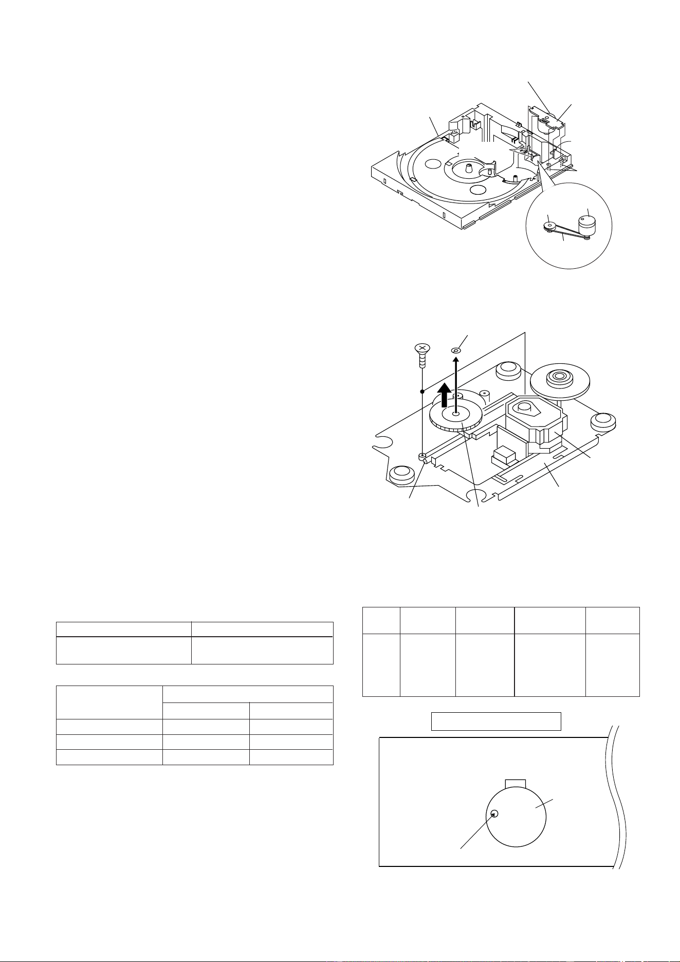
How to remove the pickup (See Fig. 13-2)
1. Remove the stop washer (B1) x 1 pc., to remove the gear
(B2) x 1 pc.
2. Remove the screws (B3) x 2 pcs., to remove the shaft
(B4) x 1 pc.
3. Remove the pickup.
Note
After removing the connector for the optical pickup from the
connector wrap the conductive aluminium foil around the front
end of connector so as to protect the optical pickup from
electrostatic damage.
Figure 13-2
CD MECHANISM SECTION
Perform steps 1, 2, 3, 11,12, 13 and 14 of the disassembly
method to remove the CD mechanism.
How to remove the loading motor
(See Fig. 13-1)
1. Bend the hooks (A1) x 5 pcs., to remove the loading motor.
2. Remove the drive belt (A2) x 1pc.
Figure 13-1
ADJUSTMENT
MECHANISM SECTION
• Driving Force Check
Torque Meter Specified Value
Play: TW-2111 Tape 1: Over 80 g
Tape 2: Over 80 g
• Torque Check
Torque Meter
Tape 2
Play: TW-2111 30 to 80 g.cm 30 to 80 g.cm
Fast forward: TW-2231 — 70 to 180 g.cm
Rewind: TW-2231 — 70 to 180 g.cm
Specified Value
Tape 1
Specified
Value
Adjusting
Point
Instrument
Connection
Test Tape
Normal MTT-111 Variable 3,000 ± 30 Hz Speaker
speed Resistor in Terminal
motor. (Load
resistance:
6 ohms)
• Tape Speed
Figure 13-3
(A1)x2
(A1)x1
Loading Motor
Loading
Motor PWB
Slide
Chassis
(A1)x2
Pulley
Drive Belt
(A2)x1
Loading
Motor
(B3)x2
ø2.6x6mm
Shaft
(B4)x1
Stop Washer
(B1)x1
Gear
(B2)x1
CD Mechanism
Pickup
TAPE MECHANISM
Tape
Motor
Variable Resistor in motor
CD-BK250W/CD-BK2600W/CD-BK270W
– 14 –
Figure 14-2
CD ERROR CODE DESCRIPTION
Error
State Code
[Servo System Error]
0001 Cannot detect Pickup-in SW
0002 DSP access error
[Error during close operation]
0101 Open/Close SW not functioning (Low → High)
0103 Open/Close SW not functioning (High → Low)
[Error during open operation]
0201 Open/Close SW not functioning (Low → High)
0203 Open/Close SW not functioning (High → Low)
[Error during skip operation]
0302 Pickup-in SW is not detected
0306 During Disc 1 search, Open/Close SW or Clamp SW
or Disc SW do not change to low.
0307 Clamp SW not function (Low → High)
0308 Clamp SW not function (High → Low)
T
T
EFBL
FDO
TE
Stopped
CH1=500 mV
DC 10:1
CH2=200 mV
DC 10:1
CH3=1 V
DC 10:1
500 ms/div
(500 ms/div)
NORM:20 kS/s
1
2
3
=Record Length=
Smoothing : ON CH1 : 0.000 V
CH2 : 0.000 V
Main : 100K
Zoom : 2k
Mode : SINGLE
Type : EDGE CH1
Delay : 0.0 ns
Hold off : 0.2 µs
CH3 : 0.00 V
CH4 : 0.00 V
BW : FULL
=Trigger==Filter= =Offset=
CH2
v/DIV
200 mV
1999/04/05 20:26:47
Test Stage
Frequency Frequency
Display
Setting/
Adjusting
Parts
Instrument
Connection
CD SECTION
• AM IF/RF
Signal generator: 400 Hz, 30%, AM modulated
*1. Input: Antenna Output: TP302
*2. Input: Antenna Output: TP301
TUNER SECTION
fL: Low-range frequency
fH: High-range frequency
AM IF 450 kHz 1,602 kHz T351 *1
AM Band — 531 kHz (fL): T306 *2
Coverage 1.1 ± 0.1 V
AM Tracking 990 kHz 990 kHz (fL): T303 *1
*1. Input: Antenna Output: TP301
*2. Input: Antenna Output: Speaker terminal
• FM RF
Signal generator: 1 kHz, 40 kHz dev., FM modulated
FM Band — 87.50 MHz T301(fL): *1
Coverage 1.3 V ± 0.1 V
FM RF 98.00 MHz 98.00 MHz L312 *2
(10-30 dB)
Test Stage
Instrument
Connection
Frequency Frequency
Display
Setting/
Adjusting
Point
Figure 14-1 ADJUSTMENT POINTS
Items adjusted automatically
(1) Offset adjustment (The offset voltage between the head
amplifier output and the VREF reference voltage is
compensated inside the IC.)
* Focus offset adjustment
* Tracking offset adjustment
(2) Tracking balance adjustment (waveform drawing
Fig.14-2 EFBL)
(3) Gain adjustment (The gain is compensated inside the IC
so that the loop gain at the gain crossover frequency will
be 0 dB.)
* Focus gain adjustment
* Tracking gain adjustment
• Adjustment
Since this CD system incorporates the following automatic
adjustment functions, readjustment is not needed when
replacing the pickup. Therefore, different PWBs and pickups
can be combined freely.
Each time a disc is changed, these adjustments are
performed automatically. Therefore, playback of each disc
can be performed under optimum conditions.
IC301
AM IF
FM IF
FM RF
T303
T306
T302
L312
AM
TRACKING fL
AM BAND
COVERAGE fL
T301
T351
FM BAND
COVERAGE fL
MAIN PWB
CNP301
AM LOOP
ANTENNA
SO302
FM ANTENNA
TERMINAL
TP302
R357
R316
TP301
– 15 –
CD-BK250W/CD-BK2600W/CD-BK270W
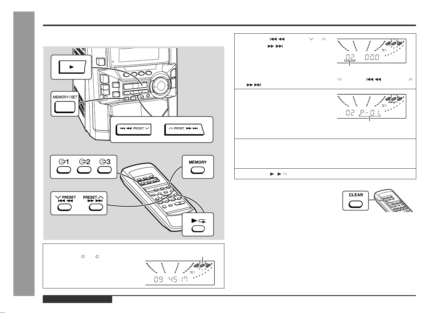
TEST MODE
• Setting the test mode
Any one of test mode can be set by pressing several keys as follows.
<X-BASS> + <CD> + <POWER> TEST:CD operation test
Function: -CD test mode.
-Enter test mode.
C D T E S T
OPEN/CLOSE operation is using manual.
<< >>, << >> buttons make pick's slide possible.
Do TOC IL. Do normal play
When these following key is input
into PLAY key, track number can
be appoint directly
<<PLAY>> key input.
<<MEMORY>> key input.
<< 1>> key: Track 4
<<
2>> key: Track 9
<<
3>> key: Track 15
<<STOP>> key input.
STOP
Laser ON.
<<MEMORY>> key input.
Tracking OFF play at that
specific point.
<<MEMORY>> key input.
Tracking ON play from
that specific point.
<<STOP>> key input.
STOP
IL isn't done
VOL — Last memory
BAL — CENTER
P.GEQ — FLAT
X-BASS — OFF
To cancel : Power OFF
Sliding the PICKUP with
<< >>, << >> button
must only be in STOP mode.
<<MEMORY>>
key input
Adjustment result
automatically will
display as below
for each 2 sec :
a) "FOFF_XX"
b) "TOFF_XX"
c) "TBAL_XX"
d) "TGAN_XX"
f) "FGAN_XX"
g) "RFLS_XX"
explanation:
a) Focus off set = "FOFF_XX"
b) Tracking off set = "TOFF_XX"
c) Tracking balance = "TBAL_XX"
d) Tracking gain = "TGAN_XX"
f) Focus Gain = "FGAN_XX"
g) RF level shift = "RFLS_XX"
Adjustment result auto-
matically will display as
below
for each 2 sec :
a) "FOFF_XX"
b) "TOFF_XX"
c) "TBAL_XX"
d) "TGAN_XX"
f) "FGAN_XX"
g) "RFLS_XX"
XX: Hex value
CD-BK250W/CD-BK2600W/CD-BK270W
– 16 –
Standard Specification of Stereo System Error Message Display Contents
Error Contents DISPLAY Notes
Output while Device Protection Operation 'PROTECT' 00: While in Protect Circuit Operate
01: Over Current Detection
02: DC Detection
03:
TAPE Mechanism Error 'ER-TA**' 00: Tape Mechanism Error
01: Initial Error
02:
03:
CD/VCD Pickup Mechanism Error 'ER-CD**' 00: Pickup Mechanism Error
01: PU-IN SW Detection NG
02:
03:
04:
CD Changer Mechanism Error 'ER-CD**' 10: Changer Error
11: Initial Error
12:
13:
Tray Error 'ET-CD**' 20: Tray Error
21:
22:
23:
Focus Not Match 'NO DISC'
IL Time Over 'NOT READ'
TUN PLL Unlock 'ER-TU**' 00: TUN Error
01: PLL Unlock
02:
03:
– 17 –
CD-BK250W/CD-BK2600W/CD-BK270W
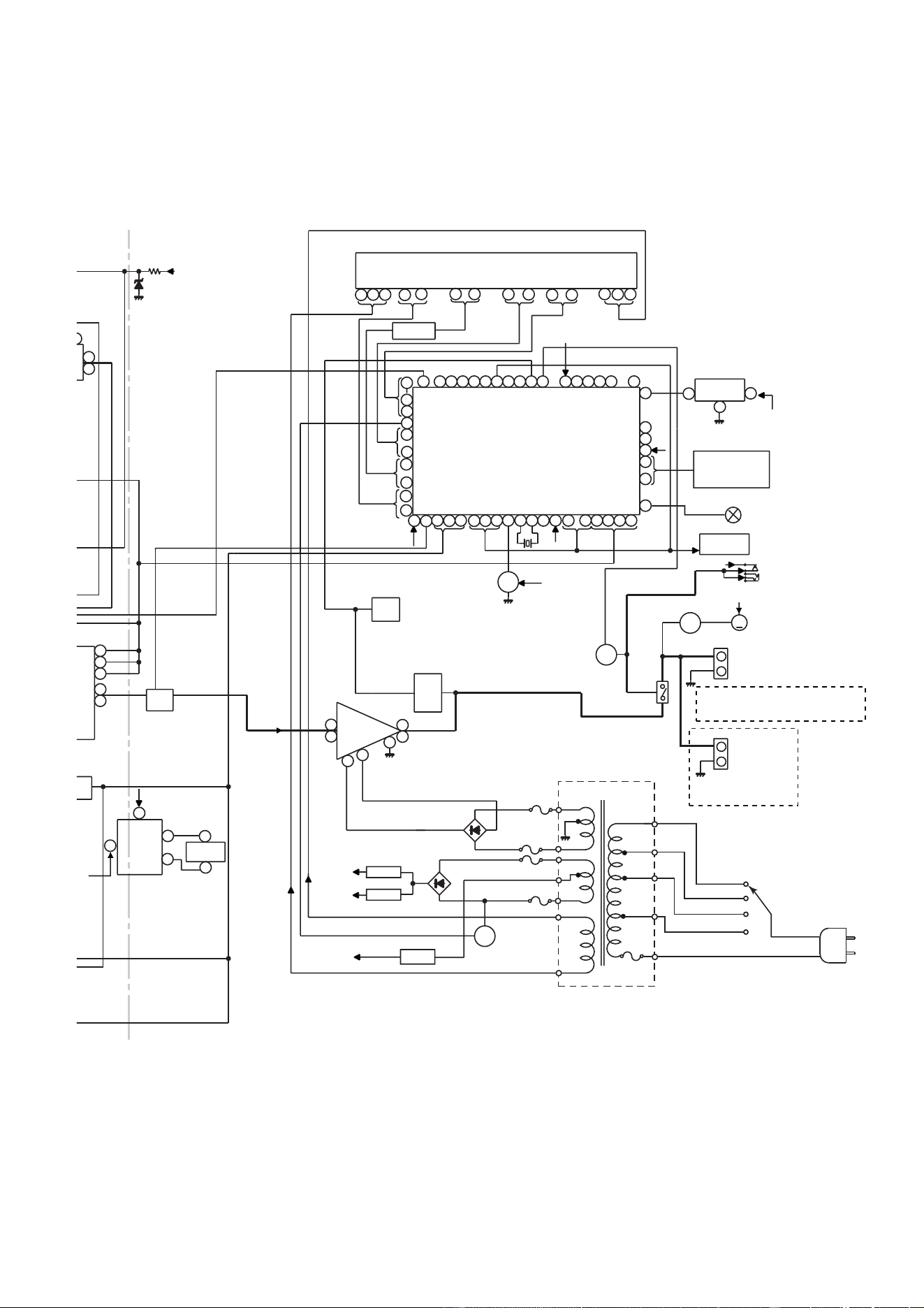
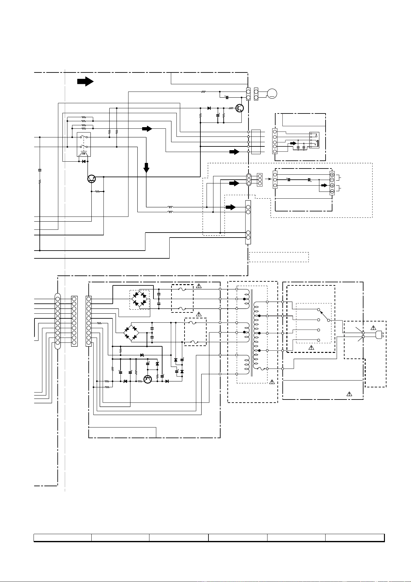
Figure 17 BLOCK DIAGRAM (1/3)
+5V
CNS4
BI4
CNP4
M3
T/T UP DOWN
LOADING
+3.3V
TO DISPLAY SECTION
TO MAIN SECTION
CONSTANT
VOLTAGE
Q2
LASER
DRIVER
+3.3V
+3.3V
Q1
+5V
PICK UP UNIT
IC1
LC78645E
CD SERVO
VVDD
LDD
LDS
M
SW3
DISC
NUMBER
SW2
CLAMP
SW1
OPEN/
CLOSE
CNP8
CNP7
TRACKING COIL
FOCUS COIL
SW4
PICKUP
IN
M2
SLED
MOTOR
M1
SPINDLE
MOTOR
M
M
R-CH
Q3
XVDD
RVDD
LVDD
ADAVDD
RFVDD
XL1
33.8688MHz
OC. DISC NO
CLAMP SW
CD RES
CLK
DI
DO
CE
DRF
WRQ
+5(+B5)
+5(+B5)
DGND
L-CH
AGND
VCC3
VCC2
VCC4
VCC1
IC2
M63001FP
FOCUS/TRACKING/
SPIN/SLED
DRIVER
XIN
XOUT
RES
WRQ
DO
DI
CLK
CE
TIN2
TIN1
FIN2
FIN1
TD0
FD0
SPDO
SLDO
CONT5
CONT2
CONT3
CONT4
RCHO
RVSS
LVSS
LCHO
80
42
79
75
20
5
40
18
24
23
14
8
21
22
29
35
41
47
46
7
10
987
15
12
17 25
42
41 8339
4765
16
82
26 27
316452
316452
316452
54
71
61
62
63
69
57
56
55
51
50
40
37
19
28
26
23
22
21
3271689
615432
4543 44 25 70
64
65
66
48
49
18
CD-BK250W/CD-BK2600W/CD-BK270W
– 18 –
Figure 18 BLOCK DIAGRAM (2/3)
AM
ANTENNA
SO302
FM
ANTENNA
CNP301
JK1
MIC
1
2
IC101
AN7345K
PLAYBACK AND RECORD
/PLAYBACK AMP.
AUX
R
L
R
L
JK690
VIDEO/AUX IN
FM
+B
+B4
CLK
+B
4
AM IF
OSC BUFF
FM IF
FM
OSC
B.P.F
CNS601
ATT
–20 dB
Q103-
Q104
–B2
+B4
IC561,IC
5
KIA455
8
OPE A
M
IC562
IC561
Q107
Q108
Q601
Q602
10.7 MHz
450kHz
RE
C
CLK
CE
DI
DO
DI
CE
MO/ST
SWITCHING
+B4
FM/AM
IC302
LC72131
PLL(TUNER)
FM/AM
OUT
L
R
MUTING
P.B.
REC
AC BIAS
L
LR
L
R
R
R
L
TAPE
TUNER
CD
PB
CNP7
FROM CD SECTION
HEAD
ERASE
SWITCHING
SWITCHING
SWITCHING
BIAS
Q113
Q114
Q112
Q110
SWITCHING
Q109
OSC
BIAS
Q111
L103
Q105
Q106
REC PB HEAD
TAPE 2
P.B. HEAD
TAPE 1
R-CH
L-CH
R-CH
L-CH
IC601
LC75341
AUDIO PROCESSOR
+B4
R
L
REC
R
L
L NF
R NF
ALC
REF
R REC
L REC
POP REDUCE
R NF
L NF
SWITCHING
L(T2)
R(T2)
R(T1)
L(T1)
R
L
FM/AM
MPXIN
STEREO
AM RF IN
AM OSC IN
FM
Q360
VT
OSC
X352
4.5 MHZ
AM BAND
COVERAGE
AM TRACKING
T303 T306
Q302
X351
456 kHz
MO/ST
VCO
FM
DET
FM+B
GND
AM IF
CF351
IC303
LA1832S
FM IF DET.
FM MPX./
AM IF MPX.
AM MIX
CF352
T351
RF
FM
OSC
FM
L312 T301
CF303T302
IC301
TA7358AP
FM FRONT END
BF301
21
7
8
4
1
22
3
4
24
2
1
18 178
3
9
10
18
11
16
3
15
10
9
7
23
14
12
13
1
2
20
19
7
18
10
8
17
13
21
4
5
2
24
23
6
9
16
14
12
15
1
5413
8
4
3
2
1
21
7
98517
6
21
21
20 22 11
17
1615
9
6
5
7
13
14
12
15
1623
4
7
H/N
P.B
REC
T1/T2
T1/T2
NOR/
HIGH
L
R
ICK1
M65856SP
MIC AMP.
ICK2
KIA4558P
OPE AMP.
LATCH
MIC IN
VRK1
MIC
VOLUME
CLK
DATA
LOUT
ROUT
L IN
R IN
VCC
+B5
+B4
9
8
7
5
6
2
3
1
12
13
22
23
QK1
32
31
35
36
42
41
40
– 19 –
CD-BK250W/CD-BK2600W/CD-BK270W
Figure 19 BLOCK DIAGRAM (3/3)
SW601
SPAN
SELECTOR
CD-BK270W ONLY
Q914
KTC2026
KIA7810AP
VOLTAGE REGULATOR
Q907
Q908
–VF
VF2
VF1
Q901
+B5
+5V
SW5V
KIA7805AP
CONSTANT VOLTAGE REGULATOR
IC904
+B4
+B3
+B1
-B1
–B2
+B5
+B3
+B5
-
13 44
+B4
–
16
–
Q701-Q703
R
L
ATT
–20 dB
+B5
RX701
REMOTE
SENSOR
–
B2
+B4
IC561,IC562
KIA4558P
OPE AMP.
IC701
IX0427AW
(2/2)
IC562
IC561
1
07
1
08
D902~D905
D901
RL914
JK701
HEADPHONES
M901
FAN
MOTOR
M
Q906
Q709
Q902
Q903
Q905
Q904
Q601
Q602
IC903
IC902
IC901
STK4029S
POWER AMP.
A+10V
M12
F903
T2A L 250V
F904
T2A L 250V
F902
T4A L 250V
F901
T4A L 250V
+Vcc
–
Vcc
R-OUT
L-OUT
CLK
SO901
SPEAKER
TERMINAL
SR1
SURROUND
SPEAKER
TERMINAL
31
REC/PLAY
C
LK
CE
DI
VLOAD
RESET
+B5
+B5
+B5
+B5
VDD
VDD
VDD
SP. DET.
–
CE
DI
DO
4
XL700
4.194304 MHz
–
L
R
BIAS
T1/T2
T
ING
AVDD
SW701-SW703
SW712-SW732
KEY
TO CD
SECTION
IC701
IX0427AW(1/2)
SYSTEM
MICROCOMPUTER
FL701
FL DISPLAY
O
R
R
L
X
351
6
kHz
21
23
89
81
32
80
4948
47
93
14
92
90
12456 78
15
1
29
28
9
78
67
6 132
3
2
1
7
8
4
1
13
7
8
10
100
4
24
2
1
33
31
4546
11 12 13
9
1 0 16 1 7 20 2123
15
2224
79
5761 56 545352 515055 49 48
4344 42 40
39
36
35
34
3
14
15
T.F.
PT801
POWER
TRANSFORMER
110 V
127 V
220 V
230-240 V
SW801
VOLTAGE
SELECTOR
AC POWER
SUPPLY CORD
AC 110/127/220/
230-240 V, 50/60 Hz
RESET
CD-BK250W/CD-BK2600W: 6 ohms
CD-BK270W: 8 ohms
CD-BK250W/CD-BK2600W/CD-BK270W
– 20 –
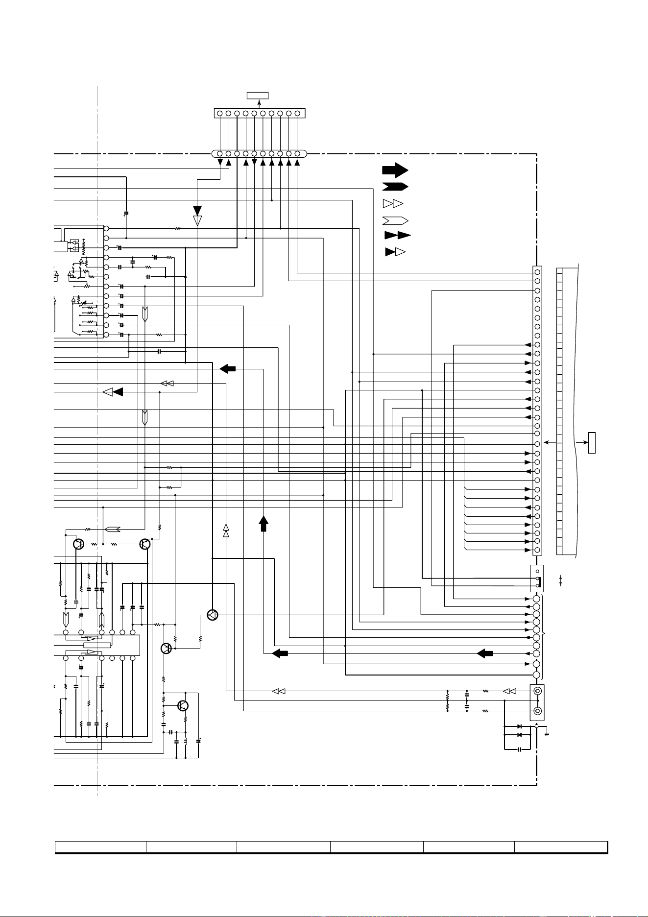
Figure 20 SCHEMATIC DIAGRAM (1/11)
A
B
C
D
E
F
G
H
1
23456
• NOTES ON SCHEMATIC DIAGRAM can be found on page 39.
R620
22K
9
10 11
1415161718192021222324
8
7
6
5
4
321
9
10
11
12
13
14
15
16
17
18
19
20
21
22
23
24
8
7
6
5
4
3
2
1
–15V
VF1
VF2
–VP
UN_SW_5V
P_IN
M_+12V
A+10V
GND
GND
L-CH
R-CH
SW_5V
GND
GND
GND
REC
_
SP_RLY
SP_DET
(A_+B) SW_5V
CD_+B SW_5V
A_+B
A_GND
L
L
R
R
P22 1 - F, G
TO POWER SECTION
P29 12 - D
TO CD SERVO PWB
CNP7
CD_+B
CD_GND
L-CH
A_GND
R-CH
T1_R
T1_L
A_GND
M_GND
ERASE
T2_R2
T2_R1
T2_L1
T2_L2
4
2
ERASE HEAD
TAPE 2
RECORD/
PLAYBACK HEAD
TAPE 1
PLAYBACK HEAD
R-CHL-CH
R-CH
L-CH
3
2
1
1
3
5
6
3
2
1
6
5
4
3
2
1
6
5
4
3
2
1
1
2
3
4
5
6
7
1
2
3
4
5
6
CD
TUNER
DECK
AUX
DI
CE
VSS
LOUT
LBASS
LTRE
LIN
L4
L3
L2
L1
CLK
VDD
VREF
ROUT
RBASS
RTRE
RIN
RSEL0
R4
R3
R2
R1
CCB
INTERFACE
+
–
+
–
+
–
+
–
+
–
+
–
+
–
+
–
LSEL0
ALC
ALC
RIPPLE
NOR/CRO2
–
–
+
–
+
Hich=T1
+
–
+
Hich=CHROME
56K
112K
56K
112K
2
1
3
2
1
3
1
2
3
4
5
6
7
8
9
10
11
12
13
14
15
17
18
19
20
21
MAIN PWB-A1(1/3)
+B
+B
+B
+B
+B
+B
+B
+B
+B
+B
+B
-B
-B -B
Q112~Q114: SWITCHING
Q101~Q106: SWITCHING
MU
T
MUTING
BI601
CNS601
CNP101
BI102
CNS102
Q104
2SC1845 F
C104
180P
R106
3.3K
R104
2.2K
Q102
2SC1845 F
R108
47K
R110
4.7K
Q106
KTC3199 GR
C106
560P
R112 15K
R116
56
C112
100/25
C114
0.033
R122
33K
C116
560P
C118
47/25
R124
5.6K
R120
3.9K
R118
100K
C120
0.0022
R126
3.9K
C121
0.022
C122
3.3/50
R128
6.8K
C124
270P
R132
100
C126
22/50
C132
47/25
C130
0.0033
C128
0.022
R130
1.5K
R134
10K
C108
330P
R114
1K
C110
330P
C107
330P
R113
1K
C109
330P
IC101
AN7345K
PLAYBACK AND RECORD/
PLAYBACK AMP.
C103
180P
Q103
2SC1845 F
R105
3.3K
R103
2.2K
Q101
2SC1845 F
C102
560P
C101
560P
C136
0.022
Q112
KTA1266 GR
R146
10K
R148
4.7K
R147
10K
Q113
KRC104 M
C141
100/16
C150
10/50
R149
150
C639
1/50
R621
22K
R618
330
R619
330
R604
10K
C610
1/50
C608
0.1
R606
3.9K
C612
0.0027
C606
0.15
C614
1/50
C616
4.7/50
C618
1/50
C620
1/50
C624
1/50
C622
1/50
R608
1.2K
C626
0.0056
R602
1K
R601
1K
IC601
LC75341
AUDIO PROCESSOR
C623
1/50
C
6
1/
5
C6
1/
5
C6
1/
5
C
6
4.7
/
C
6
1/
5
C60
5
0.15
C
0
C6
0
22/
5
Q
1
KTC3
1
R138
10K
R137
220K
R139
10K
C119
0.0022
R121
33K
R125
68K
R127
3.9K
R117
100K
C113
0.033
C111
100/25
R115
56
C115
560P
R119
3.9K
C117
47/25
R123
5.6K
C123
270P
R129
6.8K
C125
22/50
C127
0.022
R131
1.5K
R133
100
C129
0.0033
C131
47/25
R135
10K
C133
22/50
C134
220/10
C601
220/16
R614
3.3K
R615
3.3K
R613
390
R611
2.2K
C635
0.001
C636
0.001
R610
2.2K
R612
390
Q602
KTC3199 GR
Q601
KTC3199 GR
Q114
KRC104 M
R111
15K
R101
1K
R102
1K
R107
47K
C105
560P
Q105
KTC3199 GR
R109
4.7K
Q107
KTC3199 GR
R617
2.2K
R616
2.2K
C637
0.001
C638
0.001
Q604
KTC3199 GR
Q603
KTC3199 GR
C640
22/50
– 21 –
CD-BK250W/CD-BK2600W/CD-BK270W
Figure 21 SCHEMATIC DIAGRAM (2/11)
7
8 9 10 11 12
22
23
24
25
26
27
28
29
30
31
KOK OUT(L)
KOK IN(L)
KOK OUT(R)
KOK IN(R)
DI
CLK
KOK LATCH
MIC IN
A_GND
A_+10V
+B
9
10 11 12
131415161718
8
7
13
14
15
16
17
18
19
20
21
22
23
24
TUN_SM
DO
CE
A+10V
TUN_L
TUN_R
DI
CLK
REC_R
P27 12 - C
TO DISPLAY PWB
CNS701
(D_GND)GND
(A_GND)GND
P_IN
P25 11 - H
TO TUNER SECTION
–20dB
M_GND
SP_DET
UN_SW 5V
A_GND
SW_5V
D_GND
–15V
M_+12V
SP_RLY
VF2
–VF
VF1
SPA_SIG
SMUTE
REC/PLAY
T_T1/T2
T_BIAS
CLK
DI
TUN_SM
CE
DO
CHASSIS
R-CH
L-CH
9
1
12
10
11
17
18
19
20
21
22
23
24
25
26
27
28
29
30
31
32
32
16
15
14
13
1
4
2
3
8
7
6
5
CD
TUNER
DECK
AUX
CLK
VDD
VREF
ROUT
RBASS
RTRE
RIN
RSEL0
R4
R3
R2
R1
CCB
TERFACE
+
–
+
–
+
+
–
+
–
+
–
+
–
VCC
ALC
GND
ALC
RIPPLE
NOR/CRO2
–
+
–
+
Hich=CHROME
56K
56K
2
1
3
CD SIGNAL
MIC SIGNAL
VIDEO SIGNAL
RECORD SIGNAL
PLAYBACK SIGNAL
FM SIGNAL
+B
+B
+B +B
+B
+B
+B
+B
+B
+B
+B
-B
-B
+B
+B
1 2 3 4 5 6 7 8 9
10
1 2 3 4 5 6 7 8 9
10
CNPK1
P30 6 - C
TO MIC PWB
10 kHz/100 kHz
9 kHz/50 kHz
MUTING
MUTING
BIAS
SWITCHING
BIAS
0
.
0022
R126
3.9K
3
.
3/50
R128
6.8K
C124
270P
R132
100
C126
22/50
C132
47/25
C130
0.0033
C128
0.022
R130
1.5K
R134
10K
IC101
AN7345K
1
5
K
D
RECORD/
K
AMP.
C150
10/50
IC601
L
C75341
PROCESSOR
C623
1/50
C625
0.0056
R609
1.2K
C621
1/50
C619
1/50
C617
1/50
C615
4.7/50
C613
1/50
C605
0.15
C611
0.0027
R607
3.9K
C607
0.1
C603
22/50
C609
1/50
R605
10K
R623
220K
R622
220K
R136
220K
Q108
KTC3199 GR
R138
10K
R137
220K
R139
10K
68K
R127
3.9K
C123
270P
R129
6.8K
C125
22/50
C127
0.022
R131
1.5K
R133
100
C129
0.0033
C131
47/25
R135
10K
C133
22/50
C134
220/10
C135
0.022
R158
220
Q109
KTA1266 GR
R140
47K
R142
82
R143
47K
R144
22K
C137
0.047
(ML)
C138
0.0082
(PP)
C139
0.039(ML)
L103
330µH
R145
4.7
Q111
KTC3203 Y
C693
0.001
D691
DS1SS133
D690
DS1SS133
JK690
VIDEO/AUX
IN
R690
6.8K
R691
6.8K
C691
390P
C690
390P
R692
33K
CNP701
FFC701
BIK1
CNSK1
C601
220/16
R603
1K
R141
4.7K
Q110
KRC104 M
Q107
KTC3199 GR
C140
47/25
R693
33K
SW601
SPAN SELECTOR
CD-BK250W/CD-BK2600W/CD-BK270W
– 22 –
A
B
C
D
E
F
G
H
1
23456
• NOTES ON SCHEMATIC DIAGRAM can be found on page 39.
Figure 22 SCHEMATIC DIAGRAM (3/11)
+B2
2
1
3
1
2
3
3
2
1
3
2
1
–15V
M_+12V
P_IN
GND(CD_GND)
R-CH
L-CH
A+10V
GND(D_GND)
GND(A_GND)
GND(M_GND)
VF1
VF2
–VP
SP_RLY
SP_DET
SW_5V
CD_+B
A_+B
GND(A_GND)
P20 1 - C, D
TO MAIN SECTION
8
9
6
5
4
3
2
7
1
10
1
7
2
3
4
5
6
9
8
10
15
14
13
121110
9
8
7
6
5
4 3 2
1
CH1
OUT
OUT
CH2
CH2
CH1
–
–
+
+
+VCC
–VCC
R-CH
L-CH
1
2
4
3
6
20
7
9
17
18
19
13
8
21
5
14
10
12
11
IC901
STK4029S
POWER AMP.
R934
1K
C938
820P
C936
15P
R930
100K
C932
0.001
R932
56K
C930
0.22/50
R938
56K
R936
820
C934
4.7/50
R940
1K
R948
0.22
(2W)
R946
0.22
(2W)
C942
0.22
R942
22K
C940
100/50
R944
100
R950
0.1(1W)
R952
1K
C948
0.022
R954
1.5K
Q902
KTC3199 GR
D912
DS1SS133
C946
10/50
C945
10/50
C941
100/50
R945
0.22(2W)
R943
100
R935
1K
R941
1K
C937
15P
C939
820P
R939
56K
R937
820
C935
4.7/50
R947
0.22(2W)
Q904
KTC3199 GR R956
56K
R955
56K
C952
0.047
(ML)
R958
4.7
C953
0.047
(ML)
R959
4.7
R988
R986
R981
R982
D914
DS1SS13
3
R949
0.1(1W)
C947
0.022
Q903
KTC3199 GR
R951
1K
R953
1.5K
Q905
KTC3199 GR
D911
DS1SS133
R931
100K
C931
0.22/50
R933
56K
C915
0.022
C916
22/50
R909
22K
ZD904
DZ130BSB
ZD905
DZ2.4BSB
R908
560
IC902
KTC2026
C920
47/25
IC903
KIA7810AP
IC903
KIA7810AP
VOLTAGE
REGULATOR
C918
0.1
(ML)
C907
2200/35
C970
6800/16
C921
0.1
(ML)
D916
DS1SS133
C923
47/25
C904
2200/63
C903
2200/63
R902
22K
R903
3.3K
CNS902
BI902
Q914
KTC3199
R901
22K
C949
47/50
Q908
KRA107 M
C969
3.3/50
Q907
KRC107 M
C933
0.001
D913
DS1SS133
IC904
KIA7805AP
IC904
KIA7805AP
CONSTANT VOLTAGE REGULATOR
R957
56K
D917
DS1N404S
+B
+B
+B
+B
+B
+B
+B
+B
+B
+B
+B
+B
+B
+B
+B
+B
-B
-B
-B
– 23 –
CD-BK250W/CD-BK2600W/CD-BK270W
Figure 23 SCHEMATIC DIAGRAM (4/11)
7
8 9 10 11 12
B
2
TRANSFORMER
PWB-A3
MAIN PWB-A1 (2/3)
POWER PWB-A2
CD-BK270W ONLY
+
R1_OUT
L1_OUT
SP_RCH_GND
SP_LCH_GND
SP_RCH
SP_LCH
R-CH
L-CH
5
1
8
9
6
5
4
3
2
7
1
10
1
2
3
4
5
6
7
8
9
10
M
22
1 1
1
7
2
3
4
5
6
9
8
10
T.F.
220 V
127 V
110 V
230-240 V
AC POWER
SUPPLY CORD
AC 110/127/220/230-240 V
50/60 Hz
C952
0.047
(ML)
R958
4.7
R988 680
R986 680
R981 680
R982 680
R968
4.7K
R967
4.7K
RL914
RELAY
D914
DS1SS133
C967
47/50
R970
1K
Q906
KTC3203 Y
CNP971
FW981
BI903
CNS903
CNR1
D901
TS6B04GM
C901
0.1
(ML)
D905
DS1N404S
D903
DS1N404S
D902
DS1N404S
D904
DS1N404S
R984
47K
F901
T4A L 250V
F902
T4A L 250V
C902
0.1
(ML)
F904
T2A L 250V
F903
T2A L 250V
C908
100/50
D907
DS1N404S
C909
100/50
D906
DS1N404S
D908
DS1N404S
R905
47K
C911
47/50
R904
2.2K
Q901
KTA1274 Y
R906
10
C910
220/50
ZD901
DZ330BSB
ZD903
DZ6.2BSA
R977
47
R978
47
R907
12K
C913
100/35
C912
47/50
C905
0.1
(ML)
C906
0.1
(ML)
CNS971
R971
68K
D915
DS1SS133
C968
10/50
R972
15K
R983
220K
CNP902
CNS902
BI902
Q914
KTC3199 GR
R973
47K
ZD902
DZ110BSB
L920
L921
R969
4.7
PT801
POWER
TRANSFORMER
SO901
SPEAKER
TERMINAL
M901
FAN MOTOR
SW801
VOLTAGE SELECTOR
LUG1
LUG2
SR1
SURROUND
SPEAKER TERMINAL
HEADPHONES
PWB-B2
SURROUND
SPEAKER PWB-G2
1
2
3
4
5
CNP981
JK701
HEADPHONES
C734
220P
CR1
22/50
CR2
22/50
C735
220P
FM SIGNAL
+B
+B
+B
+B
+B
1
2
3
CD-BK250W/CD-BK2600W: 6 ohms
CD-BK270W: 8 ohms
1
2
3
1
2
3
CD-BK250W/CD-BK2600W/CD-BK270W
– 24 –
Figure 24 SCHEMATIC DIAGRAM (5/11)
A
B
C
D
E
F
G
H
1
23456
• NOTES ON SCHEMATIC DIAGRAM can be found on page 39.
AM BAND
COVERAGE fL
AM ANT.
FM SIGNAL
AM SIGNAL
1
1
2
2
3
2
1
9
8
7
6
5
4321
22
21
20
19
1
8
654321
24 23 22 21
3
2
1
VSS
AOUT
AIN
PD
DO
CL
DI
CE
X IN
X OUT
REG
AM RF IN
AM OSC IN
FM AFC
AM OSC OUT
AM MIX OUT
FM IF IN
1
3
2
MAIN PWB-A1(3/3)
+B
+B
AM
ANTENNA
BUFF
C301
0.01
CT1
0.01
C340
0.001
C330
15P
C331
0.047
C303
10P(CH)
BF301
BAND PASS FILTER
R372 1K
IC302
R365
10K
R302
10
C318
100P
R316
4.7K
R325
47K
R309
10K
C384
0.001
T302
FM IF
C305
4.7P
(CH)
C314
0.0047
R313
33K
R381
10K
X352
4.5 MHz
C363 0 022
T351
AM IF
C317
0.001
R311
100K
L312 FM RF
C332
0.022
C315
0.0047
C304
0.01
R314
22
C324
3.9P(UJ)
D305
DS1SS133
R378 1K
R327
33
CF303
VD302
SVC211C
VD303
SVC211C
T306
AM
OSC.
C338 0.001
D301 DS1SS133
D302 DS1SS133
C361 0.022
C362 3.3/50
VD301
SVC348S
R382
150
IC301
C397
0.022
C382
15P(CH)
R323
68K
R322
680
R375
470
C334
22P
(CH)
C335
560P
C380
10/50
C323
0.022
T303
AM TRACKING fL
C393
1/50
R380
1.5K
T301 FM OSC.
R373 1K
R374 1K
CNP301
C306
0.022
C307
10/50
C310
15P(CH)
Q302
KTC3194 Y
C309
0.001
C392
0.001
C394
47/25
C308 4.7P(CH)
C316
0.022
C352 10/50
C389 0.022
C312
0.022
R351 5.6K
C350 0.022
C313
22P
R358
3.9K
C342
0.022
C311
18P
C381
12P(CH)
R336
10K
TP301
IC301
TA7358AP
FM FRONT END
SO302
FM ANTENNA
TERMINAL
– 25 –
CD-BK250W/CD-BK2600W/CD-BK270W
Figure 25 SCHEMATIC DIAGRAM (6/11)
7
8 9 10 11 12
1
2
3
P21 12 - F
TO MAIN PWB
22
21
20
19
18
17
16
15
14
13
12
1110
987654321
24 23 22 21 20
19 18 17 16 15 14 13
121110
98
7
6
5
4
3
2
1
GND(D_GND)
GND(A_GND)
TUN_SM
DI
DO
CE
TUN_R
CLK
TUN_L
A+10V
IF
CONT
FM/AM
FM/AM
SD
MO/ST
ST IND
MO/ST
VSS
AOUT
AIN
PD
VDD
FM IN
AM IN
DO
CL
DI
CE
X IN
X OUT
IF IN
REG
AM IF IN
GND
SD
STEREO
FM DET
VCC
IF OUT
PHASE
(FM/AM)
PHASE
L-CH OUT
R-CH OUT
MPX IN
MPX VCO
FM/AM OUT
VSM
AM LOW CUT
AM RF IN
AM OSC IN
FM AFC
AM OSC OUT
AM MIX OUT
FM IF IN
30 24 22 27 29 26 24 23 25 31
+B
+B
+B
Q360: SWITCHING
R372 1K
IC302
IC302
LC72131
PLL(TUNER)
C364 2.2/50
IC303
LA1832S
FM IF DET./FM MPX./AM IF
R365
10K
R387
5.6K
C370
1/50
R393
1K
R376
1K
R355
3.3K
R359
1.8K
4
1
C369
27P
C374 0.015
ZD351
DZ5.1BSB
C396
100/10
C395
0.022
R381
10K
X352
4.5 MHz
R363
12K
C363 0.022
R391
270
Q360
KTA1266 GR
R385
5.6K
R392
270
C372
1/50
R364
12K
T351
AM IF
R361
15K
C355
22P
R388
3.9K
C371
1/50
R362
15K
R378 1K
R386
22K
C388
0.001
R356
1K
C368
1/50
C398
100/10
C356
0.001
C357
2.2/50
C358
1/50
CF352
R352
1K
C361 0.022
C362 3.3/50
R
382
150
C353 0.022
C399
0.022
C373
0.015
X351
456 kHz
C397
0.022
8
2
C
H)
C366 0.001
R350
2.7K
R357
470K
R383
5.6K
C391
47/25
R384
5.6K
R375
470
R395
47K
C386
330P
R360
4.7K
R377
47K
L351
100µH
C385
0.01
C380
10/50
R379
2.2K
C393
1/50
R380
1.5K
R373 1K
R374 1K
C387
0.022
C392
0.001
C394
47/25
C352 10/50
C389 0.022
R351 5.6K
C350 0.022
R358
3.9K
4
2
2
2
C365 0.022
C367
1/50
R353
270
CF351
C354 0.022
()
TP302
TP
CD-BK250W/CD-BK2600W/CD-BK270W
– 26 –
Figure 26 SCHEMATIC DIAGRAM (7/11)
A
B
C
D
E
F
G
H
1
23456
• NOTES ON SCHEMATIC DIAGRAM can be found on page 39.
M12V
P22
P21
P20
P19
P18
P17
P16
P15
P14
P13
P12
P11
P10
F
F
F
49
48
47
44
43
42 41
40
39
38
37 36
35
34 33 32
P09
P08
P07
P06
P05
P04
P03
P02
P01
G08
G09
G10
G11
31 30 29 28 27 26 25 24 23 16 15 14 13
9
93
92
91
90
89
88
87
86
85
8483
82
81
80
79
78
77
76
75
74
73
72
71
70
P1
P2
P3
P4
P5
P11
P12
P13
P14
G11
G10
G9
G8
P6
P7
P8
P9
P10
VLOAD
P15
P16
P17
P18
P19/DIST0
69
68
67
66
65
64
63
62
61
60
59
58
57
56
LCK 0
KARAOKE LATCH
FPB
MIC SW
NO USE / MPEG_POW
DISTOUT/SW OUT
RDS-READY/ESS_DO
RDS-RDCL/ESS_DI
RDS-RDDA/ESS_STB
RDS-RST/ESS_ACK
P22/DIST3
P21/DIST2
P20/DIST1
NO USE
REMOCON
VSS
SMUTE
T_SOL_A
T_MOTOR
T_SOL_B
JOG 0
44 43 42 41 40 39 38
TIMER LED
VDD
AC RLY_CONT
SPK
_
DET
SP
_
RLY
50 49 48 47 46 45
55
54
53
52
51
PLAY SW_B
CD CLAMP
SW
T2
RUN
FPA
T1
RUN
NO USE
8
7
6
5
4
3
2
1
8
7
6
5
4
3
2
1
T2 PLAY
T2 RUN
+MTR
SOL2
SOL1
T1 RUN
GND
F_REC
R_REC
4
5
1
6
3
2
7
8
9
10
+B
+B
+B
+B
+
+B
+B
+B
+B
+B
+B
+B
+B
+B
+B
+B
+B
+B
+B
-B
-B
-B
-B
1
10
+
-
M
TAPE MECHANISM
PWB-D
9
10
8
7
6
5
4
3
2
1
TAPE
MOTOR
PLAY
F. PLAY
CASSETTE
SOLENOID
SOLENOID
PH
FFC702
CNS702
D701
DS1SS133
D705
DS1SS133
R770
10K
R772
10K
C706
47/50
R724
1K
R726
2.2K
R727
2.2K
R728
2.2K
R729
1K
R732
1K
R733
1K
R734
1K
LED701
R761
10K
IC701
IX0427AW
SYSTEM
MICROCOMP
U
R572
100K
C572
0.022
ZD561
DZ6.2BSB
C573
0.022
C569
2.2/50
R578
100K
R731
10K
R778
10K
R779
10K
R777
10K
Q708
KTA1271 Y
Q707
KTA1271 Y
Q706
KTA1273 Y
C712
47/50
D709
DS1SS133
D710
DS1SS133
R756
10K
R758
10K
R759
10K
R760
10K
R755
1K
R752
33
R579
15K
C571
0.022
C566
2.2/50
R747
1K
R746
1K
R748
1K
R749
100K
R750
100K
R751
100K
R571
390K
D563
DS1SS133
D562
DS1SS133
R580
180K
IC562
KIA4558P
OPE AMP.
C567
0.0068
D561 DS1SS133
R573
56K
R568
220K
R566
220K
R565
33K
R567
68K
R563
270
R562
820K
R574
1M
R576
2.2M
R561
10K
C568
0.0068
C561
270P
R570
12K
C565
0.0027
R738
22K
R739
1K
R740
1K
R741
1K
R569
100K
C570
0.022
R575
470K
C707
1/50
D716
DS1SS133
FL701
FL DISPLAY
R735
1K
R736
1K
C564
0.0027
C562
270P
IC561
KIA4558P
OPE AMP.
Q701
KTC3199 GR
Q702
KTC3199 GR
Q703
KTC3199 GR
C563
2.2/50
R577
150K
DISPLAY PWB-B1
R754
10K
R753
1K
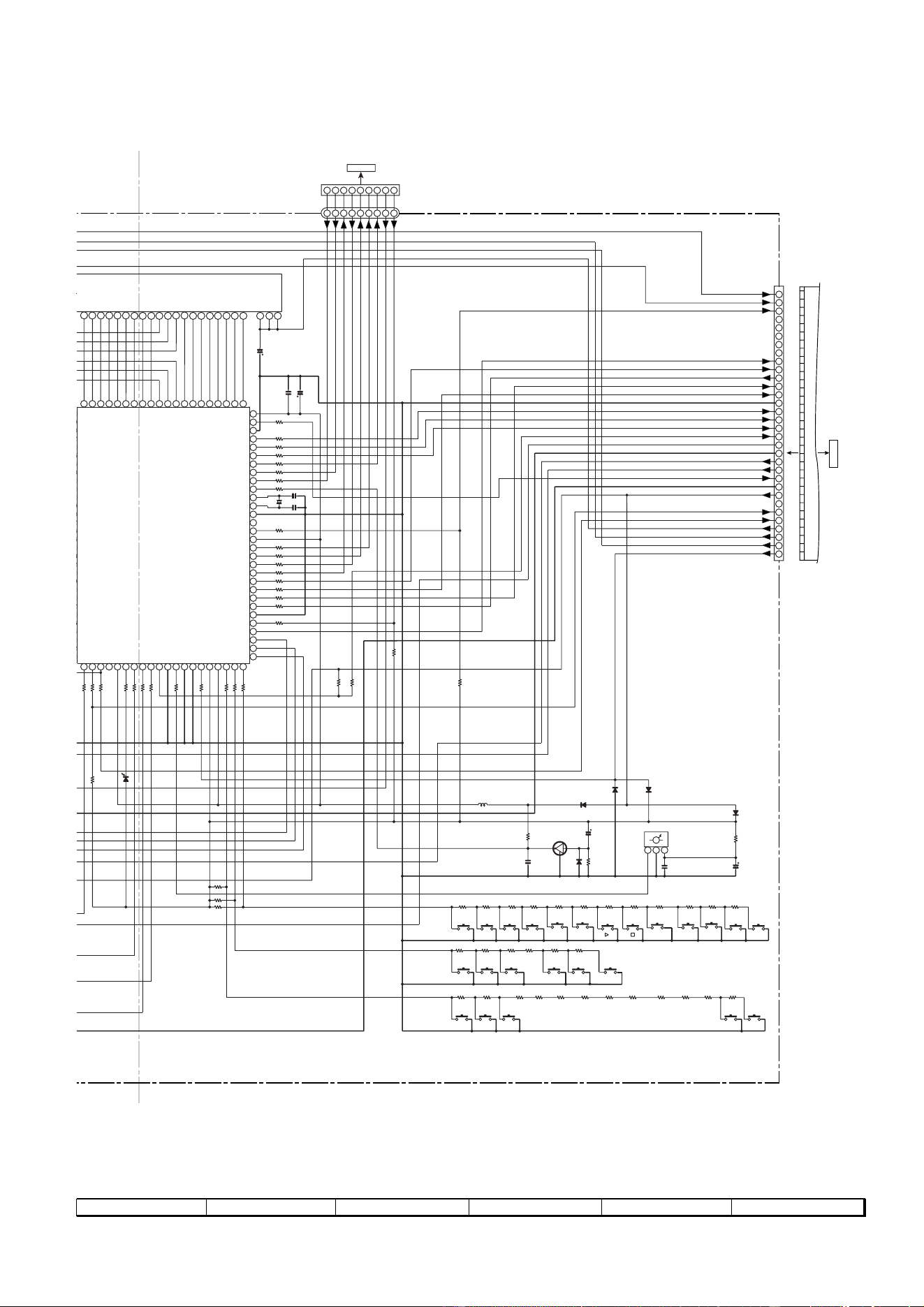
– 27 –
CD-BK250W/CD-BK2600W/CD-BK270W
Figure 27 SCHEMATIC DIAGRAM (8/11)
7
8 9 10 11 12
5V BACK UP
2
1
3
P09
P08
P07
P06
P05
P04
P03
P02
P01
G01
G02
G03
G04
G05
G06
G07
G08
G09
G10
G11
F
F
F
31 30 29 28 27 26 25 24 23 16 15 14 13 12 11 10
9876
321
DISC_NO SW
WRQ(DSP)
CLAMP SW
CD DO
CD DI
CD CE
CD CLK
DRF
RES OUT
P29 12 - B
TO CD SERVO PWB
123456789
123456789
100
99
98
97
96
95
9493
92
91
90
89
88
87
86
85
8483
82
81
0
9
8
7
6
5
4
3
2
0
11
10
9
8
7
6
5
4
3
2
1
T-BIAS
T_T1/T2
X2
RESET
WRQ
P1
P2
P3
P4
P5
P11
P12
P13
P14
DSA_STB
REC/PLAY
RES OUT
G11
G10
G9
G8
G7
G6
G5
G4
G3
G2
G1
VDD
-20dB
DRF
P6
P7
P8
P9
VLOAD
P15
P16
P17
P18
P19/DIST0
9
8
7
6
5
4
3
2
0
9
8
7
6
LCK 0
KARAOKE LATCH
FPB
MIC SW
NO USE / MPEG_POW
DISTOUT/SW OUT
RDS-READY/ESS_DO
RDS-RDCL/ESS_DI
RDS-RDDA/ESS_STB
RDS-RST/ESS_ACK
P22/DIST3
P21/DIST2
P20/DIST1
NO USE
25
24
23
22
21
20
19
18
17
16
15
14
13
12
VDD
X1
CD CE
CD DI
SPAN
CE
Vpp/IC
CD CLK
CD DO
CLK
DI
DO
AVSS
XT2
P-IN
VF1
VF2
–VP
SMUTE
SP_RLY
A_GND
–15V
SW_5V
UN_SW 5V
SP_DET
M_GND
SPA_SIG
–20dB
M_+12V
22
20
21
13
14
15
17
23
24
32
19
16
18
30
28
29
25
31
32
27
26
11
12
10
D_GND
REC/PLAY
T_T1/T2
T_BIAS
DI
CE
CLK
DO
TUN SM
SPAN
KARAOKE LATCH
MIC IN
ESS_STB
ESS_ACK
ESS_DQ
ESS_DI
SW OUT
1
1
2
3
4
9
8
7
6
5
30
29
28
27
26
O/C SW/
DSA DATA
TUN SM
DSA_ACK
SPEANA2
AVDD
KEY 2
KEY 1
KEY 0
P_IN
REMOCON
VSS
SMUTE
T_SOL_A
T_MOTOR
T_SOL_B
AVref
JOG 0
JOG 1
44 43 42 41 40 39 38 37 36 35 34 33 32 31
TIMER LED
VDD
AC RLY_CONT
SPK
_
DET
SP
_
RLY
50 49 48 47 46 45
5
4
3
2
PLAY SW_B
CD CLAMP
SW
FPA
N
NO USE
321
CNP701
P21 12 - D
TO MAIN PWB
FFC701
+B
+B
+B
+B+B
+B
+B
+B
+B
+B
+B
+B
+B
+B
+B
+B
+B
+B
+B
+B
+B
+B
-B
+B
+B
+B
+B
+B
+B
+B
+B
+B
-B-B
-B
RESET
R725
1K
R771
10K
CNS701
RD07
3.9K
RD06
2.7K
RD05
2.2K
RD04
1.5K
RD03
1K
RD30
5.6K
RD16
3.9K
SW717
VOLUME
UP
SW718
VOLUME
DOWN
SW719
REVERSE
MODE
RD17
180K
D711
DS1SS133
R774
10K
R773 1K
D713
DS1SS133
C714
3.3/50
R782
100K
D715
DS1SS133
Q709
KRC102 M
C702
220/10
C703
0.022
C701
1/50
R781
47K
C715
0.01
R765
4.7K
R718
1K
R719
1K
R720
1K
R721
1K
R724
1K
R726
2.2K
R727
2.2K
R728
2.2K
R729
1K
R732
1K
R733
1K
34
K
LED701
R761
10K
IC701
IX0427AW
SYSTEM
MICROCOMPUTER
D712
DS1SS133
L701
100µH
D714
DS1SS133
C716
0.022
RX701
REMOTE
SENSOR
R766
10K
R768
10K
R767
10K
BI701
CNP8
CNS8
R783
100
C717
47/50
SW727
STOP
RD01
680
SW701
ON/
STAND-BY
RD02
820
SW702
CLOCK
SW703
TIMER
RD09
10K
RD08
5.6K
SW732
TUNER
RD29
100K
SW731
VIDEO
RD28
33K
SW730
TUNING
UP
RD27
18K
SW716
EQUALIZER
RD14
820
SW715
X-BASS
RD13
680
SW725
FAST
FORWARD
RD21
1.5K
SW726
PLAY
RD23
2.7K
SW723
MEMORY/
SET
RD26
10K
SW724
FAST
REWIND
RD25
5.6K
RD22
2.2K
RD24
3.9K
SW712
DISC
SKIP
RD10
18K
RD12
100K
SW713
OPEN/
CLOSE
RD11
33K
RD15
1.8K
L
AY
C705
18P
R710 1K
R711 1K
R712 1K
R713 1K
R714 1K
R715 1K
R716 1K
R707 1K
R702 1K
R703 1K
R717 1K
R706 1K
SW729
REC/
PAUSE
SW728
REVERSE
PLAY
RD20
1K
RD19
820
RD18
680
SW720
CD
SW721
TAPE
SW722
TUNING
DOWN
SW714
DIMMER
R705 1K
R708 1K
R704 1K
R709 1K
R769 1K
XL700
4.194304 MHz
C704
15P
SPEANA0
SPEANA1
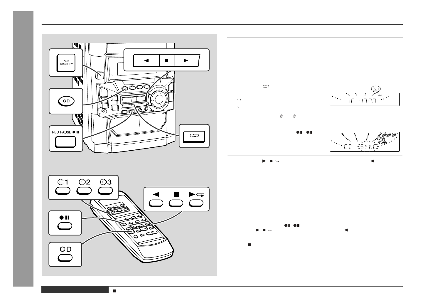
CD-BK250W/CD-BK2600W/CD-BK270W
– 28 –
A
B
C
D
E
F
G
H
1
23456
• NOTES ON SCHEMATIC DIAGRAM can be found on page 39.
Figure 28 SCHEMATIC DIAGRAM (9/11)
CD SIGNAL
CD MOTOR PWB-F
CD SERVO PWB-C
4
1
9
101112131415161718192021
22 23 24 25 26 27 28 29 30 31 32 33 34 35 36 37 38 39 40 41 42
8
7
6
5
4321
9
10
11
12
13
14
15
16
17
18
19
20
212
2
807
9
8
7
6
5
4
3
2
1
TP3
TP2
TP1
LD_
M
LD_M–
VCC4
M–
M+
VCC3
SPO
VCC2
SLDO
VCC
STANDBY
VREF
MUTE
TO
FD
SP–
SL–
SL+
SP+
TR–
TR+
FO+
FO–
GND
GND
GND
FO–
FO–
LD
VR
PD
FO+
TR+
TR–
C
F
B
A
E
GND
PUIN
SL+
SL–
SP–
SP+
VREF
VCC
PICKUP UNIT
TR–
LDD
LDS
S
PD
O
FDO
TDO
REFI
VRE
F
ADAV
S
ADAV
JITT
C
RFM
O
TE
TEC
FE
TIN2
TIN1
FIN2
FIN1
RSV
S
RFV
D
RF
EFM
I
SLCI
SLCO
TR–
TR+
TR+
FO+
FO+
FO–
PD
VR
LD
F
C
B
A
E
VCC
VREF
+
+
–
–
1
2
3
4
5
6
1
2
3
4
5
6
5
3
6
2
7
1
4
5
3
6
2
7
1
4
5
3
6
2
7
1
4
5
3
6
2
7
1
4
4
1
3
6
5
2
4
1
3
6
5
2
M
M
4
8
5
2
1
7
3
6
4
8
5
2
1
7
3
6
4
8
5
2
1
7
3
6
4
8
5
2
1
7
3
6
+
+
–
–
+
–
+
+
–
–
+
–
+
–
+
–
2
LASER DRIVER
CNP1
CNS1A
CNS1B
R6
33K
R5
12K
R4
12K
R3
33K
R1
12K
R2
12K
C1
47/25
C2
0.01
CNP2
CNS2A
CNS2B
C38
0.01
C39
100/10
R44
12K
C41
100/10
CNP3
CNS3A
CNS3B
R13
1K
R14
1K
R15
1K
C12
100P
C11
0.22/50
C10
10/50
C9
100/10
C50
22P
(CH)
R12
330
R65
3.3K
C7
100P
R10
27K
C5
0.047(ML)
R11
10K
R9
3.3
Q1
KTA1266 GR
C4
0.001
C49
47/25
C3
47/25
R42
1.2K
C8
0.0047
C6
0.1
IC2
M63001FP
FOCUS/TRACKING/
SPIN/SLED DRIVER
C40
220/6.3
R7
47
M1
SPINDLE
MOTOR
M2
SLED
MOTOR
SW4
PICKUP IN
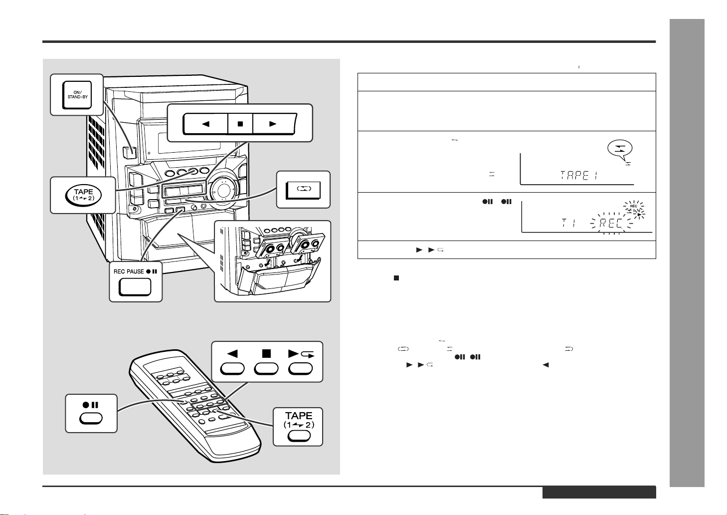
– 29 –
CD-BK250W/CD-BK2600W/CD-BK270W
Figure 29 SCHEMATIC DIAGRAM (10/11)
7
8 9 10 11 12
• The numbers 1 to 12 are waveform numbers shown in page 40.
CD RES
O/C, DISC NO
CLAMP SW
P27 9 - A
FROM DISPLAY PWB
CL
DI
DO
CE
DRF
WRQ
P20 1 - B
FROM MAIN PWB
8
3
5
7
12
11
10
9
6
4
1
37 38 39 40 41 42
6
5
4321
9
10
11
12
13
14
15
16
17
18
19
20
2122 2324 2526 2728 2930 3132 3334 3536 3738 3940
8079 7877 7675 7473 7271 7069 6867 6665 6463 6261
41
42
43
44
45
46
47
48
49
50
51
52
53
55
56
57
58
59
60
54
8
7
6
5
4
3
2
1
TP2
TP1
LD_M+
LD_M–
VCC4
M–
M+
TO
FD
TR
+
FO+
FO–
M
+5V
LDD
LDS
FR
VVDD
PCKIST
VVSS
PDO2
PDO1
CONT2
CONT3
VSS
VDD5
DRF
*RES
*WRQ
DO
DI
CL
CE
DATA
DATACK
LRSY
ASDFIN
ASDACK
ASLRCK
16MOUT
EFLG
C2F
XVSS
FSX/16MIN
XIN
XOUT
XVDD
RVDD
RCHO
RVSS
LVSS
LCHO
LVDD
TEST
DOUT
VDD
VSS
MONI5
MONI4
MONI3
MONI2
MONI1
FSEQ
V/*P
DEFECT
SBCK/FG
CONT5
CONT4
GPDAC
SLDO
SPDO
FDO
TDO
REFI
VREF
ADAVSS
ADAVDD
JITTC
RFMON
TE
TEC
FE
TIN2 F
TIN1 E
FIN2 B
FIN1 A
RSVSS
RFVDD
RF
EFMIN
SLCIST
SLCO
+5V
DGND
L-CH
AGND
R-CH
6
3
5
4
2
6
1
3
5
4
2
6
1
3
5
4
2
6
1
9
8
7
6
2
4
5
3
1
5
4
3
2
1
3
1
2
CNS8
CNS601
CD LOADING
MOTOR PWB-E
2
Q2: CONSTANT VOLTAGE
/
10
R49
1
D2
DS1SS133
D1
DS1SS133
Q3
KRC102 M
R45
470
R46
470
R20
10K
R13
1K
R14
1K
R15
1K
R16
1K
R18
1K
R17
1K
C12
100P
C11
0.22/50
C10
10/50
C
9
0
/10
0
P
H
)
R12
330
7
0
P
C5
0.047(ML)
R11
10K
C33
100P
C32
100P
C30
100P
C28
100P
C27
0.022
R42
1.2K
R41 12K
C37
0.1
C36
2.2/50
R40
680
R31
1K
R29
2.2K
R28
2.2K
R22
100
C51
0.022
L1
0.82µH
C24
10/50
R25
2.2K
R27
10K
ZD1 DZ3.3BSB
C13
0.022
R26
10K
C25
0.0015
C23
10/50
C44
0.001
R24
2.2K
C16
330/6.3
C48
0.022
R23
220
ZD2
DZ3.9BSB
R30
8.2K
R19
15K
CNP4
CNS4
BI4
CNP8
IC1
LC78645E
CD SERVO
R47
100
R80
3.3
C18
100/10
Q2
KTC3203 Y
C26
0.0015
C14
100/10
R32 1K
R37 1K
R36 1K
R35 1K
R34 1K
R33 1K
R38 1K
C8
0.0047
R39
680
C35
0.047
(ML)
C
6
.1
C34
100P
CNP7
M3 T/T
UP DOWN
LOADING
SW1
OPEN/CLOSE
SW2
CLAMP
SW3
DISC NO.
R43
220
XL1
33.8688 MHz
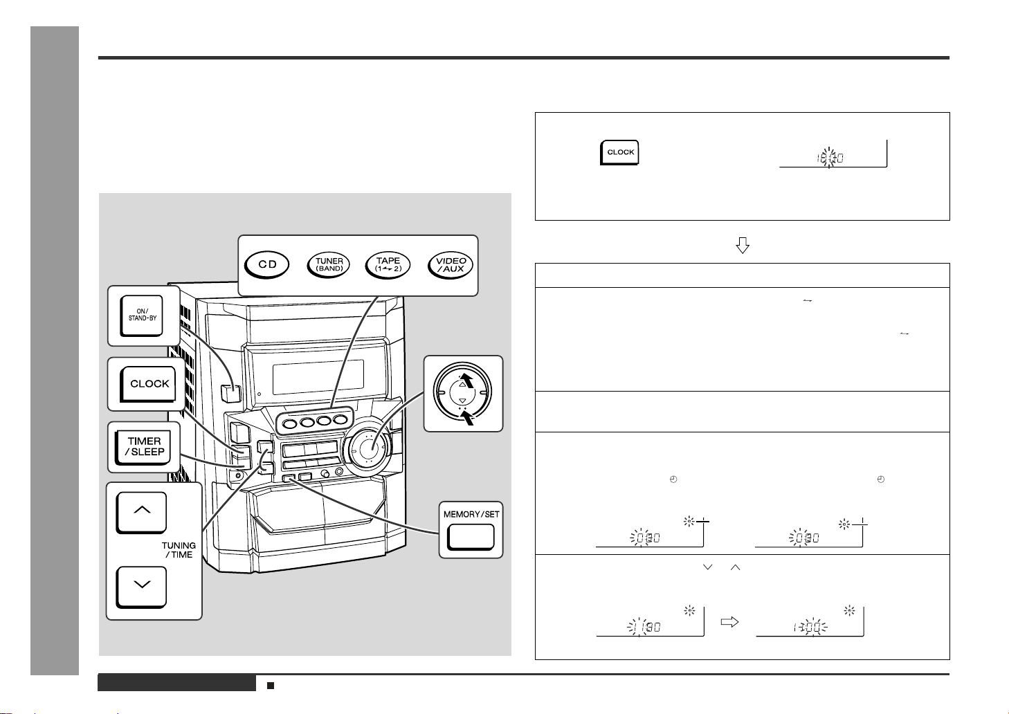
CD-BK250W/CD-BK2600W/CD-BK270W
– 30 –
A
B
C
D
E
F
G
H
1
23456
Figure 30 SCHEMATIC DIAGRAM (11/11)
Figure 30 WIRING SIDE OF P.W.BOARD (1/8)
• NOTES ON SCHEMATIC DIAGRAM can be found on page 39.
1
2
3
4
5
6
7
8
9
10
MICSW
DATA
CLOCK
LATCH
PS2
PS1
VCF IL
L OUT
R OUT
SOURCEOUT
KEYCONIN
R IN
L IN
VOL IN
LPF2OUT
LPF2IN2
LPF2IN1
DAINTOUT
DAINTIN
DACONT
VCC
GND
MCLKCONT
VACL
MIC1 IN
ALC1
ALC2
MIC1NF IN
MIC2NF IN
MIC1 OUT
MIC2 OUT
MIC1VOL IN
MIC2VOL IN
MICOUT
LPF1 IN1
LPF2 IN2
LPF1 OUT
AD INTIN
ADCONT
REF
AD INTOUT
MIC2 IN
MIC SIGNAL
42
41
40
39
38
37
36
35
34
33
32
31
30
29
28
27
26
25
24
23
22
12
11
10
9
8
7
6
5
4
3
2
1
21
20
19
18
17
16
15
14
13
8
7
6
5
4
3
2
1
MIC I
DATA
CLOCK
MIC LATCH
MIC IN(R)
MIC OUT(R)
A_+10V
A_GND
MIC IN(L)
MIC OUT(L)
CHASSIS
GND
ICK2
KIA4558P
MIC PWB-G1
CNSK1
FROM
MAIN PWB
P21 8-A
RK40
1k
RK37
390
RK39
1k
CK2
0.47
CK6 0.1
CK41
100/16
CK10 0.1
CK11 0.1
CK7 0.47
CK44
47/25
CK72
100/16
RK42 10K
VRK1
20K(B)
MIC
VOLUME
CK53
47/50
RK48
10K
RK50
10K
CK47
220P
RK43
18K
CK48 220P
RK46
18K
CK45
2.2/50
CK46
2.2/50
RK49
10K
RK41 10K
CK51
1/50
CK52
1/50
RK47
8.2K
RK45
6.8K
RK44
6.8K
CK49
100P
CK50
100P
RK5
1K
CNPK1
CK42
0.022
RK38
100
RK14
100
RK15
100
RK36
390
CK19
0.022
RK8 5.6K
CK23 0.001
CK1 0.01
RK11 1K
RK10 1K
RK9 1K
CK43
47/25
ZDK1
MTZJ5.6B
RK12
100
RK13
1.2K
QK1
KTC3203Y
ICK1
M65856SP
MIC AMP.
RK2 56K
RK3
56K
RK4 10K
RK7
1K
JK1
MIC
CK9 2.2/50
CK8 4.7/50
CK13
0.0047
CK17 220/10
CK16 0.22
CK15 0.068
CK25 2.2/50
CK26 2.2/50
CK12
2.2/50
CK14 0.001
CK21 0.068
CK24 2.2/50
CK33 47P
CK30 2.2/50
CK29 2.2/50
CK31 0.15
CK35 47P
CK34 47P
CK22 0.0047
CK20 0.22
DK1
DS1SS133
PINK1
DK2
DS1SS133
RK1
10K
ICK2
KIA4558P
OPE PMP.
1
2
3
4
5
6
7
8
9
10
B
C
E
1
2
3
4
8
7
6
5
123456789
10111213141516171819
2021
424140393837363534333231302928272625242322
MIC PWB-G1
CK29
PINK1
CK3
DK2
DK1
CK31
CK35
CK34
RK11
RK10
RK9
RK13
RK12
QK1
ZDK1
RK15
RK14
CNPK1
CNSK1
FROM MAIN PWB
RK40
RK38
RK36
RK37
CK72
RK39
RK46
CK45
RK41
RK42
CK46
CK47
RK43
CK48
CK50
RK47
RK45
CK49
ICK2
RK49
CK51
RK44
RK48
RK50
CK52
CK53
CK44
CK43
CK41
CK10
CK1
RK4
RK5
RK8
RK7
CK9
CK11
CK13
CK15
CK8
CK14
CK12
RK3
RK1
CK2
CK6
CK7
CK16
RK2
CK17
ICK1
CK33
CK20
CK42
CK19
CK30
CK26
CK25CK24
CK21
CK22
JK1
MIC
CK23
VRK1
MIC VOLUME
P33 7 - A
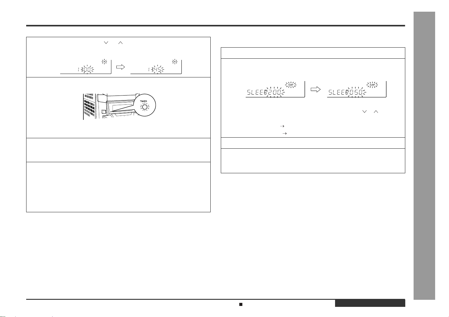
– 31 –
CD-BK250W/CD-BK2600W/CD-BK270W
Figure 31 WIRING SIDE OF P.W.BOARD (2/8)
7
8 9 10 11 12
C902
CNP902
CNS902
P33 11 - F
FROM MAIN PWB
D901
R984
R983
D903
D904
D905
D902
C906
C905
C908
ZD902
D906
C901
C909
C911
R904
D908
F904
T2A L 250V
F903
T2A L 250V
F901
T4A L 250V
F902
T4A L 250V
R978
R977
D907
ZD903
ZD901
C913
R905
R907
R906
C912
Q901
C910
T.F
PT801
POWER TRANSFORMER
AC POWER
SUPPLY CORD
AC 110/127/220/230-240 V
50/60 Hz
POWER PWB-A2
TRANSFORMER PWB-A3
1
BC E
2345678910
230-240 V
110 V
127 V
LUG1
LUG2
220 V
SW801
VOLTAGE SELECTOR
230-240 V
220 V
127 V
110 V
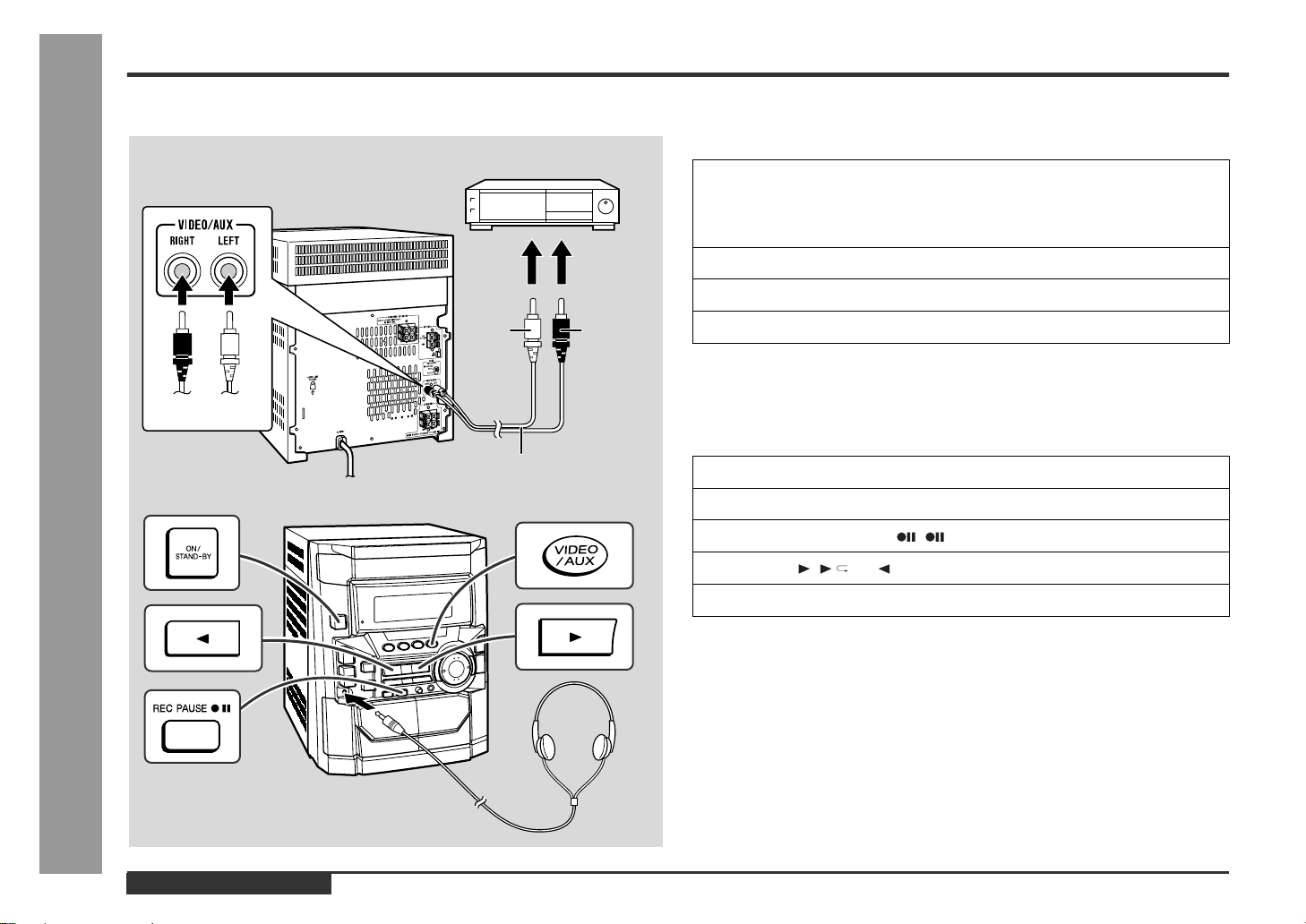
CD-BK250W/CD-BK2600W/CD-BK270W
– 32 –
Figure 32 WIRING SIDE OF P.W.BOARD (3/8)
A
B
C
D
E
F
G
H
1
23456
SO901
SPEAKER
TERMINAL
SR1
SURROUND
SPEAKER
TERMINAL
ZD351
C370
C610
C358
R60
2
C371
C373
C374
R601
C372
R618
R616
D912
R952
Q902
C948
R954
C949
R930
C930
C
C934
R903
C91
R944
R908
C942
R902
R901
C952
R950
R946
C903
R958
RL914
D914
R948
R947
R945
R949
R959
C953
IC901
LG1
R968
C940
C941
R943
R935
C946
C945
R973
Q914
C931
C935
C640
C967
R969
D911
Q905
Q904
Q903
D913
Q907
Q908
C969
R619
Q602
Q604
C639
Q601
T306
C365
C364
C368
R357
R358
C362
C367
VD302
IC303
X351
D305
L312
CF303
C357
C350
T302
R309
CF351
C352
VD303
Q302
C398
T301
T351
CF352
R382
C393
R375
Q360
C380
C394
L351
C391
IC302
R384
R387
R386
C396
X352
C307
1
2
3
4
5
6
7
8
9
IC301
R314
CNP301
D301
D302
BF301
132
CT1
T303
C331
D690
D691
Q906
Q603
R970
C968
R971
R972
D915
R967
L920
L921
VD301
IC
9
CNP971
123456789
10 11 12
24 23 22 21 20 19 18 17 16 15 14 13
123456789
10 11
22 21 20 19 18 17 16 15 14 13 12
123456789
101112131415
1
2
1
1
1
1
2
3
3
2
3
2
JK690
VIDEO AUX IN
R-CH
L-CH
AM LOOP
ANTENNA
1
2
SW601
SPAN
SELECTOR
9 kHz/50 kHz
10 kHz/100 kHz
SO302
FM
ANTENNA
TERMINAL
FM
75 OHMS
GND
B
C
E
B
C
E
E
BCE
ECB
1
2
3
3
2
1
C
B
B
B
B
C
E
CE
1
1
2
3
23
C
E
B
C
E
E
C
B
EC B
BC E
B
C
C395
R395
C388
C356
R355
C355
R363
R361
R364
R362
R604
R932
C932
R936
R942
R938
C936
R934
C938
R956
R940
R955
R941
C939
C637
C937
R939
R617
R620
R937
C933
C638
R933
R957
R931
R951
C947
R953
C636
R610
R614
R612
R621
R611
C635
R615
R605
R613
C335
C332
R323
R356
C363
C342
R350
C334
C361
R336
R365
TP301
TP302
C369
R316
C316
R313
C366
R311
C308
C309
C399
C389
R351
C353
R352
C354
R353
C312
C310
C313
C311
R302
R327
C324
R325
R322
R383
R380
R381
R393
C385
C318
R385
R377
C392
R379
C387
C386
R360
C381
R359
R376
C382
R388
R374
R372
R373
R378
C384
C301
C397
C306
C304
C305
C315
C303
C314
C317
C323
C330
C338
C340
C693
R691
C691
R693
C690
R690
R692
R392
R391
1
2
CNS971
RD
BR
M901
FAN MOTOR
R-CH
L-CH
BL
SURROUN SPEAKER PWB-G2
R-CH
L-CH
R-CH
L-CH
CNR1
BI903
CNS903
CR2
CR1
BR
WH
CD-BK270W ONLY
CD-BK250W/CDBK2600W: 6 ohms
CD-BK270W: 8 ohms
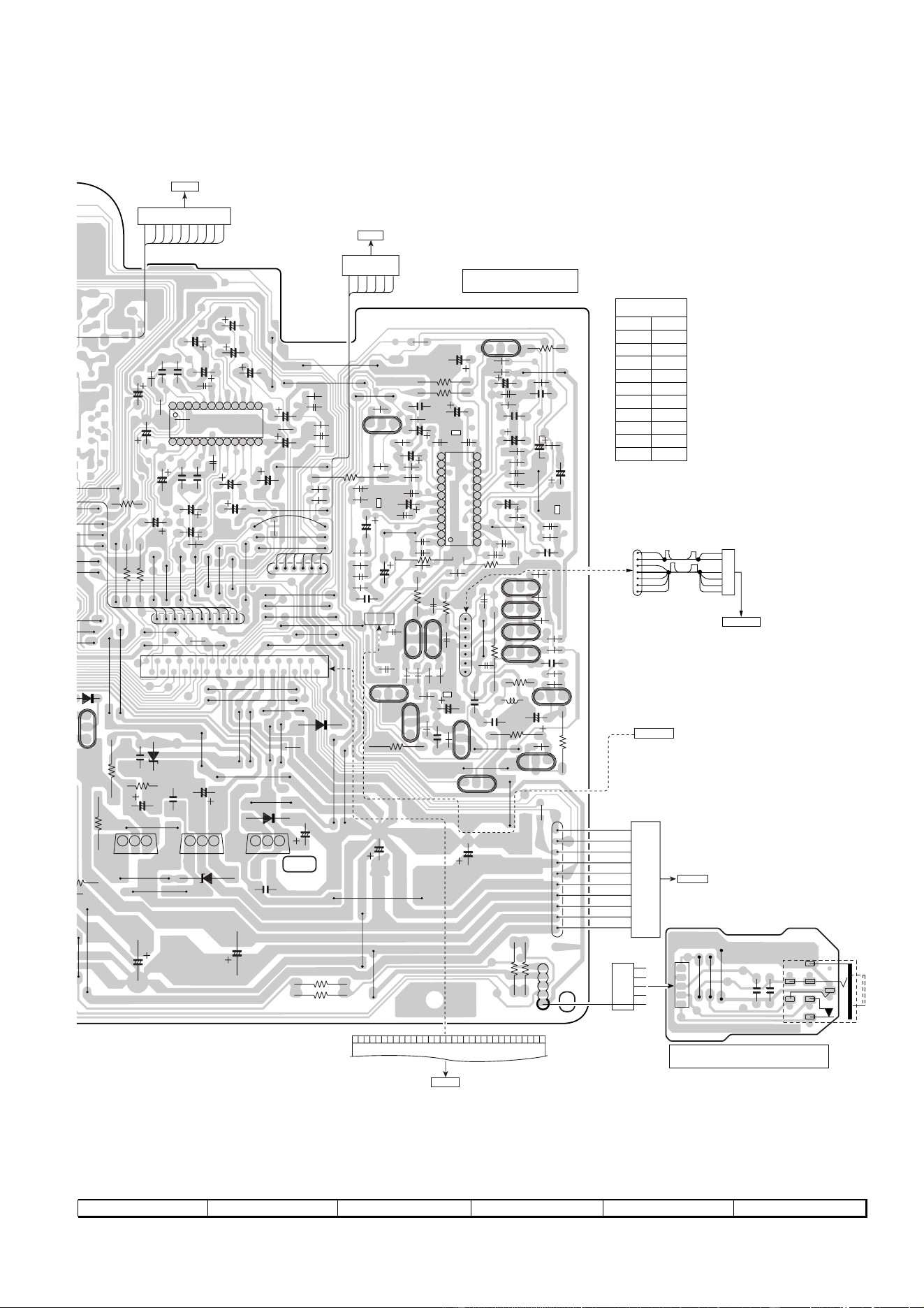
– 33 –
CD-BK250W/CD-BK2600W/CD-BK270W
Figure 33 WIRING SIDE OF P.W.BOARD (4/8)
7
8 9 10 11 12
WH
WH
BK
PK
WH
GR
BL
BK
PK
BK
WH
YL
BL
BI102
7
1
2
3
4
5
6
1
CNS102
TO TAPE 2 RECORD/
PLAYBACK HEAD
P37 12 - E
R137
Q107
C134
C131
C119
C133
C127
C150
C125
IC101
C122
R115
R114
Q104
R113
Q102
CNP101
Q105
Q106
Q101
BI102
R112
Q103
C137
R145
C138
Q114
Q111
L103
C141
Q113
C140
C139
Q112
C136
R142
R141
R149
Q109
Q110
C970
BI902
1
10
R988
R981
R986
R982
C904
C921
ZD905
C907
C923
D916
D917
C920
C918
CNP701
BIK1
FFC701
CNS701
P35 12 - A
TO DISPLAY PWB
C114
BI601
CNS601
CNSK1
CNP7
1
6
C112
C615
C118
C613
C619
C617
C621
R136
C605
C607
C623
IC601
C624
C614
C622
C606
C618
C616
C620
C608
C610
C601
C603
R602
C609
R603
2468
10
12 14 16 18 20 22 24
32
1
1
10
1
3579
11
13 15 17 19 21 23 25 27 29 31
26 28 30 32
R601
D912
Q902
ZD904
C915
R903
R909
C916
R908
9
02
C903
FW981
1
5
IC904
IC903
IC902
123456789
10 11 12
24 23 22 21 20 19 18 17 16 15 14 13
1
2
3
4
5
6
7
8
9
10
11
12
24
23
22
21
20
19
18
17
16
15
14
13
321
7
1
GY
WH
GY
WH
GY
WH
GY
WH
GY
RD
10
9
8
7
6
5
4
3
2
1
CNP902
TO POWER PWB
GY
WH
GY
WH
GY
RD
123456
GY
WH
GY
WH
GY
RD
P36 5 - A
TO CD SERVO PWB
CNPK1
P30 5 - G
TO MIC PWB
FROM
TAPE 1
PLAYBACK HEAD
P37 10 - E
RD
GY
WH
GY
WH
GY
WH
GY
GY
WH
12345678910
P31 9 - H
BR
COLOR TABLE
RD(R)
OR
YL
GR
BL
VL
GY
WH(W)
BK
PK
BROWN
RED
ORANGE
YELLOW
GREEN
BLUE
VIOLET
GRAY
WHITE
BLACK
PINK
BCE
BCE
ECB
ECB
ECB
ECB
ECB
E
E
C
B
B
C
E
E
C
B
E
C
B
1
1
123123BCE
23
123
2
3
CB
R131
R135
R121
C129
R133
R134
C135
C130
R132
R123
R127
R129
R130
C123
R128
R125
C124
C121
R117
C115
R119
C108
C109
C110
C107
R102
R101
R106
C104
C106
R104
R103
C101
C105
R111
R105
C103
R107
R108
R109
R110
C102
R144
R143
R148
R147
R146
R140
R118
C116
R120
R124
R607
R122
R623
C120
R622
R126
C611
C625
R609
R138
C626
R608
C612
R606
C735
C734
JK701
HEADPHONES
CNP981
CNS902
1
2
3
4
5
HEADPHONES PWB-B2
MAIN PWB-A1
C113
C117
C111
R116
Q108
C132
C126
R158
R139
C128
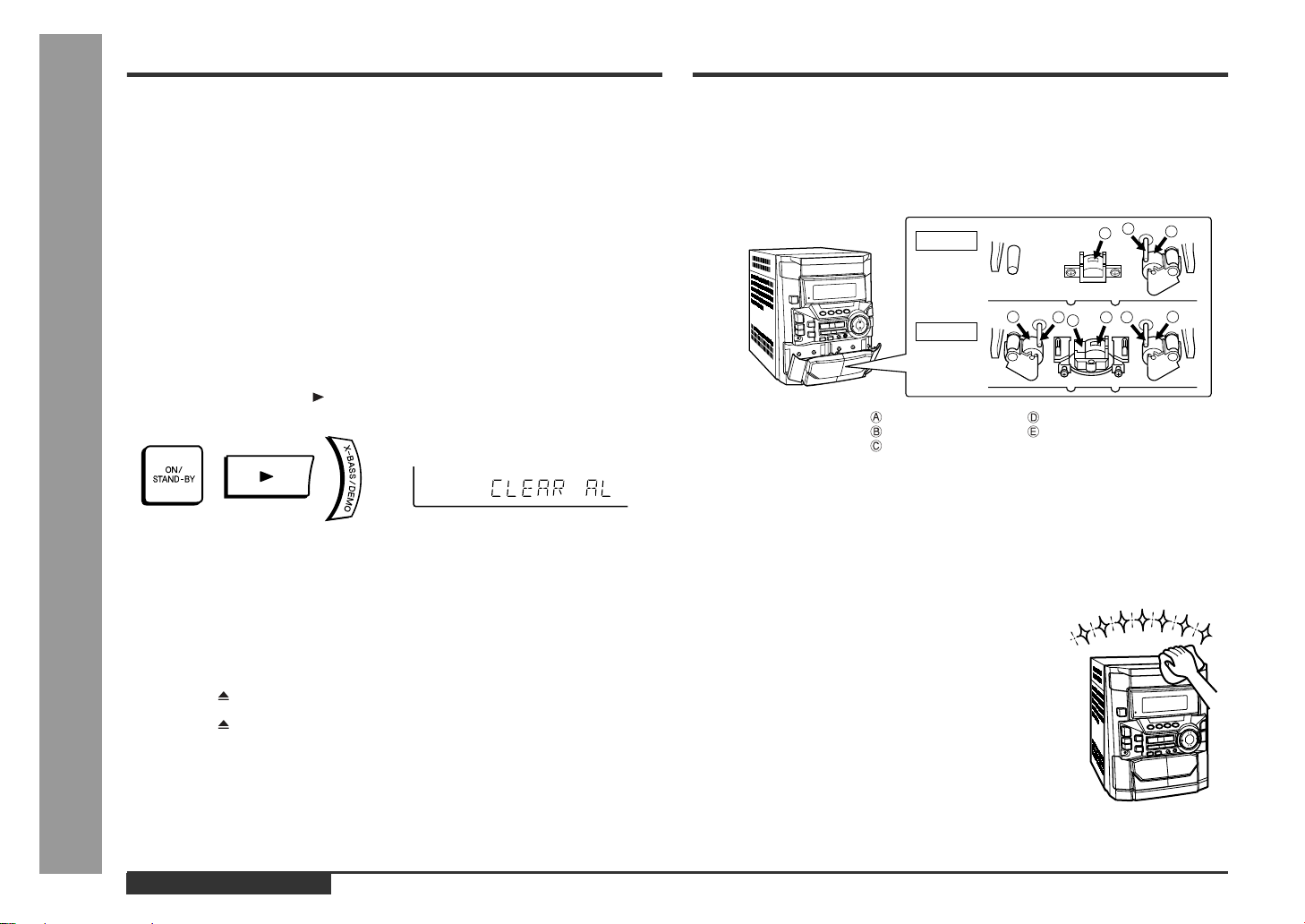
CD-BK250W/CD-BK2600W/CD-BK270W
– 34 –
Figure 34 WIRING SIDE OF P.W.BOARD (5/8)
A
B
C
D
E
F
G
H
1
23456
R702
R703
R704
X
L
F
SW718
VOLUME DOWN
D709
RD16
Q707
SW716
EQUALIZER
RD15
RD08
D711
SW717
VOLUME UP
SW731
VIDEO
R579
C563
D712
C714
D561
D715
C566
Q709
L701
C717
R708
Q701
Q702
Q703
BI701
CNP8
CNS8
P36 4 - A
TO CD SERVO PWB
1
9
C701
C702
RX701
R566
R570
IC561
D562
C561
D716
IC562
1
2
3
4
8
7
6
5
1
2
3
4
8
7
6
5
ZD561
D563
C573
SW713
OPEN/
CLOSE
R563
D714
D713
C569
Q706
SW715
X-BASS
Q708
D710
SW712
DISC
SKIP
C712
CNS702
FFC702
P37 9 - A
1
E
C
B
E
C
B
E
C
B
3
5
7
2468
9
10
10
9
8
7
6
5
4
3
2
1
1
DISPLAY PWB-B1
TO TAPE MECHANISM PWB
BR
COLOR TABLE
RD(R)
OR
YL
GR
BL
VL
GY
WH(W)
BK
PK
BROWN
RED
ORANGE
YELLOW
GREEN
BLUE
VIOLET
GRAY
WHITE
BLACK
PINK
WH
GY
WH
GY
WH
GY
WH
GY
RD
R
7
R
7
R
7
RD1
R778
R777
RD30
RD07
RD06
R569
R781
R782
R783
C715
R751
R750
R749
R748
R747
R746
R571
R568
C564
C565
R567
R565
C716
C562
R561
R562
R572
C572
C570
R577
C571
R580
C568
R576
R574
C567
R573
R575
R578
RD09
RD12
R779
RD11
RD10
1 2 3 6 7 8 9 10111213141516
B
1
2
3
C
E
B
C
E
B
C
E
321
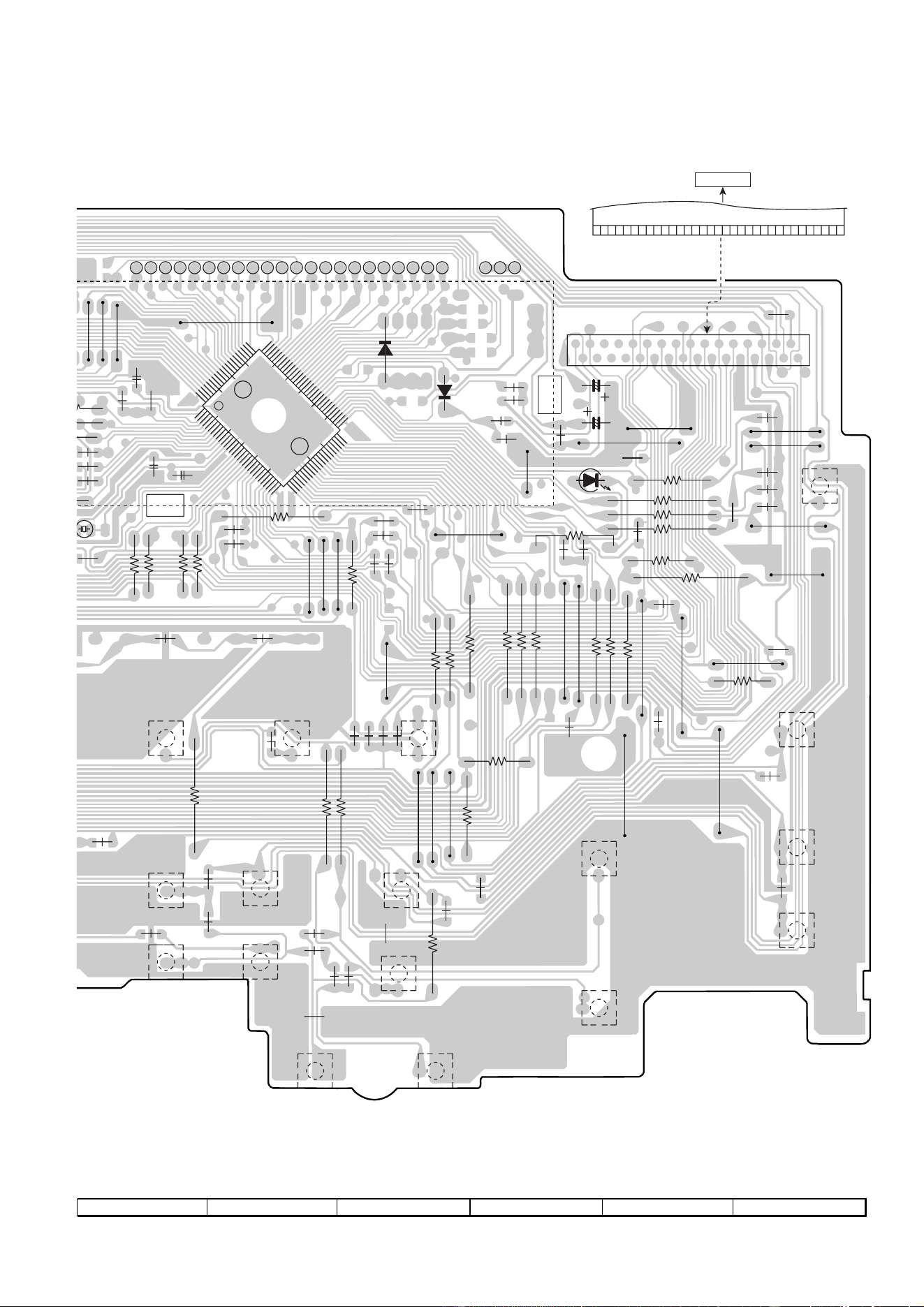
– 35 –
CD-BK250W/CD-BK2600W/CD-BK270W
Figure 35 WIRING SIDE OF P.W.BOARD (6/8)
7
8 9 10 11 12
R769
CNS701
CNP701
P33 9 -H
TO MAIN PWB
FFC701
SW701
ON/STAND-BY
R740
R739
R738
R736
R725
R765
R773
SW714
DIMMER
SW702
CLOCK
SW703
TIMER
SW723
MEMORY/SET
SW722
TUNING DOWN
SW724
FAST REWIND
RD26
SW728
REVERSE PLAY
SW730
TUNING UP
R770
R772
SW720
CD
R719
R720
R721
R735
R734
R724
R728
R727
R726
R718
R729
C706
C707
D701
D705
XL700
R712
R711
R710
R709
SW732
TUNER
SW721
TAPE
RD03
RD28
RD19
SW726
PLAY
SW725
FAST
FORWARD
SW729
REC/PAUSE
LED701
1357911131517192123
24681012141618202224
25 27 29 31
26 28 30 32
1
32
SW727
STOP
SW719
REVERSE MODE
R760
R756
R759
R758
R774
R771
R732
RD13
RD02
RD25
RD01
R767
R766
R768
RD18
R731
R713
R716
R761
R733
R717
R741
R755
R753
R754
R752
C703
R701
IC701
100
81
80
95
90
85
75
70
65
60
55
51
50
45
40
35
31
30
1
25
20
15
10
5
R705
C704
R706
C705
R707
R714
R715
RD04
RD05
RD29
RD14
RD24RD23
RD27
RD17
RD22
RD20
RD21
FL701
23 24 25 26 27 28 29 30 31 32 33 34 35 36 37 38 39 40 41 42 43 44 47 48 49
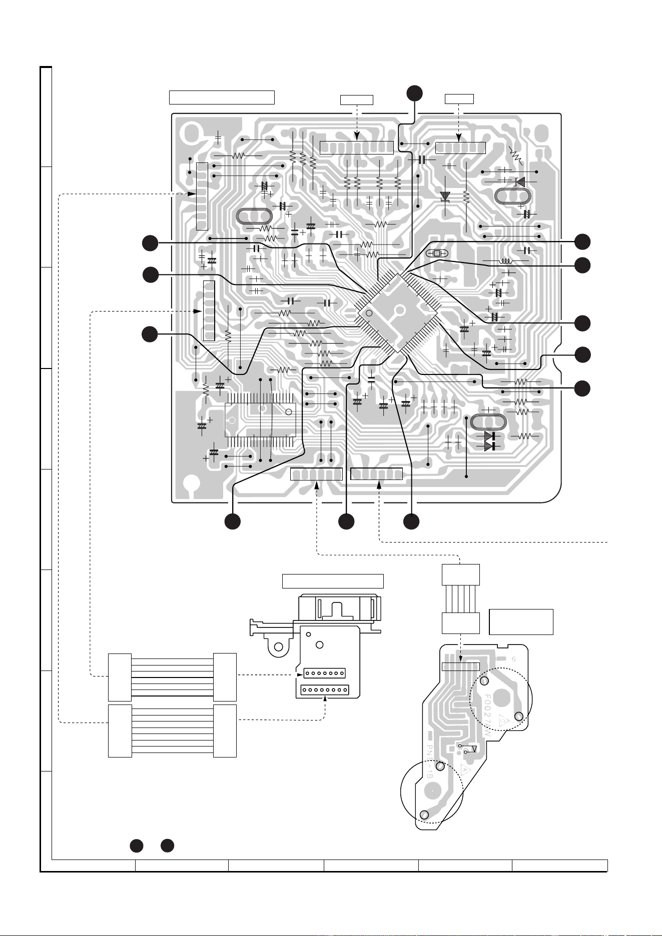
CD-BK250W/CD-BK2600W/CD-BK270W
– 36 –
Figure 36 WIRING SIDE OF P.W.BOARD (7/8)
A
B
C
D
E
F
G
H
1
23456
• The numbers 1 to 12 are waveform numbers shown in page 40.
4 2 1
5
7
8
6
9
10
11
12
3
12 3
R65
R19
R30
R18
R20
C23
D1
D2
Q3
C14
C16
C11
CNP4
C10
C12
C9
R3
R6
1
5101520
25 30 35 40
42
22
21
CNP3
R1
R4
R2
80
61
60
75
70
65
55
50
45
35
30
25
21
20
15
10
5
1
41
40
R5
R49
C39
C41
R44
C40
CNP1
CNP2
C1
R7
Q1
C5
R9
C49
R10
C3
R38
C37
C50
R37
C36
R36
C6
C35
R35
R34
CNP8
R29
R28
R33
R31
R32
C51
ZD1
R22
CNP7
C24
L1
Q2
ZD2
C48
C18
XL1
CD SERVO PWB-C
CNS703
P34 1 - C
FROM DISPLAY PWB
1
2
3
4
5
6
7
8
1
2
3
4
5
6
7
CNS1B
CNS1A
CNS2B
BL
WH
BL
WH
BL
WH
RD
RD
WH
GY
WH
GY
WH
GY
WH
1
2
3
4
5
6
7
8
1
2
3
4
5
6
7
8
1
2
3
4
5
6
7
3
4
1
2
5
6
7
17
1
8
PICKUP UNIT(306)
CNS3B
CNS3A
RD
WH
GR
WH
GR
WH
CD MOTOR
PWB-G
12345
6
12345
6
-
M1
SPINDLE MOTOR
SW4
PICKUP IN
M2
SLED MOTOR
+
-
+
12345
6
65
4
3
2165
4
3
21
CNS11
P33 9 - B
FROM MAIN PWB
12
3
4
56
12
3
4
567
89
ECB
BCE
C25
R26
R24
R17
C44
R45
R16
R46
C13
R15
R14
R13
IC1
IC2
C2
C38
C7
C8
R12
C4
R11
R42
R41
R40
R39
C32
C33
C34
C27
C30
C28
R43
C42
C26
R25
R47
R23
R27
R80
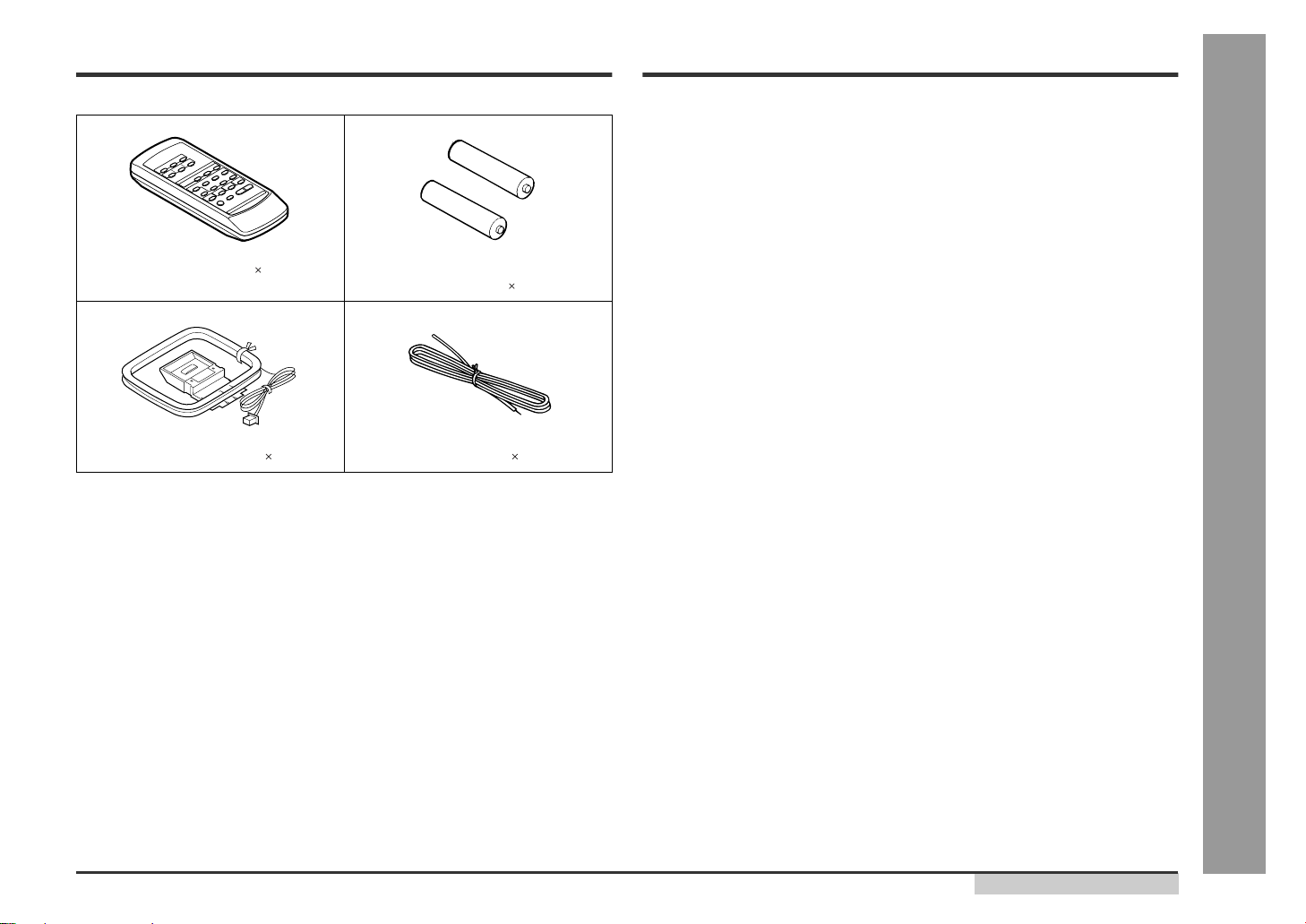
– 37 –
CD-BK250W/CD-BK2600W/CD-BK270W
Figure 37 WIRING SIDE OF P.W.BOARD (8/8)
7
8 9 10 11 12
654321
CNS102
TAPE 2
RECORD/PLAYBACK/ERASE HEAD
-
+
16
123
456
BI4
RD
WH
BK
WH
BK
WH
CNS4
SW3
DISC
NUMBER
CD LOADING MOTOR
PWB-E
M3
T/T UP/DOWN
MOTOR
SW2
CLAMP
SW1
OPEN/
CLOSE
–
+
CNP101
P33 11 - E
TO MAIN PWB
TAPE 1
PLAYBACK HEAD
PK
BK
BK
WH
WH
PK
GR
23
1
TAPE
MOTOR
1
1
2
3
2
4
5
6
79
810
1
10
CNS702
SOLENOID
PH
SW
SWSW
SW
SOLENOID
TAPE MECHANISM PWB-F
TAPE MECHANISM
ASSEMBLY
P34 4 - H
TO DISPLAY PWB
FFC702
BR
COLOR TABLE
RD(R)
OR
YL
GR
BL
VL
GY
WH(W)
BK
PK
BROWN
RED
ORANGE
YELLOW
GREEN
BLUE
VIOLET
GRAY
WHITE
BLACK
PINK
P33 11 - D
TO MAIN PWB
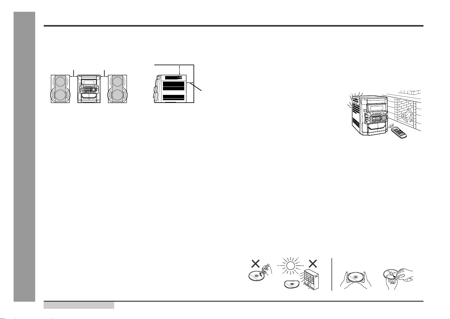
CD-BK250W/CD-BK2600W/CD-BK270W
– 38 –
VOLTAGE
1.6 V
1.0 V
1.6 V
1.8 V
3.3 V
0 V
1.6 V
1.6 V
1.6 V
1.6 V
1.6 V
1.6 V
1.5 V
1.5 V
1.5 V
1.5 V
0.8 V
3.2 V
0 V
1.6 V
1.6 V
1.6 V
1.6 V
0 V
0 V
3.2 V
0 V
0 V
0 V
0 V
0 V
0 V
0 V
0 V
1.6 V
0 V
0 V
3.2 V
3.2 V
0 V
9
8
7
6
5
4
3
2
1
30
29
28
27
26
25
24
23
22
21
20
19
18
17
16
15
14
13
12
11
10
40
39
38
37
36
35
34
33
32
31
PIN
NO.
VOLTAGE
IC1
3.7 V
3.7 V
0 V
0 V
3.7 V
3.2 V
3.2 V
3.2 V
0 V
0 V
0 V
3.2 V
0 V
0 V
0 V
0 V
0 V
3.2 V
0 V
0 V
0 V
4.7 V
0 V
4.9 V
4.9 V
4.9 V
0 V
4.9 V
0 V
0 V
0 V
0 V
0 V
0 V
0 V
3.2 V
3.2 V
3.2 V
0 V
3.2 V
PIN
NO.
VOLTAGE
41
54
53
55
56
57
58
59
60
61
62
63
64
65
66
67
68
69
70
52
51
50
49
48
47
46
45
44
43
42
75
74
76
77
78
79
80
73
72
71
4.77 V
4.68 V
0 V
0 V
4.67 V
4.72 V
4.74 V
0 V
5.41 V
4.86 V
2.3 V
2 V
0 V
4.76 V
0 V
4.77 V
4.7 V
0 V
5.36 V
0.16 V
0 V
0 V
0 V
0 V
0 V
2.3 V
0.22 V
0 V
0 V
0 V
5.03 V
5.03 V
5.03 V
4.77 V
5.04 V
2.48 V
0 V
0 V
4.92 V
0 V
5.67 V
12.5 V
12.52 V
12.5 V
3.8 V
4.78 V
4.76 V
4.5 V
5.04 V
5.28 V
9
8
7
6
5
4
3
2
1
30
29
28
27
26
25
24
23
22
21
20
19
18
17
16
15
14
13
12
11
10
40
39
38
37
36
35
34
33
32
31
PIN
NO.
VOLTAGE
IC701
5.28 V
0 V
0 V
5.25 V
5.28 V
5.28 V
0 V
0.31 V
0 V
0 V
0 V
0 V
0 V
0 V
0 V
0 V
–28.82 V
–28.82 V
–28.8 V
–28.88 V
–28.79 V
–28.8 V
–16.2 V
–18.74 V
–26.3 V
–23.77 V
0 V
–21.2 V
–28.9 V
–26.2 V
–26.3 V
–26.3 V
–21.26 V
–28.83 V
0 V
0 V
–18.73 V
0 V
0 V
–26.26 V
–26.26 V
–26.24 V
–26.32 V
–26.3 V
–26.29 V
–26.3 V
–26.3 V
–26.3 V
–26.28 V
–26.3 V
PIN
NO.
VOLTAGE
51
64
63
65
66
67
68
69
70
71
72
73
74
75
76
77
78
79
80
62
61
60
59
58
57
56
55
54
53
52
85
84
86
87
88
89
90
83
82
81
50
49
48
47
46
45
44
43
42
41
95
94
96
97
98
99
100
93
92
91
1.7 V
1.7 V
1.8 V
2.1 V
2.1 V
2.1 V
2.0 V
0 V
0 V
0 V
0 V
0 V
0 V
0 V
2.1 V
2.1 V
1.6 V
4.9 V
3.0 V
1.6 V
0 V
0 V
4.9 V
4.9 V
1.6 V
2.1 V
2.1 V
0 V
0 V
0 V
0 V
0 V
0 V
0 V
0 V
4.2 V
0 V
2.1 V
2.1 V
4.9 V
3.7 V
3.7 V
9
8
7
6
5
4
3
2
1
30
29
28
27
26
25
24
23
22
21
20
19
18
17
16
15
14
13
12
11
10
40
39
38
42
41
37
36
35
34
33
32
31
PIN
NO.
VOLTAGE
IC2
0.8 V
1.0 V
0.75 V
2.46 V
4.43 V
2.42 V
2.43 V
2.46 V
2.46 V
2.45 V
2.47 V
2.46 V
2.46 V
2.47 V
2.47 V
2.47 V
2.47 V
2.47 V
2.47 V
0.6 V
2.46 V
0 V
4.85 V
0.59 V
2.47 V
2.47 V
2.47 V
2.47 V
2.47 V
2.43 V
2.47 V
2.47 V
2.43 V
2.47 V
2.45 V
2.47 V
2.46 V
0 V
0 V
0 V
0 V
0 V
9
8
7
6
5
4
3
2
1
30
29
28
27
26
25
24
23
22
21
20
19
18
17
16
15
14
13
12
11
10
40
39
38
42
41
37
36
35
34
33
32
31
PIN
NO.
VOLTAGE
ICICK1
0 V
0 V
0 V
5.03 V
5.00 V
5.01 V
5.01 V
5.03 V
5.01 V
5.01 V
5.01 V
5.01 V
5.01 V
5.01 V
5.01 V
5.01 V
5.03 V
5.01 V
5.01 V
5.00 V
5.04 V
5.03 V
10.03 V
0 V
9
8
7
6
5
4
3
2
1
24
23
22
21
20
19
18
17
16
15
14
13
12
11
10
PIN
NO.
VOLTAGE
IC601
0 V
0 V
0.57 V
2.0 V
0.59 V(AC)
1.32 V
0 V
0.59 V
3.45 V
3.42 V
0 V
0 V
6.92 V
4.13 V
0 V
3.43 V
0.59 V
0 V
2.63 V
0.56 V(AC)
2.00 V
0.57 V
0 V
0 V
9
8
7
6
5
4
3
2
1
24
23
22
21
20
19
18
17
16
15
14
13
12
11
10
PIN
NO.
VOLTAGE
IC101
2.09 V
5.17 V
2.09 V
2.08 V
0 V
5.15 V
5.15 V
3.02 V
5.17 V
4.35 V
4.01 V
4.01 V
4.10 V
1.18 V
1.19 V
2.08 V
1.79 V
1.79 V
0 V
0.58 V
2.60 V
2.96 V
5.17 V
3.64 V
9
8
7
6
5
4
3
2
1
24
23
22
21
20
19
18
17
16
15
14
13
12
11
10
PIN
NO.
VOLTAGE
IC303
2.55 V
0 V
0 V
0 V
0 V
5.16 V
0 V
4.69 V
4.02 V
4.10 V
5.15 V
0 V
5.15 V
0 V
0 V
2.53 V
5.16 V
0.90 V
0.90 V
1.31 V
0 V
2.55 V
9
8
7
6
5
4
3
2
1
22
21
20
19
18
17
16
15
14
13
12
11
10
PIN
NO.
VOLTAGE
IC302
0 V
0 V
0 V
50.1 V
–48.8 V
0 V
0 V
51.6 V
–51.5 V
0 V
0 V
–50.1 V
0 V
0 V
0 V
9
8
7
6
5
4
3
2
1
15
14
13
12
11
10
PIN
NO.
VOLTAGE
IC901
0.17 V
0.2 V
0.19 V
–13.11 V
0.19 V
0.2 V
0.17 V
6.23 V
8
7
6
5
4
3
2
1
PIN
NO.
VOLTAGE
IC561
3
2
1
PIN
NO.
VOLTAGE
IC902
12.56 V
24.75 V
13.17 V
3
2
1
PIN
NO.
VOLTAGE
IC903
24.70 V
0 V
10.04 V
3
2
1
PIN
NO.
VOLTAGE
IC904
12.21 V
0.66 V
5.68 V
8
9
7
6
5
4
3
2
1
PIN
NO.
VOLTAGE
IC301
0.91 V
1.64 V
5.40 V
1.62 V
0 V
5.41 V
4.65 V
5.37 V
5.41 V
0.25 V
0.3 V
0.3 V
–13.11 V
0 V
0 V
0 V
6.23 V
8
7
6
5
4
3
2
1
PIN
NO.
VOLTAGE
IC562
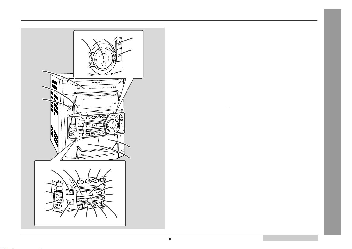
– 39 –
CD-BK250W/CD-BK2600W/CD-BK270W
• The indicated voltage in each section is the one measured
by Digital Multimeter between such a section and the chas-
sis with no signal given.
1. In the tuner section,
indicates AM
indicates FM stereo
2. In the main section, a tape is being played back.
3. In the deck section, a tape is being played back.
( ) indicates the record state.
4. In the power section, a tape is being played back.
5. In the CD section, the CD is stopped.
• Parts marked with “ 1 ” ( ) are important for
maintaining the safety of the set. Be sure to replace these
parts with specified ones for maintaining the safety and
performance of the set.
NOTES ON SCHEMATIC DIAGRAM
• Resistor:
To differentiate the units of resistors, such symbol as K and
M are used: the symbol K means 1000 ohm and the symbol
M means 1000 kohm and the resistor without any symbol is
ohm-type resistor. Besides, the one with “Fusible” is a fuse
type.
• Capacitor:
To indicate the unit of capacitor, a symbol P is used: this
symbol P means pico-farad and the unit of the capacitor
without such a symbol is microfarad. As to electrolytic
capacitor, the expression “capacitance/withstand voltage”
is used.
(CH), (TH), (RH), (UJ): Temperature compensation
(ML): Mylar type
(P.P.): Polypropylene type
• Schematic diagram and Wiring Side of P.W.Board for this
model are subject to change for improvement without prior
notice.
REF. NO
DESCRIPTION
POSITION
SW719 REVERSE MODE ON—OFF
SW720 CD ON—OFF
SW721 TAPE ON—OFF
SW722 TUNING DOWN ON—OFF
SW723 MEMORY/SET ON—OFF
SW724 REWIND ON—OFF
SW725 FAST FORWARD ON—OFF
SW726 PLAY ON—OFF
SW727 STOP ON—OFF
SW728 REVERSE PLAY ON—OFF
SW729 REC/PAUSE ON—OFF
SW730 TUNING UP ON—OFF
SW731 VIDEO/AUX ON—OFF
SW732 TUNER (BAND) ON—OFF
SW801 VOLTAGE SELECTOR 110 V—127 V—
220 V—230-240 V
SW1 OPEN/CLOSE ON—OFF
SW2 CLAMP ON—OFF
SW3 DISC NUMBER ON—OFF
SW4 PICKUP IN ON—OFF
SW601 SPAN SELECTOR 9/50 Hz—10/100 Hz
SW701 ON/STAND-BY ON—OFF
SW702 CLOCK ON—OFF
SW703 TIMER/SLEEP ON—OFF
SW712 DISC SKIP ON—OFF
SW713 OPEN/CLOSE ON—OFF
SW714 DIMMER ON—OFF
SW715 X-BASS/DEMO ON—OFF
SW716 EQUALIZER ON—OFF
SW717 VOLUME UP ON—OFF
SW718 VOLUME DOWN ON—OFF
TYPES OF TRANSISTOR AND LED
(1) (2) (3)
(S) (G) (D)
E C B
FRONT
VIEW
KTA1266 GR
KRC102 M
KRC104 M
KTA1271 Y
KTA1274 Y
2SC1845 F
KTA1273 Y
KTC3203 Y
KTC3199 GR
KRA107 M
KRC107 M
KTC3194 Y
SLR342VCJ1
FRONT
VIEW
REF. NO DESCRIPTION POSITION
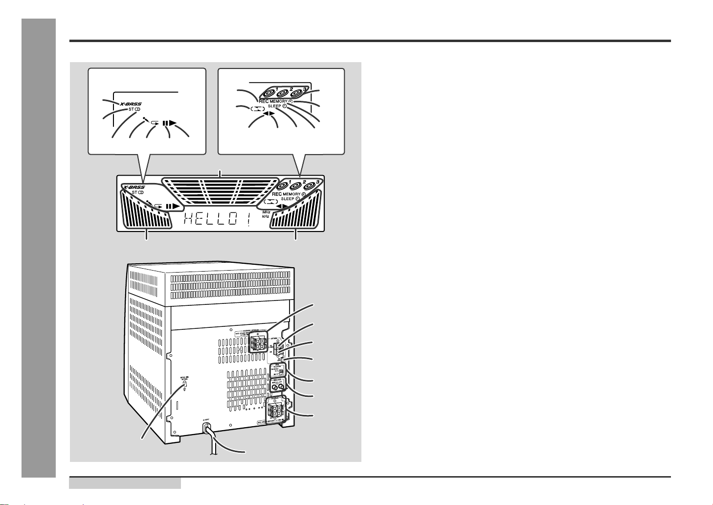
CD-BK250W/CD-BK2600W/CD-BK270W
– 40 –
T
T
DATA
DATACK
LRSY
Stopped
CH1=2 V
DC 10:1
CH2=2 V
DC 10:1
CH3=2 V
DC 10:1
5 µs/div
(5 µs/div)
NORM:100 kS/s
1
2
3
=Record Length=
Smoothing : ON CH1 : 0.00 V
CH2 : 0.00 V
Main : 5 K
Zoom : 100
Mode : AUTO
Type : EDGE CH3
Delay : 0.0 ns
Hold off : 0.2 µs
CH3 : 0.00 V
CH4 : 0.00 V
BW : FULL
=Trigger==Filter= =Offset=
CH3
v/DIV
2 V
1999/04/05 20:50:17
10
IC1 58
IC1 59
IC1 60
11
12
T
T
DOUT
Stopped
CH1=2 V
DC 10:1
500 ns/div
1999/04/07 09:25:28
(500 ns/div)
NORM:200 MS/s
1
=Record Length=
Smoothing : ON CH1 : 0.00 V
CH2 : 0.00 V
Main : 1 K
Zoom : 100
Mode : NORMAL
Type : EDGE CH1
Delay : 2.887 ms
Hold off : 0.2 µs
CH3 : 0.00 V
CH4 : 0.00 V
BW : FULL
=Trigger==Filter= =Offset=
9
IC1 39
T
FDO
PDO2
PDO1
Stopped
CH1=500 mV
DC 10:1
CH3=1 V
DC 10:1
CH4=1 V
DC 10:1
500 ms/div
(500 ms/div)
NORM:20 kS/s
1
4
3
=Record Length=
Smoothing : ON CH1 : 0.000 V
CH2 : 0.0 V
Main : 100 K
Zoom : 2 K
Mode : AUTO
Type : EDGE CH2
Delay : 0.0 ns
Hold off : 0.2 µs
CH3 : 0.00 V
CH4 : 0.00 V
BW : FULL
=Trigger==Filter= =Offset=
CH1
v/DIV
500 mV
1999/04/05 17:33:17
1
IC1 21
7
IC1 73
8
IC1 74
T
T
FDO
SPDO
Stopped
CH1=200 mV
DC 10:1
CH2=500 mV
DC 10:1
500 ms/div
1999/04/07 09:51:15
(500 ms/div)
NORM:20 kS/s
2
1
=Record Length=
Smoothing : ON CH1 : 0.000 V
CH2 : 0.000 V
Main : 100 K
Zoom : 2 K
Mode : NORMAL
Type : EDGE CH2
Delay : 2.924 ms
Hold off : 0.2 µs
CH3 : 0.00 V
CH4 : 0.00 V
BW : FULL
=Trigger=
=Filter= =Offset=
1
IC1 21
6
IC1 22
T
T
TE
DRF
Stopped
CH1=10 V
DC 10:1
CH2=1 V
DC 10:1
100 ms/div
(100 ms/div)
NORM:100 kS/s
2
1
=Record Length=
Smoothing : ON CH1 : 0.0 V
CH2 : 0.00 V
Main : 100 K
Zoom : 2 K
Mode : NORMAL
Type : EDGE CH1
Delay : 2.924 ms
Hold off : 0.2 µs
CH3 : 0.00 V
CH4 : 0.00 V
BW : FULL
=Trigger=
=Filter= =Offset=
3
IC1 67
4
IC1 15
Vp-p=1.0 V~1.3 V
0.5 mV/div,0.5 µsec/div
5
IC1 4
T
FDO
DRF
TE
Stopped
CH1=500 mV
DC 10:1
CH2=10 V
DC 10:1
CH3=1 V
DC 10:1
500 ms/div
(500 ms/div)
NORM:20 kS/s
1
2
3
=Record Length=
Smoothing : ON CH1 : 0.000 V
CH2 : 0.0 V
Main : 100 K
Zoom : 2 K
Mode : AUTO
Type : EDGE CH1
Delay : 0.0 ns
Hold off : 0.2 µs
CH3 : 0.00 V
CH4 : 0.00 V
BW : FULL
=Trigger==Filter= =Offset=
-3 div -1 div 0 div +1 div +3 div
CH Position To
CH2
Position
0.20 div
1
IC1 21
3
IC1 67
4
IC1 15
T
FDO
TDO
Stopped
CH1=500 mV
DC 10:1
CH3=500 mV
DC 10:1
500 ms/div
(500 ms/div)
NORM:20 kS/s
1
3
=Record Length=
Smoothing : ON CH1 : 0.000 V
CH2 : 0.0 V
Main : 100 K
Zoom : 2 K
Mode : AUTO
Type : EDGE CH1
Delay : 0.0 ns
Hold off : 0.2 µs
CH3 : 0.000 V
CH4 : 0.00 V
BW : FULL
=Trigger==Filter= =Offset=
CH1
v/DIV
500 mV
1
IC1 21
2
IC1 20
WAVEFORMS OF CD CIRCUIT
– 41 –
CD-BK250W/CD-BK2600W/CD-BK270W
Parts code
1. CD optical pickup Lens cleaner disc UDSKA0004AFZZ
HOW TO USE
CAUTION
Cleaning fluid
Cleaner disc
Using the brush in the cleaner cap, apply 1 or 2 drops of the cleaning fluid to the
brush on the CD cleaner disc which has the mark next to it.
Place the CD cleaner disc onto the CD disc tray with the brush side down,then
press the play button.
You will hear music for about 20 seconds and the CD player will automatically stop.
If it continuous to turn, press the stop button.
1.
2.
3.
The CD lens cleaner should be effective for 30-50 operations, however if the
brushes become worn out earlier then please the cleaner disc.
If the CD cleaner brushes become very wet then wipe off any excess fluid with a soft
cloth.
Do not drink the cleaner fluid or allow it to come in contact with the eyes. In the
event of this happening then drink and / or rinse with clean water and seek medical
advice.
The CD cleaner disc must not be used on car CD players or on computer CD-ROM
drives.
All rights reserved. Unauthorized duplicating, broadcasting and renting this product
is prohibited by law.
TROUBLE SHOOTING
When the CD does not function
When the CD section does not operate when the objective lens of the optical pickup is dirty, this section may not operate. Clean
the objective lens, and check the playback operation. When this section does not operate even after the above step is taken, check
the following items.
Remove the cabinet and follow the trouble shooting instructions.
"Track skipping and/or no TOC (Table Of Contents) may be caused by build up of dust other foreign matter on the laser pickup
lens. Before attempting any adjustment make certain that the lens is clean. If not, clean it as mentioned below."
Turn off the power, and wipe the lens softly using a cleaning paper moistened with commercially available cleaning solution so
as not to damage it. Be careful not to touch the lens with bare hands.
Dust gradually accumulates on the objective lens during use, and it may degrade performance. To avoid this problem, use a
cleaning disc designed for CD optical pickup lenses.
When a CD cannot be played
1. "E-CD01" is displayed.
(1) Check the power to IC1 (LC78645E), the presence of the clock signal (33.8688 MHz) and the status of the RESET terminal
(pin 66 on IC1).
(2) Does the pickup move to the PICKUP-IN Switch (SW4) position?
If (1) and (2) are OK, check the system microcomputer (especially the communication line with the DSP).
2. Pressing the CD operation key is accepted, but playback does not occur.
(1) Focus-HF system check
(2) Tracking system check
(3) Spin system check
(4) PLL system check
(5) Others
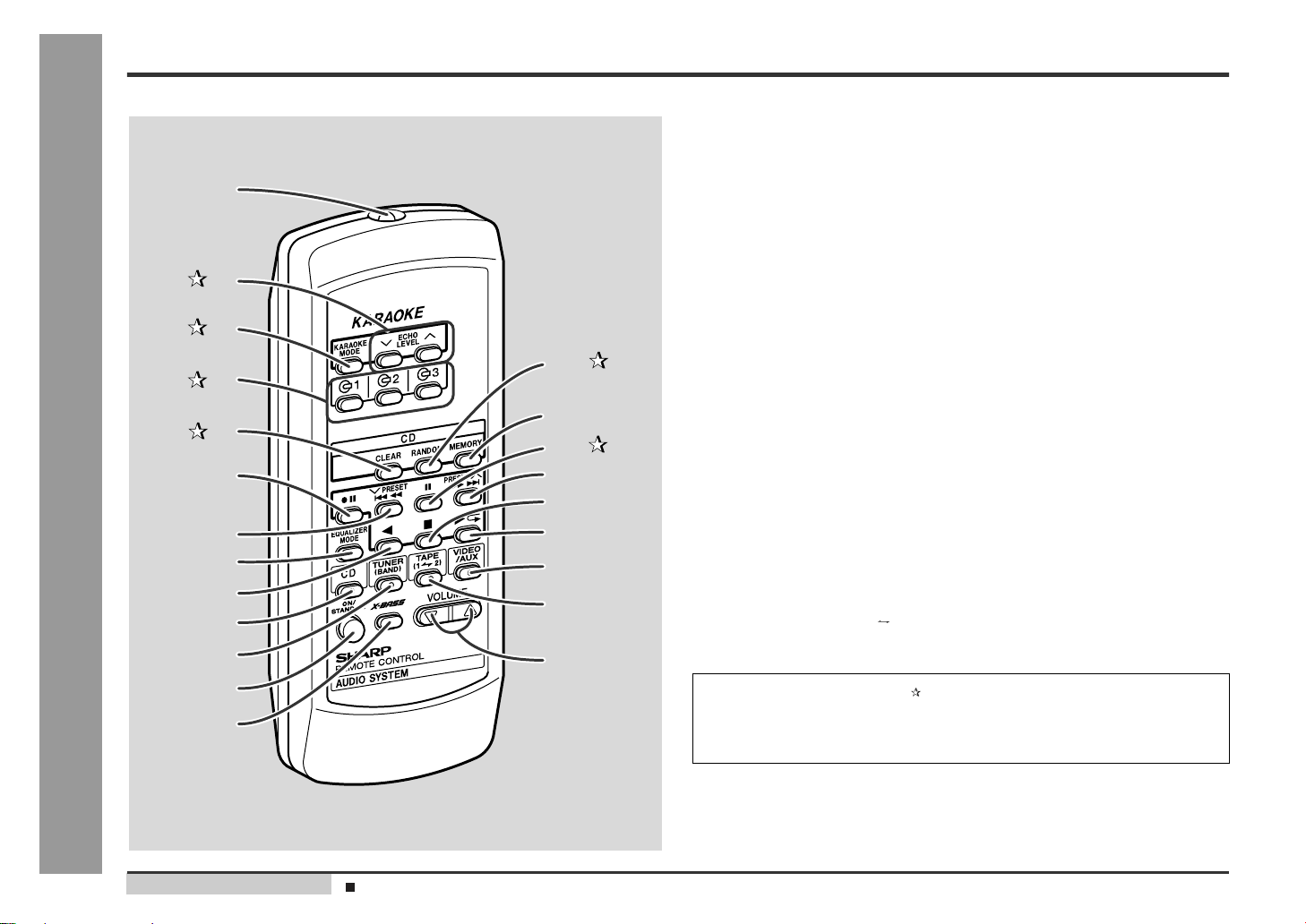
CD-BK250W/CD-BK2600W/CD-BK270W
– 42 –
Vp-p=1.0 V~1.3 V
0.5 mV/div,0.5 µsec/div
T
FDO
DRF
TE
Stopped
CH1=500 mV
DC 10:1
CH2=10 V
DC 10:1
CH3=1 V
DC 10:1
500 ms/div
(500 ms/div)
NORM:20 kS/s
1
2
3
=Record Length=
Smoothing : ON CH1 : 0.000 V
CH2 : 0.0 V
Main : 100 K
Zoom : 2 K
Mode : AUTO
Type : EDGE CH1
Delay : 0.0 ns
Hold off : 0.2 µs
CH3 : 0.00 V
CH4 : 0.00 V
BW : FULL
=Trigger==Filter= =Offset=
-3 div -1 div 0 div +1 div +3 div
CH Position To
CH2
Position
0.20 div
T
FDO
TDO
Stopped
CH1=500 mV
DC 10:1
CH3=500 mV
DC 10:1
500 ms/div
(500 ms/div)
NORM:20 kS/s
1
3
=Record Length=
Smoothing : ON CH1 : 0.000 V
CH2 : 0.0 V
Main : 100 K
Zoom : 2 K
Mode : AUTO
Type : EDGE CH1
Delay : 0.0 ns
Hold off : 0.2 µs
CH3 : 0.000 V
CH4 : 0.00 V
BW : FULL
=Trigger==Filter= =Offset=
CH1
v/DIV
500 mV
If the level is not normal.
1. Is focus servo activated ?
(Waveform drawing Figure 42-2)
Pins 7~12, 79 and 80 on IC1
Check the laser diode driver Q1 peripheral circuit.
When a disc is loaded, start playback operation.
2. Does DRF change from "L" to "H" ?
Is the disc rotating ?
3. Is the HF waveform normal ?
(Waveform drawing Figure 42-3)
Check the spin system.
If the disc is spinning and a HF waveform is generated,
DRF will go H.
Figure 42-1
Check the laser diode driver Q1 peripheral circuit.
(1) Focus-HF system check.
Although a CD is inserted and the cover is closed, "NO
DISC" is displayed.
1. Does the pickup move to the PICKUP-IN Switch (SW4)
position ?
Sled motor (M2).
Press the OPEN/CLOSE switch (SW1) without inserting a
disc, and try starting the playback operation.
2. Does the focus (lens) move up and down ?
(Waveform drawing Figure 42-1).
Check the focus peripheral circuit.
3. Is the laser lit ?
Spindle motor (M1).
4. Is the turntable rotating ?
Figure 42-2
Figure 42-3
Yes
Yes
Yes
No
No
No
No
No
No
No
Yes
Yes
No
– 43 –
CD-BK250W/CD-BK2600W/CD-BK270W
T
T
FDO
SPDO
Stopped
CH1=200 mV
DC 10:1
CH2=500 mV
DC 10:1
500 ms/div
1999/04/07 09:51:15
(500 ms/div)
NORM:20 kS/s
2
1
=Record Length=
Smoothing : ON CH1 : 0.000 V
CH2 : 0.000 V
Main : 100 K
Zoom : 2 K
Mode : NORMAL
Type : EDGE CH2
Delay : 2.924 ms
Hold off : 0.2 µs
CH3 : 0.00 V
CH4 : 0.00 V
BW : FULL
=Trigger=
=Filter= =Offset=
T
T
TE
DRF
Stopped
CH1=10 V
DC 10:1
CH2=1 V
DC 10:1
100 ms/div
(100 ms/div)
NORM:100 kS/s
2
1
=Record Length=
Smoothing : ON CH1 : 0.0 V
CH2 : 0.00 V
Main : 100 K
Zoom : 2 K
Mode : NORMAL
Type : EDGE CH1
Delay : 2.924 ms
Hold off : 0.2 µs
CH3 : 0.00 V
CH4 : 0.00 V
BW : FULL
=Trigger=
=Filter= =Offset=
The tracking servo is not activated.
Check the peripheral circuits at pins 14, 15 and 20 on IC1, and
CNS1A/B.
If the waveform shown in Figure 43-1 appears and soon after
NO DISC appears ?
(2) Tracking system check.
Check the TE waveform at pin 15 on IC1.
A normal jump operation cannot be completed or the beginning of
the track cannot be found.
Check the around pin 20 on IC1.
"Initialization" is possible, but play is not possible ?
Data cannot be read. Check the VCO-PLL system.
"Initialization" is not possible.
Figure 43-1
Figure 43-2
Press the OPEN/CLOSE switch without inserting a disc, and
then try starting the play operation.
(3) Spin system check.
The spin driver circuit is OK.
1. The turntable rotates a little ?
(Waveform drawing Figure 43-2)
Check around pin 22 on IC1, pins 15 and 16 on IC3, and CNS3A/B.
2. The turntable doesn't rotate.
No
Yes
No
Yes
Yes
No
CD-BK250W/CD-BK2600W/CD-BK270W
– 44 –
T
T
DOUT
Stopped
CH1=2 V
DC 10:1
500 ns/div
1999/04/07 09:25:28
(500 ns/div)
NORM:200 MS/s
1
=Record Length=
Smoothing : ON CH1 : 0.00 V
CH2 : 0.00 V
Main : 1 K
Zoom : 100
Mode : NORMAL
Type : EDGE CH1
Delay : 2.887 ms
Hold off : 0.2 µs
CH3 : 0.00 V
CH4 : 0.00 V
BW : FULL
=Trigger=
=Filter= =Offset=
T
FDO
PDO2
PDO1
Stopped
CH1=500 mV
DC 10:1
CH3=1 V
DC 10:1
CH4=1 V
DC 10:1
500 ms/div
(500 ms/div)
NORM:20 kS/s
1
4
3
=Record Length=
Smoothing : ON CH1 : 0.000 V
CH2 : 0.0 V
Main : 100 K
Zoom : 2 K
Mode : AUTO
Type : EDGE CH2
Delay : 0.0 ns
Hold off : 0.2 µs
CH3 : 0.00 V
CH4 : 0.00 V
BW : FULL
=Trigger==Filter= =Offset=
CH1
v/DIV
500 mV
1999/04/05 17:33:17
Is pin 52 (C2F) on IC1 "L" ?
Yes
No
The HF waveform is normal and the time is displayed
normally, but no sound is produced. Or the sound
has dropouts.
(5) Others.
There are too many error flags on a damaged disc which
makes error correction impossible.
Check again using a known good disc.
1. When playing at normal speed.
Check the peripheral circuit at pin 39 (DOUT) on IC1 and
the waveform (Figure 44-2).
If OK, Check the unit.
When a disc is loaded, start play operation.
(4) PLL system check.
The HF waveform is normal, but the TOC data cannot be
read.
Check the PDO waveform. (Figure 44-1)
Check around pins 73~78 on IC1.
Figure 44-1
Figure 44-2

– 45 –
CD-BK250W/CD-BK2600W/CD-BK270W
FUNCTION TABLE OF IC
IC1 VHiLC78645E-1: CD Servo (LC78645E) (1/2)
1 SLCO Output — Control output.
2 SLCIST Input —
Resistor connection terminal for SLCO output current
setting.
3 EFMIN Input — RF signal input terminal.
4 RF Output — RF signal monitor terminal.
5 RFVDD Input — RF power terminal.
6 RFVSS — — RF earth terminal. To be connected to 0 V.
7 FIN1 A Input — A+C signal input terminal.
8 FIN2 B Input — B+D signal input terminal.
9 TIN1 E Input — E signal input terminal.
10 TIN2 F Input — F signal input terminal.
11 VREF Output RFVDD/2 VREF voltage output terminal.
12 REFI Input — Reference supply setting terminal.
13* FE Output ZHI FE signal monitor terminal.
14 TEC Output — LPF capacitor connection terminal for TE signal.
15* TE Output ZHI TE signal monitor terminal.
16* RFMON Output ZHI RF internal signal monitor terminal.
17 JITTC — — Capacitor connection terminal for jitter detection.
18 ADAVDD Input — Power terminal for servo A/D, D/A.
19 ADAVSS — — Earth terminal for serve A/D, D/A. To be connected to 0 V.
20 TDO Output ADAVDD/2 Output terminal for tracking control. D/A output.
21 FDO Output ADAVDD/2 Output terminal for focus control. D/A output.
22 SPDO Output ADAVDD/2 Output terminal for spindle control. D/A output.
23 SLDO Output ADAVDD/2 Output terminal for sled control. D/A output.
24* GPDAC Output ADAVDD/2 Servo D/A general-purpose output terminal.
25 CONT4 Input/Output Input Mode General-purpose I/O terminal 4.
26 CONT5 Input/Output Input Mode General-purpose I/O terminal 5.
27* SBCK/CONT6 Input/Output Input Mode General-purpose I/O terminal 6 or
Subcode reading clock input terminal.
28 SBCK/FG Input — Subcode reading clock input terminal/FG signal input terminal/external
emphasis setting terminal. Terminal functions are set by commands. When
not used, connect to 0 V.
29* DEFECT Output L Defect terminal.
30* V/*P Output H Auto switching monitor output terminal for rough servo phase control. “H”:
rough servo, “L”: phase servo.
31* FSEQ Output L Sync signal detection output terminal.
The status changes to “H” when the sync signal detected in EFM and the
sync signal of internal generation are identified.
32* MONI1 Output L Internal signal monitor terminal 1.
33* MONI2 Output L Internal signal monitor terminal 2.
34* MONI3 Output L Internal signal monitor terminal 3.
35* MONI4 Output L Internal signal monitor terminal 4.
36* MONI5 Output L Internal signal monitor terminal 5.
37 VSS — — Digital system earth terminal. To be connected to 0 V.
38 VDD Input — Digital system power terminal.
39* DOUT Output L Digital OUT output terminal. (EIAJ format)
40 TEST Input L Input terminal for test. To be connected to 0 V.
41 LVDD Input — Power supply for Left channel.
42 LCHO Output LVDD/2 Left channel output.
43 LVSS — — GND for Left channel. Must be connected to 0 V.
Pin No.
Function
Terminal Name
Input/Output
Setting in Reset
Controlled by commands from the
microcomputer. When not used, set
them as input terminals and connect
to 0 V, or set them as output
terminals and leave open.
In this unit, the terminal with asterisk mark (*) is (open) terminal which is not connected to the outside.
Left channel
D/A converter
For slice level
control.
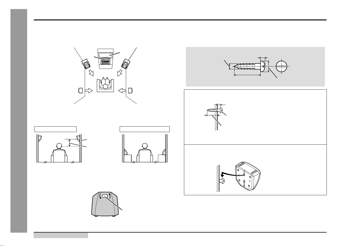
CD-BK250W/CD-BK2600W/CD-BK270W
– 46 –
44 RVSS — — GND for Right channel. Must be connected to 0 V.
45 RCHO Output LVDD /2 Right channel output.
46 RVDD Input — Power supply for Right channel.
47 XVDD Input — Power supply for crystal oscillator.
48 XOUT Output — Connected for the 33.8688 MHz crystal oscillator ciement.
49 XIN Input —
50 FSX/16MIN Input/Output Input 7.35 kHz Synchronization signal monitor port.
or Clock input port for Digital filter & D/A
51 XVSS — — Crystal GND for crystal oscillator. Must be connected to 0 V.
Oscillator
52* C2F Output H C2 FLAG monitor port.
53* EFLG Output L C1, C2 error corrected monitor port.
54* 16MOUT Output Clock 16.9344 MHz output port.
55 ASLRCK Input — Word clock input port.
(If this port does not use, must be connect to 0 V.)
56 ASDACK Input — Bit clock input port.
(If this port does not use, must be connect to 0 V.)
57 ASDFIN Input —
Left/Right channel data input port.
(If this port does not use, must be connect to 0 V.)
58* LRSY Output L Word clock output port.
59* DATACK Output L Digital data Bit clock output port.
60* DATA Output L Left/Right channel data output port.
61 CE Input — Chip enable signal input port.
62 CL Input —
Microcomputer
Data transfer clock input port.
63 DI Input — Interface Data input port.
64 DO Output (H) Data output port. (N-ch. open drain output.)
65 *WRQ Output H Interruption signal output.
66 *RES Input — Chip reset signal input port.
This port must be set LOW after first applied power on.
67 DRF Output L Focus detection output port.
68 VDD5 Input — Power supply for Microprocessor.
69 VSS — — GND for digital circuit. Must be connected to 0 V.
70 CONT3 Input/Output Input General purpose port 1.
71 CONT2 Input/Output Input General purpose port 2.
72* CONT1 Input/Output Input General purpose port 3.
73 PDO1 Output — Internal VCO control phase comparator output port 1.
74 PDO2 Output Input Internal VCO control phase comparator output port 2.
75 VVSS — — GND for internal VCO. Must be connected to 0 V.
76 PCKIST Input — PDO output current adjustment resistor connection port.
77 VVDD Input — Power supply for internal VCO.
78 FR Input — VCO frequency range adjustment port.
79 LDS Input — LASER power detected signal input port.
80 LDD Output — LASER power control signal output port.
IC1 VHiLC78645E-1: CD Servo (LC78645E) (2/2)
Pin No.
Function
Terminal Name
Input/Output
Setting in Reset
Right channel
D/A converter
Crystal
Oscillator
Anti-shock
Controlled with serial data command from micro-
computer. When not used, General purpose input/
output terminal 7. set it as the input terminal and open
it by connecting to 0 V, or set it as the output terminal
and open it.
PLL
In this unit, the terminal with asterisk mark (*) is (open) terminal which is not connected to the outside.
Be sure to supply the same potential to each power terminal. (VVDD, ADAVDD, VDD, LVDD, RVDD, XVDD)
Terminal witch is controlled by the power terminal (VDD5 V) for a microcomputer interface :
CE (61 pin), CL (62 pin), DI (63 pin), DO (64 pin), WRQ (65 pin), RES (66 pin), DRF (67 pin)
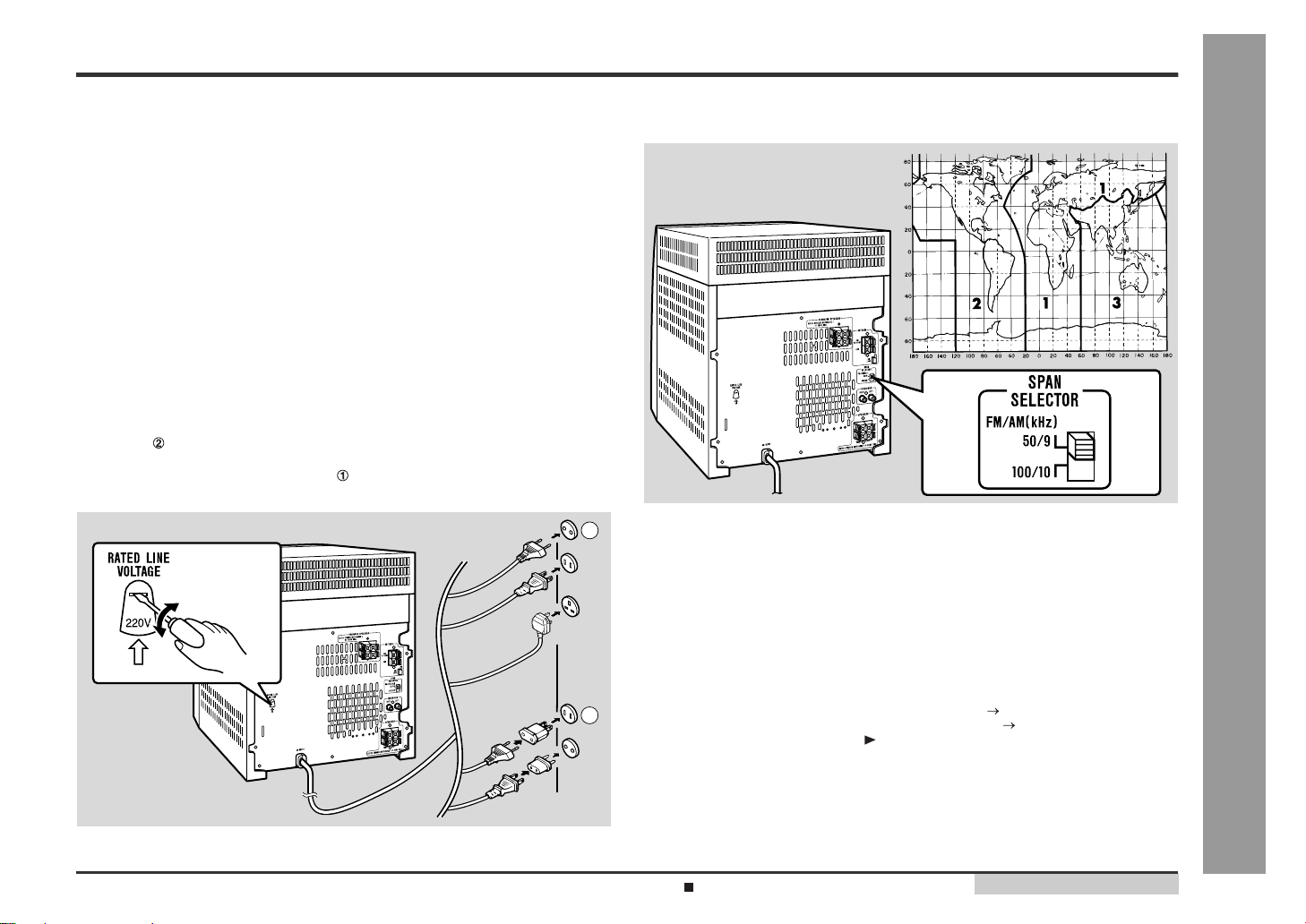
– 47 –
CD-BK250W/CD-BK2600W/CD-BK270W
Figure 47 BLOCK DIAGRAM OF IC
IC1 VHiLC78645E-1: CD Servo (LC78645E)
1
2
3
4
5
6
7
8
9
10
11
12
13
14
15
16
17
18
19
20
21 22 23 24 25 26 27 28 29 30 31 32 33 34 35 36 37 38 39 40
80 79 78 77 76 75 74 73 72 71 70 69 68 67 66 65 64 63 62 61
60
59
58
57
56
55
54
53
52
51
50
49
48
47
46
45
44
43
42
41
SLCO
SLCIST
EFMIN
RF
RFVDD
RFVSS
FIN1 A
FIN2 B
TIN1 E
TIN2 F
VREF
REFI
FE
TEC
TE
RFMON
JITTC
ADAVDD
ADAVSS
TDO
FDO
SPDO
SLDO
GPDAC
CONT4
CONT5
SBCK/CONT6
SBCK/FG
DEFECT
V/*P
FSEQ
MONI1
MONI2
MONI3
MONI4
MONI5
(3.3 V)VSS
VDD
DOUT
TEST
LDD
LDS
FR
VVDD
PCKIST
VVSS
PD02
PD01
CONT1
CONT2
CONT3
VSS
VDD5
DRF
*RES
*WRQ
DO
DI
CL
CE
DATA
DATACK
LRSY
ASDFIN
ASDACK
ASLRCK
16MOUT
EFLG
C2F
XVSS
FSX/16MIN
XIN
XOUT
XVDD
RVDD
RCHO
RVSS
LVSS
LCHO
LVDD
LC78645E
+
–
+
–
+
–
+
–
–
–
+
+
MIX
LPF
LPF
LPF
TBAL
TBAL
RAM
LEVEL SET
AGC EQ
SW
PH
BH
+
–
+
–
+
–
+
–
MONI
CONT
A/D
SERVO PROCESSOR
TRACK JUMP
AUTO ADJUST
JITTER
DETECT
1bit DAC
8FS
DIGITAL FILTER
GENERAL-PURPOSE
PORTS
COMMAND
INTERFACE
CLOCK
GENERATOR
CLV,CAV
CONTROL
PLL
VCEC
SLICE LEVEL
CONTROL
APC
S/H
D/A
SW
DRF
RUPTURE DEFECT
FRAME SYNC
DETECT,PROTECT INSERT,
EFN DECODE
VDD
SUBCODE DECODE CRC
MONITOR SIGNAL SELECTOR
RAM
ERROR
CORRECTION
AUDIO CD
AUDIO OUT
SERIAL
OUT
EXTERNAL
AUDIO IN
INTERPOLATION
MUTE
ATTENUATION
DEEMPHSIS
LPF
FIN1 A
FIN2 B
TIN1 E
TIN2 F
REF1
DETECT
ADIN
ADAVDD
ADAVSS
JITTC
SLCO
EFMIN
SLCIST
PCK
PDO1
PDO2
FR
PCKIST
VVDD
VVSS
SBCK/FG
XIN
XOUT
16MOUT
XVDD
XVSS
*RES
*WRQ
CL
CE
DI
DO
VDD5V
CONT1, 2, 3
TEST
CONT4, 5
SBCK/CONT6
LVDD
LVSS
LCHO
RCHO
RVDD
RVSS
ASDFIN
ASDQCK
ASLRCK
DATA
DATACK
LRSY
DOUT
EFLG
C2F
FSK/16MIN
MONI1~5
VSS
VDD
V/*P
FSEQ
DRF
GPDAC
SPDO
SLDO
TDO
FDO
LDS
LDD
VREF
RFMON
RFVSS
RFVDD
RF
TEC
TE
FE
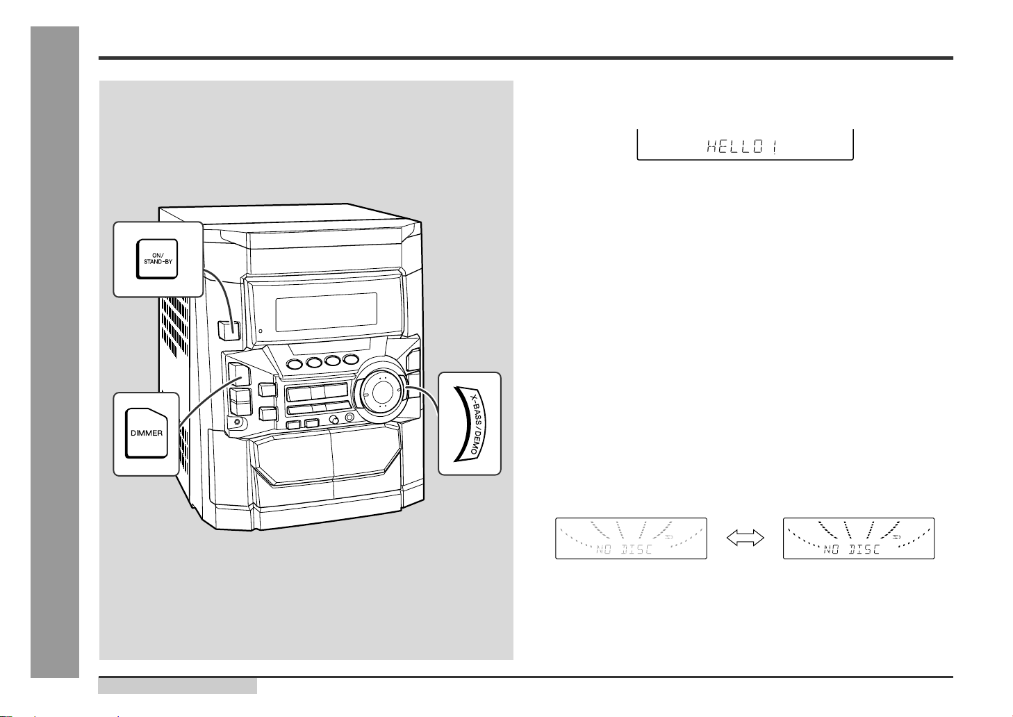
CD-BK250W/CD-BK2600W/CD-BK270W
– 48 –
1 VDD VDD Input (+) POWER SUPPLY.
2 P37 -20 dB ATT Output -20 dB ATTENUATOR.
3 P36 NO USE Output GND
DSA_STB Input/Output DSA STRUBE
4 P35 T_BIAS Output TAPE RECORD BIAS.
5 P34 T_T1/T2 Output TAPE T1/T2 CHANGE.
6 P33 REC/PLAY Output TAPE REC/PLAY CHANGE.
7 P32 RES OUT Output CD DSP RESET & MPEG MICROCOMPUTER RESET.
8 P31 DRF Input CD RF LEVEL DETECTION.
9 P30 WRQ Input CD DSP WRITE REQUEST.
10 RESET RESET Input RESET.
11 X2 X2 Output MAIN CLOCK.
12 X1 X1 Input MAIN CLOCK.
13 VPP/IC XVPP/IC — GND
14* XT2 XT2 — OPEN.
15 P04 SPN Input TUNER SPAN CHANGE.
16 VDD VDD Input (+) POWER SUPPLY.
17 P27 CD CLK Output CD DSP CLOCK.
18 P26 CD DI Output CD DSP COMMAND.
19 P25 CD DO Input CD DSP CODE Q OUT.
20 P24 CD CE Output CD DSP CE OUTPUT.
21 P23 CE Output CE OUTPUT.
22 P22 CLK Output CLOCK OUTPUT.
23 P21 DI Output DATA OUTPUT.
24 P20 DO Input DATA INPUT.
25 AVSS AVSS — ANALOG GROUND.
26 ANI7 O/C SW Input CD OPEN/CLOSE SWITCH.
DISC NO SW Input CD DISC NUMBER SWITCH.
DSA_DATA Input/Output DS DATA INPUT.
27 ANI6 NO USE Input GND
TUNER SM Input TUNER SIGNAL METER INPUT.
DSA_ACK Input/Output DSA ACR.
28 ANI5 SPEANA 2 Input SPEANA DATA INPUT 16 kHz.
29 ANI4 SPEANA 1 Input SPEANA DATA INPUT 1 kHz.
30 ANI3 SPEANA 0 Input SPEANA DATA INPUT 63 kHz.
31-33 ANI2-ANI0 KEY 2-KEY 0 Input KEY INPUT.
34 AVDD AVDD Input ANALOG VDD.
35 AVREF AVREF Input ANALOG REF VOLTAGE.
36 INTP3 P_IN Input POWER FAILURE DETECT.
37 P02 JOG 1 Input JOG VOLUME INPUT 1.
38 P01 JOG 0 Input JOG VOLUME INPUT 0.
39 INTP0 REMOCON Input REMOCON INPUT.
40 VSS VSS — GROUND VOLTAGE.
41 P74 SMUTE Output SYSTEM MUTE CONTROL.
42 P73 T_SOL_B Output TAPE 2 SOLENOID CONTROL.
43 P72 T_SOL_A Output TAPE 1 SOLENOID CONTROL.
44 P71 T_MOTOR Output TAPE MOTOR CONTROL.
45 P70 TIMER LED Output TIMER LED CONTROL.
46 VDD VDD Input (+) POWER SUPPLY.
47* P127 AC RLY_CONT Output AC RELAY CONTROL.
48 P126 SP-RLY Output SPEAKER OUTPUT RELAY CONTROL.
49 P125 SP_DET Input SPEAKER OUTPUT DETECTION.
IC701 RH-iX0427AWZZ: System Microcomputer (IX0427AW) (1/2)
Port Name
Terminal Name
Pin No.
Input/Output
Function
In this unit, the terminal with asterisk mark (*) is (open) terminal which is not connected to the outside.
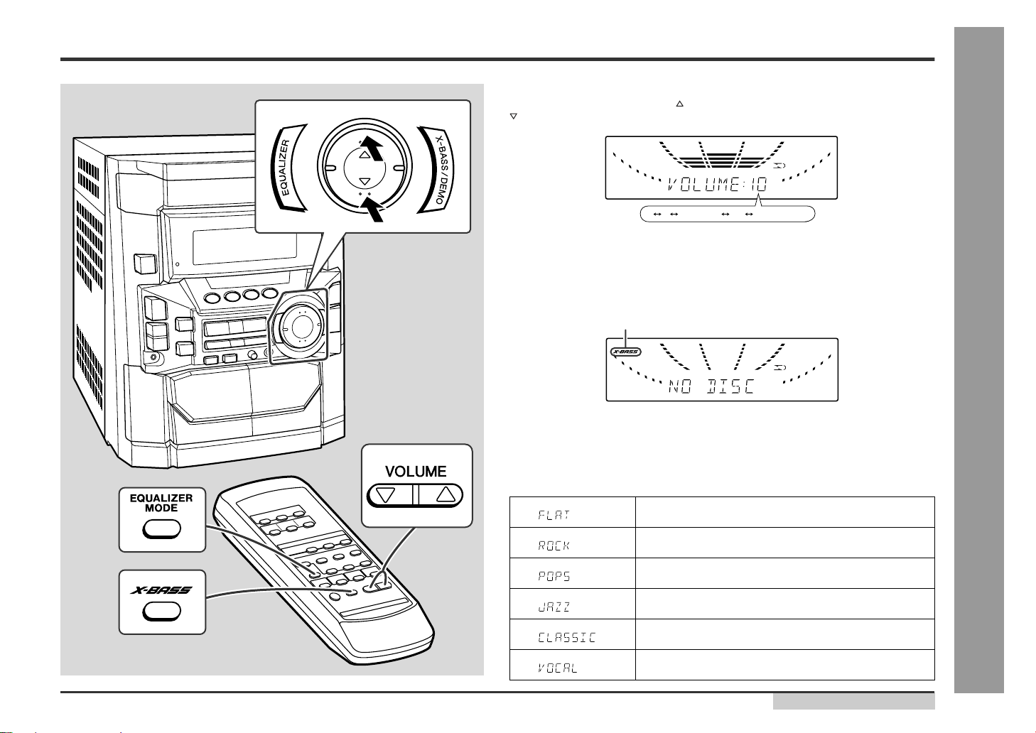
– 49 –
CD-BK250W/CD-BK2600W/CD-BK270W
50 P124 T 1 RUN Input TAPE 1 RUN PULSE INPUT.
51 P123 T 2 RUN Input TAPE 2 RUN PULSE INPUT.
52 P122 CD CLAMP SW Input CD CHANGER CLAMP SWITCH.
53 P121 NO USE Input GND
54 P120 PLAY SW_B Input PLAY SWITCH FOR T 2.
55 P117 FPA Input TAPE 2 A-SIDE FULL PROOF.
56 P116 FPB Input TAPE 2 B-SIDE FULL PROOF.
57 P115 MIC SW Input MIC SWITCH.
58* P114 LCK 0 Output LED DRIVER LCK.
59 P113
DISTOUT
Output DESTINATION OUTPUT.
60 FIP39 NO USE Output GND
61 FIP38 KARAOKE LATCH Output KARAOKE LATCH.
62 FIP37 NO USE Output GND
MPEG_POW Output MPEG POWER CONTROL.
63 FIP36 NO USE Output GND
RDS RST/ESS_ACK Output RDS FAN RESET.
64 FIP35 NO USE Input GND
RDS RDDA/ESS_STB Input RDS TRANSMIT DATA INPUT/DSA STROBE.
65 FIP34 NO USE Output GND
RDS RDCL/ESS_DI Output RDS CLOCK/DSA DATA OUTPUT.
66 FIP33 NO USE Input GND
RDS READY/ESS_DO Input RDS READY/DSA DATA INPUT.
67 P103 DIST3 Input DESTINATION INPUT.
FIP32 P22 Output FL DISPLAY DRIVER.
68 P102 DIST2 Input DESTINATION INPUT.
FIP31 P21 Output FL DISPLAY DRIVER.
69 P101 DIST1 Input DESTINATION INPUT.
FIP30 P20 Output FL DISPLAY DRIVER.
70 P100 DIST0 Input DESTINATION INPUT.
FIP29 P19 Output FL DISPLAY DRIVER.
71-78 FIP28-FIP21 P18-P11 Output FL DISPLAY DRIVER.
79 VLOAD VLOAD Input FL DRIVER (-) POWER SUPP. -30 V
80-89 FIP20-FIP11 P10-P1 Output FL DISPLAY DRIVER.
90-100 FIP10-FIP0 G11-G1 Output FL DISPLAY DRIVER.
IC701 RH-iX0427AWZZ: System Microcomputer (IX0427AW) (2/2)
Port Name
Terminal Name
Pin No.
Input/Output
Function
In this unit, the terminal with asterisk mark (*) is (open) terminal which is not connected to the outside.
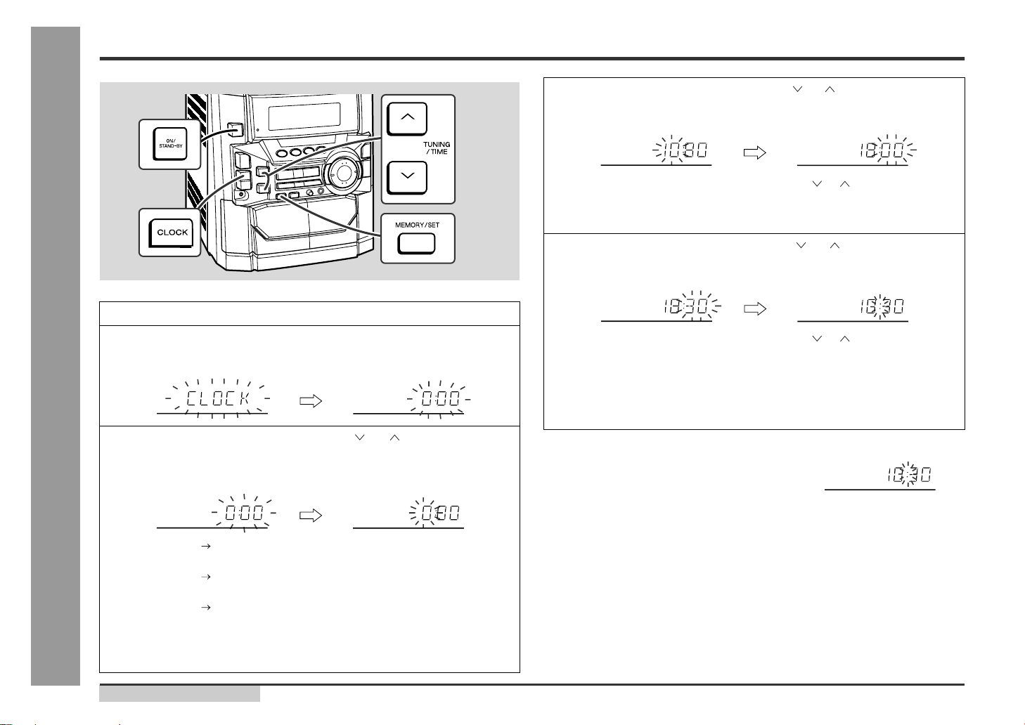
CD-BK250W/CD-BK2600W/CD-BK270W
– 50 –
IC601 VHiLC75341/-1: Audio Processor (LC75341)
Figure 50 BLOCK DIAGRAM OF IC
19
20
21
222324
123
4
5
6
7
8
9
10 11 12 13 14 15 16
18
17
LVref
RVref
CONTROL
CIRCUIT
CONTROL
CIRCUIT
CONTROL
CIRCUIT
LOUT
LBASS
LIN
LSEL0
L4
L3
L2 L1
R1 R2
R3 R4
RSEL0
R1N
RTRELTRE
RBASS
ROUT
VREF
VDD
CLK
DI
CE
VSS
CCB
INTERFACE
CD
Tuner
Tape
Video
24 23 22 21 20 19 18 17 16 15 14 13
123456789101112
LC75341
DI
CE
VSS
LOUT
LBASS
LTRE
LIN
LSEL0
L4
L3
L2
L1
CLK
VDD
VREF
ROUT
RBASS
RTRB
RIN
RSEL0
R4
R3
R2
R1
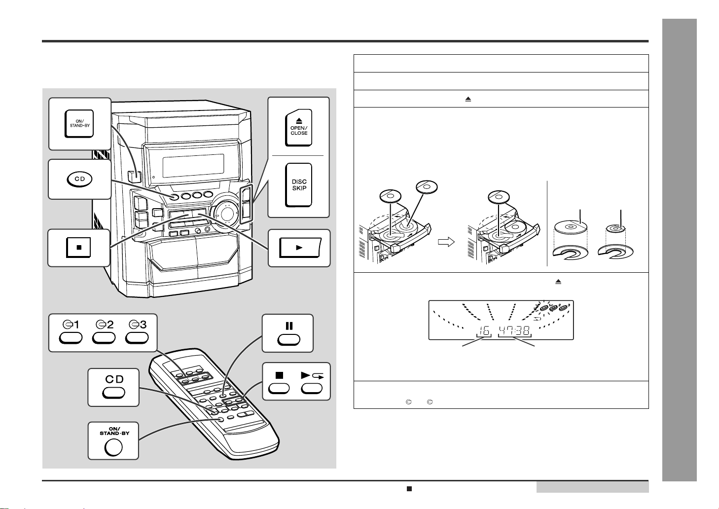
– 51 –
CD-BK250W/CD-BK2600W/CD-BK270W
1 MIC SW Input Microphone SW L: MIC OFF, H: MIC ON
2 MCLKCONT — Clock Control.
Controls built-in clock generation circuit with external R.
3 VALC — ALC operating voltage setting terminal.
To set ALC operating voltage according to applied voltage.
4 MIC1 IN Input Microphone 1 input.
To connect MIC 1.
5* ALC1 — ALC1 control.
To connect ALC1 attack/recovery time setting capacitor.
6* MIC1NFIN Input Microphone 1 negative feedback input.
To connect low cut-off frequency of MIC1 amplifier setting capacitor.
7* MIC1 OUT Output Microphone 1 output.
8 MIC1 VOLIN Input Microphone 1 volume input.
To connect capacitor to reduce noise generated at time of volume change.
9 MIC2 IN Input Microphone 2 input.
To connect MIC 2.
10 ALC2 — ALC2 control.
To connect ALC2 attack/recovery time setting capacitor.
11 MIC2 NFIN Input Microphone 2 negative feedback input.
To connect low cut-off frequency of MIC2 amplifier setting capacitor.
12 MIC2 OUT Output Microphone 2 output.
13 MIC2 VOLIN Input Microphone 2 volume input.
To connect capacitor to reduce noise generated at time of volume change.
14 MICOUT Output Microphone output.
Mixing output of MIC 1 and MIC 2.
15 LPF1IN1 Input Low pass filter 1 input 1.
Pre-filter before A/D convertor for digital delay.
16 LPF1 IN2 Input Low pass filter 1 input 2.
Pre-filter before A/D convertor for digital delay.
17 LPF1 OUT Output Low pass filter 1 output.
Pre-filter before A/D convertor for digital delay.
18 AD INTOUT Output A/D integrator output.
Composes D/A conversion integrator with external capacitor.
19 AD INTIN Input A/D integrator input.
Composes D/A conversion integrator with external capacitor.
20 ADCONT — A/D control.
To determine adaptive time constant of A/D convertor with ADM system.
21 REF — Reference power output.
To connect 1/2 Vcc output and filter capacitor.
22 GND — Ground.
23 VCC Input Power supply.
24 DACONT — D/A control.
To determine adaptive time constant of D/A convertor with ADM system .
25 DAINTIN Input D/A Integrator input.
Composes D/A conversion integrator with external capacitor.
26 DAINTOUT Output D/A Integrator output.
Composes D/A conversion integrator with external capacitor.
27 LPF2IN1 Input Low pass filter 2 input 1.
Post-filter after D/A convertor for digital delay.
28 LPF2IN2 Input Low pass filter 2 input 2.
Post-filter after D/A convertor for digital delay.
29 LPF2OUT Output Low pass filter 2 output.
Post-filter after D/A convertor for digital delay.
30 VOLIN Input Echo effect/Echo feed back volume input.
To connect capacitor to reduce noise generated at time of volume change.
31 L IN Input Lch line input.
32 R IN Input Rch line input.
ICK1 VHiM65856SP-1: Mic Amp. (M65856SP) (1/2)
Port NamePin No. Input/Output
Function
In this unit, the terminal with asterisk mark (*) is (open) terminal which is not connected to the outside.
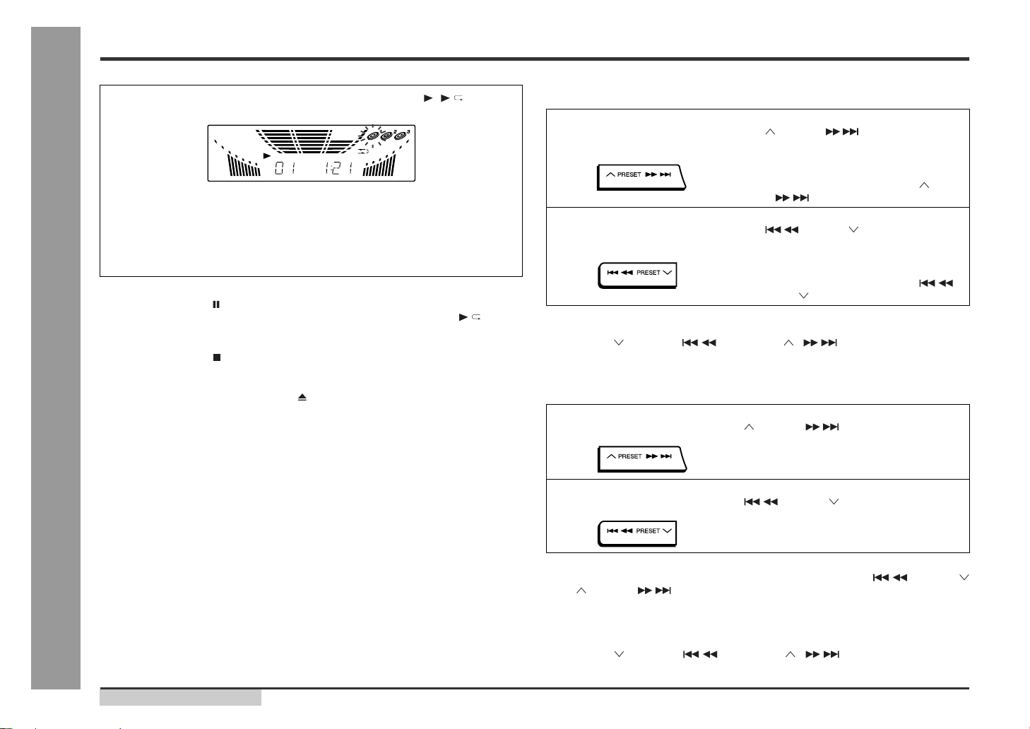
CD-BK250W/CD-BK2600W/CD-BK270W
– 52 –
ICK1 VHiM65856SP-1: Mic Amp. (M65856SP) (2/2)
In this unit, the terminal with asterisk mark (*) is (open) terminal which is not connected to the outside.
Function
33* KEYCONIN Input Monaural input for external KEYCONTROL IC.
Input/Output interface terminal for external KEYCONTROL IC.
34* SOURCEOUT Output Monaural input for external KEYCONTROL IC.
Input/Output interface terminal for external KEYCONTROL IC.
35 R OUT Output Rch mixing output.
36 L OUT Output Lch mixing output.
37 VCF IL — Vocal cut filter.
Processes frequencies lower then the vocal band.
38* PS1 Input Phase shift input 1.
Determines a constant at time of phase shift.
39* PS2 Input Phase shift input 2.
Determines a constant at time of phase shift.
40 LATCH Input Latch input via serial bus.
41 CLOCK Input Clock input via serial bus.
42 DATA Input Data input via serial bus.
42
DATA
41
CLOCK
40
LATCH
39
PS2
38
PS1
37
VCFIL
36
LOUT
35
ROUT
34
SOURCEOUT
33
KEYCONIN
32
RIN
31
LIN
30
VOLIN
29
LPF2OUT
28
LPF2IN2
27
LPF2IN1
26
DAINTOUT
25
DAINTIN
24
DACONT
23
VCC
22
1 2 3 4 5 6 7 8 9 10 11 12 13 14 15 16 17 18 19 20 21
GND
MIC SW
MCLKCONT
VALC
MIC1IN
ALC1
MCLK
MIC
VOL
MIC SW
(L,R)/2
L R STEREO
MIC1NFIN
MIC1OUT
MIC1VOLIN
MIC2IN
ALC2
MIC2NFIN
MIC2OUT
MIC2VOLIN
MICOUT
LPF1IN1
LPF1IN2
LPF1OUT
ADINTOUT
ADINTIN
ADCONT
REF
µ-COM I/F
PHASE
SHIFTER
SURROUND
ALC
ALC
MIC
VOL
ECHO
VOL
ECHO
F.BVOL
LPF
16kbit
SRAM
MAIN LOGIC
LPF D/A
VCC GND
ND
1/ZVcc
Figure 52 BLOCK DIAGRAM OF IC
Port NamePin No.
Input/Output
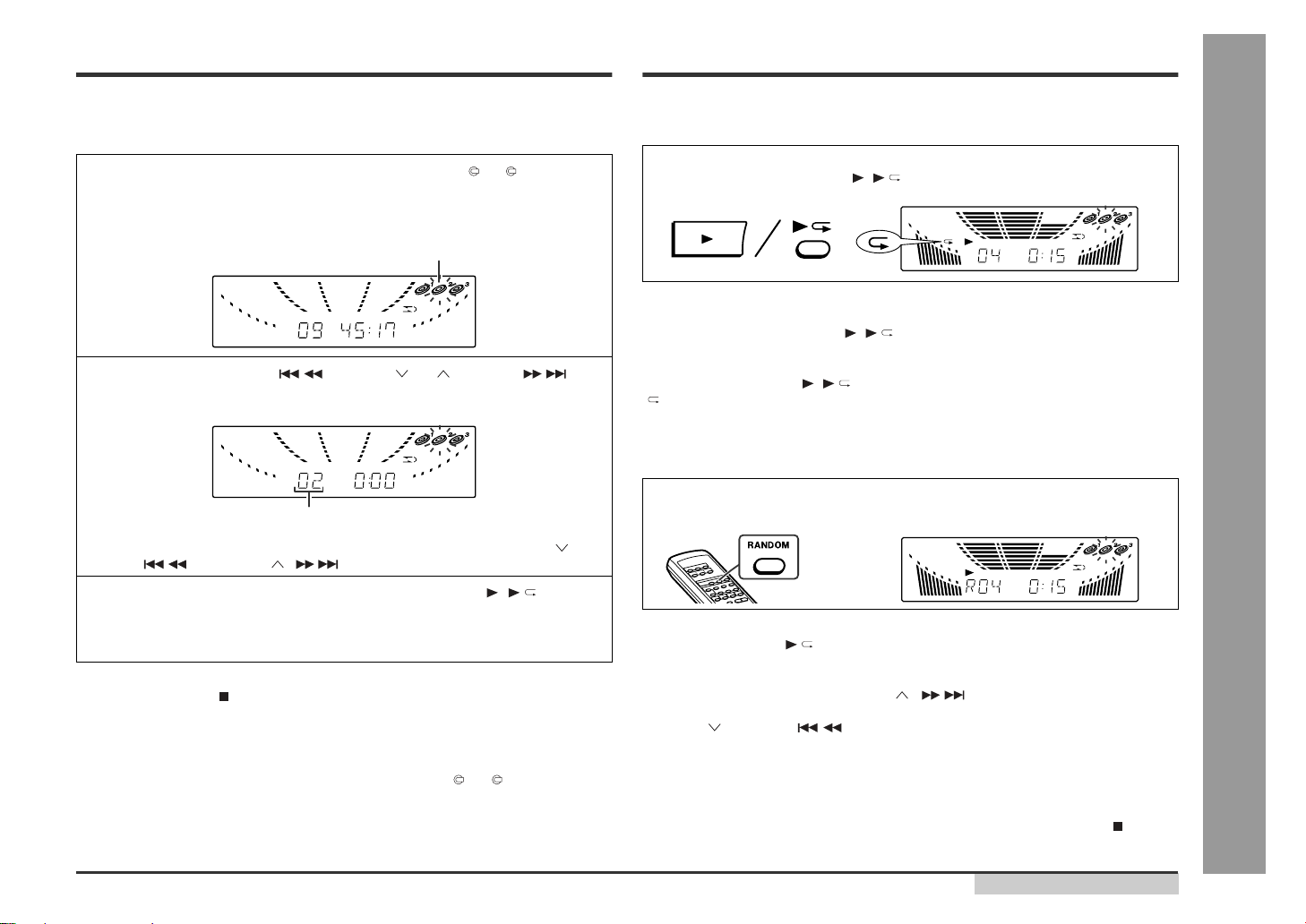
– 53 –
CD-BK250W/CD-BK2600W/CD-BK270W
FL701 VVKBJ749GNK-1: FL Display
FL DISPLAY
S1
9G
B1 B2 B3 B4 B5 B6 B7
B7 B6 B5 B4 B3 B2 B1
S5
1G 2G 3G 4G 5G 6G 7G 8G
11G 10G
S1
B8
B9
B10
B11
B12
B13
B14
S1S1
S1
S1
S4
S3
S2
col
f
a
bk
j
h
mg
c
n
e
r
p
Dp
d
B21
B20
B19
B18
B17
B16
B15
B1
B2
B3
B4
B5
B6
B7
11G
S1
B1
B2
B3
B4
B5
B6
B7
10G
S1
B1
B2
B3
B4
B5
B6
B7
B8
B9
B10
B11
B12
B13
B14
B15
B16
B17
B18
B19
B20
B21
9G
S1
B1
B2
B3
B4
B5
B6
B7
8G
Dp
d
c
n
p
r
e
m
g
b
k
j
h
f
a
S2
S3
S4
S5
7G
Dp
d
c
n
p
r
e
m
g
col
b
k
j
h
f
a
S2
S3
S4
S5
6G
Dp
d
c
n
p
r
e
m
g
b
k
j
h
f
a
S2
S3
S4
S5
5G
Dp
d
c
n
p
r
e
m
g
b
k
j
h
f
a
S2
S3
S4
S5
4G
Dp
d
c
n
p
r
e
m
g
b
k
j
h
f
a
S2
S3
S4
S5
3G
Dp
d
c
n
p
r
e
m
g
b
k
j
h
f
a
S2
S3
S4
S5
2G
Dp
d
c
n
p
r
e
m
g
b
k
j
h
f
a
S2
S3
S4
S5
1G
Dp
d
c
n
p
r
e
m
g
b
k
j
h
f
a
S2
S3
S4
S5
P1
P2
P3
P4
P5
P6
P7
P8
P9
P10
P11
P12
P13
P14
P15
P16
P17
P18
P19
P20
P21
P22
(Hiper)
(Lower)
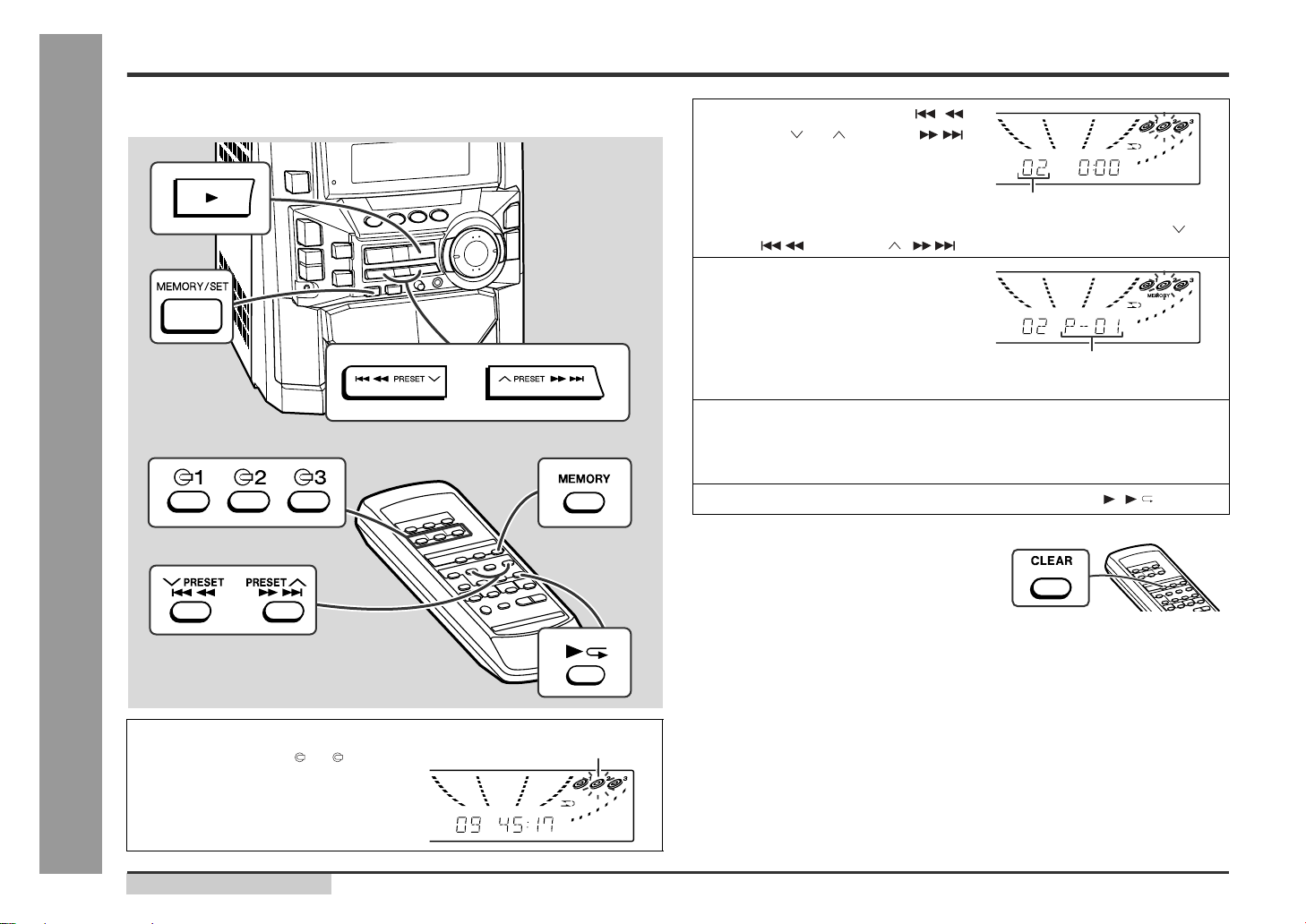
CD-BK250W/CD-BK2600W/CD-BK270W
– 54 –
–– MEMO ––
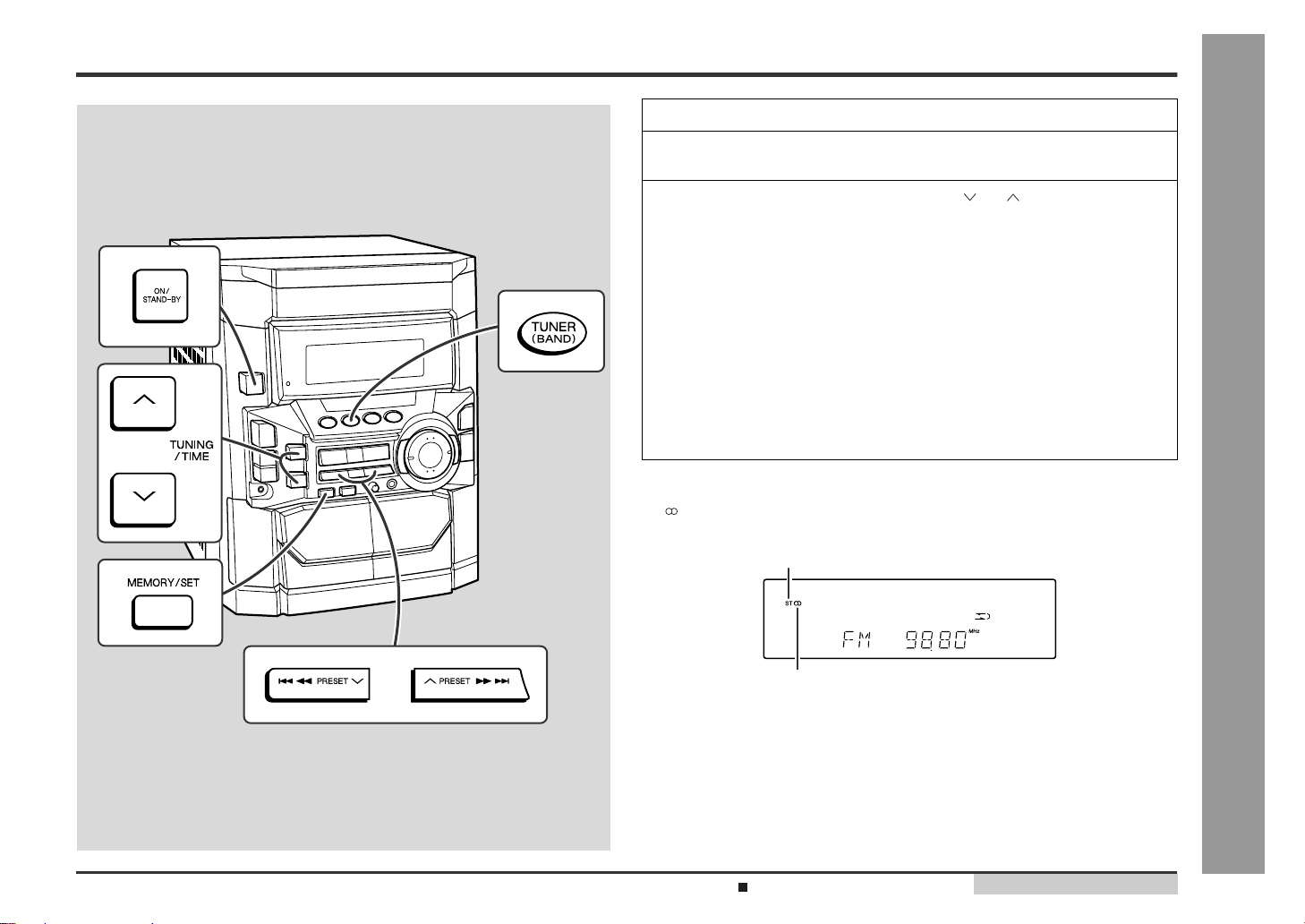
– 55 –
CD-BK250W/CD-BK2600W/CD-BK270W
PARTS GUIDE
NOTE:
Parts marked with “ ” are important for maintaining the safety of the set.
Be sure to replace parts with specified ones for maintaining the safety and performance of the set.
“HOW TO ORDER REPLACEMENT PARTS”
To have your order filled promptly and correctly, please furnish the
following information.
1. MODEL NUMBER 2. REF. No.
3. PART NO. 4. DESCRIPTION
MARK: SPARE PARTS-DELIVERY SECTION
For U.S.A. only
Contact your nearest SHARP Parts Distributor to order.
For location of SHARP Parts Distributor,
Please call Toll-Free;
1-800-BE-SHARP
Explanation of capacitors/resistors parts codes
Capacitors
VCC ....................... Ceramic type
VCK........................ Ceramic type
VCT ........................ Semiconductor type
VC • • MF ............... Cylindrical type (without lead wire)
VC • • MN............... Cylindrical type (without lead wire)
VC • • TV................ Square type (without lead wire)
VC • • TQ ............... Square type (without lead wire)
VC • • CY ............... Square type (without lead wire)
VC • • CZ ............... Square type (without lead wire)
VC • • • • • • • • • J .. The 13th character represents capacity difference.
("J" ±5%, "K" ±10%, "M" ±20%, "N" ±30%,
"C" ±0.25 pF, "D" ±0.5 pF, "Z" +80-20%.)
If there are no indications for the electrolytic capacitors, error is ±20%.
Resistors
VRD ....................... Carbon-film type
VRS........................ Carbon-film type
VRN ....................... Metal-film type
VR • • MF ............... Cylindrical type (without lead wire)
VR • • MN............... Cylindrical type (without lead wire)
VR • • TV................ Square type (without lead wire)
VR • • TQ ............... Square type (without lead wire)
VR • • CY ............... Square type (without lead wire)
VR • • CZ ............... Square type (without lead wire)
VR • • • • • • • • • J .. The 13th character represents error.
("J" ±5%, "F" ±1%, "D" ±0.5%.)
If there are no indications for other parts, the resistors are ±5%
carbon-film type.
MINI COMPONENT SYSTEM
MODEL CD-BK250W
CD-BK250W Mini Component System consisting of
CD-BK250W (main unit) and CP-BK250 (speaker system).
MINI COMPONENT SYSTEM
MODEL CD-BK2600W
CD-BK2600W Mini Component System consisting of
CD-BK2600W (main unit) and CP-BK2600 (speaker system).
MINI COMPONENT SYSTEM
MODEL CD-BK270W
CD-BK270W Mini Component System consisting of
CD-BK270W (main unit), CP-BK270 (front speakers) and
GBOXS0070AWM1 (surround speakers).
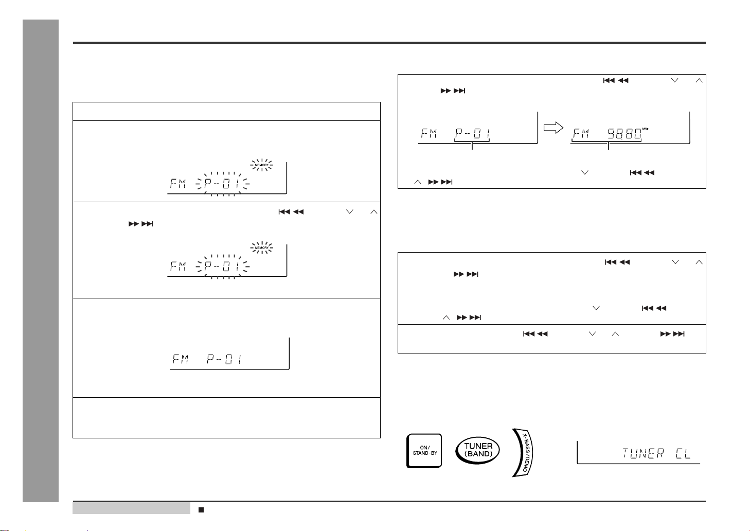
PRICE
RANK
DESCRIPTION
NO.
PARTS CODE
NO. PARTS CODE
PRICE
RANK
DESCRIPTION
CD-BK250W/CD-BK2600W/CD-BK270W
– 1 –
INTEGRATED CIRCUITS
IC1 VHILC78645E-1 J AY CD Servo,LC78645E
IC2 VHIM63001FP-1 J AX Focus/Tracking/Spin/Sled Driver,
M63001FP
IC101 VHIAN7345K/-1 J AM Playback and Record/Playback
Amp.,AN7345K
IC301 VHITA7358AP-1 J AG FM Front End,TA7358AP
IC302 VHILC72131/-1 J AP PLL (Tuner),LC72131
IC303 VHILA1832S/-1 J AN FM IF Det./FM Mpx./AM IF,
LA1832S
IC561,562 VHIKIA4558P-1 J AC Ope Amp.,KIA4558P
IC601 VHILC75341/-1 J AM Audio Processor,LC75341
IC701 RH-IX0427AWZZ J System Microcomputer,
IX0427AW
IC901 VHISTK4029S-1 J BA Power Amp.,STK4029S
IC902 VSKTC2026//-1 J AF Silicon,NPN,KTC2026
IC903 VHIKIA7810AP1 J AF Voltage Regulator,KIA7810AP
IC904 VHIKIA7805AP1 J AF Constant Voltage Regulator,
KIA7805AP
ICK1 VHIM65856SP-1 J AX Mic Amp.,M65856SP
ICK2 VHIKIA4558P-1 J AC Ope Amp.,KIA4558P
TRANSISTORS
Q1 VSKTA1266GR-1 J AB Silicon,PNP,KTA1266 GR
Q2 VSKTC3203Y/-1 J AC Silicon,NPN,KTC3203 Y
Q3 VSKRC102M//-1 J AC Digital,NPN,KRC102 M
Q101~104 VS2SC1845F/-1 J AC Silicon,NPN,2SC1845 F
Q105~108 VSKTC3199GR-1 J AB Silicon,NPN,KTC3199 GR
Q109 VSKTA1266GR-1 J AB Silicon,PNP,KTA1266 GR
Q110 VSKRC104M//-1 J AC Digital,NPN,KRC104 M
Q111 VSKTC3203Y/-1 J AC Silicon,NPN,KTC3203 Y
Q112 VSKTA1266GR-1 J AB Silicon,PNP,KTA1266 GR
Q113,114 VSKRC104M//-1 J AC Digital,NPN,KRC104 M
Q302 VSKTC3194Y/-1 J AD Silicon,NPN,KTC3194 Y
Q360 VSKTA1266GR-1 J AB Silicon,PNP,KTA1266 GR
Q601,602 VSKTC3199GR-1 J AB Silicon,NPN,KTC3199 GR
Q603,604 VSKTC3199GR-1 J AB Silicon,NPN,KTC3199 GR
Q701~703 VSKTC3199GR-1 J AB Silicon,NPN,KTC3199 GR
Q706 VSKTA1273Y/-1 J AE Silicon,PNP,KTA1273 Y
Q707,708 VSKTA1271Y/-1 J AC Silicon,PNP,KTA1271 Y
Q709 VSKRC102M//-1 J AC Digital,NPN,KRC102 M
Q901 VSKTA1274Y/-1 J AE Silicon,PNP,KTA1274 Y
Q902~905 VSKTC3199GR-1 J AB Silicon,NPN,KTC3199 GR
Q906 VSKTC3203Y/-1 J AC Silicon,NPN,KTC3203 Y
Q907 VSKRC107M//-1 J AC Digital,NPN,KRC107 M
Q908 VSKRA107M//-1 J AE Digital,PNP,KRA107 M
Q914 VSKTC3199GR-1 J AB Silicon,NPN,KTC3199 GR
QK1 VSKTC3203Y/-1 J AC Silicon,NPN,KTC3203 Y
DIODES
D1,2 VHDDS1SS133-1 J AB Silicon,DS1SS133
D301,302 VHDDS1SS133-1 J AB Silicon,DS1SS133
D305 VHDDS1SS133-1 J AB Silicon,DS1SS133
D561~563 VHDDS1SS133-1 J AB Silicon,DS1SS133
D690,691 VHDDS1SS133-1 J AB Silicon,DS1SS133
D701 VHDDS1SS133-1 J AB Silicon,DS1SS133
D705 VHDDS1SS133-1 J AB Silicon,DS1SS133
D709~716 VHDDS1SS133-1 J AB Silicon,DS1SS133
D901 VHDTS6B04GM-1 J AP Silicon,TS6B04GM
D902~908 VHDDS1N404S-1 J AB Silicon,DS1N404S
D911~916 VHDDS1SS133-1 J AB Silicon,DS1SS133
D917 VHDDS1N404S-1 J AB Silicon,DS1N404S
DK1,2 VHDDS1SS133-1 J AB Silicon,DS1SS133
LED701 VHPSLR342VCJ1 J AC LED,Red,SLR342VCJ1
ZD1 VHEDZ3R3BSB-1 J AB Zener,3.3V,DZ3.3BSB
ZD2 VHEDZ3R9BSB-1 J AC Zener,3.9V,DZ3.9BSB
ZD351 VHEDZ5R1BSB-1 J AC Zener,5.1V,DZ5.1BSB
ZD561 VHEDZ6R2BSB-1 J AC Zener,6.2V,DZ6.2BSB
ZD901 VHEDZ330BSD-1 J AC Zener,33V,DZ33BSB
ZD902 VHEDZ110BSB-1 J AB Zener,11V,DZ11BSB
ZD903 VHEDZ6R2BSA-1 J AB Zener,6.2V,DZ6.2BSA
ZD904 VHEDZ130BSB-1 J AB Zener,13V,DZ13BSB
ZD905 VHEDZ2R4BSB-1 J AB Zener,2.4V,DZ2.4BSB
ZDK1 VHEMTZJ5R6B-1 J AD Zener,5.6V,MTZJ5.6B
FILTERS
BF301 RFILR0008AWZZ J AE Band Pass Filter
CF303 RFILF0124AFZZ J AD FM IF,10.7 MHz
CF351 RFILF0003AWZZ J AK FM IF
CF352 RFILA0009AWZZ J AE AM IF
TRANSFORMERS
1 PT801 RTRNP0352AWZZ J Power
T301 RCILB0065AWZZ J AC FM OSC.
T302 RCILI0017AWZZ J AB FM IF
T303 RCILA0052AWZZ J AE AM Tracking
T306 RCILB0067AWZZ J AD AM OSC.
T351 RCILI0019AWZZ J AD AM IF
COILS
L1 VP-XHR82K0000 J AC 0.82 µH
L103 VP-MK331K0000 J AB 330 µH,Choke
L312 RCILR0056AWZZ J AB FM RF
L351 VP-DH101K0000 J AB 100 µH,Choke
L701 VP-DH101K0000 J AB 100 µH,Choke
L920,921 RCILZ0137AFZZ J AA 0.29 µH
VARIABLE RESISTOR
VRK1 92LVRR1674A J AF 20 kohms (B) [Mic Volume]
VARIABLE CAPACITORS
VD301 VHCSVC348S/-1 J AK Variable Capacitance,SVC348S
VD302,303 VHCSVC211C/-1 J AG Variable Capacitance,SVC211C
VIBRATORS
X351 92LCRSTL1425A J AF Crystal,456 kHz
X352 RCRSP0015AWZZ J AF Crystal,4.5 MHz
XL1 RCRM-0041AWZZ J AF Ceramic,33.8688 MHz
XL700 RCRSP0003AWZZ J AH Crystal,4.194304 MHz
CAPACITORS
C1 VCEAZA1EW476M J AB 47 µF,25V,Electrolytic
C2 VCTYMN1CY103N J AA 0.01 µF,16V
C3 VCEAZA1EW476M J AB 47 µF,25V,Electrolytic
C4 VCKYMN1HB102K J AA 0.001 µF,50V
C5 VCQYKA1HM473J J AB 0.047 µF,50V,Mylar
C6 VCTYPA1CX104K J AB 0.1 µF,16V
C7 VCKYMN1HB101K J AA 100 pF,50V
C8 VCTYMN1CX472K J AA 0.0047 µF,16V
C9 VCEAZA1AW107M J AB 100 µF,10V,Electrolytic
C10 VCEAZA1HW106M J AB 10 µF,50V,Electrolytic
C11 VCEAZA1HW224M J AB 0.22 µF,50V,Electrolytic
C12 VCCSPA1HL101J J AA 100 pF,50V
C13 VCTYMN1EF223Z J AA 0.022 µF,25V
C14 RC-EZY107AF1A J AB 100 µF,10V,Electrolytic
C16 VCEAEA0JW337M J AD 330 µF,6.3V,Electrolytic
C18 VCEAZA1AW107M J AB 100 µF,10V,Electrolytic
C23,24 RC-EZY106AF1H J AB 10 µF,50V,Electrolytic
C25,26 VCTYMN1CX152K J AA 0.0015 µF,16V
C27 VCTYMN1EF223Z J AA 0.022 µF,25V
C28 VCKYMN1HB101K J AA 100 pF,50V
C30 VCKYMN1HB101K J AA 100 pF,50V
C32~34 VCKYMN1HB101K J AA 100 pF,50V
C35 VCQYKA1HM473J J AB 0.047 µF,50V,Mylar
C36 VCEAZA1HW225M J AB 2.2 µF,50V,Electrolytic
C37 VCTYPA1CX104K J AB 0.1 µF,16V
C38 VCTYMN1CY103N J AA 0.01 µF,16V
C39 VCEAZA1AW107M J AB 100 µF,10V,Electrolytic
C40 VCEAZA0JW227M J AC 220 µF,6.3V,Electrolytic
C41 VCEAZA1AW107M J AB 100 µF,10V,Electrolytic
C42 VCTYMN1CY103N J AA 0.01 µF,16V
C44 VCKYMN1HB102K J AA 0.001 µF,50V
C48 VCKZPA1HF223Z J AA 0.022 µF,50V
C49 VCEAZA1EW476M J AB 47 µF,25V,Electrolytic
C50 VCCCPA1HH220J J AA 22 pF (CH),50V
C51 VCTYBT1EF223Z J AA 0.022 µF,25V
C101,102 VCKYMN1HB561K J AA 560 pF,50V
C103,104 VCKYMN1HB181K J AA 180 pF,50V
C105,106 VCKYMN1HB561K J AA 560 pF,50V
C107~110 VCKYMN1HB331K J AA 330 pF,50V
CD-BK250W/CD-BK2600W/CD-BK270W
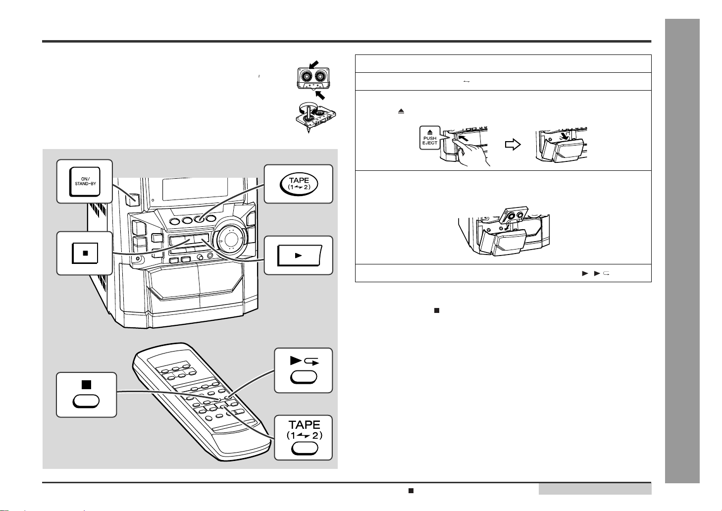
NO.
PRICE
RANK
DESCRIPTIONPARTS CODE
NO. PARTS CODE
PRICE
RANK
DESCRIPTION
CD-BK250W/CD-BK2600W/CD-BK270W
C111,112 VCEAZA1EW107M J AB 100 µF,25V,Electrolytic
C113,114 VCTYPA1EX333K J AA 0.033 µF,25V
C115,116 VCKYMN1HB561K J AA 560 pF,50V
C117,118 VCEAZA1EW476M J AB 47 µF,25V,Electrolytic
C119 VCKYPA1HB222K J AA 0.0022 µF,50V
C120 VCTYMN1CX222K J AA 0.0022 µF,16V
C121 VCTYMN1EF223Z J AA 0.022 µF,25V
C122 VCEAZA1HW335M J AB 3.3 µF,50V,Electrolytic
C123,124 VCKYMN1HB271K J AA 270 pF,50V
C125,126 VCEAZA1HW226M J AB 22 µF,50V,Electrolytic
C127,128 VCKZPA1HF223Z J AA 0.022 µF,50V
C129,130 VCTYMN1CX332K J AA 0.0033 µF,16V
C131,132 VCEAZA1EW476M J AB 47 µF,25V,Electrolytic
C133 VCEAZA1HW226M J AB 22 µF,50V,Electrolytic
C134 VCEAZA1AW227M J AC 220 µF,10V,Electrolytic
C135 VCTYMN1EF223Z J AA 0.022 µF,25V
C136 VCKZPA1HF223Z J AA 0.022 µF,50V
C137 VCQYKA1HM473K J AB 0.047 µF,50V,Mylar
C138 VCQPKA2AA822J J AA 0.0082 µF,100V,Polypropylene
C139 VCQYKA1HM393K J AB 0.039 µF,50V,Mylar
C140 VCEAZA1EW476M J AB 47 µF,25V,Electrolytic
C141 VCEAZA1CW107M J AC 100 µF,16V,Electrolytic
C150 VCEAZA1HW106M J AB 10 µF,50V,Electrolytic
C301 VCTYMN1CY103N J AA 0.01 µF,16V
C303 VCCCMN1HH100J J AA 10 pF (CH),50V
C304 VCTYMN1CY103N J AA 0.01 µF,16V
C305 VCCCMN1HH4R7C J AA 4.7 pF (CH),50V
C306 VCTYMN1EF223Z J AA 0.022 µF,25V
C307 VCEAZA1HW106M J AB 10 µF,50V,Electrolytic
C308 VCCCMN1HH4R7C J AA 4.7 pF (CH),50V
C309 VCKYMN1HB102K J AA 0.001 µF,50V
C310 VCCCMN1HH150J J AA 15 pF (CH),50V
C311 VCCSMN1HL180J J AA 18 pF,50V
C312 VCTYMN1EF223Z J AA 0.022 µF,25V
C313 VCCSMN1HL220J J AA 22 pF,50V
C314,315 VCTYMN1CX472K J AA 0.0047 µF,16V
C316 VCTYMN1EF223Z J AA 0.022 µF,25V
C317 VCKYMN1HB102K J AA 0.001 µF,50V
C318 VCKYMN1HB101K J AA 100 pF,50V
C323 VCTYMN1EF223Z J AA 0.022 µF,25V
C324 VCCUMN1HJ3R9K J AA 3.9 pF (UJ),50V
C330 VCCSMN1HL150J J AA 15 pF,50V
C331 VCKZPA1HF473Z J AA 0.047 µF,50V
C332 VCTYMN1EF223Z J AA 0.022 µF,25V
C334 VCCCMN1HH220J J AA 22 pF (CH),50V
C335 VCKYMN1HB561K J AA 560 pF,50V
C338 VCKYMN1HB102K J AA 0.001 µF,50V
C340 VCKYMN1HB102K J AA 0.001 µF,50V
C342 VCTYMN1EF223Z J AA 0.022 µF,25V
C350 VCKZPA1HF223Z J AA 0.022 µF,50V
C352 VCEAZA1HW106M J AB 10 µF,50V,Electrolytic
C353,354 VCTYMN1EF223Z J AA 0.022 µF,25V
C355 VCCSMN1HL220J J AA 22 pF,50V
C356 VCKYMN1HB102K J AA 0.001 µF,50V
C357 VCEAZA1HW225M J AB 2.2 µF,50V,Electrolytic
C358 VCEAZA1HW105M J AB 1 µF,50V,Electrolytic
C361 VCTYMN1EF223Z J AA 0.022 µF,25V
C362 VCEAZA1HW335M J AB 3.3 µF,50V,Electrolytic
C363 VCTYMN1EF223Z J AA 0.022 µF,25V
C364 VCEAZA1HW225M J AB 2.2 µF,50V,Electrolytic
C365 VCKZPA1HF223Z J AA 0.022 µF,50V
C366 VCKYMN1HB102K J AA 0.001 µF,50V
C367,368 VCEAZA1HW105M J AB 1 µF,50V,Electrolytic
C369 VCCSMN1HL270J J AA 27 pF,50V
C370~372 VCEAZA1HW105M J AB 1 µF,50V,Electrolytic
C373,374 VCTYPA1CX153K J AA 0.015 µF,16V
C380 VCEAZA1HW106M J AB 10 µF,50V,Electrolytic
C381 VCCCMN1HH120J J AA 12 pF (CH),50V
C382 VCCCMN1HH150J J AA 15 pF (CH),50V
C384 VCKYMN1HB102K J AA 0.001 µF,50V
C385 VCTYMN1CY103N J AA 0.01 µF,16V
C386 VCKYMN1HB331K J AA 330 pF,50V
C387 VCTYMN1EF223Z J AA 0.022 µF,25V
C388 VCKYMN1HB102K J AA 0.001 µF,50V
C389 VCTYMN1EF223Z J AA 0.022 µF,25V
C391 VCEAZA1EW476M J AB 47 µF,25V,Electrolytic
C392 VCKYMN1HB102K J AA 0.001 µF,50V
C393 VCEAZA1HW105M J AB 1 µF,50V,Electrolytic
C394 VCEAZA1EW476M J AB 47 µF,25V,Electrolytic
C395 VCTYMN1EF223Z J AA 0.022 µF,25V
C396 VCEAZA1AW107M J AB 100 µF,10V,Electrolytic
C397 VCTYMN1EF223Z J AA 0.022 µF,25V
C398 VCEAZA1AW107M J AB 100 µF,10V,Electrolytic
C399 VCTYMN1EF223Z J AA 0.022 µF,25V
C561 VCKYPA1HB271K J AA 270 pF,50V
C562 VCKYMN1HB271K J AA 270 pF,50V
C563 VCEAZA1HW225M J AB 2.2 µF,50V,Electrolytic
C564,565 VCTYMN1CX272K J AA 0.0027 µF,16V
C566 VCEAZA1HW225M J AB 2.2 µF,50V,Electrolytic
C567,568 VCTYMN1CX682K J AA 0.0068 µF,16V
C569 VCEAZA1HW225M J AB 2.2 µF,50V,Electrolytic
C570~572 VCTYMN1EF223Z J AA 0.022 µF,25V
C573 VCKZPA1HF223Z J AA 0.022 µF,50V
C601 VCEAZA1CW227M J AC 220 µF,16V,Electrolytic
C603 VCEAZA1HW226M J AB 22 µF,50V,Electrolytic
C605,606 VCFYDA1HA154J J AB 0.15 µF,50V,Polyester
C607,608 VCFYHA1HA104J J AB 0.1 µF,50V,Thin Film
C609,610 VCEAZA1HW105M J AB 1 µF,50V,Electrolytic
C611,612 VCTYMN1CX272K J AA 0.0027 µF,16V
C613,614 VCEAZA1HW105M J AB 1 µF,50V,Electrolytic
C615,616 VCEAZA1HW475M J AB 4.7 µF,50V,Electrolytic
C617~624 VCEAZA1HW105M J AB 1 µF,50V,Electrolytic
C625,626 VCTYMN1CX562K J AA 0.0056 µF,16V
C635~638 VCKYMN1HB102K J AA 0.001 µF,50V
C639 VCEAZA1HW105M J AB 1 µF,50V,Electrolytic
C640 VCEAZA1HW226M J AB 22 µF,50V,Electrolytic
C690,691 VCKYMN1HB391K J AA 390 pF,50V
C693 VCKYMN1HB102K J AA 0.001 µF,50V
C701 VCEAZA1HW105M J AB 1 µF,50V,Electrolytic
C702 VCEAZA1AW227M J AC 220 µF,10V,Electrolytic
C703 VCTYMN1EF223Z J AA 0.022 µF,25V
C704 VCCSMN1HL150J J AA 15 pF,50V
C705 VCCSMN1HL180J J AA 18 pF,50V
C706 VCEAZA1HW476M J AB 47 µF,50V,Electrolytic
C707 VCEAZA1HW105M J AB 1 µF,50V,Electrolytic
C712 VCEAZA1HW476M J AB 47 µF,50V,Electrolytic
C714 VCEAZA1HW335M J AB 3.3 µF,50V,Electrolytic
C715 VCTYMN1CY103N J AA 0.01 µF,16V
C716 VCTYMN1EF223Z J AA 0.022 µF,25V
C717 VCEAZA1HW476M J AB 47 µF,50V,Electrolytic
C734,735 VCCSPA1HL221J J AA 220 pF,50V
C901,902 VCQYKA1HM104K J AB 0.1 µF,50V,Mylar
C903,904 RC-EZ0063AWZZ J AM 2200 µF,63V,Electrolytic
C905,906 VCQYKA1HM104K J AB 0.1 µF,50V,Mylar
C907 VCEAZW1VW228M J AH 2200 µF,35V,Electrolytic
C908,909 VCEAZA1HW107M J AC 100 µF,50V,Electrolytic
C910 VCEAZA1HW227M J AC 220 µF,50V,Electrolytic
C911,912 VCEAZA1HW476M J AB 47 µF,50V,Electrolytic
C913 VCEAZA1VW107M J AC 100 µF,35V,Electrolytic
C915 VCKZPA1HF223Z J AA 0.022 µF,50V
C916 VCEAZA1HW226M J AB 22 µF,50V,Electrolytic
C918 VCQYKA1HM104K J AB 0.1 µF,50V,Mylar
C920 VCEAZA1EW476M J AB 47 µF,25V,Electrolytic
C921 VCQYKA1HM104K J AB 0.1 µF,50V,Mylar
C923 VCEAZA1EW476M J AB 47 µF,25V,Electrolytic
C930,931 VCEAZA1HW224M J AB 0.22 µF,50V,Electrolytic
C932,933 VCKYMN1HB102K J AA 0.001 µF,50V
C934,935 VCEAZA1HW475M J AB 4.7 µF,50V,Electrolytic
C936,937 VCCSMN1HL150J J AA 15 pF,50V
C938,939 VCKYMN1HB821K J AA 820 pF,50V
C940,941 VCEAZA1HW107M J AC 100 µF,50V,Electrolytic
C942 VCFYDA1HA224J J AB 0.22 µF,50V,Polyester
C945,946 VCEAZA1HW106M J AB 10 µF,50V,Electrolytic
C947 VCTYMN1EF223Z J AA 0.022 µF,25V
C948 VCKZPA1HF223Z J AA 0.022 µF,50V
C949 VCEAZA1HW476M J AB 47 µF,50V,Electrolytic
C952,953 VCQYKA1HM473K J AB 0.047 µF,50V,Mylar
C967 VCEAZA1HW476M J AB 47 µF,50V,Electrolytic
C968 VCEAZA1HW106M J AB 10 µF,50V,Electrolytic
C969 VCEAZA1HW335M J AB 3.3 µF,50V,Electrolytic
C970 VCEAZW1CW688M J AH 6800 µF,16V,Electrolytic
CK1 VCTYPA1CX103K J AA 0.01 µF,16V
CK2 VCFYHA1HA474J J AD 0.47 µF,50V,Thin Film
CK3 VCKYBT1HB102K J AA 0.001 µF,50V
CK6 VCFYDA1HA104J J AB 0.1 µF,50V,Thin Film
CK7 VCFYHA1HA474J J AD 0.47 µF,50V,Thin Film
CK8 RC-EZY475AF1H J AB 4.7 µF,50V,Electrolytic
CK9 RC-EZY225AF1H J AB 2.2 µF,50V,Electrolytic
CK10,11 VCFYDA1HA104J J AB 0.1 µF,50V,Thin Film
CK12 RC-EZY225AF1H J AB 2.2 µF,50V,Electrolytic
CK13 VCTYPA1CX472K J AA 0.0047 µF,16V
CK14 VCTYPA1CX102K J AA 0.001 µF,16V
CK15 VCFYDA1HA683J J AB 0.068 µF,50V,Polyester
CK16 VCFYHA1HA224J J AC 0.22 µF,50V,Thin Film
– 2 –
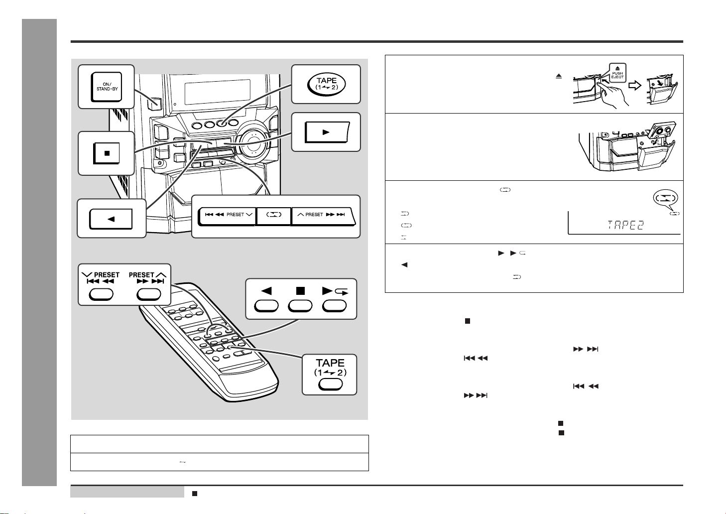
PRICE
RANK
DESCRIPTION
NO.
PARTS CODE
NO. PARTS CODE
PRICE
RANK
DESCRIPTION
CD-BK250W/CD-BK2600W/CD-BK270W
CK17 VCEAEA1AW227M J 220 µF,10V,Electrolytic
CK19 VCTYBT1EF223Z J AA 0.022 µF,25V
CK20 VCFYHA1HA224J J AC 0.22 µF,50V,Thin Film
CK21 VCFYDA1HA683J J AB 0.068 µF,50V,Polyester
CK22 VCTYPA1CX472K J AA 0.0047 µF,16V
CK23 VCKYPA1HB102K J AA 0.001 µF,50V
CK24~26 VCEAZA1HW225M J AB 2.2 µF,50V,Electrolytic
CK29,30 VCEAZA1HW225M J AB 2.2 µF,50V,Electrolytic
CK31 VCFYDA1HA154J J AB 0.15 µF,50V,Polyester
CK33~35 VCCSBT1HL470J J AA 47 pF,50V
CK41 VCEAZA1CW107M J AC 100 µF,16V,Electrolytic
CK42 VCTYBT1EF223Z J AA 0.022 µF,25V
CK43,44 VCEAZA1EW476M J AB 47 µF,25V,Electrolytic
CK45,46 RC-EZY225AF1H J AB 2.2 µF,50V,Electrolytic
CK47,48 VCCSPA1HL221J J AA 220 pF,50V
CK49,50 VCCSPA1HL101J J AA 100 pF,50V
CK51,52 VCEAZA1HW105M J AB 1 µF,50V,Electrolytic
CK53 VCEAZA1HW476M J AB 47 µF,50V,Electrolytic
CK72 VCEAZA1CW107M J AC 100 µF,16V,Electrolytic
CR1,2 VCEAZA1HW226M J AB 22 µF,50V,Electrolytic
CT1 VCKZPA1HF103Z J AA 0.01 µF,50V
RESISTORS
VRD-MN2BD000C J AA 0 ohm,Jumper,ø1.4×3.5mm,Ivory
R1,2 VRD-ST2CD123J J AA 12 kohms,1/6W
R3 VRD-ST2CD333J J AA 33 kohms,1/6W
R4,5 VRD-ST2CD123J J AA 12 kohms,1/6W
R6 VRD-ST2CD333J J AA 33 kohms,1/6W
R7 VRD-ST2CD470J J AA 47 ohms,1/6W
R9 VRD-ST2CD3R3J J AA 3.3 ohms,1/6W
R10 VRD-ST2CD273J J AA 27 kohms,1/6W
R11 VRD-MN2BD103J J AA 10 kohm,1/8W
R12 VRD-MN2BD331J J AA 330 ohms,1/8W
R13~17 VRD-MN2BD102J J AA 1 kohm,1/8W
R18 VRD-ST2CD102J J AA 1 kohm,1/6W
R19 VRD-ST2CD153J J AA 15 kohms,1/6W
R20 VRD-ST2CD103J J AA 10 kohm,1/6W
R22 VRD-ST2CD101J J AA 100 ohm,1/6W
R23 VRD-MN2BD221J J AA 220 ohms,1/8W
R24,25 VRD-MN2BD222J J AA 2.2 kohms,1/8W
R26,27 VRD-MN2BD103J J AA 10 kohm,1/8W
R28,29 VRD-ST2CD222J J AA 2.2 kohms,1/6W
R30 VRD-ST2CD822J J AA 8.2 kohms,1/6W
R31~38 VRD-ST2CD102J J AA 1 kohm,1/6W
R39,40 VRD-MN2BD681J J AA 680 ohms,1/8W
R41 VRD-MN2BD123J J AA 12 kohms,1/8W
R42 VRD-MN2BD122J J AA 1.2 kohms,1/8W
R43 VRD-MN2BD101J J AA 100 ohm,1/8W
R44 VRD-ST2CD123J J AA 12 kohms,1/6W
R45,46 VRD-MN2BD471J J AA 470 ohms,1/8W
R47 VRD-MN2BD101J J AA 100 ohm,1/8W
R49 VRD-ST2EE1R0J J AA 1 ohm,1/4W
R65 VRD-ST2CD332J J AA 3.3 kohms,1/6W
1 R80 VRG-ST2EG3R3J J AB 3.3 ohms,1/4W,Fusible
R101,102 VRD-MN2BD102J J AA 1 kohm,1/8W
R103,104 VRD-MN2BD222J J AA 2.2 kohms,1/8W
R105,106 VRD-MN2BD332J J AA 3.3 kohms,1/8W
R107,108 VRD-MN2BD473J J AA 47 kohms,1/8W
R109,110 VRD-MN2BD472J J AA 4.7 kohms,1/8W
R111 VRD-MN2BD153J J AA 15 kohms,1/8W
R112 VRD-ST2CD153J J AA 15 kohms,1/6W
R113,114 VRD-ST2CD102J J AA 1 kohm,1/6W
R115,116 VRD-ST2CD560J J AA 56 ohms,1/6W
R117,118 VRD-MN2BD104J J AA 100 kohm,1/8W
R119,120 VRD-MN2BD392J J AA 3.9 kohms,1/8W
R121,122 VRD-MN2BD333J J AA 33 kohms,1/8W
R123,124 VRD-MN2BD562J J AA 5.6 kohms,1/8W
R125 VRD-MN2BD683J J AA 68 kohms,1/8W
R126,127 VRD-MN2BD392J J AA 3.9 kohms,1/8W
R128,129 VRD-MN2BD682J J AA 6.8 kohms,1/8W
R130,131 VRD-MN2BD152J J AA 1.5 kohms,1/8W
R132,133 VRD-MN2BD101J J AA 100 ohm,1/8W
R134,135 VRD-MN2BD103J J AA 10 kohm,1/8W
R136,137 VRD-ST2CD224J J AA 220 kohms,1/6W
R138 VRD-MN2BD103J J AA 10 kohm,1/8W
R139 VRD-ST2CD103J J AA 10 kohm,1/6W
R140 VRD-MN2BD473J J AA 47 kohms,1/8W
R141 VRD-ST2CD472J J AA 4.7 kohms,1/6W
R142 VRD-ST2CD820J J AA 82 ohms,1/6W
R143 VRD-MN2BD473J J AA 47 kohms,1/8W
R144 VRD-MN2BD223J J AA 22 kohms,1/8W
R145 VRD-ST2CD4R7J J AA 4.7 ohms,1/6W
R146,147 VRD-MN2BD103J J AA 10 kohm,1/8W
R148 VRD-MN2BD472J J AA 4.7 kohms,1/8W
R149 VRD-ST2EE151J J AA 150 ohms,1/4W
R158 VRD-ST2EE221J J AA 220 ohms,1/4W
R302 VRD-MN2BD100J J AA 10 ohm,1/8W
R309 VRD-ST2CD103J J AA 10 kohm,1/6W
R311 VRD-MN2BD104J J AA 100 kohm,1/8W
R313 VRD-MN2BD333J J AA 33 kohms,1/8W
R314 VRD-ST2CD220J J AA 22 ohms,1/6W
R316 VRD-MN2BD472J J AA 4.7 kohms,1/8W
R322 VRD-MN2BD681J J AA 680 ohms,1/8W
R323 VRD-MN2BD683J J AA 68 kohms,1/8W
R325 VRD-MN2BD473J J AA 47 kohms,1/8W
R327 VRD-MN2BD330J J AA 33 ohms,1/8W
R336 VRD-MN2BD103J J AA 10 kohm,1/8W
R350 VRD-MN2BD272J J AA 2.7 kohms,1/8W
R351 VRD-MN2BD562J J AA 5.6 kohms,1/8W
R352 VRD-MN2BD102J J AA 1 kohm,1/8W
R353 VRD-MN2BD271J J AA 270 ohms,1/8W
R355 VRD-MN2BD332J J AA 3.3 kohms,1/8W
R356 VRD-MN2BD102J J AA 1 kohm,1/8W
R357 VRD-ST2CD474J J AA 470 kohms,1/6W
R358 VRD-ST2CD392J J AA 3.9 kohms,1/6W
R359 VRD-MN2BD182J J AA 1.8 kohms,1/8W
R360 VRD-MN2BD472J J AA 4.7 kohms,1/8W
R361,362 VRD-MN2BD153J J AA 15 kohms,1/8W
R363,364 VRD-MN2BD123J J AA 12 kohms,1/8W
R365 VRD-MN2BD103J J AA 10 kohm,1/8W
R372~374 VRD-MN2BD102J J AA 1 kohm,1/8W
R375 VRD-ST2CD471J J AA 470 ohms,1/6W
R376 VRD-MN2BD102J J AA 1 kohm,1/8W
R377 VRD-MN2BD473J J AA 47 kohms,1/8W
R378 VRD-MN2BD102J J AA 1 kohm,1/8W
R379 VRD-MN2BD222J J AA 2.2 kohms,1/8W
R380 VRD-MN2BD152J J AA 1.5 kohms,1/8W
R381 VRD-MN2BD103J J AA 10 kohm,1/8W
R382 VRD-ST2EE151J J AA 150 ohms,1/4W
R383 VRD-MN2BD562J J AA 5.6 kohms,1/8W
R384 VRD-ST2CD562J J AA 5.6 kohms,1/6W
R385 VRD-MN2BD562J J AA 5.6 kohms,1/8W
R386 VRD-ST2CD223J J AA 22 kohms,1/6W
R387 VRD-ST2CD562J J AA 5.6 kohms,1/6W
R388 VRD-MN2BD392J J AA 3.9 kohms,1/8W
R391,392 VRD-ST2EE271J J AA 270 ohms,1/4W
R393 VRD-MN2BD102J J AA 1 kohm,1/8W
R395 VRD-MN2BD473J J AA 47 kohms,1/8W
R561 VRD-MN2BD103J J AA 10 kohm,1/8W
R562 VRD-MN2BD824J J AA 820 kohms,1/8W
R563 VRD-ST2EE271J J AA 270 ohms,1/4W
R565 VRD-MN2BD333J J AA 33 kohms,1/8W
R566 VRD-ST2CD224J J AA 220 kohms,1/6W
R567 VRD-MN2BD683J J AA 68 kohms,1/8W
R568 VRD-MN2BD224J J AA 220 kohms,1/8W
R569 VRD-MN2BD104J J AA 100 kohm,1/8W
R570 VRD-ST2CD123J J AA 12 kohms,1/6W
R571 VRD-MN2BD394J J AA 390 kohms,1/8W
R572 VRD-MN2BD104J J AA 100 kohm,1/8W
R573 VRD-MN2BD563J J AA 56 kohms,1/8W
R574 VRD-MN2BD105J J AA 1 Mohm,1/8W
R575 VRD-MN2BD474J J AA 470 kohms,1/8W
R576 VRD-MN2BD225J J AA 2.2 Mohms,1/8W
R577 VRD-MN2BD154J J AA 150 kohms,1/8W
R578 VRD-MN2BD104J J AA 100 kohm,1/8W
R579 VRD-ST2CD153J J AA 15 kohms,1/6W
R580 VRD-MN2BD184J J AA 180 kohms,1/8W
R601~603 VRD-ST2CD102J J AA 1 kohm,1/6W
R604,605 VRD-MN2BD103J J AA 10 kohm,1/8W
R606,607 VRD-MN2BD392J J AA 3.9 kohms,1/8W
R608,609 VRD-MN2BD122J J AA 1.2 kohms,1/8W
R610,611 VRD-MN2BD222J J AA 2.2 kohms,1/8W
R612,613 VRD-MN2BD391J J AA 390 ohms,1/8W
R614,615 VRD-MN2BD332J J AA 3.3 kohms,1/8W
R616 VRD-ST2CD222J J AA 2.2 kohms,1/6W
R617 VRD-MN2BD222J J AA 2.2 kohms,1/8W
R618,619 VRD-ST2CD331J J AA 330 ohms,1/6W
R620,621 VRD-MN2BD223J J AA 22 kohms,1/8W
R622,623 VRD-MN2BD224J J AA 220 kohms,1/8W
R690,691 VRD-MN2BD682J J AA 6.8 kohms,1/8W
R692,693 VRD-MN2BD333J J AA 33 kohms,1/8W
R702~704 VRD-ST2CD102J J AA 1 kohm,1/6W
R705~707 VRD-MN2BD102J J AA 1 kohm,1/8W
– 3 –

NO.
PRICE
RANK
DESCRIPTIONPARTS CODE
NO. PARTS CODE
PRICE
RANK
DESCRIPTION
CD-BK250W/CD-BK2600W/CD-BK270W
R708~712 VRD-ST2CD102J J AA 1 kohm,1/6W
R713~717 VRD-MN2BD102J J AA 1 kohm,1/8W
R718~721 VRD-ST2CD102J J AA 1 kohm,1/6W
R724,725 VRD-ST2CD102J J AA 1 kohm,1/6W
R726~728 VRD-ST2CD222J J AA 2.2 kohms,1/6W
R729 VRD-ST2CD102J J AA 1 kohm,1/6W
R731 VRD-MN2BD103J J AA 10 kohm,1/8W
R732,733 VRD-MN2BD102J J AA 1 kohm,1/8W
R734~736 VRD-ST2CD102J J AA 1 kohm,1/6W
R738 VRD-ST2CD223J J AA 22 kohms,1/6W
R739,740 VRD-ST2CD102J J AA 1 kohm,1/6W
R741 VRD-MN2BD102J J AA 1 kohm,1/8W
R746~748 VRD-MN2BD102J J AA 1 kohm,1/8W
R749~751 VRD-MN2BD104J J AA 100 kohm,1/8W
R752 VRD-MN2BD330J J AA 33 ohms,1/8W
R753 VRD-MN2BD102J J AA 1 kohm,1/8W
R754 VRD-MN2BD103J J AA 10 kohm,1/8W
R755 VRD-MN2BD102J J AA 1 kohm,1/8W
R756 VRD-MN2BD103J J AA 10 kohm,1/8W
R758~760 VRD-MN2BD103J J AA 10 kohm,1/8W
R761 VRD-MN2BD103J J AA 10 kohm,1/8W
R765 VRD-ST2CD472J J AA 4.7 kohms,1/6W
R766~768 VRD-MN2BD103J J AA 10 kohm,1/8W
R769 VRD-ST2CD102J J AA 1 kohm,1/6W
R770 VRD-ST2CD103J J AA 10 kohm,1/6W
R771 VRD-MN2BD103J J AA 10 kohm,1/8W
R772 VRD-ST2CD103J J AA 10 kohm,1/6W
R773 VRD-ST2CD102J J AA 1 kohm,1/6W
R774 VRD-MN2BD103J J AA 10 kohm,1/8W
R777~779 VRD-MN2BD103J J AA 10 kohm,1/8W
R781 VRD-MN2BD473J J AA 47 kohms,1/8W
R782 VRD-MN2BD104J J AA 100 kohm,1/8W
R783 VRD-MN2BD101J J AA 100 ohm,1/8W
R901,902 VRD-ST2CD223J J AA 22 kohms,1/6W
R903 VRD-RT2HD332J J AA 3.3 kohms,1/2W
R904 VRD-ST2CD222J J AA 2.2 kohms,1/6W
R905 VRD-ST2CD473J J AA 47 kohms,1/6W
R906 VRD-ST2CD100J J AA 10 ohm,1/6W
R907 VRD-ST2CD123J J AA 12 kohms,1/6W
R908 VRD-ST2EE561J J AA 560 ohms,1/4W
R909 VRD-ST2CD223J J AA 22 kohms,1/6W
R930 VRD-ST2CD104J J AA 100 kohm,1/6W
R931 VRD-MN2BD104J J AA 100 kohm,1/8W
R932,933 VRD-MN2BD563J J AA 56 kohms,1/8W
R934 VRD-MN2BD102J J AA 1 kohm,1/8W
R935 VRD-ST2CD102J J AA 1 kohm,1/6W
R936,937 VRD-MN2BD821J J AA 820 ohms,1/8W
R938,939 VRD-MN2BD563J J AA 56 kohms,1/8W
R940,941 VRD-MN2BD102J J AA 1 kohm,1/8W
R942 VRD-MN2BD223J J AA 22 kohms,1/8W
1 R943,944 VRG-ST2EC101J J AB 100 ohm,1/4W,Fusible
R945~948 VRN-VV3DAR22J J AC 0.22 ohms,2W
R949,950 VRN-VV3AAR10J J AB 0.1 ohm,1W
R951 VRD-MN2BD102J J AA 1 kohm,1/8W
R952 VRD-ST2CD102J J AA 1 kohm,1/6W
R953 VRD-MN2BD152J J AA 1.5 kohms,1/8W
R954 VRD-ST2CD152J J AA 1.5 kohms,1/6W
R955~957 VRD-MN2BD563J J AA 56 kohms,1/8W
R958,959 VRD-ST2EE4R7J J AA 4.7 ohms,1/4W
R967,968 VRD-ST2CD472J J AA 4.7 kohms,1/6W
R969 VRD-RT2HD4R7J J AA 4.7 ohms,1/2W
R970 VRD-RT2HD102J J AA 1 kohm,1/2W
R971 VRD-ST2CD683J J AA 68 kohms,1/6W
R972 VRD-ST2CD153J J AA 15 kohms,1/6W
R973 VRD-ST2CD473J J AA 47 kohms,1/6W
R977,978 VRD-ST2EE470J J AA 47 ohms,1/4W
R981,982 VRD-RT2HD681J J AA 680 ohms,1/2W
R983 VRD-ST2CD224J J AA 220 kohms,1/6W
R984 VRD-ST2CD473J J AA 47 kohms,1/6W
R986 VRD-RT2HD681J J AA 680 ohms,1/2W
R988 VRD-RT2HD681J J AA 680 ohms,1/2W
RD01 VRD-MN2BD681J J AA 680 ohms,1/8W
RD02 VRD-MN2BD821J J AA 820 ohms,1/8W
RD03 VRD-ST2CD102J J AA 1 kohm,1/6W
RD04 VRD-MN2BD152J J AA 1.5 kohms,1/8W
RD05 VRD-MN2BD222J J AA 2.2 kohms,1/8W
RD06 VRD-MN2BD272J J AA 2.7 kohms,1/8W
RD07 VRD-MN2BD392J J AA 3.9 kohms,1/8W
RD08 VRD-ST2CD562J J AA 5.6 kohms,1/6W
RD09 VRD-MN2BD103J J AA 10 kohm,1/8W
RD10 VRD-MN2BD183J J AA 18 kohms,1/8W
RD11 VRD-MN2BD333J J AA 33 kohms,1/8W
RD12 VRD-MN2BD104J J AA 100 kohm,1/8W
RD13 VRD-MN2BD681J J AA 680 ohms,1/8W
RD14 VRD-MN2BD821J J AA 820 ohms,1/8W
RD15 VRD-ST2CD182J J AA 1.8 kohms,1/6W
RD16 VRD-ST2CD392J J AA 3.9 kohms,1/6W
RD17 VRD-MN2BD184J J AA 180 kohms,1/8W
RD18 VRD-MN2BD681J J AA 680 ohms,1/8W
RD19 VRD-ST2CD821J J AA 820 ohms,1/6W
RD20 VRD-MN2BD102J J AA 1 kohm,1/8W
RD21 VRD-MN2BD152J J AA 1.5 kohms,1/8W
RD22 VRD-MN2BD222J J AA 2.2 kohms,1/8W
RD23 VRD-MN2BD272J J AA 2.7 kohms,1/8W
RD24 VRD-MN2BD392J J AA 3.9 kohms,1/8W
RD25 VRD-MN2BD562J J AA 5.6 kohms,1/8W
RD26 VRD-ST2CD103J J AA 10 kohm,1/6W
RD27 VRD-MN2BD183J J AA 18 kohms,1/8W
RD28 VRD-ST2CD333J J AA 33 kohms,1/6W
RD29 VRD-MN2BD104J J AA 100 kohm,1/8W
RD30 VRD-MN2BD562J J AA 5.6 kohms,1/8W
RK1 VRD-ST2CD103J J AA 10 kohm,1/6W
RK2,3 VRD-ST2CD563J J AA 56 kohms,1/6W
RK4 VRD-ST2CD103J J AA 10 kohm,1/6W
RK5 VRD-ST2CD102J J AA 1 kohm,1/6W
RK7 VRD-ST2CD102J J AA 1 kohm,1/6W
RK8 VRD-ST2CD562J J AA 5.6 kohms,1/6W
RK9~11 VRD-ST2CD102J J AA 1 kohm,1/6W
RK12 VRD-ST2CD101J J AA 100 ohm,1/6W
RK13 VRD-ST2CD122J J AA 1.2 kohms,1/6W
RK14,15 VRD-RT2HD101J J AA 100 ohm,1/2W
RK36,37 VRD-ST2CD391J J AA 390 ohms,1/6W
RK38 VRD-ST2CD101J J AA 100 ohm,1/6W
RK39,40 VRD-ST2CD102J J AA 1 kohm,1/6W
RK41,42 VRD-ST2CD103J J AA 10 kohm,1/6W
RK43 VRD-ST2CD183J J AA 18 kohms,1/6W
RK44,45 VRD-ST2CD682J J AA 6.8 kohms,1/6W
RK46 VRD-ST2CD183J J AA 18 kohms,1/6W
RK47 VRD-ST2CD822J J AA 8.2 kohms,1/6W
RK48 VRD-ST2CD103J J AA 10 kohm,1/6W
RK49,50 VRD-ST2CD103J J AA 10 kohm,1/6W
OTHER CIRCUITRY PARTS
BI4/CNS4 QCNWN1572AWZZ J AF Connector Ass’y,6/6Pin
BI102/CNS102 QCNWN1974AWZZ J Connector Ass’y,7/6Pin
BI601/CNS601 QCNWN1842AWZZ J AG Connector Ass’y,6/6Pin
BI701/CNS8 QCNWN1843AWZZ J AH Connector Ass’y,9/9Pin
BI902/CNS902 QCNWN1875AWZZ J AH Connector Ass’y,10/10Pin
BI903/CNS903 QCNWN2028AWZZ J Connector Ass’y,3/3Pin
[CD-BK270W Only]
BIK1/CNSK1 QCNWN1876AWZZ J Connector Ass’y,10/10Pin
CNP1 QCNCM704GAWZZ J AC Plug,7Pin
CNP2 QCNCM704HAWZZ J AC Plug,8Pin
CNP3 92LCONE6P53253 J AC Plug,6Pin
CNP4 QCNCM705FAFZZ J AB Plug,6Pin
CNP7 92LCONE6P53254 J AC Plug,6Pin
CNP8 92LCONE9P53254 J AD Plug,9Pin
CNP101 QCNCM705CAFZZ J AA Plug,3Pin
CNP301 92LCONE2P5268 J AB Plug,2Pin
CNP701 QCNCWZX32AWZZ J Socket,32Pin
CNP902 92LCONEAP5267 J AC Plug,10Pin
CNP971 92LCONE2P53253 J AB Plug,2Pin
CNP981 92LCONE5P52287 J AC Plug,5Pin
CNPK1 QCNCM705KAWZZ J AC Plug,10Pin
CNR1 92LCONE3P53253 J AB Plug,3Pin [CD-BK270W Only]
CNS1A/B QCNWN1537AWZZ J AG Connector Ass’y,7/7Pin
CNS2A/B QCNWN1538AWZZ J AG Connector Ass’y,8/8Pin
CNS3A/B QCNWN1539AWZZ J AE Connector Ass’y,6/6Pin
CNS701 QCNCWZF32AWZZ J Socket,32Pin
CNS702 QCNCWZY10AWZZ J Socket,10Pin
CNS971 QCNWN1389AWZZ J AC Connector Ass’y,2Pin
1 F901,902 QFS-D402CAWNI J AC Fuse,T4A L 250V
1 F903,904 QFS-D202CAWNI J AC Fuse,T2A L 250V
FFC701 QCNWN1878AWZZ J Flat Cable,32Pin
FFC702 QCNWN1845AWZZ J Flat Cable,10Pin
FL701 VVKBJ749GNK-1 J BD FL Display
FW981 QCNWN1836AWZZ J AD Flat Wire,5Pin
JK1 QJAKJ0007AWZZ J AF Jack,Mic
JK690 QSOCJ0219AWZZ J AD Jack,Video/AUX In
JK701 QJAKM0004AWZZ J AK Jack,Headphones
LG1 QLUGP0001AWZZ J AC Lug
1 LUG1,2 92LLUG1746A J AA Lug
M1 92LMTR2790CASY J BB Motor with Chassis [Spindle]
M2 92LMTR1854BASY J AP Motor with Gear [Sled]
– 4 –
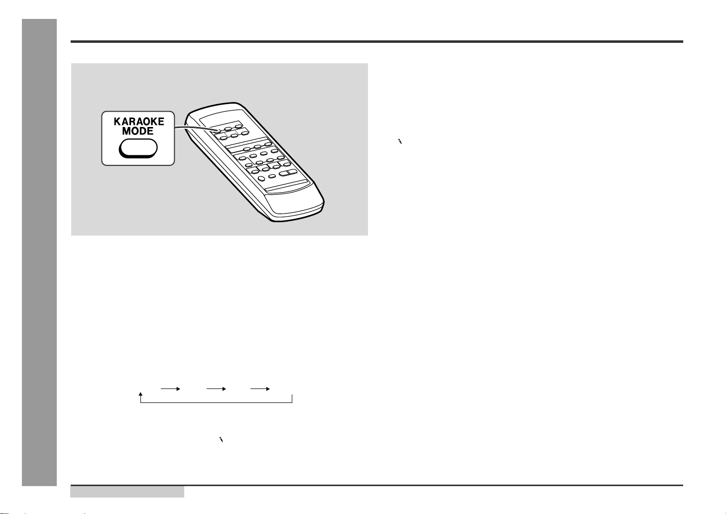
PRICE
RANK
DESCRIPTION
NO.
PARTS CODE
NO. PARTS CODE
PRICE
RANK
DESCRIPTION
CD-BK250W/CD-BK2600W/CD-BK270W
M3 92LTWMEN7E6Y J AR Motor with Worm Pulley
[T/T Up Down Loading]
M901 RMOTV0027AWZZ J AM Motor,Air Cooling Fan
PINK1 QLUGP0002AWZZ J AB Lug
RL914 RRLYD0016AWZZ J AH Relay
RX701 VHLN63H380A-1 J AK Remote Sensor,N63H380A
SO302 QTANC0206AWZZ J AD FM Antenna Terminal
SO901 QTANA0417AWZZ J AE Terminal,Speaker
SR1 QTANA0420AWZZ J Terminal,Surround Speaker
[CD-BK270W Only]
SW1 SWMPU10780MLB J AH Switch,Push Type [Open/Close]
SW2 SWMPU11470MLB J AE Switch,Push Type [Clamp]
SW3 SWMPU11470MLB J AE Switch,Push Type [Disc Number]
SW4 QSWF9001AW01 J AD Switch,Push Type [Pickup In]
SW601 QSW-S0024AWZZ J AE Switch,Slide Type
[Span Selector]
SW701 92LSWICHT1663T J AC Switch,Key Type [On/Stand-by]
SW702 92LSWICHT1663T J AC Switch,Key Type [Clock]
SW703 92LSWICHT1663T J AC Switch,Key Type [Timer/Sleep]
SW712 92LSWICHT1663T J AC Switch,Key Type [Disc Skip]
SW713 92LSWICHT1663T J AC Switch,Key Type [Open/Close]
SW714 92LSWICHT1663T J AC Switch,Key Type [Dimmer]
SW715 92LSWICHT1663T J AC Switch,Key Type [X-Bass/Demo]
SW716 92LSWICHT1663T J AC Switch,Key Type [Equalizer]
SW717 92LSWICHT1663T J AC Switch,Key Type [Volume Up]
SW718 92LSWICHT1663T J AC Switch,Key Type [Volume Down]
SW719 92LSWICHT1663T J AC Switch,Key Type
[Reverse Mode]
SW720 92LSWICHT1663T J AC Switch,Key Type [CD]
SW721 92LSWICHT1663T J AC Switch,Key Type [Tape]
SW722 92LSWICHT1663T J AC Switch,Key Type [Tuning Down]
SW723 92LSWICHT1663T J AC Switch,Key Type [Memory/Set]
SW724 92LSWICHT1663T J AC Switch,Key Type [Rewind]
SW725 92LSWICHT1663T J AC Switch,Key Type [Fast forward]
SW726 92LSWICHT1663T J AC Switch,Key Type [Play]
SW727 92LSWICHT1663T J AC Switch,Key Type [Stop]
SW728 92LSWICHT1663T J AC Switch,Key Type [Reverse Play]
SW729 92LSWICHT1663T J AC Switch,Key Type [Rec/Pause]
SW730 92LSWICHT1663T J AC Switch,Key Type [Tuning Up]
SW731 92LSWICHT1663T J AC Switch,Key Type [Video/Aux]
SW732 92LSWICHT1663T J AC Switch,Key Type [Tuner (Band)]
1 SW801 QSOCE0009AWZZ J AH Switch,Slide Type
[Voltage Selector]
CD MECHANISM PARTS
301 NGERH0011AWZZ J AC Gear,Middle
302 NGERH0012AWZZ J AC Gear,Drive
303 MLEVP0080AWZZ J AC Rail,Guide
304 NSFTM0020AWFW J AD Shaft,Guide
305 92LM-CUSN1524A J AC Cushion
1 306 92LHPC1LXASY J BD Pickup Unit Ass’y
306- 1 ———— — Pickup Unit
(Not Replacement Item)
306- 2 NGERR0043AFZZ J AC Gear,Rack
306- 3 MSPRC0961AFZZ J AA Spring,Rack
701 XBSSD26P06000 J AA Screw,ø2.6×6mm
702 XHBSD20P05000 J AA Screw,ø2×5mm
703 XBBSD20P03000 J AA Screw,ø2×3mm
704 LX-WZ1070AFZZ J AA Washer,ø1.5×3.8×0.25mm
M1 92LMTR2790CASY J BB Motor with Chassis [Spindle]
M2 92LMTR1854BASY J AP Motor with Gear [Sled]
SW4 QSW-F9001AW01 J AD Switch,Leaf Type [Pickup In]
CABINET PARTS
201 92LCAB3563AASY J Front Panel Ass’y
[For CD-BK250W]
201 92LCAB3567AASY J Front Panel Ass’y
[For CD-BK2600W]
201 92LCAB3747AASY J Front Panel Ass’y
[For CD-BK270W]
201- 1 ———— — Front Panel
(Not Replacement Item)
201- 2 GDORF0099AWSA J AE Holder,Cassette [Tape 1]
201- 3 GDORF0100AWSA J AE Holder,Cassette [Tape 2]
201- 4 GCOVA1349AWSA J AG Cover,Cassette [Tape 1]
[For CD-BK250W/CD-BK270W]
201- 4 GCOVA1349AWSB J AH Cover,Cassette [Tape 1]
[For CD-BK2600W]
201- 5 GCOVA1388AWSA J Cover,Cassette [Tape 2]
[For CD-BK250W/CD-BK270W]
201- 5 GCOVA1388AWSB J Cover,Cassette [Tape 2]
[For CD-BK2600W]
201- 6 HDECQ0686AWSA J AE Panel,Cassette [Tape 1]
201- 7 HDECQ0687AWSA J AE Panel,Cassette [Tape 2]
201- 8 HDECQ0748AWSA J Panel,Amp. [For CD-BK250W]
201- 8 HDECQ0749AWSA J Panel,Amp. [For CD-BK2600W]
201- 8 HDECQ0775AWSA J Panel,Amp. [For CD-BK270W]
201- 9 JKNBZ0808AWSA J AE Button,Power
[For CD-BK250W/CD-BK270W]
201- 9 JKNBZ0808AWSB J AE Button,Power
[For CD-BK2600W]
201-10 JKNBZ0778AWSA J AF Button,Dimmer/Tuning
[For CD-BK250W/CD-BK270W]
201-10 JKNBZ0778AWSB J AG Button,Dimmer/Tuning
[For CD-BK2600W]
201-11 JKNBZ0779AWSA J AF Button,Function
201-12 HDECQ0690AWSA J AC Volume Ring
201-13 JKNBZ0780AWSA J AF Button,Disc Control
[For CD-BK250W/CD-BK270W]
201-13 JKNBZ0780AWSB J AF Button,Disc Control
[For CD-BK2600W]
201-14 JKNBZ0804AWSA J Button,Center Operation
201-15 GCOVA1351AWSA J AB Cover,Operation LED A
201-16 MLIFP0008AWZZ J AD Damper
201-17 MSPRD0092AWFJ J AB Spring,Cassette [Tape 1]
201-18 MSPRD0093AWFJ J AB Spring,Cassette [Tape 2]
201-19 JKNBZ0783AWSA J AF Button,X-Bass/Equalizer
201-20 PSHEP0063AWZZ J AB Filter,Remote Sensor
201-21 LHLDZ1328AWZZ J AC Holder,Cassette Lock
201-22 MSPRC0029AWFJ J AB Spring,Cassette Lock
201-23 MLOKC0006AWZZ J AB Lock Lever Cassette [Tape 1]
201-24 MLOKC0007AWZZ J AB Lock Lever Cassette [Tape 2]
201-25 JKNBZ0805AWSA J AE Button,Volume
201-26 92LBADGE1671A J AC Badge,SHARP
202 92LCAB3561BASY J AN Side Panel Ass’y,Left
[For CD-BK250W/CD-BK270W]
202 92LCAB3565BASY J AN Side Panel Ass’y Left
[For CD-BK2600W]
202- 1 ———— — Side Panel,Left
(Not Replacement Item)
202- 2 PCUSG0022AWZZ J AB Cushion,Leg
203 92LCAB3561CASY J AN Side Panel Ass’y,Right
[For CD-BK250W/CD-BK270W]
203 92LCAB3565CASY J AN Side Panel Ass’y Right
[For CD-BK2600W]
203- 1 ———— — Side Panel,Right
(Not Replacement Item)
203- 2 PCUSG0022AWZZ J AB Cushion,Leg
204 GCAB-1194AWSA J AP Cabinet,Top
[For CD-BK250W/CD-BK270W]
204 GCAB-1194AWSB J AP Cabinet,Top [For CD-BK2600W]
205 JKNBK0012AWSG J AK Knob,Karaoke
206 GCOVA1348AWSA J AH Cover,CD Tray
207 GITAR0736AWSA J Rear Panel [For CD-BK250W]
207 GITAR0737AWSA J Rear Panel [For CD-BK2600W]
207 GITAR0784AWSA J Rear Panel [For CD-BK270W]
211 LANGK0252AWFW J AE Bracket,Fan Support
212 LBSHC0002AWZZ J AD Bushing,AC Power Supply Cord
213 LCHSM0122AWFW J AN Chassis,Main
214 LHLDZ1332AWZZ J AD Holder,FL Display
215 TSPC-0887AWZZ J Label,Specifications
[CD-BK250W for Taiwan]
215 TSPC-0888AWZZ J Label,Specifications
[CD-BK250W for Thailand]
215 TSPC-0889AWZZ J Label,Specifications
[CD-BK250W Except for
Taiwan/Thailand]
215 TSPC-0893AWZZ J Label,Specifications
[CD-BK2600W for Taiwan]
215 TSPC-0894AWZZ J Label,Specifications
[CD-BK2600W for Thailand]
215 TSPC-0895AWZZ J Label,Specifications
[CD-BK2600W Except for
Taiwan/Thailand]
215 TSPC-0943AWZZ J Label,Specifications
[CD-BK270W for Taiwan]
215 TSPC-0944AWZZ J Label,Specifications
[CD-BK270W for Thailand]
215 TSPC-0945AWZZ J Label,Specifications
[CD-BK270W Except for
Taiwan/Thailand]
218 NFANP0001AWZZ J AD Rotary Fan
219 PCUSG0022AWZZ J AB Cushion,Leg
220 PRDAR0188AWFW J AR Heat Sink,Main
1 222 QACCA0003AW00 J AL AC Power Supply Cord
– 5 –

NO.
PRICE
RANK
DESCRIPTIONPARTS CODE
NO. PARTS CODE
PRICE
RANK
DESCRIPTION
CD-BK250W/CD-BK2600W/CD-BK270W
1 222 QACCE0010AW00 J AK AC Power Supply Cord
1 222 QACCJ0007AW00 J AK AC Power Supply Cord
1 222 QACCL0005AW00 J AN AC Power Supply Cord
223 QCNWN1844AWZZ J AC Lug Wire
1 224 QFSHD0001AWZZ J AB Holder,Fuse
225 92LBE231616 J AD Belt
226 92LCSPR1431C J AA Spring,Ring
227 92LEVA0330702 J AD Velvet Carpet,Chassis
228 92LMAG0104302 J AE Magnet
229 92LMT0304302 J AB Plate,Metal
230 92LNBAND1318A J AA Nylon Band,80mm
231 92LNM0305401 J AB Velvet Carpet
232 92LPT0303002 J AB Roller
233 92LPT0304303 J AB Lever,Stop
234 92LPT0304304 J AB Stopper
235 92LPT0304305 J AE Lever,Lock
236 92LPT0304306 J AG Stabilizer
237 92LPT0304307 J AC Support,Cam
238 92LPT0304308 J AB Lock Gear Pin
239 92LPT0304309 J AB Cap,Pulley Stopper
240 92LPT0305413 J AG Cam Gear Lower
241 92LPT0309506 J AD Gear,Turntable Drive
242 92LPT0309507 J AD Gear,Open/Close Drive
243 92LPT0309508 J AD Gear,Planet
244 92LPT0309509 J AD Gear,Drive
245 92LPT0309510 J AE Gear,Pulley
246 92LPT0309511 J AD Gear,Middle
247 92LPT0311101 J AB Lever,Clamp
248 92LPT0311102 J AC Lever,Disc
249 92LPT0312005 J AL Gear,Cam
250 92LPT0320201 J AE Support,Stabilizer
251 92LPT0330301 J AU Chassis,Loading
252 92LPT0330803 J AK CD,Chassis
253 92LPT0331003 J AT Chassis,Slide
254 92LPT0331105 J AM Turntable
255 92LSP0304303 J AB Spring,Stopper
256 92LSP0304305 J AB Spring,Lock
257 92LSP0304306 J AB Spring,Lock Gear
258 KMECB0018AWZZ J BE Tape Mechanism Ass’y
258- 1 92PF513-853 J BL Head Plate Block [Tape 2]
258- 2 92PF525-336 J Motor with Pulley [Tape]
258- 3 92PF567-677 J Tape Mechanism PWB Ass’y
258- 4 92PFF19N-21 J Belt,Main [Tape 2]
258- 5 92PF514-133 J AL Pinch Roller
258- 6 92PF19S-31 J Belt,FF/REW [Tape 2]
258- 7 92PFF19N-11 J Belt,Main [Tape 1]
258- 8 92PF522-061 J Clutch Ass’y Block [Tape 1]
258- 9 92PFF19S-52 J Belt,FF/REW [Tape 1]
258-10 92PF513-861 J Head Plate Block [Tape 1]
258-11 92PF522-063 J Clutch Ass’y Block [Tape 2]
259 PCOVQ3002AWZZ J AL Fan Cover
260 92LCAUT1706B J AA Label,Laser
261 92LCAUT1706A1 J AC Label,Class 3
262 LANGK0287AWFW J AC Bracket, Transformer Support
601 LX-BZ2222AXZZ J AB Screw,Special
602 XJBSD30P12000 J AA Screw,ø3×12mm
603 LX-JZ0010AFFD J AA Screw,ø3×10mm
604 XEBSD26P08000 J AA Screw,ø2.6×8mm
605 XBBSD20P04000 J AA Screw,ø2×4mm
606 XEBSD30P10000 J AA Screw,ø3×10mm
607 XEBSD30P12000 J AA Screw,ø3×12mm
608 XESSD30P10000 J AA Screw,ø3×10mm
610 XJBSD30P10000 J AA Screw,ø3×10mm
611 XJBSD30P14000 J AA Screw,ø3×14mm
613 XJSSD30P10000 J AA Screw,ø3×10mm
614 92LSC0308MBZI J AB Screw,ø3×8mm
615 92LSC0308RBZI J AB Screw,ø3×8mm
616 XHBSD40P08000 J AA Screw,ø4×8mm
ACCESSORIES/PACKING PARTS
QANTL0008AWZZ J AH AM Loop Antenna
1 QPLGA0003AWZZ J AF Adaptor,AC Plug
1 QPLGA0004AWZZ J AF Adaptor,AC Plug
SPAKA0300AWZZ J AM Packing Add.
SPAKC1145AWZZ J Packing Case
[CD-BK250W Except for
Australia/New Zealand]
SPAKC1237AWZZ J Packing Case
[CD-BK250W for Australia/New
Zealand]
SPAKC1238AWZZ J Packing Case
[CD-BK250W for Australia/New
Zealand]
SPAKC1239AWZZ J Packing Case
[CD-BK2600W Except for
Australia/New Zealand]
SPAKC1258AWZZ J Packing Case
[CD-BK270W for Australia/New
Zealand]
SPAKC1259AWZZ J Packing Case
[CD-BK270W Except for
Australia/New Zealand]
SPAKP0013AWZZ J AC Polyethylene Bag,Unit
SPAKZ0771AWZZ J AF Center Pad
SPAKZ0773AWZZ J AE Top Pad
SSAKA0007AWZZ J AB Polyethylene Bag,Accessories
TCAUA0061AWZZ J Caution Tag [For Taiwan Only]
TGANE0011AW70 J Warranty Card
[CD-BK250W for Philippines]
TGANE0011AW71 J Warranty Card
[CD-BK2600W for Philippines]
TGANE0011AW76 J Warranty Card
[CD-BK270W for Philippines]
TGANZ0028AW74 J Warranty Card
[CD-BK250W for Taiwan]
TGANZ0028AW75 J Warranty Card
[CD-BK2600W for Taiwan]
TGANZ0028AW82 J Warranty Card
[CD-BK270W for Taiwan]
TINST0096AWZZ J Operation Manual
[CD-BK250W/CD-BK2600W for
Thailand]
TINST0100AWZZ J Operation Manual
[CD-BK270W for Thailand]
TINSZ0691AWZZ J Operation Manual
[CD-BK250W/CD-BK2600W
Except for Thailand/Australia/
New Zealand]
TINSZ0692AWZZ J Operation Manual
[CD-BK250W/CD-BK2600W for
Australia/New Zealand]
TINSZ0714AWZZ J Operation Manual
[CD-BK270W Except for
Thailand/Australia/New Zealand]
TINSZ0715AWZZ J Operation Manual
[CD-BK270W for Australia/New
Zealand]
TLABB0001AWZZ J AB Label,Japan
TLABE0477AWZZ J Label,Bar Code [CD-BK250W]
TLABE0478AWZZ J Label,Bar Code [CD-BK2600W]
TLABE0518AWZZ J Label,Bar Code [CD-BK250W]
TLABE0519AWZZ J Label,Bar Code [CD-BK2600W]
TLABE0575AWZZ J Label,Bar Code [CD-BK270W]
TLABE0579AWZZ J Label,Bar Code [CD-BK270W]
TLABJ0003AWZZ J AB Label,Japan,Packing Case
TLABR1226AWZZ J Label,Bar Code [CD-BK250W]
TLABR1227AWZZ J Label,Bar Code [CD-BK2600W]
TLABZ0838AWZZ J Label,FDA
TLABZ0937AWZZ J Label,Carton
[CD-BK250W for Taiwan]
TLABZ0938AWZZ J Label,Feature [Tape 1]
[Except for Australia/New
Zealand]
TLABZ0939AWZZ J Label,Feature [Tape 2]
TLABZ0940AWZZ J Label,Carton
[CD-BK2600W for Taiwan]
TLABZ0951AWZZ J Label,Feature [Tape 1]
[For Australia/New Zealand]
TLABZ0963AWZZ J Label,Carton
[CD-BK270W for Thailand]
92LBAG760C J AA Bag,Plug Adaptor
92LFANT1746A J AD FM Antenna
92LGCARD1266E1 J AC Warranty Card
92LLABL1507B J AA Label,Packing Case,MADE IN
MALAYSIA
92LPANEL713A J AB Panel,MADE IN MALAYSIA
RRMCG0267AWSA J Remote Control
GFTAB1022AWSB J Battery Lid,Remote Control
– 6 –

PRICE
RANK
DESCRIPTION
NO.
PARTS CODE
NO. PARTS CODE
PRICE
RANK
DESCRIPTION
CD-BK250W/CD-BK2600W/CD-BK270W
P.W.B. ASSEMBLY (Not Replacement Item)
1 PWB-A1~3 92LPWB3563MANS J — Main/Power/Transformer
(Combined Ass’y)
[For CD-BK250W/CD-BK2600W]
1 PWB-A1~3 92LPWB3747MANS J — Main/Power/Transformer
(Combined Ass’y)
[For CD-BK270W]
PWB-B1,2 92LPWB3563DPLS J — Display/Headphones
(Combined Ass’y)
[For CD-BK250W/CD-BK2600W]
PWB-C 92LPWB3563CDUS J — CD Servo
PWB-D 92PF567-649 J — Tape Mechanism
PWB-E 92LPC99C017 J AE CD Loading Motor (PWB Only)
PWB-F QPWBF0027AWZZ J AD CD Motor (PWB Only)
PWB-G1 92LPWB3553MICS J — Mic
[For CD-BK250W/CD-BK2600W]
PWB-G1,2 92LPWB3747MICS J — Mic/Surround Speaker
(Combined Ass’y)
[For CD-BK270W]
OTHER SERVICE PART
UDSKA0004AFZZ J AZ CD Pickup Lens Cleaner
– 7 –
CP-BK250/CP-BK2600/CP-BK270
SPEAKER BOX PARTS
901 GBOXS6002AWSB J BB Speaker Box Ass’y
[For CP-BK250/CP-BK270]
901 GBOXS6003AWSB J BB Speaker Box Ass’y
[For CP-BK2600]
901-1 QCNWN1833AWZZ J Speaker Cord Ass’y
(With Capacitor C1,2)
902 CWAKP1045AWSF J Net Frame Ass’y
[For CP-BK250/CP-BK270]
902 CWAKP1045AWSE J Net Frame Ass’y
[For CP-BK2600]
903 HPNLS1020AWSA J AW Front Panel
[For CP-BK250/CP-BK270]
903 HPNLS1020AWSB J AW Front Panel [For CP-BK2600]
904 LHLDZ8001AWSA J AD Catching Holder
[For CP-BK250/CP-BK270]
904 LHLDZ8001AWSB J AD Catching Holder
[For CP-BK2600]
905 PCUSS0048AWZZ J Port Cushion
906 PCUSG0022AWZZ J AB Foot Cushion
907 TSPC-0836AWZZ J Label,Specifications
[For CP-BK250]
907 TSPC-0840AWZZ J Label,Specifications
[For CP-BK2600]
907 TSPC-0906AWZZ J Label,Specifications
[For CP-BK270]
908 XJBSD40P12000 J AA Screw,ø4×12mm
909 XJBSD30P10000 J AA Screw,ø3×10mm
SP1,2 RSPA10007AW6W J AX Woofer
[For CP-BK250/CP-BK2600]
SP1,2 RSPA10025AW8W J Woofer [For CP-BK270]
SP3,4 RSPA00008AW6T J AP Tweeter
[For CP-BK250/CP-BK2600]
SP3,4 RSPA00018AW8T J Tweeter [For CP-BK270]
PACKING PARTS
SPAKA0301AWZZ J AK Packing Add.
SSAKH0051AWZZ J AC Polyethylene Bag,Speaker
GBOXS0070AWM1 (CD-BK270W Only)
SURROUND SPEAKER BOX PARTS
901 CWAKP1055AWM3 J Net Frame Ass’y
902 GCAB-1208AWSA J Bottom Cabinet
903 TLABM0128AWZZ J Label,Parts Code
904 XJBSD30P140000 J Screw,ø3×14mm
SP1,2 RSPA10034AWWP J Speaker
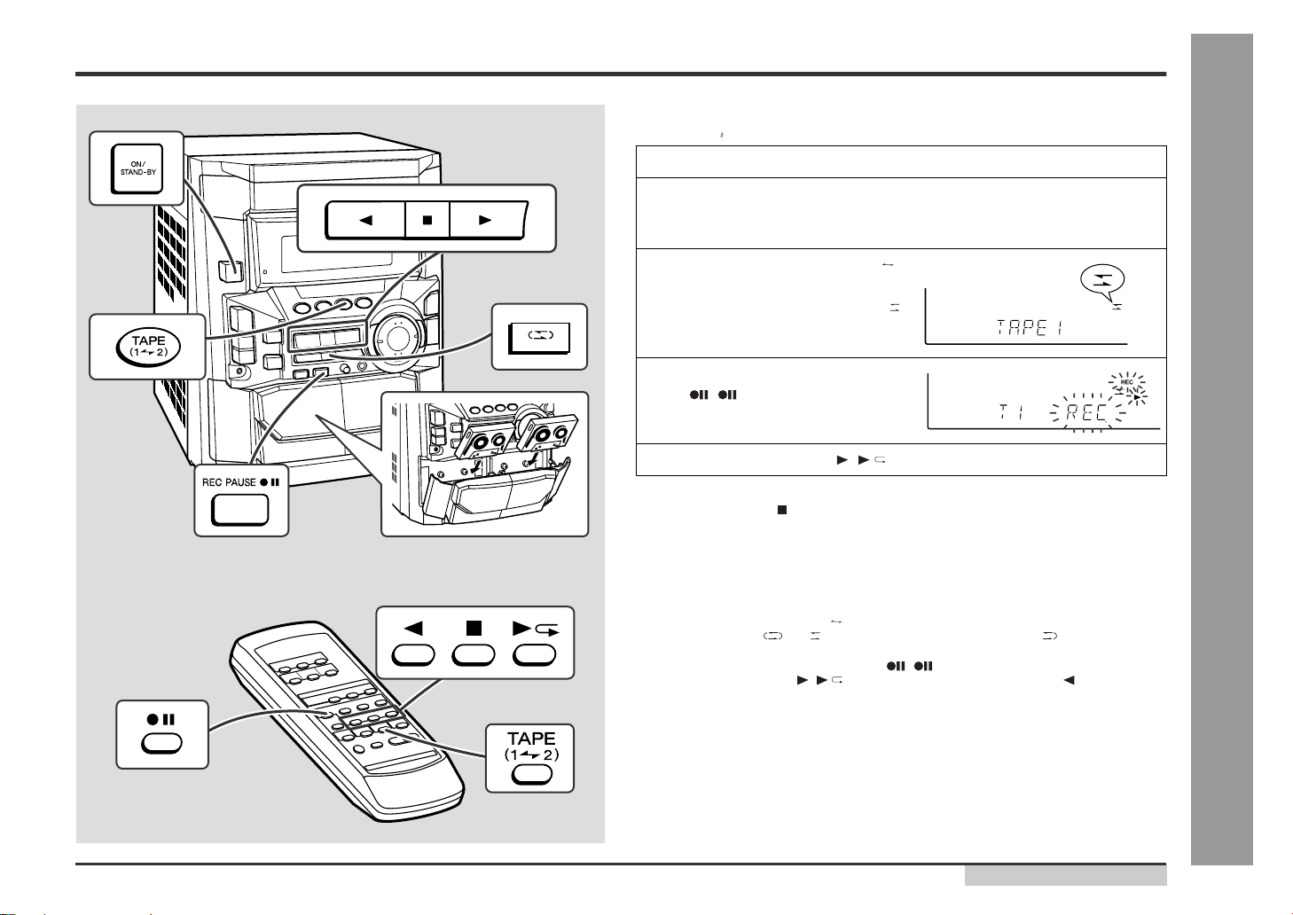
CD-BK250W/CD-BK2600W/CD-BK270W
A
B
C
D
E
F
G
H
1
23456
Figure 8 CD MECHANISM EXPLODED VIEW
– 8 –
CD-BK250W/CD-BK2600W/CD-BK270W
306-1
701
304
701
302
301
702
303
M1
703x2
305x2
SW4
M2
305
PWB-F
306-2
306-3
306
704
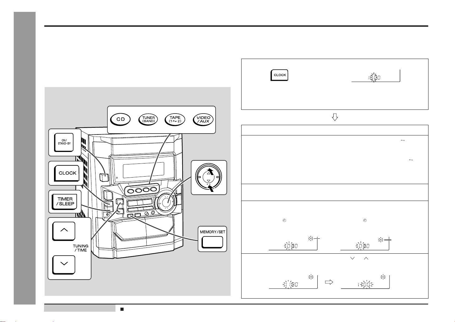
CD-BK250W/CD-BK2600W/CD-BK270W
A
B
C
D
E
F
G
H
1
23456
Figure 9 CABINET EXPLODED VIEW (1/2)
– 9 –
Note: Only the unit and consumable parts are supplied as parts supply for the Tape mechanism.
CD-BK250W/CD-BK2600W/CD-BK270W
202
202-1
202-2
610x2
PWB-A1
603x2
603
223
603
PWB-G2
Tape
Motor
MAIN BELT
FLYWHEEL
ASS'Y
TAPE 1
FLYWHEEL
ASS'Y
TAPE 2
FF/REW
ROLLER
ASS'Y
FF/REW
ROLLER
ASS'Y
BELT CONNECTION
207
610x13
CD-BK270W
ONLY
610x2
610x2
610
610
215
212
262
222
610
610
259
M901
PWB-D
226
223
211
258
258-1~258-11
605x2
611x2
602x3
IC904
IC902
IC903
IC901
608x5
Silicon
Grease
220
PWB-B1
606x12
201-10
201-9
201-14
214
FL701
201
201-11
201-15
201-16
201-25
608
201-24
201-21
201-22
201-13
201-19
201-20
219x2
201-3
201-18
230
613x2
201-7
201-5
201-2
201-17
201-4
201-6
201-12
201-8
PWB-B2
201-16
201-26
201-1
601
608
604
201-21
201-23
201-22
224x8
PWB-A3
PT801
PWB-A2
616x2
616x2
616
610x2
203
203-2
203-1
610
213
218
PWB-G1
601
601
205
604
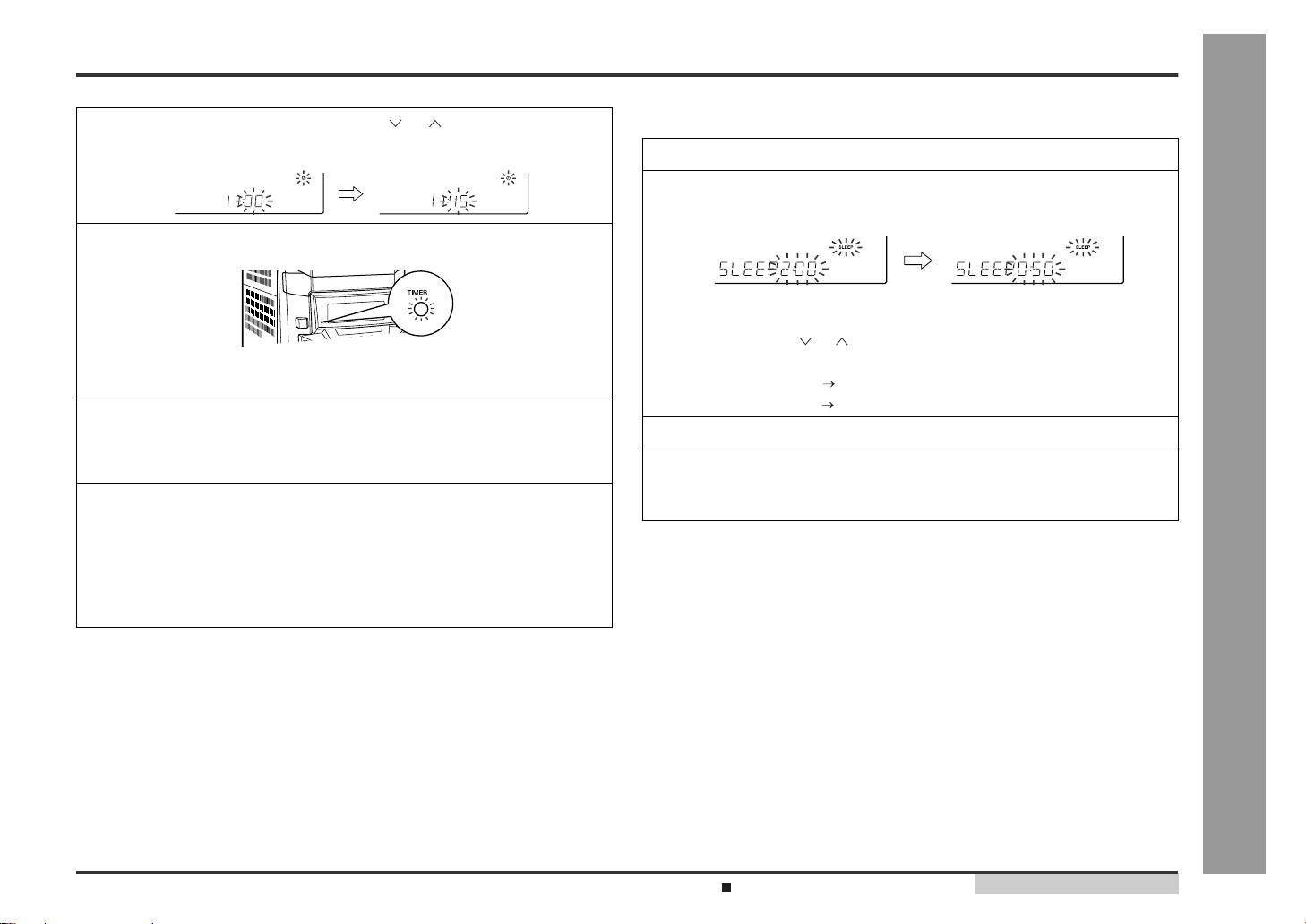
CD-BK250W/CD-BK2600W/CD-BK270W
Figure 10 CABINET EXPLODED VIEW (2/2)
A
B
C
D
E
F
G
H
1
23456
– 10 –
CD
MECHANISM
204
250
228
229
236
254
252
232
232
232x4
PWB-C
232
225
M3
SW3
PWB-E
607x2
607x2
SW2
SW1
247
253
235
251
256
615
206
238
257
241
246
248
245
244
243x4
242
239
249
255
234
231
240
237
614
227
233
260
261
CD-BK250W/CD-BK2600W/CD-BK270W
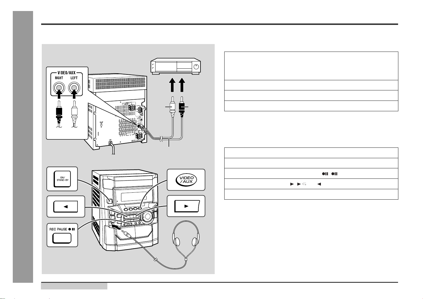
CD-BK250W/CD-BK2600W/CD-BK270W
A
B
C
D
E
F
G
H
1
23456
902
904x4
903
906x2
901
907
908x4
906x2
909x2
905x2
SP3,4
SP1,2
C1,2
Capacitor
2.2µF,100V
(N.P.)
C1,2
Capacitor
2.2µF,100V
Electrolytic (N.P.)
SP3,4
TWEETER
SP1,2
WOOFER
BK
BK
RD
RD
SP1,2
WOOFER
SP3,4
TWEETER
Figure 11 SPEAKER EXPLODED VIEW (1/2)
– 11 –
CP-BK250/CP-BK2600/CP-BK270
CD-BK250W/CD-BK2600W/CD-BK270W
– 12 –
A
B
C
D
E
F
G
H
1
23456
Figure 12 SPEAKER EXPLODED VIEW (2/2)
GBOXS0070AWM1 (CD-BK270W ONLY)
904 x 6
SP1,2
901
902
903
SP1,2
SP1,2
BK
GR
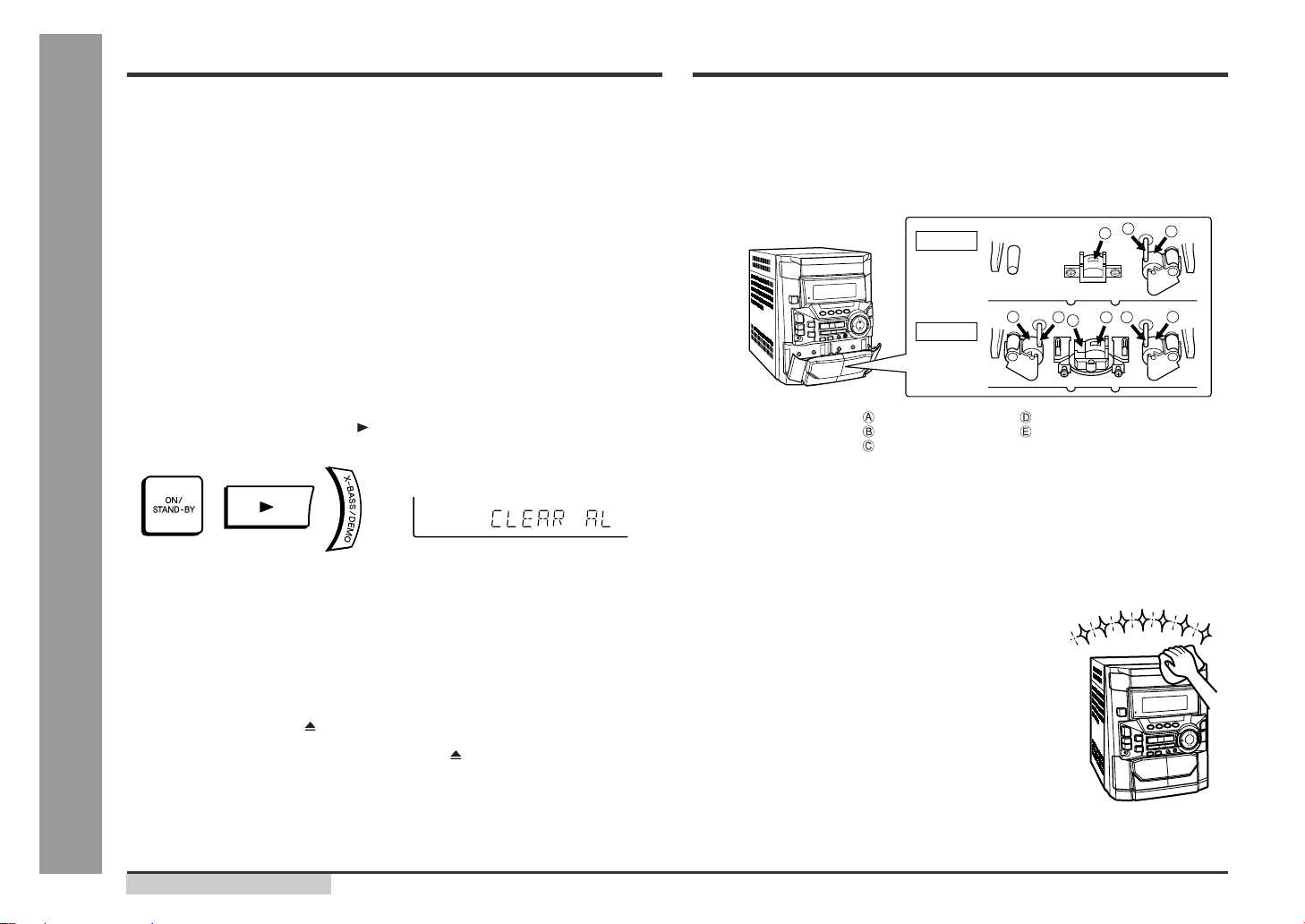
CD-BK250W/CD-BK2600W/CD-BK270W
COPYRIGHT 2001 BY SHARP CORPORATION
ALL RIGHTS RESERVED.
No part of this publication may be reproduced,
stored in a retrieval system, or transmitted in
any form or by any means, electronic, mechanical,
photocopying, recording, or otherwise, without
prior written permission of the publisher.
A0105-1575DS•HA•M
SA • SZ • EX
Printed in Japan
©
SHARP CORPORATION
AV Systems Group
Audio Systems Division
Higashihiroshima, Hiroshima 739-0192, Japan