– 1 –
CD-C451H
SERVICE MANUAL
No. S6840CDC451H/
CONTENTS
Page
SAFETY PRECAUTION FOR SERVICE MANUAL .......................................................................................................... 2
IMPORTANT SERVICE NOTES (U.K. ONLY) ................................................................................................................. 2
SPECIFICATIONS ............................................................................................................................................................ 3
NAMES OF PARTS .......................................................................................................................................................... 4
OPERATION MANUAL ..................................................................................................................................................... 6
DISASSEMBLY................................................................................................................................................................. 7
REMOVING AND REINSTALLING THE MAIN PARTS.................................................................................................. 10
ADJUSTMENT ................................................................................................................................................................ 11
NOTES ON SCHEMATIC DIAGRAM ............................................................................................................................. 18
TYPE OF TRANSISTOR AND LED ................................................................................................................................ 18
BLOCK DIAGRAM .......................................................................................................................................................... 19
SCHEMATIC DIAGRAM / WIRING SIDE OF P.W.BOARD ............................................................................................ 22
WAVEFORMS OF CD CIRCUIT..................................................................................................................................... 44
TROUBLESHOOTING (CD CHANGER CONTROL / CD SECTION)............................................................................. 45
FUNCTION TABLE OF IC .............................................................................................................................................. 49
FL DISPLAY .................................................................................................................................................................... 59
REPLACEMENT PARTS LIST/EXPLODED VIEW
PACKING OF METHOD (FOR U.K. ONLY)
Manufactured under license from Dolby Laboratories Licens-
ing Corporation.
DOLBY, the double-D symbol and "PRO LOGIC"
are trademarks of Dolby Laboratories Licensing Corporation.
SHARP CORPORATION
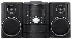
CD-C451H mini component system consisting of
CD-C451H mini component system and
CP-C451H Speaker System.
• In the interests of user-safety the set should be restored to its
original condition and only parts identical to those specified be
used.
CD-C451H
QSOUND and the QLogo are registered trademarks of
QSound Labs, Inc.
QSound is protected under US Patent Nos. 5,105,462
and 5,208,860 and foreign counterparts.
This document has been published to be used
for after sales service only.
The contents are subject to change without notice.
CD-C451H
– 2 –
SAFETY PRECAUTION FOR
SERVICE MANUAL
Precaution to be taken when replacing and servicing the
Laser Pickup.
The AEL (Accessible Emission Level) of Laser Power Output
for this model is specified to be lower than Class I Requirements.
However, the following precautions must be observed during
servicing to protect your eyes against exposure to the Laser
beam
(1) When the cabinet has been removed, the power is turned
on without a compact disc, and the Pickup is on a position
outer than the lead-in position, the Laser will light for several
seconds to detect a disc. Do not look into the Pickup Lens.
(2) The Laser Power Output of the Pickup inside the unit and
replacement service parts have already been adjusted prior
to shipping.
(3) No adjustment to the Laser Power should be attempted
when replacing or servicing the Pickup.
(4) Under no circumstances look directly into the Pickup Lens
at any time.
(5) CAUTION - Use of controls or adjustments, or performance
of procedures other than those specified herein may result
in hazardous radiation exposure.
Laser Diode Properties
Material: GaAIAs
Wavelength: 780 nm
Emission Duration: continuous
Laser Output: max. 0.6 mW
VAROITUS! LAITTEEN KÄYTTÄMINEN MUULLA KUIN TÄSSÄ
KÄYTTÖOHJEESSA MAINITULLA TAVALLA SAATTAA
ALTISTAA KÄYTTÄJÄN TURVALLISUUSLUOKAN 1
YLITTÄVÄLLE NÄKYMÄTTÖMÄLLE LASERSÄTEILYLLE.
VARNING - OM APPARATEN ANVÄNDS PÅANNAT SÄTTÄN I
DENNA BRUKSANVISNING SPECIFICERAS.
KANANVÄNDAREN UTSÄTTAS FÖR OSYNLIG
LASERSTRÅLNING, SOM ÖVERSKRIDER GRÄNSEN FÖR
LASERKLASS 1.
Before returning the unit to the customer after completion of a
repair or adjustment it is necessary for the following withstand
voltage test to be applied to ensure the unit is safe for the
customer to use.
Setting of Withstanding Voltage Tester and set.
Set name set value
Withstanding Voltage Tester
Test voltage 4,240 VPEAK
3,000 VRMS
Set time 6 secs
Set current(Cutoff current) 4 mA
Unit
Judgment
OK: The “GOOD” lamp lights.
NG: The “NG” lamp lights and the buzzor sounds.
SHORT-CIRCUIT
AC POWER
SUPPLY CORD
CONNECT THE PROBE
TO GND TERMINAL
OF PHONO TERMINAL
PROBE
AC
UNIT
WITHSTANDING
VOLTAGE TESTER
+
-
OUT
IMPORTANT SERVICE NOTES (FOR U.K. ONLY)
(FOR U.K./Australia/New zealand)
LASER KLASSE 1
LUOKAN 1 LASERLAITE
KLASS 1 LASERAPPARAT
(Except For U.K./Australia/New zealand)
CAUTION-INVISIBLE LASER RADIATION WHEN OPEN. DO NOT STARE INTO
BEAM OR VIEW DIRECTLY WITH OPTICAL INSTRUMENTS.
VARNING-OSYNLIG LASERSTRALNING NAR DENNA DEL AR OPPNAD. STIRRA
EJ IN I STRALEN OCH BETRAKTA EJ STRALEN MED OPTISKA INSTRUMENT.
ADVERSEL-USYNLIG LASERSTRALING VED ABNING. SE IKKE IND I
STRALEN-HELLER IKKE MED OPTISKE INSTRUMENTER.
VARO! AVATTAESSA OLET ALTTIINA NAKYMATON LASERSATEILYLLE.
ALA TUIJOTA SATEESEEN ALAKA KATSO SITA OPTISEN LAITTEEN LAPI.
VARNING-OSYNLIG LASERSTRALNING NAR DENNA DEL AR OPPNAD.
STIRRA EJ IN I STRALEN OCH BETRAKTA EJ STRALEN GENOM OPTISKT
INSTRUMENT.
ADVERSEL-USYNLIG LASERSTRALING NAR DEKSEL APNES. STIRR IKKE
INN I STRALEN ELLER SE DIREKTE MED OPTISKE INSTRUMENTER.
CHASSIS
SCREW
CONNECT THE PROBE
TO GND TERMINAL OF
CHASSIS SCREW
– 3 –
CD-C451H
SPECIFICATIONS
FOR A COMPLETE DESCRIPTION OF THE OPERATION OF THIS UNIT, PLEASE REFER
TO THE OPERATION MANUAL.
Specifications for this model are subject to change without
prior notice.
CD-C451H
General
Power source: AC 230-240 V, 50 Hz
Power
consumption: 81 W
Dimensions: Width; 270 mm (10-5/8")
Height; 303 mm (11-13/16")
Depth; 350 mm (13-13/16")
Weight: 6.6 kg (14.2 lbs.)
Amplifier section
Output power:
(
Except FOR GERMANY
)
(
Except FOR GERMANY
)
Output power:
(FOR GERMANY)
MPO; 176 W (88 W + 88 W)
(10 % T.H.D.)
RMS; 80 W (40 W + 40 W)
(10 % T.H.D.)
Input terminals: Video/Auxiliary (audio sig-
nal) ¥ 2; 500 mV/47 kohms
Output terminals: Speakers; 6 ohms
Headphones; 16-50 ohms
(recommended; 32 ohms)
Pre-output; 500 mV/47
kohms
Compact disc player section
Type: 3-disc multi-play compact
disc player
Signal readout: Non-contact, 3-beam semi-
conductor laser pickup
D/A converter: 1-bit D/A converter
Frequency
response: 20 - 20,000 Hz
Dynamic range: 90 dB (1 kHz)
Tuner section
Frequency range: FM; 87.5 - 108 MHz
MW; 522 - 1,620 kHz
LW; 153 - 281 kHz
Cassette deck section
Type: Compact cassette tape
Frequency response: 50 - 14,000 Hz (Normal tape)
Motor: DC motor with electronic governor ¥ 1
Signal/noise ratio: 55 dB (TAPE 1, playback)
50 dB (TAPE 2, recording/playback)
Bias and erasure
system:
AC
Tape speed: 4.76 cm/sec. (1-7/8 ips.)
Wow and flutter: 0.15 % (WRMS)
(FOR GERMANY)
Wow and flutter:
Heads: TAPE-1: Playback 1
TAPE-2: Record/playback ¥ 1
Erase ¥ 1
Speaker section
Type: 3-way type [130 mm (5-1/8") woofer,
50 mm (2") tweeter and super tweeter]
Maximum input power: 80 W
Impedance: 6 ohms
Dimensions: Width; 200 mm (7-7/8")
Height; 300 mm (11-13/16")
Depth; 253 mm (10")
Weight: 2.7 kg (5.8 lbs.)/each
PMPO; 352 W (total)
MPO; 176 W (88 W + 88 W)
(DIN 45 324)
RMS; 80 W (40 W + 40 W)
(DIN 45 324)
0.2 % (DIN 45 511, playback)
CP-C451H
CD-C451H
– 4 –
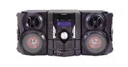
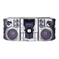
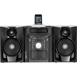
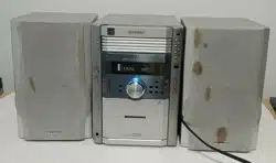
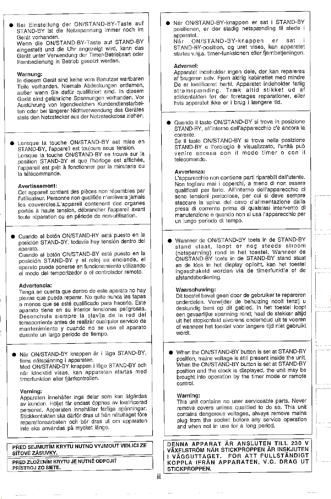
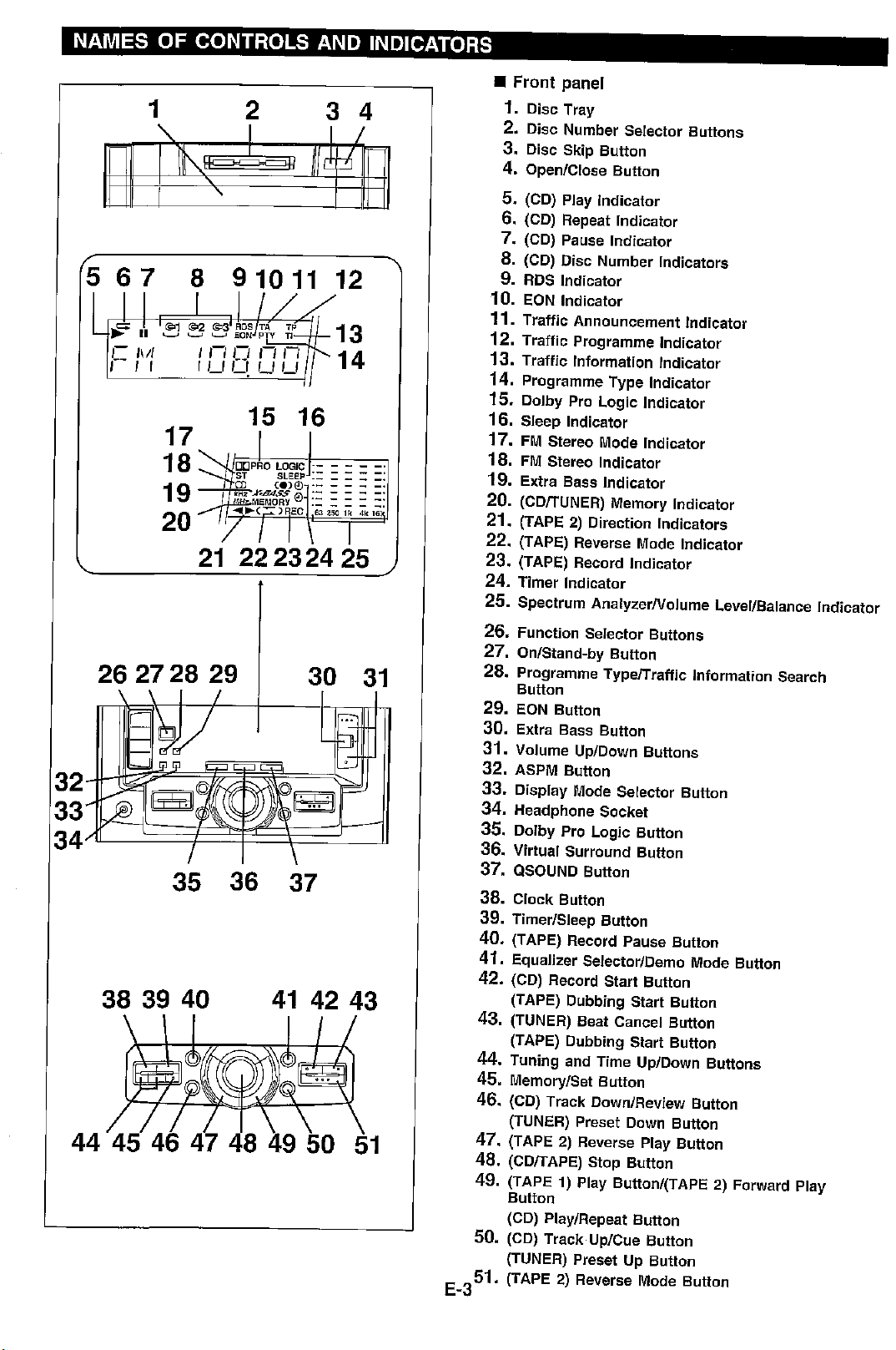
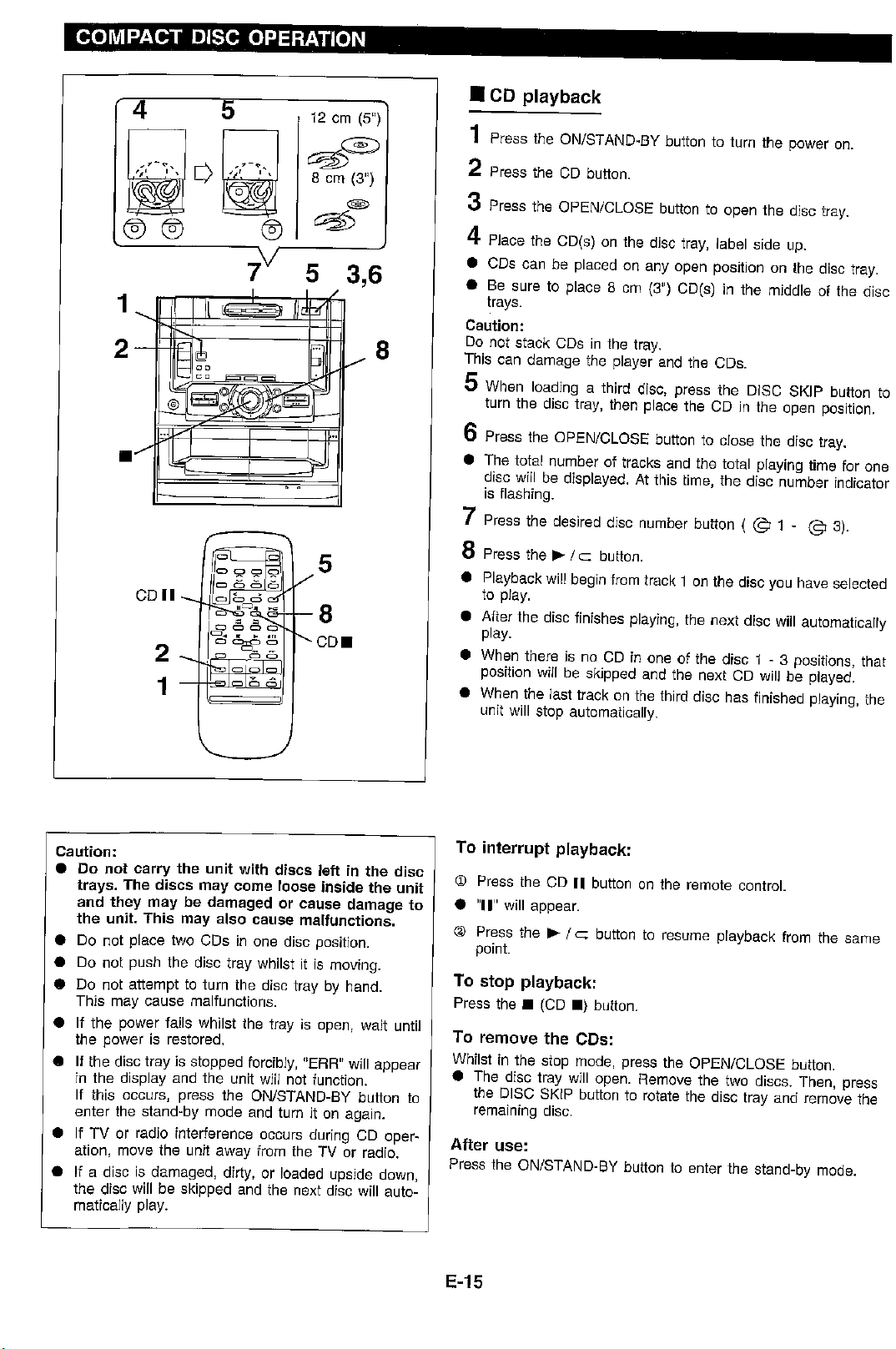
NAMES OF PARTS
CD-C451H
Front panel
11. Disc Tray
12. Disc Number Selector Buttons
13. Disc Skip Button
14. Open/Close Button
15. (CD) Play Indicator
16. (CD) Repeat Indicator
17. (CD) Pause Indicator
18. (CD) Disc Number Indicators
19. RDS Indicator
10. EON Indicator
11. Traffic Announcement Indicator
12. Traffic Programme Indicator
13. Traffic Information Indicator
14. Programme Type Indicator
15. Dolby Pro Logic Indicator
16. Sleep Indicator
17. FM Stereo Mode Indicator
18. FM Stereo Indicator
19. Extra Bass Indicator
20. (CD/TUNER) Memory Indicator
21. (TAPE 2) Direction Indicators
22. (TAPE) Reverse Mode Indicator
23. (TAPE) Record Indicator
24. Timer Indicator
25. Spectrum Analyzer/Volume Level/Balance Indicator
26. Function Selector Buttons
27. On/Stand-by Button
28. Programme Type/Traffic Information Search Button
29. EON Button
30. Extra Bass Button
31. Volume Up/Down Buttons
32. ASPM Button
33. Display Mode Selector Button
34. Headphone Socket
35. Dolby Pro Logic Button
36. Virtual Surround Button
37. QSOUND Button
38. Clock Button
39. Timer/Sleep Button
40. (TAPE) Record Pause Button
41. Equalizer Selector/Demo Mode Button
42. (CD) Record Start Button
3 (TAPE) Dubbing Start Button
43. (TUNER) Beat Cancel Button
3 (TAPE) Dubbing Start Button
44. Tuning and Time Up/Down Buttons
45. Memory/Set Button
46. (CD) Track Down/Review Button
3 (TUNER) Preset Down Button
47. (TAPE 2) Reverse Play Button
48. (CD/TAPE) Stop Button
49. (TAPE 1) Play Button/(TAPE 2) Forward Play Button
3 (CD) Play/Repeat Button
50. (CD) Track Up/Cue Button
3 (TUNER) Preset Up Button
51. (TAPE 2) Reverse Mode Button
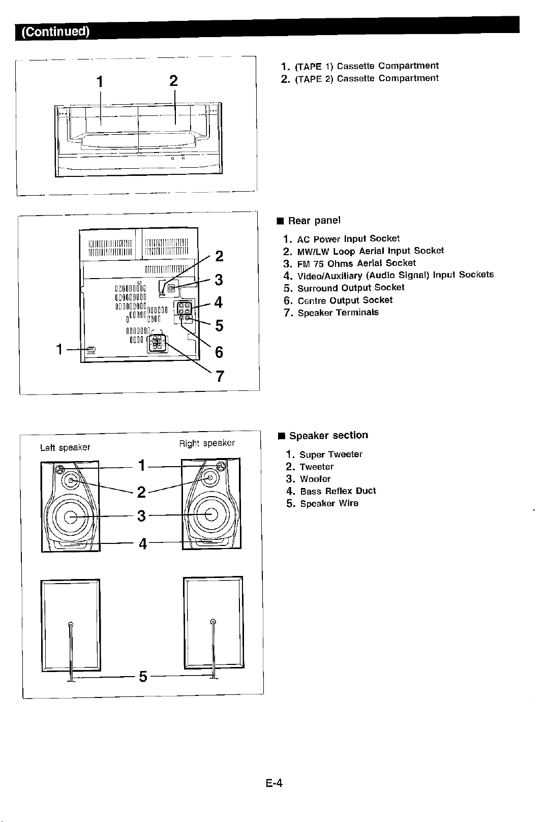
52. (TAPE 1) Cassette Compartment
53. (TAPE 2) Cassette Compartment
1
234
123
X-BASS
kHz
MHz
RDS
EON
TA
PTY
TP
63 250 1k 4k 16k
SLEEPST
MEMORY
PRO LOGIC
REC
TI
5
6
7
8
9
13
14
10 11
12
17
18
19
15 16
20
21
22
2324 25
26
27 28 29
30
31
32
33
34
35
36
37
38 39 40
41 42 43
44 45 46 47 48 49 50
51
52
53
– 5 –
CD-C451H
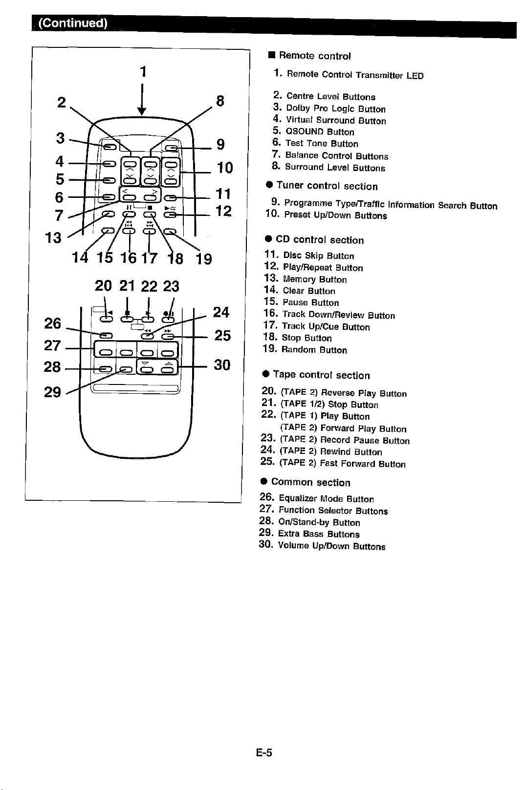
Remote control
11. Remote Control Transmitter LED
12. Centre Level Buttons
13. Dolby Pro Logic Button
14. Virtual Surround Button
15. QSOUND Button
16. Test Tone Button
17. Balance Control Buttons
18. Surround Level Buttons
Tuner control section
19. Programme Type/Traffic Information Search Button
10. Preset Up/Down Buttons
CD control section
11. Disc Skip Button
12. Play/Repeat Button
13. Memory Button
14. Clear Button
15. Pause Button
16. Track Down/Review Button
17. Track Up/Cue Button
18. Stop Button
19. Random Button
Tape control section
20. (TAPE 2) Reverse Play Button
21. (TAPE 1/2) Stop Button
22. (TAPE 1) Play Button
3 (TAPE 2) Forward Play Button
23. (TAPE 2) Record Pause Button
24. (TAPE 2) Rewind Button
25. (TAPE 2) Fast Forward Button
Common section
26. Equalizer Mode Button
27. Function Selector Buttons
28. On/Stand-by Button
29. Extra Bass Buttons
30. Volume Up/Down Buttons
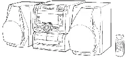
CD-C451H
CD-C451H
CP-C451H
1
2
3
4
5
Left speaker
Right speaker
1
2
3
4
5
6
7
Rear panel
11. AC Power Input Socket
12. MW/LW Loop Aerial Input Socket
13. FM 75 Ohms Aerial Socket
14. Video/Auxiliary (Audio Signal) Input Sockets
15. Surround Output Socket
16. Centre Output Socket
17. Speaker Terminals
Speaker section
11. Super Tweeter
12. Tweeter
13. Woofer
14. Bass Reflex Duct
15. Speaker Wire
1
2
3
4
5
6
9
7
10
11
13
14 15 16 17 18 19
20
21
22
23
26
27
28
29
24
25
30
12
8
CD-C451H
– 6 –
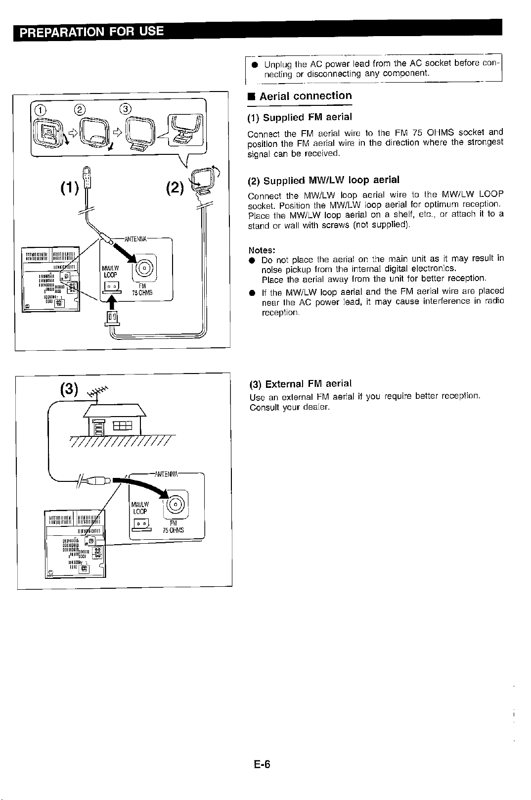
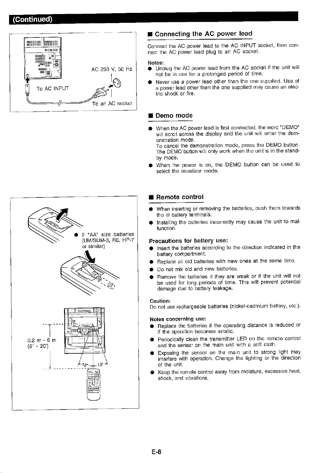
RESETTING THE MICROCOMPUTER
Reset the microcomputer under the following conditions:
To erase all of the stored memory contents (clock and timer
settings, and tuner and CD presets).
If the display is not correct.
If the operation is not correct.
1
Press the ON/STAND-BY button to enter the stand-by mode.
2
While pressing down the VOLUME button and the TUN-
ING/TIME button, hold down the ON/STAND-BY button for
at least 1 second.
Caution:
The operation explained above will erase all data stored in
memory including clock and timer settings, and tuner and CD
presets.
1,2
2
2
OPERATION MANUAL
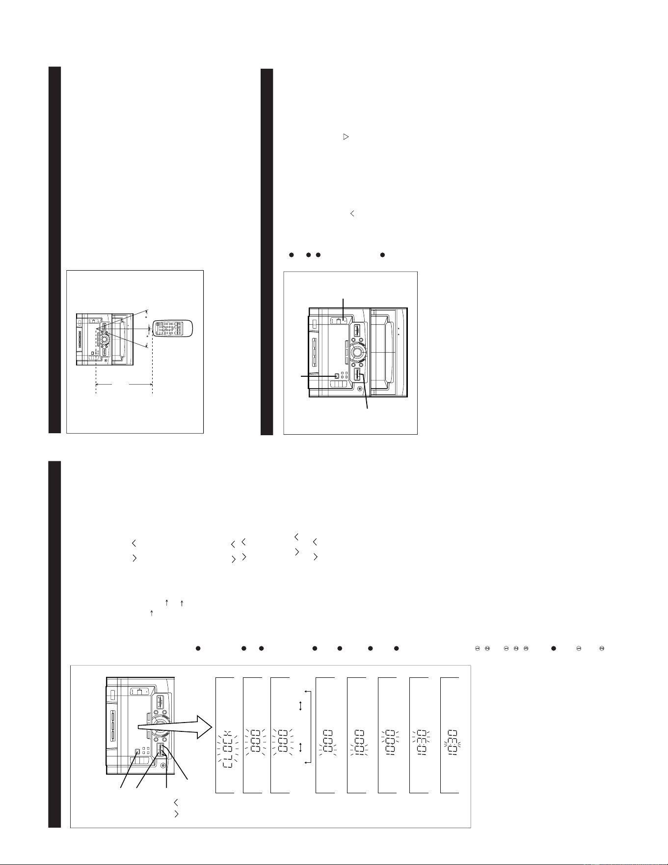
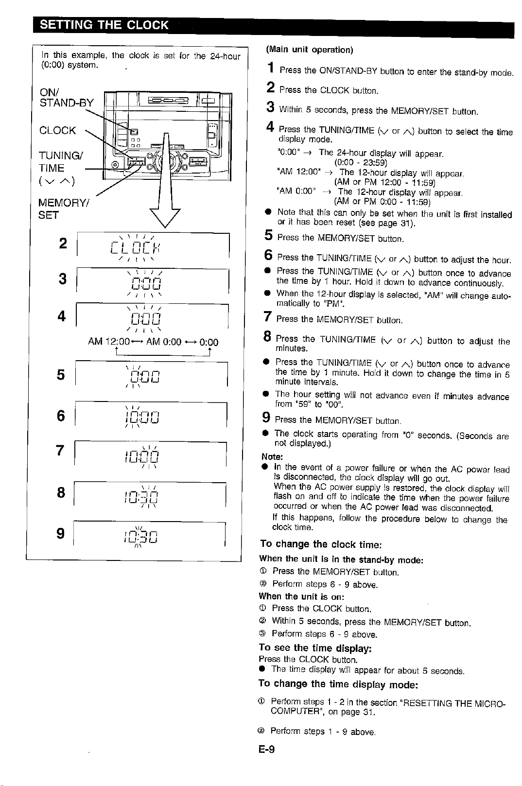
SETTING THE CLOCK
(Main unit operation)
1
Press the ON/STAND-BY button to enter the stand-by mode.
2
Press the CLOCK button.
3
Within 5 seconds, press the MEMORY/SET button.
4
Press the TUNING/TIME ( or ) button to select the time
display mode.
"0:00"
The 24-hour display will appear.
(0:00 - 23:59)
"AM 12:00"
The 12-hour display will appear.
(AM or PM 12:00 - 11:59)
"AM 0:00"
The 12-hour display will appear.
(AM or PM 0:00 - 11:59)
Note that this can only be set when the unit is first installed
or it has been reset.
5
Press the MEMORY/SET button.
6
Press the TUNING/TIME ( or ) button to adjust the hour.
Press the TUNING/TIME ( or ) button once to advance
the time by 1 hour. Hold it down to advance continuously.
When the 12-hour display is selected, "AM" will change auto-
matically to "PM".
7
Press the MEMORY/SET button.
8
Press the TUNING/TIME ( or ) button to adjust the
minutes.
Press the TUNING/TIME ( or ) button once to advance
the time by 1 minute. Hold it down to change the time in 5
minute intervals.
The hour setting will not advance even if minutes advance
from "59" to "00".
9
Press the MEMORY/SET button.
The clock starts operating from "0" seconds. (Seconds are
not displayed.)
Note:
In the event of a power failure or when the AC power lead
is disconnected, the clock display will go out.
When the AC power supply is restored, the clock display will
flash on and off to indicate the time when the power failure
occurred or when the AC power lead was disconnected.
If this happens, follow the procedure below to change the
clock time.
To change the clock time:
When the unit is in the stand-by mode:
Press the MEMORY/SET button.
Perform steps 6 - 9 above.
When the unit is on:
Press the CLOCK button.
Within 5 seconds, press the MEMORY/SET button.
Perform steps 6 - 9 above.
To see the time display:
Press the CLOCK button.
The time display will appear for about 5 seconds.
To change the time display mode:
Perform steps 1 - 2 in the section "RESETTING THE MICRO-
COMPUTER",.
Perform steps 1 - 9 above.
In this example, the clock is set for the 24-hour
(0:00) system.
ON/
STAND-BY
CLOCK
MEMORY/
SET
TUNING/
TIME
( )
0:00 AM 0:00AM 12:00
2
3
4
5
6
7
8
9
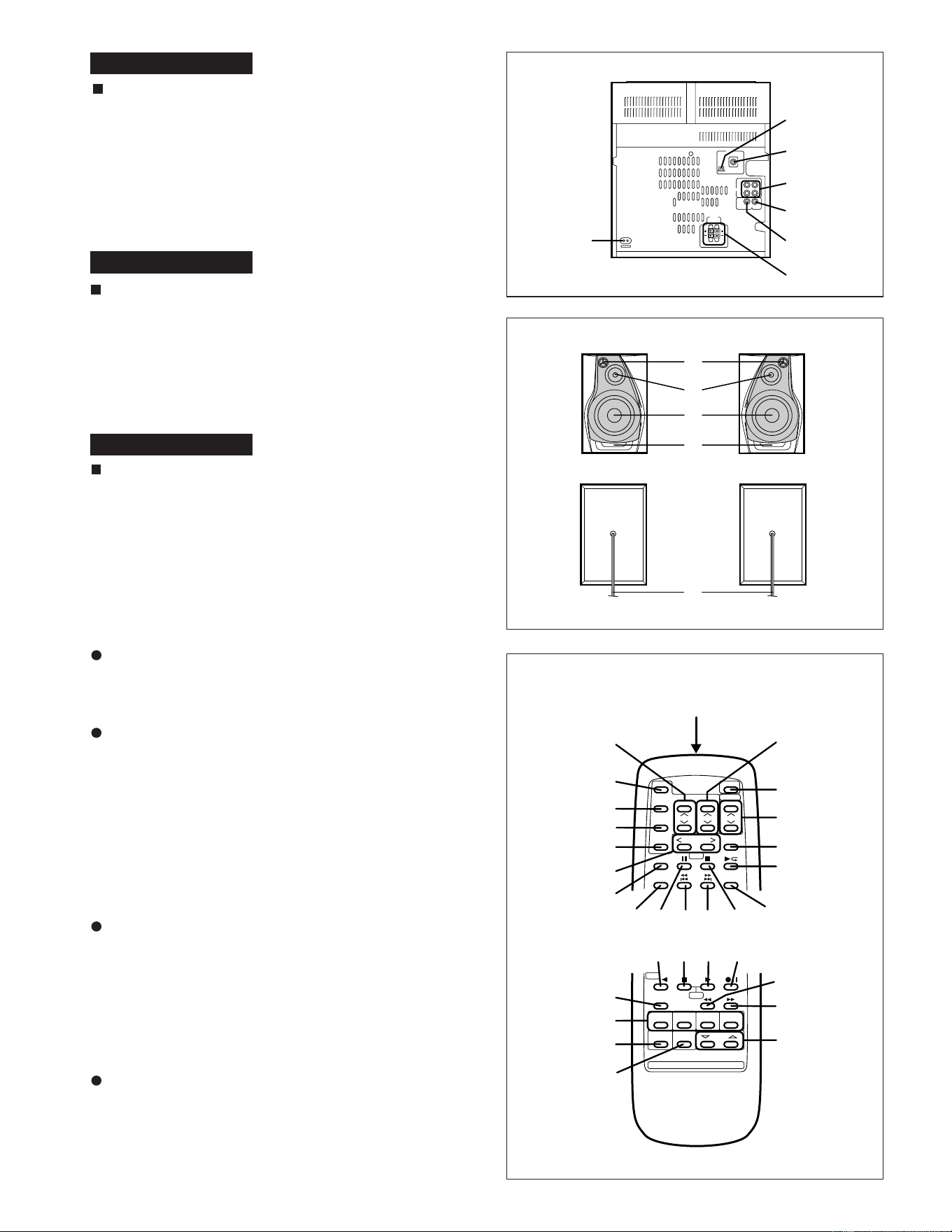
PREPARTION FOR USE
15
15
Notes concerning use:
● Replace the batteries if the operating distance becomes re-
duced or if operation becomes erratic.
● Periodically clean the transmitter LED on the remote control
and the sensor on the main unit with a soft cloth.
● Exposing the sensor on the main unit to strong light may
interfere with operation. Change the lighting or the direction
of the unit.
● Keep the remote control away from moisture, excessive heat,
shock, and vibrations.
0.2 m - 6 m
(8" - 20')
– 7 –
CD-C451H
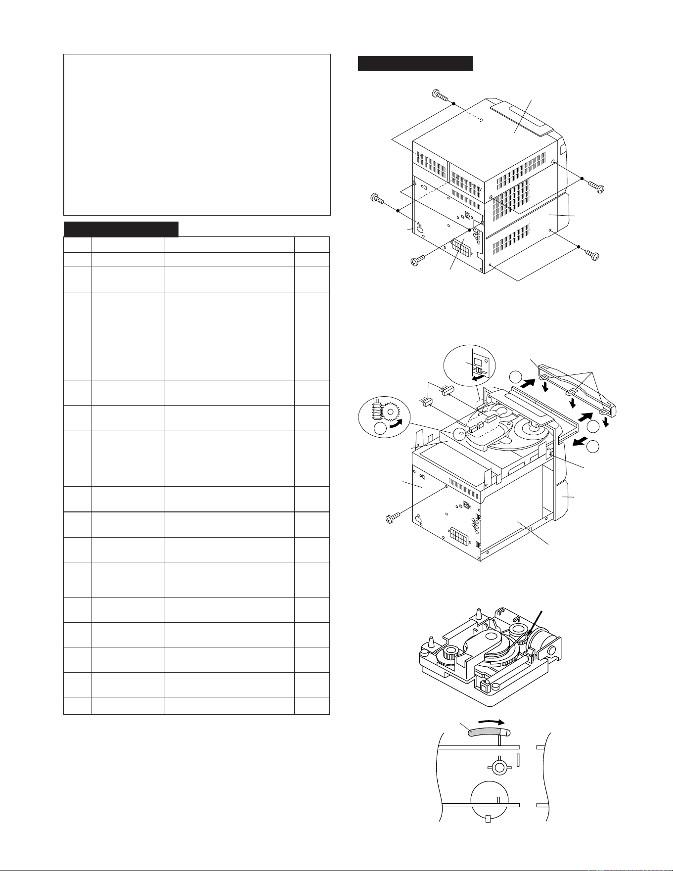
DISASSEMBLY
Caution on Disassembly
Follow the below-mentioned notes when disassembling
the unit and reassembling it, to keep it safe and ensure
excellent performance:
1. Take cassette tape and compact disc out of the unit.
2. Be sure to remove the power supply plug from the wall
outlet before starting to disassemble the unit.
3. Take off nylon bands or wire holders where they need to
be removed when disassembling the unit. After servicing
the unit, be sure to rearrange the leads where they were
before disassembling.
4. Take suffcient care on static electricity of integrated
circuits and other circuits when servicing.
Figure 7-2
Figure 7-3
1 Top Cabinet 1. Screw ..................... (A1) x4 7-1
2 Side Panel 1. Screw ..................... (B1) x6 7-1
(Left/right)
3 CD Player Unit/ 1. Turn on the power supply, 7-2
CD Tray Cover open the disc tray, take out
the CD cover, and close.
(Note 1)
2. Hook ...................... (C1) x3
3. Hook ...................... (C2) x2
4. Screw .................... (C3) x1
5. Socket ................... (C4) x2
4 Back Board 1. Screw .................... (D1) x12 8-1
2. Socket ................... (D2) x1
5 Tuner PWB 1. Screw .................... (E1) x1 8-1
2. Socet ..................... (E2) x1
6 Main PWB 1. Screw .................... (F1) x1 8-2
2. Socket ................... (F2) x2
3. Flat Wire................ (F3) x2
4. Tip Wire ................. (F4) x1
5. Socket ................... (F5) x1
7
Front Panel
1. Screw .................... (G1) x2 8-2
2. Hook ...................... (G2) x2
8 Display PWB/ 1. Screw .................... (H1) x12 8-3
Switch PWB
9 Tape Mechanism 1. Open the cassette holder. 8-3
2. Screw .................... (J1) x5
10
Power Amp. PWB
1. Screw .................... (K1) x4 8-4
2. Socket ................... (K2) x2
3. Push Rivet ............ (K3) x4
11
CD Servo PWB
1. Screw .................... (L1) x1 8-5
2. Cover .................... (L2) x4
12 Turntable 1. Screw .................... (M1) x1 8-6
2. Cover .................... (M2) x1
13 CD Player Base 1. Screw .................... (N1) x2 8-6
2. Guide .................... (N2) x2
14 CD Changer 1. Screw .................... (P1) x4 8-7
Mechanism
15 CD Mechanism 1. Screw .................... (Q1) x1 8-7
STEP REMOVAL PROCEDURE FIGURE
Note 1:
How to open the changer manually. (Fig.7-3)
1. Insert the tip of fine screwdriver into the hole of CD player
base, and press down the worm wheel < A > .
2. Then, turn fully the lock lever in the arrow direction through
the hole on the loading chassis bottom in this state.
After that, push forward the CD player base.
Figure 7-1
CD-C451H
CD-C451H
( B1 ) x2
ø3 x8mm
( B1 ) x2
ø3 x8mm
( B1 ) x2
ø3 x8mm
Top Cabinet
Side Panel
(Right)
Back Board
Side Panel
(Left)
( A1 ) x2
ø3 x12mm
( A1 ) x2
ø3 x12mm
CD Tray Cover
CD Player Unit
( C3 ) x1
ø3 x8mm
Hook
( C1) x3
( C2 ) x1
( C4 ) x2
Back Board
Main PWB
Front Panel
1
1
2
A
Pull
(C2) x1
LOCK
LEVER
< A >
CD-C451H
– 8 –
( D1 ) x2
ø3 x10mm
( E1 ) x1
ø3 x10mm
( D1 ) x1
ø3 x10mm
Main PWB
Tuner
PWB
Front Panel
( D1 ) x9
ø3 x8mm
( D2 ) x1
( E2 ) x1
Back Board
( F2 ) x2
( F3 ) x1
(F5) x1
( F4 ) x1
( F1 ) x1
ø3 x10mm
( G1 ) x2
ø3 x8mm
( G2 ) x1
( G2 ) x1
Main PWB
( F3 ) x1
Push
Push
Front Panel
Tape
Mechanism
Power Amp.
PWB
Display
PWB
Switch PWB
Open
Front Panel
( H1 ) x3
ø3 x10mm
( H1 ) x9
ø3 x10mm
( J1 ) x5
ø3 x10mm
Tape
Mechanism
Cassette
Holder
(Left/Right)
( K1 ) x4
ø3 x12mm
( K2 ) x1
( K2 ) x1
( K3 ) x4
Power Amp.
PWB
Power
Transformer
( L1 ) x1
ø3 x10mm
( L2 ) x2
( L2 ) x2
Loading chassis
CD Servo PWB
( N1 ) x1
ø3 x10mm
( N1 ) x1
ø3 x10mm
( M1 ) x1
ø3 x10mm
Washer
Turntable
CD Player Base
( M2 ) x1
( N2 ) x1
( N2 ) x1
Loading chassis
( P1 ) x4
ø3 x12mm
( Q1 ) x1
ø2.6 x10mm
CD Changer
Mechanism
CD Mechanism
Shift Lever
CD Player Base
Figure 8-1
Figure 8-2
Figure 8-3
Figure 8-4
Figure 8-5
Figure 8-6
Figure 8-7
Be careful when installing the CD changer mechanism.
Install the CD changer mechanism on the CD player base after
the shift lever has been set in the highest position.
– 9 –
CD-C451H
CP-C451H
1 Front Speaker 1. Net.......................... (A1) x1 9-1
2. Fromt Panel ........... (A2) x1
3. Screw ..................... (A3) x2 9-2
4. Screw ..................... (A4) x4
5. Screw ..................... (A5) x2
STEP REMOVAL PROCEDURE FIGURE
CP-C451H
Figure 9-2
Figure 9-1
Screwdriver
Net
( A1 ) x1
Front Panel
( A2 ) x1
Woofer
Tweeter
( A3 ) x2
ø3 x10mm
( A5 ) x2
ø3 x10mm
( A4 ) x4
ø4 x14mm
Woofer
Tweeter
Super
Tweeter
CD-C451H
– 10 –
Figure 10-2
How to remove the pickup (See Fig. 10-2)
1. Remove the screws (B1) x 2 pcs., to remove the shaft (B2)
x 1 pc.
2. Remove the stop washer (B3) x 1 pc., to remove the gear
(B4)x 1 pc.
3. Remove the pickup.
REMOVING AND REINSTALLING THE MAIN PARTS
CD MECHANISM SECTION
Perform steps 1, 2, 3, 14 and 15 of the disassembly method
to remove the CD mechanism.
How to remove the turntable up/down motor
(See Fig. 10-1)
1. Remove the screws (A1) x 2 pcs., to remove the turntable
up/down motor.
Figure 10-1
( B1 ) x2
2.6 x6mm
Shaft
( B2 ) x1
Stop Washer
( B3 ) x1
Gear
( B4 ) x1
CD Mechanism
Pickup
( A1 ) x2
ø2 x5mm
Turntable Up/Down Motor
Ø
Ø
– 11 –
CD-C451H
MECHANISM SECTION
• Driving Force Check
Torque Meter Specified Value
Play: TW-2412 Tape 1: Over 80 g
Tape 2: Over 80 g
• Torque Check
Torque Meter
Tape 2
Play: TW-2111 30 to 60 g. cm 30 to 100 g.cm
Fast forward: TW-2231 — 50 to 100 g.cm
Rewind: TW-2231 — 50 to 100 g.cm
Specified
Value
Adjusting
Point
Instrument
Connection
Test Tape
Normal MTT-111 VRM1 3,000 ± Speaker
speed 30 Hz terminal
ADJUSTMENT
Specified Value
Tape 1
• Tape Speed
fL: Low-range frequency
fH: High-renge frequency
• AM IF/RF
Signal generator: 400 Hz, 30%, AM modulated
IF 450 kHz 1,620 kHz T351 *1
MW Band — 522 kHz (fL): T306 *2
Coverage 1.1 ± 0.1 V
MW 990 kHz 990 kHz (fL): T302 *1
Tracking
LW Band — 153 kHz (fL): T305 *2
Coverage 1.5 ± 0.1 V
LW 225 kHz 225 kHz (fL): T301 *1
Tracking
Test Stage
Frequency Frequency
Display
Setting/
Adjusting
Parts
Instrument
Connection
• FM
Notes:
1: Description of the "FM IF Adjustment" is not carried on this
Manual. It is because the IF coil in the FM front end section
has been best adjusted in the factory so that its further
adjustment is not needed at the field. When replacing the
FM front end assembly, no adjustment is needed either.
2: The parts in the FM front end section are prepared in a
complete unit, so you can't obtain each part individually
Adjusting
Parts
Instrument
Connection
Frequency
Display
Frequency
• FM Mute Level
Signal generator: 1 kHz, 40 kHz dev., FM modulated
98.00 MHz 98.00 MHz VR351 Input: Antenna
(25 dBµV) Output: Speaker
Terminal
Figure 11 ADJUSTMENT POINTS
TUNER SECTION
*1. Input: Antenna, Output: TP302
*2. Input: Antenna, Output: TP301
VRM1
TAPE
SPEED
TAPE MECHANISM PWB
TUNER PWB
TP301
CNP301
SO301
ANTENNA
TERMINAL
FE301
TP302
R357
T351
T306
T305 T302 T301
VR351
AM IF
FM MUTE
LEVEL
MW BAND
COVERAGE
MW
TRACKING
LW
TRACKING
LW BAND
COVERAGE
CD-C451H
– 12 –
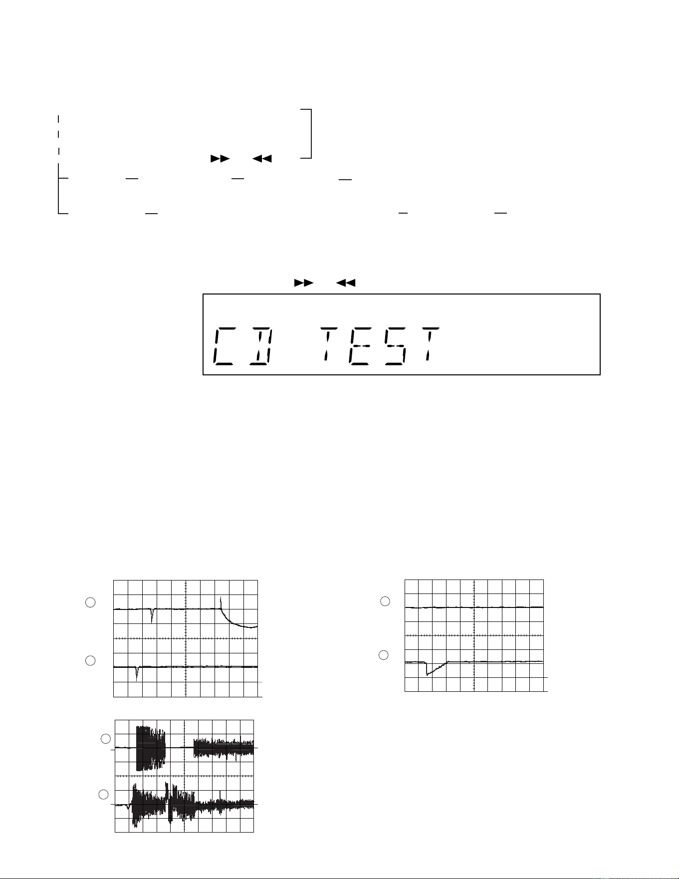
TEST MODE
Figure 12-2
Figure 12-3
Since this CD system incorporates the following automatic adjustment function, when the pickup is replaced, it is not necessary
to readjust it.
Since this CD unit does not need adjustment, the combination of PWB and laser pickup unit is not restricted.
• Automatic adjustment item
1. Focus offset (Fig.12-2)
2. Tracking offset (Fig.12-3)
3. E/F balance (tracking error balance) (Fig.12-4)
4. RF level AGC function (HF level: constant)
5. RF level automatic follow-up of the tracking gain
This automatic adjustment is performed each time a disc is changed. Therefore,
each disc is played back using the optimal settings.
CD SECTION
Figure 12-1
Note:
Only in STOP state it is possible to slide the pickup with the ( ) or ( ) key.
VOL. --- Last memory
BAL. --- CENTER
R.GEQ. --- FLAT
X-BAS --- OFF
Canceling method - POWER OFF
• Setting the test mode
Any one of test mode can be set by pressing several keys as follows.
<REC. PAUSE> + <CD> + <POWER> TEST: CD operation test
• TEST mode
Function — CD test mode
Setting of TEST mode
Indication of CD TST mode (Fig.12-1)
OPEN/CLOSE operation is manual operation.
The pickup can be moved by using the (
) or ( ) key.
<MEMORY>
LASER ON
<PLAY> key input Press <STOP> key.
Stop
TOC. IL is performed, and the ordinary PLAY is performed.
If the following key is pressed during PLAY, it is possible
to specify directly any Track No.
<Disc Number 1> key: Track 4
<Disc Number 2> key: Track 9
<Disc Number 3> key: Track 15
<MEMORY>
Tracking on the spot.
SERVO OFF PLAY
<MEMORY>
Tracking on the spot.
SERVO ON PLAY
STOP
Figure 12-4
IL is not performed.
<STOP>
2
1
10ms
0.50 V
IC1 20 FE
10ms
0.50 V
IC1 7 TE
Enlarged
View
TRACKING
OFF-SET
ADJUST
2
1
TO
TE
200 ms
1V/diV
IC 1 15
200 ms
1V/diV
IC 1 7
TRACKING/
ERROR
BARANCE
ADJUST
2
0.1s
0.50 V
IC1 20 FE
0.1s
0.50 V
IC1 7 TE
1
FOCUS
OFF-SET
ADJUST
TRACKING
OFF-SET
ADJUST
– 13 –
CD-C451H
SP out L-ch Input signal is output.
(SO901) R-ch Input signal is output.
(SO901) SP out C-ch SP cut, no output
(SO901) SP out S-ch
Almost no output (only omitting component)
SP out L-ch Almost no output (only omitting component)
(SO901) R-ch Almost no output (only omitting component)
(SO901) SP out C-ch
Input signal is output.
(SO901) SP out S-ch
Almost no output (only omitting component)
State of set Dolby Pro Logic Dolby Pro Logic On mode
Output point Bypass mode Normal mode Phantom mode
IC501 12 pin L-out Output enabled state Output enabled state Output enabled state
11 pin R-out Output enabled state Output enabled state Output enabled state
IC501 9 pin C-out No output Output enabled state No output
IC501 10 pin S-out No output Output enabled state Output enabled state
SP OUT L-ch Output enabled state Output enabled state Output enabled state
(SO901) R-ch Output enabled state Output enabled state Output enabled state
SP OUT C-ch No output in MUTE (Q604) state Output enabled state No output in MUTE (Q604) state
(SO901)
SP OUT S-ch No output in MUTE (Q603) state Output enabled state Output enabled state
(SO901)
EXPLANATION OF DOLBY SURROUND PRO LOGIC AND EVALUATION METHOD
Test tone output
• Pro Logic ON Normal mode
Press the remote control TEST TONE button.
→Output of only L-ch →Output of only C-ch
↑ ↓
Output of only S-ch ← Output of only R-ch
The test tone (noise) is repeatedly output for output period
(2 sec).
In this case the following indication appears repeatedly.
→TEST →L-ch →C-ch
↑ ↓
S-ch ← R-ch
• Pro Logic ON Phantom mode
Press the remote control TEST TONE button.
→Output of only L-ch →Output of only R-ch
↑ ↓
← Output of only S-ch
The test tone (noise) is repeatedly output for output period
(2 sec).
In this case the following indication appears repeatedly.
→TEST → L-ch → R-ch
↑ ↓
← S-ch←
Outline
• Namely, two speakers are connected in parallel to one
amplifier.
• In the Pro Logic BYPASS mode the amplifier for C-ch (center
channel) and the amplifier for S-ch (surround channel) are in
MUTE state. The SP output is cut.
• In the normal mode of Pro Logic ON mode the amplifiers for
C-ch and S-ch are in operative state, so that the SP output
appears.
• In the Phantom mode of Pro Logic ON mode the amplifier for
C-ch is in MUTE state, so that the SP output is cut. The
amplifier for S-ch (surround) is in operative state, so that the
SP output appears
• State of element output and terminal output in specific mode
Relation between VIDEO IN input and output in Pro Logic
ON state
(1) L-ch/R-ch same phase input into VIDEO IN input jack in
VIDEO Function mode
Output point Normal mode
Output point Phantom mode
(2) L-ch/R-ch reverse phase input into VIDEO IN input jack in
VIDEO Function mode
(Reverse phase: Phase difference between L and R is 180°)
Output point Normal mode
SP out L-ch
Almost no output (only omitting component)
(SO901) R-ch
Almost no output (only omitting component)
(SO901) SP out C-ch
Almost no output (only omitting component)
(SO901) SP out S-ch Input signal is output.
Output point Phantom mode
SP out L-ch
Almost no output (only omitting component)
(SO901) R-ch
Almost no output (only omitting component)
(SO901) SP out C-ch SP cut, no output
(SO901) SP out S-ch Input signal is output.
• Accordingly, if you want to output signal waveform to C-ch SP
out, give the same phase input into L-ch/R-ch INPUT in the
Pro Logic Normal mode.
If one of channels receives input, C-ch does not output. Only
L-ch or R-ch outputs.
• If you want to output signal waveform to S-ch SP out, you can
use either Normal mode or Phantom mode. However, 180°
reverse phase input must be given to L-ch/R-ch INPUT.
CD-C451H
– 14 –
Note:
When the unit is in the EON stand-by mode and a pro-
gramme is selected, the unit will display "TI" instead of "TP" or
"TA".
RDS (Radio Data System) OPERATION
Receiving FM Stations with RDS (Radio Data
System)
RDS is a broadcasting service which a growing number of FM
stations are now providing. It allows these FM stqtions to send
additional signals along with their regular programme signals.
For example, the stations send their station names, and
information about what type of programme they broadcast,
such as sports or music, etc.
When tuned to an FM station which provide the RDS service,
the RDS will appear, the station frequency (and then the
station name if sent) is displayed.
The TP (Traffic Programme) will appear on the display when
the received broadcast carries traffic annoucements, and the
TA (Traffic Annoucement) will appear whilst a traffic
announcement is being received. EON will appear whilst the
EON (Enhanced Other Networks information) data is being
broadcast.
Note:
When the TP and TA appear at the same time, an announce-
ment is being made.
When only the TA appears, an announcement is not being
made. (See page 17.)
Information Provided by RDS
With the CD-C451H, you can display two types of RDS
service. To show them in the display, press the DISPLAY
MODE button.
Each time you press the DISPLAY MODE button, the display
will change to show the following information.
PS (Programme Service): Station names commonly
known will be diaplayed.
"NO PS" appears if no signal
is being sent.
PTY (Progamme Type): Programme type will be
diplayed.
"NO PTY" appears if no
signal is being sent.
Station Frequency: Station frequencies.
Descriptions of the PTY (Programme Type) codes, TP (Traffic
Programme) and TA (Traffic Announcement)
Eith the CD-C451H, you can search for and receive the
forrowing PTY, TP and TA signals.
NEWS: News
AFFAIRS: Topical programme expanding on the
current news or affairs
INFO: Programmes on medical service, weather
forecast, etc.
EDUCATE: Educational programmes
DRAMA: Radio plays
CULTURE: Programmes on national or regional culture.
SCIENCE: Programmes on national sciences and
technology.
VARIED: Other programmes like comedies or
ceremonies
POP M: Pop music
ROCK M: Rock music
M.O.R. M: Middle-of-the-road music (usually called
"easy listening")
LIGHT M: Light music
CLASSICS: Classics
OTHER M: Other music
ALARM: Emergency broadcasts
NONE: no Programme type (receive only)
TP: Broadcasts which carry traffic
announcements
TA: Traffic announcements are being broadcast
at present.
DISPLAY MODE
– 15 –
CD-C451H
No
ASPM, summary operation
Hold down the ASPM button for 3 more second.
“ASPM” blinks in the display.
Preset CH memory full over?
No operate. After displayed “END”. Return to
previous station.
SD (TUNE) DET out OK?
If count 1st OK?
If count 2nd OK?
RDS signal or not? PI—identify
Comparing PI cord same or not?
between current receiving PI and
before PI which is already memorized
by ASPM on this time.
Comparing freg. same or not?
between current receiving frequency
and (already) previously memorized
frequency.
Memorized to the lowest
vacant preset channel.
Preset CH memory become full over?
Begin to ASPM SCAN from the next
CH-SPAN again.
Repeat and continue with same format
ASPM operation untill 108 MHz.
After reached 108 MHz, displayed the
TTL quantity of memorized stations.
And return to the previous receiving
freq. automatically.
Displayed the TTL quantity of memo-
rized stations by ASPM operation on
this time. And return to the previous
receiving freq. automatically.
Yes
No
Yes
Yes
Yes
Yes
No
No
No
No
No
No
Effect
Pass
No effect
Pass
No effect
Pass
No effect
Pass
No effect
Yes
No
Yes
Compare the field strength of current
receiving signal. Is receiving signal
stronger than signal which has same PI
cord and is already memorized to
preset memory ahead of this receiving
time?
Yes
No effect
No
No effect
Comparing freg. same or not?
Between current receiving frequency
and (already) previously memorized
frequency.
Yes
Memorized to the lowest
vacant preset channel.
Yes
No effect
Begin to scan start 87.50 → 108.00 MHz
CD-C451H
– 16 –
4. No adjust type (None adjusting circuit.)
5. Added EON button.
6. Need to change RDS logo due to add EON feature.
7. Added EON—TI, EON—PTY function.
3. Summary of CD-C451H RDS—EON operation
EON—PTY: Select and set the desired “PTY” → stand-by → switch to ON(other network) Station at the
start of desired PTY automatically → stay and listen to PTY of ON station → switch back to TN(This net) station
automatically at the end of PTY(ON) i.e. after changing to another PTY(except AFFAIRS) or cancelling to receive PTY of ON
station midway.
EON—TI: Select and set the “TI” → stand-by → switch to ON station at the start of traffic announcement automati
cally → stay and listen to TA of ON station → switch back to TN station autmatically at the end of TA(ON).
ie after TA(ON) is over or cancelled to receive TA of ON station midway.
When switching TN → ON station.
In case of exist 2 more stations having the desired(specified) “PTY” or “TI”, the receiver will select and switch toON station
comparing field strength at the same time. But when the frequency of ON station exists in the preset-memory, then reciver
switches straight to that ON station(CH), without comparing field strength so can make a quick switching from TN—ON sta
tion. Preset memory takes priority of switching TN—ON station.
therefore ASPM is usefull not only for PTY search but also for rapid EON switching. Anyway CD-C451H EON is
basically stand-by and receiving method, along with the Guidelines for EON implementation.
• ASPM SCAN: 87.50MHz → 108.00 MHz.
• Only RDS signal is memorized by ASPM because RDS signal has PI code and is suitable and convenient for ASPM operation.
ASPM
Comparing field strength, only one strongest RDS station is memorized of all stations (repeater relay stations) that have same
PI code.
Same PI code — freq: different
(AF’S)
PS: same
PTY: same
Each PI has AF’S list by individually.
Exa: P1 has f
1, f2, f3 (same PTY).
P2 has f
4, f5 (same PTY).
[For example] Pickup and memorized to preset CH.
f 1
f 2 f 3
P 1 (PI cord)
PS 1 (Station Name)
f 5 f 4
P 2
PS 2
f 6
f 7 f 8
P 3
PS 3
f 9 f 10
f 11 f 12 f13
P 4
PS 4
Select signals (f1, f5, f7, f10) are memorized in the preset memory by ASPM.
• If tentative - ASPM operation is repeated intententionally, never memorized (over write) at the same frequecy.
1st time ASPM → strongest stations of each pi are memorized.
ASPM is not only very usefull for PTY search, but also EON operation.
2nd time ASPM → 2nd strong stations of each pi are memorized and so on.
PTY search function is equal to FM band search function as a result.
1. Introduction of RDS for CD-C451H
CD-C451H RDS function is equal to adding EON feature to the current CD-C75H RDS.
EON feature is EON—PTY and EON—TI.
Although PTY and TI indicators are separated, PTY contains TI in the PTY items (software) like current PTY search items.
NEWS, AFFAIRS, INFO, ALARM, TI (TTL 17 kinds)
EON—PTY EON—TI
Can select and stand-by Can select and stand-by
EON—PTY and EON—TI are basically stand-by → receive the desired program of ON station.
2.The difference point from current CD-C75H RDS. (CD-C75H — CD-C451H)
1. PTY item: added TA.TTL 18 kind.
2. Each “TP”, “TA” ind. light up or go out individually.
“TA” ind. doesn’t light up on current model, CD-C75H due to none EON—TI.
3. Added 3 indicators(in FL) due to adding EON feature.
EON: Lights up only during receiving EON data (14A).
TI: During EON-TI stand-by → Light up
During receiving ON station. → blink.
PTY: During EON-PTY stanb-by → Light up
During receiving ON station. → blink.
---
---
↑
↑
– 17 –
CD-C451H
EON summary notice for reference
1. EON-TI/PTY EON stand-by can be set, only when EON ind. lights up.
While EON ind. goes out (NO EON STATION), EON stand-by can't be set.
If the EON button is pressed, then “NO EON” is indication the display.
2. EON-TI/PTY Even if switch back ON→TN station continue to keep EON stand-by.
3. EON-TI Don’t switch TN→ON during TN broadcast TA. (same item)
4. EON-TI/PTY
EON can be cancelled during receiving ON station by pressing EON button if necessary and
switch back ON
→
TN.
5. EON-TI/PTY EON stand-by is perfectly cancelled (cleared) by pressing EON button 2 times during stand-by or
powerOFF or Tun Up/Down or change band or recall pre-set CH.
6. EON-TI/PTY After setting EON stand-by, stand-by items can be confirmed by pressing EON button one time.
7. EON-TI/PTY EON button function: •EON setting
•Confirm stand-by items
•Cancel (ON→TN)
•EON clear cancel (2 times)
8. EON-TI/PTY After setting EON-TI and EON-PTY stand-by, if when EON data is not transmitted, EON ind goes out
and EON stand-by is automatically cancelled display “NO EON”.
9. EON-TI EON-TI stand-by can't be set. When TP=0,TA=0(TN) even if EON ind. lights up and the EON button is
pressed then “NO TI” is indication the display.
10. EON-PTY Don’t switch TN→ON during TN broadcast same specified PTY. (same item of PTY)
11. EON-TI/PTY Switch TN→ON→ TN station one cycle.
Never switch TN→ON1→ON2→ Other net to other net station.
12. EON-TI/PTY After switch TN→ON station. When ON station is NO RDS, NO signal, TA=OFF or different PTY items.
The receiver switch back ON→TN displaying “NO READY”.
13. During receive ON station. when ON station become to be NO RDS, NO signal, TA=ON to OFF or
different PTY item, The receiver switch back ON→TN.
14. EON-TI/PTY Switch TN→ON in case of 2 more stations exist, comparing field strength and switch to the strongest
station, if these signals are same strength, switch to the first previous station.
If same frequency as AF'Sexists in the preset memory, then switch TN→ON (preset memory station)
straight.
In case of exist 2 more preset memories of AF’S,then switch to the preset CH which taken in EON DATA
first, also in this case no concern to field strength.
15. Even if switch TN→ON preset memory straight, that ON station is very weak signal, then search another
AF'S (ON) station comparing field strength and switch to the strongest station as a result. Of all atations
of AF'S are very weak or no good condition, then, switch back ON→TN automatically display "NO
READY".
16. EON-TI/PTY No linkage volume, power ON/OFF, and switch function.
Traffic Programme code
(TP)
Traffic Announcement code
(TA)
Applications
OFF OFF This programme does notcarry traffic announcements nor does
it refer, via EON, to a programme that does.
OFF ON This programmecarries EON information about another
programme which gives traffic information.
ON OFF This programme carries traffic announcements but none are
being broadcast at present and may also carry EON information
about other traffic announcements.
ON ON A traffic announcement is being broadcast on this programme at
present.
CD-C451H
– 18 –
SW723 REC PAUSE ON—OFF
SW724 TUNING UP/TIME ON—OFF
SW725 VOLUME UP ON—OFF
SW726 X-BASS ON—OFF
SW728 STOP ON—OFF
SW729 FWD ON—OFF
SW730 FF/PRESET UP ON—OFF
SW731 MEMORY SET ON—OFF
SW732 TUNING DOWN/TIME ON—OFF
SW733 VOLUME DOWN ON—OFF
SW734 EQUALIZER/DEMO ON—OFF
SW736 REVERSE MODE ON—OFF
SW737 REV ON—OFF
SW738 REW/PRESET DOWN ON—OFF
SW739 CD/TAPE1 EDIT ON—OFF
SW740 BEAT CANCEL (TAPE1 EDIT) ON—OFF
SWM 3 REC FWD ON—OFF
SWM 4 REC RVS ON—OFF
SWM 5 F.A.S. ON—OFF
SWM 6 CAM ON—OFF
SW1 OPEN/CLOSE ON—OFF
SW2 MECHA UP ON—OFF
SW3 DISC NUMBER ON—OFF
SW4 PICKUP IN ON—OFF
SW701 ON/STAND-BY ON—OFF
SW702 CLOCK ON—OFF
SW703 TIMER/SLEEP ON—OFF
SW704 DISC 1 ON—OFF
SW705 DISC 2 ON—OFF
SW706 DISC 3 ON—OFF
SW707 DISC SKIP ON—OFF
SW708 OPEN/CLOSE ON—OFF
SW709 CD ON—OFF
SW710 TUNER/BAND ON—OFF
SW711 TAPE ON—OFF
SW712 VIDEO/AUX ON—OFF
SW713 EON ON—OFF
SW714 PTY. /TI SEARCH ON—OFF
SW715 ASPM ON—OFF
SW716 DISPLAY MODE ON—OFF
SW718 CENTER MODE/PHANTOM ON—OFF
SW719 CENTER MODE/NORMAL ON—OFF
SW721 DOLBY PRO LOGIC BYPASS ON—OFF
• The indicated voltage in each section is the one measured
by Digital Multimeter between such a section and the chas-
sis with no signal given.
1. In the tuner section,
( ) indicates AM
< > indicates FM stereo
2. In the main section, a tape is being played back.
3. In the deck section, a tape is being played back.
( ) indicates the record state.
4. In the power section, a tape is being played back.
5. In the CD section, the CD is stopped.
• Parts marked with “ ” ( ) are important for
maintaining the safety of the set. Be sure to replace these
parts with specified ones for maintaining the safety and
performance of the set.
NOTES ON SCHEMATIC DIAGRAM
• Resistor:
To differentiate the units of resistors, such symbol as K and
M are used: the symbol K means 1000 ohm and the symbol
M means 1000 kohm and the resistor without any symbol is
ohm-type resistor. Besides, the one with “Fusible” is a fuse
type.
• Capacitor:
To indicate the unit of capacitor, a symbol P is used: this
symbol P means micro-micro-farad and the unit of the
capacitor without such a symbol is microfarad. As to
electrolytic capacitor, the expression “capacitance/withstand
voltage” is used.
(CH), (TH), (RH), (UJ): Temperature compensation
(ML): Mylar type
(P.P.): Polypropylene type
• Schematic diagram and Wiring Side of P.W.Board for this
model are subject to change for improvement without prior
notice.
REF. NO DESCRIPTION POSITION POSITIONREF. NO DESCRIPTION
Figure 18 TYPES OF TRANSISTOR AND LED
2SC2236 Y
2SC2878 A
KRC102 M
KRC104 M
KRC107 M
KTA1266 GR
KTA1268 GR
KTA1271 Y
KTC3199 GR
KTC3203 Y
2SC1845 F
2SD2012
2SD468 C
KRA107 M
KTA1273 Y
333GTH2
E
(1)
C
(2)
B
(3)
FRONT
VIEW
B
(3)
C
(2)
E
(1)
FRONT
VIEW
FRONT VIEW
KV1236Z23F
FRONT
VIEW
– 19 –
CD-C451H
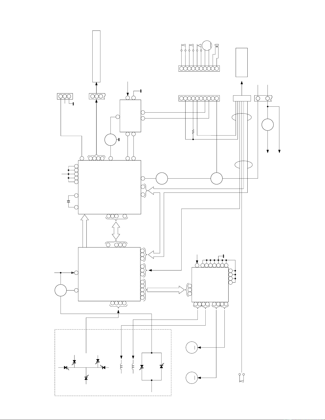
Figure 19 BLOCK DIAGRAM (1/3)
1
2
3
4
5
98
6
7
20
12
13
24
25
30
31
3222
34
35
36
10 11
27
26
28
29
PU-IN SW
XL1
XIN
LD0
FIN2
JP–
CV+
SLC
SL1
FIN1
E
F
TO
FD
SPO
NC
SLD
SL–
SL+
DRF
CL
DAT
CE
VCC1
6
+5V
+5V
PICKUP IN
SW4
FOCUS COIL
TRACKING COIL
M1
DISC
MOTOR
M
M
M2
SLED
MOTOR
PICKUP UNIT
9
IC2
LC78622K
SERVO/SIGNAL
CONTROL
+B1
IC3
M56748FP
DRIVER
IC1
LA9241M
SERVO AMP.
6
9
8
1
5
+B1
( TO IC601 )
RES. CQCK. COIN
SQOUT. RWC. WRQ
~
~
~
CL, DAT, SELIAL CONTROL/CE
Q93
Q51
Q91
SL+. SL–. DRF
7
3
9
8
7
6
5
4
3
2
1
6
5
GND (D)
MECHA UP
GND (D)
DISK NO.
OPEN/CLOSE
GND (D)
M–
M+
GND (M)
9
8
7
6
5
4
3
2
1
CNP10
M
+5V
62
64 45 3623 43
37
31
27
38
39
40
24
25
10
10
265853
10
12
20
32
40
43
44
5352515431302923271615
4144
Q1
+5V
+7.3V
Q52 +7.3V (+B1)
+12V (+B5)
CNP11
REGULATOR
TO MAIN SECTION
IC81
TA7291S
LORDING MOTOR
DRIVER
XOUT
EFMO
EFMIN
CLV+
JP–
CONT2
CONT1
RCHO
RVSS
LVSS
LCHO
VVDD
VDD
LVDD
RVDD
XVDD
SW1
OPEN/CLOSE
SW2
MECHA UP
SW3
DISC No.
M3
LOADING
SOLM2
TO MAIN
SECTION
CNS10
CNP12
6
5
CNP11
6
5
1
3
52
6
5
1
3
52
CNP99
CNP11
CD-C451H
– 20 –
Figure 20 BLOCK DIAGRAM (2/3)
CNS11
1
2
3
FLOUT
FROUT
COUT
RLOUT
FLIN
FRIN
+B4
6
20
19 18
17
16
42
41
40
IC401
QS7777PF
Q-SOUND
31
C-IN
14
34
43
22
7
75
64
65
66
14
15
16
17
1
37
8
6
5
40
41
33
20
48
71
8
2930
52 40
37
38
39
45
41
4243
2
22
23
31
49
50
51
67
68
69
70
72
76
80
56
25
24
23
61
51
60
52
54
59
53
57
55
63
49
30
18
42
6
43
5
42
4
26
6448
2
15
14
20
21
23 22
13
12
4
5
1
3
7
6
8
14
13
19
15
10
12
16
9
8
18
17
7
6
20
5
21
4
4
3
23
2
24
1
17
15
14
11
12
16
18
12
10
13
6
13
10
7
21
22
23
24
20
3
2917
98
5
42
7
5
43
6
21
1
20
11
15 16
1
2
58
5761
R
L
REC
PB MUTE
PB MUTE
MUTING
REC MUTE
MUTING
T1/T2
REC/PB
BAIS
+B5
SWM4
REC RVS
SWM3
REC FWD
SWM5
SWM6
MM1
TAPE
MOTOR
M
JK452
+B4
ICT21
LC72720
RDS
VDDA
VSSA
MW/LW
ANT.
MW/LW
OSC.
L341
BALUN
X352
4.5MHz
IC302
LC72131
PLL(TUNER)
FM IF DET/FM MPX/AM IF
IF
OUT
IC303
LA1832
+B4 CF351 X351
+B4
MPX
PHASE
Q361
SOLENOID
TA MOT H/L
RUN PULSE
DATA
ENEBLE
~
~
SO301
ANTENNA
TERMINAL
MW/AM
ANTENNA
Q129
Q130
BEAT CUT
BAIS
BEAT CUT
R-OUT
L-OUT
C-I
S-IN
+B4
SRS
BALANCE
4CH SP
MAIN STB
CLEAR
MAIN SI
MAIN SO
MAIN SCK
SM
L354
LOW PASS
FILTER
TUNER MUTE
SD
VOLTAGE
REGURATER
+B4
+5V
QT21
–VP
VF2
(AC)
FL701
IC201
IX0222AW
MICROCOMPUTER
+B2
R-MUTE
C-MUTE
S-MUTE
POWER
CAM SW
CLK
CAM SW
TA MOT SW
REC/PB
F.A.S
REC FWD
REC RVS
PB MUTE
T1/T2
BIAS
REC MUTE
S-OUT
VDD
VSS
CL
CE
DI
DRIVER
RUN PULSE
SOLM1
+B5
SOLENOID
SOLENOID
QM03
PHM1
FAS SW
CAM SW
F.A.S
REC RVS
REC FWD
MOTOR
DRIVER
DRIVER
QM02
TA MOT SW
TA MOT H/L
QM05
+B5
SWITCHING
Q117
Q118
Q121
Q122
L
R
VIDEO2VIDEO1
RL
IN
RL
L
R
R
L
L
R
R
L
FRONT
IN
CENTER
REAR
IN
X-BASS
RTINLTIN
VSSD
VDDD
X IN
X OUT
MPX
IN
AMP.
FM +B
DO
CL
DI
CE
XT21
4.332MHz
XT21
VT
T305
T306
T301
T302
CF302
P.B
+B4
REF
T1/T2
NOR/
HIGH
ALC
REC
P.B.
PLAYBACK&RECORD AMP.
IC101
AN7345K
R REC
L REC
POP REDUCE
R
L
R NF
R(T2)
L(T2)
R(T1)
L(T1)
L NF
Q124 Q126
SWITCHINGSWITCHING
DO
CE
CL
DI
CF301
FM FRONT END
FE301
Q360
MUTING
MPX
VCO
CUT
RL
Q353
Q354
MPX
IN
FM/AM
OUT
IF IN
SD
FM MONO/ST
MONO/ST
AM RF IN
AFC
IN
OUT
VR351
FM MUTE LEVEL
AM OSC
REG INOUT VCC
FM IF IN
AMP
FM IF
Q301
FM IF
FM
OSC.
STEREO
AM IN
FM IN
FMOSC
T351
AM IF
GND
OSC.
FM
FM IF
AM RF
IC601
LC75396N
AUDIO PROCESSOR
TAPE 1
TAPE 2
Q128
L103
Q111
Q107
Q108
Q110
Q109
Q103,Q104
Q105,Q106
REC/PBREC
P.B
AC BIAS
P.B
REC/PB
HEAD
L-CH
R-CH
PB HEAD
L-CH
R-CH
ERASE
HEAD
AUX
AUX
TUNER
TAPE
CD
V
O
V
O
T1/T2
H/N
RRRLLL
GRAPHIC EQUALIZER
47
RT-IN
LT-IN
L-OUT
R-OUT
CL
+B4
CL
DATA
DATA
ENABLE
X501
8
18
45
46
23
24
IC501
LV1035M
DOLBY PRO LOGIC
DECORDER
38
35
37
36
42
33
9
31 32
22
34
C-OUT
21
FROM CD UNIT
CNP11
– 21 –
CD-C451H
Figure 21 BLOCK DIAGRAM (3/3)
CNS12
SO801
4
7
1
8
6
2
63 61
64
65
66
23
28
13
16
18
17
1
4
3
2
36
38
37
46
17
35
34
42
43 47
9
XL701
1011
12
31
2
19
21 22
18
1615
1413
14
15
16
17
18
20
31
3348
30
8
29
52
71
54
70
72
80
1
4
6
7
5
8
6
5
7
21
9
10
11
12
13
19
21
53
54
55
24
25
26
27
28
4
5
6
7
8
6
7
7
1
4
8
5
3
28
20
17
31
30
18
42
6
5
7
IC651
NJM4558L
OPE AMP.
SPE1-5
–B1
IC561/562/563
N5M4558L
OPE AMP.
IC562(1/2)
N5M4558L
OPE AMP.
+B4
VF1
(AC)
~
IC701
IX0223AW
MICROCOMPUTER
~
~
Q704
INPUT/OUTPUT
EXPANDER
IC702
BU2092F
~
9
5
~
+B2
+B2
+B2
Q675
Q676
Q603
Q604
+B3
C-IN
S-IN
DOLBY P.L
SRS
BALANCE
4CH SP
+B2
SW701~SW703
SW709~SW716
SW718,719,721,723,724
SW725,726,728~732
SW733,734,736~740
KEY MATRIX
SW704~708
KEY0
KEY5
LED701~LED705
LED706~LED711
VDD
VSS
LCK
CLOCK
DATA
Q705
Q706
ZD701
SYS STOP
RESET
+B6
S-MUTE
POWER
REMOCON
DI
CLK
DO
CE
RX701
REMOTE
SENSOR
REMOCON
TUN SD
TUN SM
TUN MUTE
CLEAR
MAIN SO
MAIN SI
MAIN SCK
MAIN STB
MAIN STB
CLEAR
MAIN SI
MAIN SO
MAIN SCK
SPE IN
+B2
MEMORY
BACK UP
+B5
–VP
–VP
Q701
W
P
UTER
TO CD UNIT
CNP12
CD RES
CD SL–
CD SL+
CD CQCK
CD SQOUT
CD COIN
CD WRQ
CD RWC
CD PUIN
CD DRF
CD O/C SW
CD D.NO
CD U/D
POWER ON/STB
SWITCHING
C-MUTE
R-MUTE
S-MUTE
POWER
Q601 Q602
Q201
–B1
–15V
CENTER
REAR
IN
VOLTAGE
REGURATER
OUT
IN
R
L
R
L
CENTER
OUT
REAR
OUT
VOLUME
VOLUME
RL
Z
ER
L
R
~~~
13
4
8
JK452
REAR-OUT
CENTER
OUT
9
2
5
12
+12V (ANALOG)
+B4
+12V (MOTOR)
VF1(AC)
VF2(AC)
–VP
+B5
VOLTAGE
REGULATOR
VOLTAGE
REGULATOR
VOLTAGE
REGULATOR
+B1
REAR SPEAKER
CENTER SPEAKER
JK700
HEADPHONES
M901
FAN MOTOR
+7.3V
TO CD UNIT
Q820
Q822
Q824
Q825
Q823
Q826
T.F
AC 230-240V 50Hz
L801
CORE
AC POWER
SUPPLY CORD
VOLTAGE
REGULATOR
Q801
Q903
Q901
Q827
Q902
D807
D809
~
D803 ~ D806
ZD801
14
1
2
8
4
3
L-OUT
FRONT
R-OUT
10
15
R-IN
FRONT
L-IN
–B
+B
+B3
IC901
STK40704
POWER AMP.
IC471
NJM4558L
OPE AMP.
D801
F802
T3.15A
L250V
T801
POWER
TRANSFORMER
F803
T3.15A
L250V
F832
T500mA
L250V
F902
T4A
L250V
F901
T4A
L250V
F805
T1.6A
L250V
+
–
+
–
FRONT SPEAKER
SO901
SPEAKER TERMINAL
R
L
3
5
1
7
IC681
NJM4560L
HEADPHONE AMP.
Q905
M
Q671 Q672
Q673 Q674
H/P MUTE
+B1
+B3
+
–
6
7
+B3
Q609
+B2
+5V
+12V
+B5
Q609
VOLTAGE
REGULATOR
CD-C451H
– 22 –
• The numbers 1 to 12 are waveform numbers shown in page 44.
Figure 22 SCHEMATIC DIAGRAM (1/14)
A
B
C
D
E
F
G
H
1
23456
• NOTES ON SCHEMATIC DIAGRAM can be found on page 18.
1
2
3
4
5
5
4
3
2
1
8
7
1
5
4
3
2
1
6
5
4
3
2
8
7
2
3
4
5
6
8
7
2
3
4
5
6
M
M
11
6
5
4
3
2
1
6
5
4
3
2
1
6
5
4
3
2
1
6
5
4
3
2
1
8
7
6
5
4
3
2
1
5
4
3
2
1
2200P
1M
2200P
1M
PD
VR
LD
TR–
TR+
FO+
FO–
GND
PD
VR
LD
TR–
TR+
FO+
FO–
GND
PICKUP UNIT
ACTUATOR
TR–
FO–
FO+
TR+
LD GND
LT0H30M1
C
F
A
B
E
K
LD
MON
1/16
CD MOTOR PWB-E
–
+
–
+
CNP12
C33
0.47/50
C34
0.33/50
R21
22K
R22
22K
D1
1SS133
R37
82K
R26
82K
C13
330P
IC1
LA9241M
SERVO AMP.
R45
4.7K
C
2
0.
0
R38
470
R46
560
C2
0.01
C85
0.001
C1
47/16
R2
1K
C12
0.1
R14
27K
R13
1K
C9
0.047
D2
RL104A
D4
RL104A
C84
0.001
R12
100
C7
0.1/50
C8
0.068
C10
180P
R15
12K
R16
3.3K
C18
0.47/50
R31
1.2K
C26
0.033
R40
5.6K
C24
2.2P
C27
0.001
C30
0.1/50
C31
220/6.3
C32
0.01
R32
10K
R33
1.2K
C19
1/50
C20
47/16
R36
220K
C21
0.0033
R35
220K
D3
RL104A
C11
0.1
R18
15K
R1
22
C35
1/50
C4
0.1/50
C14
0.01
C28
0.1
C29
4.7/50
R17
33K
R24
47K
R23
10K
R25
1.5K
R27
39K
C16
0.0047
R9
100K
R8
15K
C54
0.001
C5
0.033
R10
2.2K
C6
0.033
R11
6.8K
IC3
M56748FP
FOCUS/TRACKING/SPIN/SLIDE DRIVER
C36
100/16
R48
10K
R34
22K
C3
1/50
R19
1K
R20
1K
R30
6.8K
C17
0.001
R29 56K
R28 10K
R42
47K
R44
33K
R43
56K
R41
47K
C15
0.01
R39
1K
C25
27P
Q1
KTA1266 GR
3
21
36
35
34
33
32
31
30
29
28
27
26
25
24
23
22
21
20
19
17
18
16
9
6
15
14
13
12
11
10
8
7
5
4
3
2
1
1
2
3
4
5
6
7
8
9
10
11
12
13
14
15
16
17 18 19 20 21 22 23 24 25 26 27 28 29 30 31 32
33
34
35
36
37
38
39
40
41
42
43
44
45
46
47
48
49505152535455565758596061626364
CD_PUIN
SL_–
SL_+
SP–
SP+
CO IN(DSP)
WRQ(DSP)
RWC(DSP)
CD_GND
TP1
HF
FE1
SLOF
SLOF
FSC
FOSTA
TE
F
E
B
A
K
K
E
B
A
F
K
E
B
A
F
4.2V
1.5V
4.8V
CV+
CV–
SLOF
HFL
TES
TOFF
TGL
JP+
JP–
RFSM
RFS–
SLC
RF
REF
OR
REF
REF
REF
REF
SL+
SL–
SLD
SLEO
SPO
SP–
SPG
SPI
SP
AGND
FE–
FE
FA
FA–
FD–
GEN
GEN
GEN
FD
TO
JP
TD–
TD
TH
TA
REF
JP
REF
TO
REF
REF
REF
REF
REF
REF
REF
REF
REF
REF
REF
SCI
TESI
TE
TE–
TB
F
E
FIN1
FIN2
VCC1
LDS
BH1
PH1
LF2
VR
REFI
VCC2
DRF
CE
DAT
CL
CLK
DEF
SLI
DGND
REF
LDD
RF
REF
REF
FE1
VCR
VCR
VCR
VCR
TGL1
THDL
GL
THD
VCC
DEF
HFL
DRF
CE
CL
SLOF
FSTA
LATOH
TOSTA
FOSTA
S.Q.R
FSTA
8/12CM
LASER
2FREQ
JP+
JP–
CV+
CV–
REF
REF
JP
REF
-
+
EFBAL
FSC
SLOF
JPCLO
FSS
TBC
CNS1B
CNS1A
CNS2B
CNS2A
CNP3A
CNS3B
CNS3A
M1
DISC
MOTOR
M2
SLED
MOTOR
SW4
PICKUP
IN
CNP3
CNP2
CNP1
+B +B
+B
+
–
+
–
+
–
+
–
+
–
+
–
+
–
+
–
+
–
+
–
+
–
+
–
+
–
+
–
+
–
+
–
+
–
+
–
+
–
+
–
+
–
+
–
+
–
+
–
+
–
+
–
+
–
+
–
+
–
+
–
2.5V
2.5V
2.5V
2.5V
2.5V
2.5V
2.4V
2.5V
2.5V
2.5V
2.5V
2.4V
2.5V
2.5V
2.4V
2.4V
0V
2.2V
2.2V
2.5V
2.5V
2.5V
2.5V
2.5V
2.5V
2.5V
0V
2.5V
2.4V
2.5V
2.5V
2.5V
0V
0V
4.8V
0V
0V
4.8V
4.8V
0V
1.5V
2.4V
2.5V
2.4V
0V
2.5V
0V
2.5V
4.8V
0V
2.2V
1V
1V
2.5V
2.5V
4.8V
0V
0V
4V
4V
2.4V
0V
4.2V
4.8V
4.7V
0V
0V
0V
2V
2.5V
2.5V
2V
2V
0V
0V
0V
2V
2.5V
2.5V
0V
2.5V
2.5V
4.7V
0.7V
2.5V
0V
1.8V
2.5V
2.5V
2V
2V
0V
0V
0V
1.8V
2.5V
2.5V
0V
0V
0V
10
12
5
4
3
2
9
6
7
1
8
– 23 –
CD-C451H
Figure 23 SCHEMATIC DIAGRAM (2/14)
7
8 9 10 11 12
2
CNP11
D1
1SS133
C44
100P
C45
100P
C47
100P
C22
220P
C23
0.0027
8
R53
1.2K
C74
220P
C73
220P
R73
390
R74
390
C43
330/6.3
C48
100P
C49
100P
C81
47/16
C57
0.001
D
4
R
L104A
R62 1K
R63 1K
C38
0.01
R61 1K
R57 1K
3
R60
1K
R52
27K
C40
0.047
C39
0.047
R50
680
R90 1K
R91 1K
R89 1K
R83
3.9
C83
0.022
D82
1SS133
D81
1SS133
C72
10/50
C71
10/50
R93
220
C42
15P
C41
12P
C
35
/50
R88 1K
C
28
0
.1
CNP10
R51
3.3M
R42
47K
R44
33K
R39
1K
IC2
LC78622K
SERVO/SIGNAL
CONTROL
C46
100P
C53
0.022
R47
10K
C37
0.022
Q91
KTA1271 Y
Q93
KRC102 M
R87
10K
R86
2.2K
D91
1SS133
R82
6.8K
C82
47/16
L61
0.82µH
C51
100/16
ZD61
MTZJ5.6B
R66
220
R64
22
C52
100/16
Q52
KTC3203 Y
C56
0.022
R72
2.7K
R71
2.7K
C50
0.022
R55
150
R81
2.7K
R85
56 (1/2)
C75
0.001
432987651
1413121110
1
22
1
1
2
3
4
5
6
10
9
8
7
6
5
4
3
2
1
10
9
8
7
6
5
4
3
2
1
3
2
1
CNP99
6
1
2
3
4
5
46
47
49
5660
61
1
13
24
38
37
36
35
34
33
323130292827262523222120191817
16
15
14
12
11
10
9
8
7
6
5
4
3
2
64
63
62
59
58
57
55
54
53
52
51
50
39
40
41
42
43
44
45
48
123456789
R59 1K
R58 1K
Q51
KRC107 M
R80
6.8K
R54
330
12V
6.5V
0V
0V
0V
6.4V
1V
6.5V
6.5V
2.9V
BIM5
FSEQ
EMPH
CONT5
C2F
TEST3
LVSS
MUTEL
MUTER
SBSY
EFLG
UP/DOWN
DISC NO.
OPEN/CLOSE
PUIN SW
SLD–
SLD+
D_GND
DRF (ASP)
RES(DSP)
CQ CK(DSP)
SQ OUT(DSP)
CO IN(DSP)
WRQ(DSP)
RWC(DSP)
UP/DOWN
GND(D)
DISC NO.
OPEN/CLOSE
GND(D)
M+
GND(M)
SOL
GND(D)
CNS10
SW3
DISC NUMBER
CNS5
SW2
MECHA UP
SW1
OPEN
CLOSE
SENSOR
PWB-F
CD SERVO PWB-C
M3 T/T
UP/DOWN
LOADING
LOCK
SOLM2
SOLENOID
0V
12V
CD_LD_M–
CD_LD_M+
R-CH
TO MAIN PWB(2/3)
P32 6-A
CNS11
A_GND
L-CH
D-GND
7.3V
M_12V
6.5V
5.5V
CD_LCH
4.9V
+5V
A_GND
CD_RCH
XL1
16.934MHz
X-TAL
GENERATOR
4M
16M
/RES
/CQCK
COIN
SQOUT
RWC
WRQ
FSX
PW
SFSY
SBCK
TEST11
U-COM
INTERFACE
SUB-CODE
XVSS
XIN
XOUT
XVDD
RVDD
RCHO
RVSS
LCHO
LVDD
NC
TEST4
TEST1
1BIT
DAC
4FS
DIGITAL
FILTER
DOUT
DIGITAL
OUT
ERROR COERECT
FLAG CONTROL
VCO CLOCK
OSC CONTROL
SLICE LEVEL
CONTROL
SYNC-DETECT
EFM DEMODULATE
EXTERNAL
OUTPUT
CLV
DIGITAL SERVO
CONT4
CONT3
CONT2
CONT1
VDD
PCK
JP–
JP+
TGL
TOFF
DEF1
PDO
VVSS
ISET
VVDD
FR
VSS
EFMO
EFMIN
TEST2
CLV+
CLV–
V/P
HLF
TES
SERVO
COMMAND
2KX8
RAM
M
TA1
/CS
TEST5
0V
0V
12V
3
2
1
IC81
TA7291S
LOADING MOTOR DRIVER
TO DISPLAY PWB(2/3)
P32 2-A
CNS12
+B
+B
+B
+B
+B
+B
+B
+B
+B
3
1
2
2.9V
0V
0V
–
+
M–
0V
0V
0V
1.9V
4.8V
0V
0V
2.5V
2.5V
0V
0V
0V
4.8V
0V
0V
0V
0V
0V
0V
4.8V
0V
2.5V
0V
0V
0V
0V
4.8V
2.5V
0V
0V
4.8V
4.8V
2.4V
2.5V
4V
4V
4V
0V
0V
0V
2.4V
0V
2.4V
0V
0V
0V
0V
0V
0V
4.8V
4.8V
0V
2.2V
0V
2.1V
2.2V
4.8V
4.5V
2V
0V
2V
4.5V
0V
0V
CD SIGNAL
CD SIGNAL
11
CD-C451H
– 24 –
A
B
C
D
E
F
G
H
1
23456
• NOTES ON SCHEMATIC DIAGRAM can be found on page 18.
Figure 24 SCHEMATIC DIAGRAM (3/14)
(UJ)
(UJ)
2
1
8
7
6
5
4
3
2
1
22
21
20
19
18
17
16
15
14
13
12
11
10
9
8
7
6
5
4
3
2
1
24
23
22
21
20
19
18
8
7
6
5
4
3
2
1
+B
+B
+B
+B
+B
0V
2
(12.1V)
(1.2V)
12.1V
3
12.1V
(0V)
(0V)
9.4V
0.8V
0V
(0.7V)
0V
0V
0V
(0.7V)
0V
0V
0V
(0.7V)
0V
0V
0V
(0V)
3.9V
0
V
X IN
X OUT
VSS
AOUT
AIN
PD
VDD
FM IN
MW
AM IN
FM
MO/ST
ST IND
IF IN
CE
DI
CL
DO
FM
2
MW+B
1
(CH)
FM MUTE
LEVEL
AM IIF
3
2
1
IC303
LA1832
FM IF DET/
FM MPX/AM IF
FM
DET
FM IF
IN
AM MIX
OUT
AM OSC
IN
AM OSC
OUT
REG
FM
AFC
AM RF
IN
VSM
CUT
AM LOW
STEREO
SD
GND
AM IF
IN
OUT
FM/AM
LOW P
A
FILT
E
FM IF AMP.
LW ANT.
MW ANT.
(CH)
MW
OSC.
3
2
1
C326
18P
(CH)
(CH)
LW OSC.
MW/LW
LOOP
ANTENNA
BALUN
FM
75ohms
ANTENNA
TERMINAL
3
2
1
IF OUT
GND
F OUT
VT
VCC
GND
GND
ANT
R369
82
Q371
KTA1266 GR
C327
680P
D351
1SS1
3
D352
1SS133
R382
150
C380
10/16
R378
82K
R373
1K
R372
1K
R374
1K
R371
1K
C350
0.022
C352
10/16
C351
0.022
R351
5.6K
C399 0 022
C353
0.022
C354
0.022
R393
1K
C364 10/16
C366 0.001
C365 0.022
C363 0.022
C343
33P
VR351
10K(B)
C325
220P
R335
100K
D301
1SS133
CNP301
R349
33
R344
470
R345
4.7K
R301
330
C346
0.022
C345
0.022
C321
100/16
L354
R379
2.2K
C382
15P
C381
12P
(CH)
X352
4.5MHz
C385
0.01
R377
47K
L351
100µH
4
5
R358
8.2K
C342
0.022
R
3
2
7
CF351
C361 0.022
D304
1SS133
C301
0.001
D303
1SS133
L341
C362
3.3/50
Q362
KRA107 M
C393
1/50
R380
1.5K
R381
10K
C394
47/16
SO301
C387
0.022
C392
0.001
L353
1mH
C397
0.022
R346
330
R347
6.8K
C341
0.022
R348
680
FE301
FM FRONTEND
CF301
Q301
2SC380 O
C347
0.022
C328
0.022
R334
5.6K
C334
18P (UJ)
R336
4.7K
R337
470
R324
100K
T305
C324
27P
R333
5.6K
T306
C336
470P
C335
18P
VD301-2
KV1236Z23F
R323
68K
Q303
KTC3199 GR
Q304
KTC3199 GR
C384
0.001
CF302
T301
C322
6.8P (CH)
C333
22P (CH)
C323
0.022
R331
5.6K
C330
10P
T302
C332
0.022
R319
100K
C331
0.047
VD301-1
KV1236Z23F
Q302
KTC3199 GR
D302
1SS133
R352
1K
CF352
T351
C337
0.022
C339
22P
IC302
LC72131
PLL (TUNER)
C338
0.001
C329
33P
C302
0.001
CHASSIS
GND
CHASSIS
GND
CHASSIS
GND
C367
1/50
R350
2.7K
R332
100K
R397
1K
L342
2.2mmH
– 25 –
CD-C451H
Figure 25 SCHEMATIC DIAGRAM (4/14)
7
8 9 10 11 12
12 11 10
987654321
24
23
22
21
20
19
18
17
16
15
14
13
12
11
10
9
7
6
5
4
3
2
1
8
13
12
11
10
18
17
16
15
14
13
12
11
10
9
8
7
6
5
+B
+B
+B
+B
+B
+B
+B
+B
+B
+B
2.6V
(0V)
(0V)
2V
(0V)
5.2V
(3.6V)
0V
(0V)
3.9V
0V
(12.1V)
11.3V
(0V)
11.3V
12.1V
(0V)
(0V)
0.7V
0.7V
0V
0V
0V
0V
VREF
SYR
CE
DI
CL
DO
RDS-ID
SYNC
VDDD
VSSD
XIN
XOUT
FLOUT
VSSA
MPXIN
CIN
T1
T2
VDDA
MO/ST
ST IND
IF IN
AM SIGNAL
FM SIGNAL
TO MAIN PWB(2/3)
P32 5-H
CNP303
SD
SM
R
L
TUN MUTE
A GND
A+12V
DI
CE
DO
CLK
D GND
3
2
1
FM
DET
CU
STEREO
SD
GND
OUT
FM/AM
VCC
IF OUT
PHASE
PHASE
(FM/AM)
MO/ST
R-CH
OUT
MPX
IN
MPX
VCO
L-CH
OUT
(CH)
TPTPTP
(CH)
LOW PASS
FILTER
MUTING
MUTING
TP
1
R
D351
1SS133
R385
5.6K
C391
47/16
R384
5.6K
3
R376
1K
R378
82K
C386
330P
CNP303
R354
3.9K
C399 0.022
0.022
C354
0.022
R393
1K
C358
1/50
ZD351
MTZJ5.1B
RT49
390
RT48
390
CT43
10/16
RT21
100K
RT26
1K
RT51 1K
RT52 1K
RT53 1K
RT54 1K
RT28
1K
RT30
1K
LT22
2.2µH
RT37
220K
RT36
220K
C366 0.001
R356
1K
C369 27P
C373
0.033
C374 0.033
R357 470K
R364
2.2K
L354
85
0
1
R
377
47K
5
1
µH
R363
2.2K
R366
10K
R368
33K
R365
10K
C375
3.3/50
R367
1K
Q353
KTC3199 GR
Q354
KTC3199 GR
X351
456KHz
C368
1/50
R353
270
L352
100µH
CT23
10/16
ICT21
LC72720
RDS DECORDER
C355
22P
C370
1/50
ZDT21
MTZJ5.1B
C357
2.2/50
R355
3.3K
C356
0.001
CF351
C398 100/10
RT32
10K
RT33
56K
QT21
KTC3199 GR
CT37
0.022
RT34
56K
R362
470
C372
1/50
R361
470
C371
1/50
D353
1SS133
R395
47K
R359
1.8K
R360
4.7K
C396
100/10
C395
0.022
Q360
KTA1266 GR
R383
5.6K
R392
390
R391
390
CT24
0.022
CT25
560P
XT21
4.332MHz
CT26
22P
CT29
0.022
CT28
47/10
RT29
1K
LT21
2.2µH
CT21
47/10
CT22
0.022
CT36
0.022
R387
22K
Q361
KRC107 M
MPX PHASE
ZD352
MTZJ3.9B
CT27
22P
C367
1/50
R350
2.7K
RT35
220K
TUNER PWB-H
R370
1K
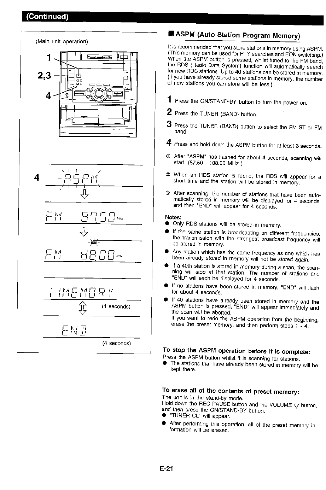
CD-C451H
– 26 –
Figure 26 SCHEMATIC DIAGRAM (5/14)
A
B
C
D
E
F
G
H
1
23456
• NOTES ON SCHEMATIC DIAGRAM can be found on page 18.
7
6
5
4
3
2
1
6
5
4
3
2
1
+B
3
2
1
M
13
12
11
10
9
8
7
6
5
4
3
2
1
3
2
1
+B
+B
24 23 21
20
22
19 18 17
87654321
7
6
5
4
3
2
1
TAPE1
PLAYBACK HEAD
L-CH
R-CH
TAPE1_L
A_GND
TAPE1_R
1
13
TAPE MECHANISM PWB-F
TAPE
SPEED
–
+
H
L
4
1
REC RVS
SOLENOID
F.A.S.
CAM
REC FWD
TAPE
MOTOR
T2_B_FP
PUL
T2_PH_IN
T1_RUN
D_GND
TA_CAM_SW
T2_A_FP
MOT +B
MOT H
MOT L
T2_RUN
T2_B_FP
PUL
T2_PH_IN
T1_RUN
D_GND
TA_CAM_SW
T2_A_FP
MOT +B
MOT H
MOT L
T2_RUN
3
32
2
1
1
+
–
–
+
Hich=T1
–
+
+
–
REC/P.B.
REC/P.B.
REC/P.B.
REC/P.B.
H
M_
G
TAPE2_L2
TAPE2_L1
A_GND
TAPE2_R2
TAPE2_R1
M_GND
ERASE
ERASE
HEAD
HEAD
PWB-H
TAPE2
RECORD/
PLAYBACK
HEAD
R-CH
L-CH
FLEXIBLE
PWB
112K
112K
RM11
8.2K
R
M
1.
2
R
DM02
1SS133
QM03
KTA1271Y
DRIVER
CM01
47/16
QM02
KTA1273
Y
MOTOR DRI
V
QM05
KTA1266GR
DRIVER
CNS101
FWM1
VRM1
3.3K(B)
RM1
2.7K
SWM4
SOLM1
SWM5
CNPM2
SWM6
SWM3
FWM2
MM1
PHM1
WTM1
CNP101
C121
1/50
C101
680P
C102
680P
R102
1K
R101
1K
R118
1K
C
1
2
2
R134
68K
C130
470P
R136
1.8K
R117
1K
C128
3.3/50
R139
560
C129
470P
R135
1.8K
C107
680P
C108
680P
R109
4.7K
Q107
KTC3199 GR
R103
2.2K
R105
3.3K
Q103
2SC1845 F
Q106
2SC1845 F
R107
47K
Q105
2SC1845 F
R104
2.2K
R106
3.3K
Q104
2SC1845 F
R111
15K
R114
10K
Q110
KRC104 M
R113
10K
R115
4.7K
Q109
KTA1266 GR
Q111
KRC104 M
C109
0.022
R123
4.7K
C119
560P
C117
0.033
R121
100K
C111
330P
C113
330P
R140
560
R138
6.8K
R132
15K
C122
1/50
R120
56
C116
47/16
L108
2.2µH
C
1
2
2
R137
6.8K
C127
0.022
R131
15K
R119
56
C115
47/16
L107
2.2µH
C112
330P
C114
330P
R126
5.6K
C120
560P
R124
4.7K
R122
100K
C118
0.033
R125
5.6K
R112
15K
C106
330P
C105
330P
R191
1K
R192
1K
CNP102
R108
47K
Q108
KTC3199 GR
R110
4.7K
CNS102
BI102
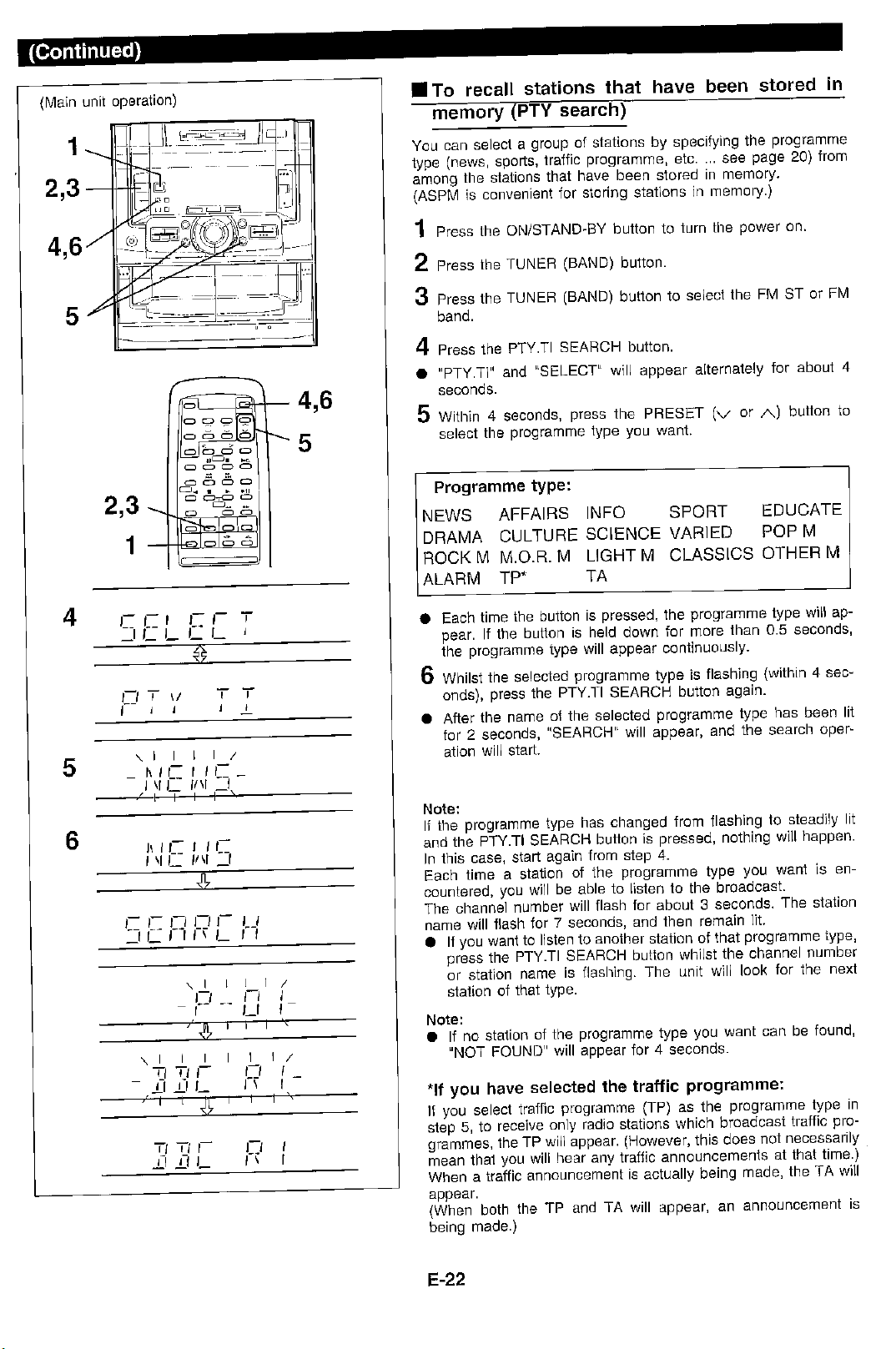
– 27 –
CD-C451H
Figure 27 SCHEMATIC DIAGRAM (6/14)
7
8 9 10 11 12
16
9
3
Z
Y
X
W
20
21
2
6
5
1
15
7
14
13
4
18
8
17
10
12
+B
+B
+B
+B
+B
+B
+B
17
16 15 14 13
121110
98
RECORD SIGNAL
PLAYBACK SIGNAL
TO MAIN
SECTION(2/3)
P32 5/6-A
1-C/E
TO MAIN
SECTION(3/3)
P34 2/3-H
6-A
MAIN PWB-A1(1/3)
TA_CAM_SW
TA_MOT_H/L
T1_RUN
D_GND
T2_A_FP
11
TA_PUL
M_12V
TA_MOT_SW
D_5V
T2_B_FP
T2_RUN
REC_L-CH
REC_R-CH
TAPE_L-CH
TAPE_R-CH
REC/PB
T1/T2
REC_MUTE
PB_MUTE
BIAS
A_12V
A_GND
BEAT_CUT
M_GND
–
+
56K
56K
+
–
Nor/
CrO
2
RIPPLE
Vcc
GND
32
1
MUTING
MUTING
MUTING
MUTING
(P.P)
(ML)
Hich=CHROME
ALC
M_GND
C163
47/16
RM10
1.2K
RM08
10K
RM09
2.2K
QM03
A
1271Y
RIVER
RM07
10
0
1
6
QM02
KTA1273Y
O
TOR DRIVER
RM06
2.2K
RM05
10K
G
R
RM12
33K
RM14
10K
RM16
10K
RM15
10K
RM19
3.3K
RM20
10K
DM03
1SS133
C136
0.039
R146
10K
C140
0.0033
C134
22/25
130
7
0P
R139
560
R143
10K
R144
10K
Q117
2SC2878 A
C143
0.022
C144
0.022
C146
220/10
C147
0.022
C145
22/25
C142
1/50
R140
560
IC101
AN7345K
PLAYBACK AND RECORD/
PLAYBACK AMP.
C141
1/50
R158
470
C133
22/25
6.8K
R168
4.7
R171
4.7K
Q129
KTC3199 GR
Q128
2SC2236 Y
Q126
KRC104 M
SWITCHING
R164
4.7K
Q130
KTC3199 GR
C151
0.027
(ML)
R167
47K
C162
0.047
R170
3.3K
R166
27K
Q124
KTA1266 GR
SWITCHING
L103
1mH
L104
330µH
R160
150
C152
47/16
C156
0.022
Q121
KTC3199 GR
R153
10K
Q122
KTC3199 GR
R154
10K
R142
47
L102
1.8mH
R145
10K
C139
0.0033
L101
1.8mH
R141
47
C135
0.039
Q118
2SC2878 A
R162
47K
C150
0.0082
C161
560P
C110
47/25
R147
10K
R155
120K
R156
120K
C155
100P
R193
220
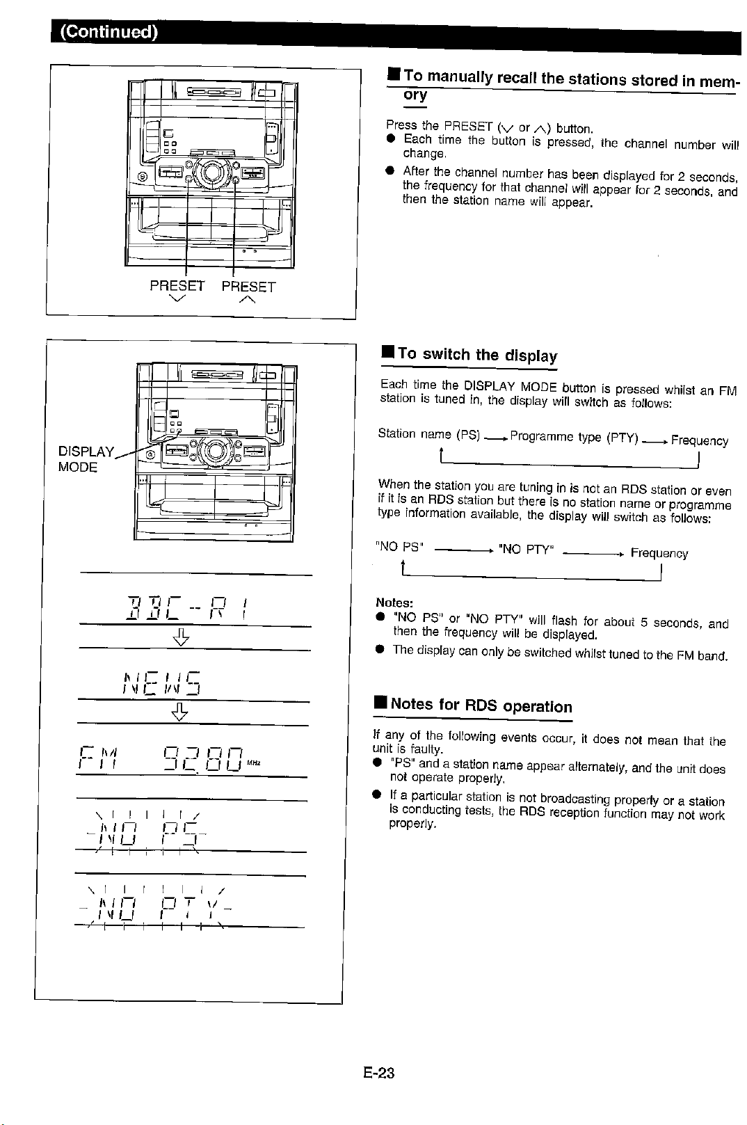
CD-C451H
– 28 –
Figure 28 SCHEMATIC DIAGRAM (7/14)
A
B
C
D
E
F
G
H
1
23456
• NOTES ON SCHEMATIC DIAGRAM can be found on page 18.
MAIN_SCK
MAIN_STB
41 40 37 36 35 34 33 32 31 30
29 28 27 26 25 24 23 22 21 20 19 18 17 16 15 14 13 12 11 10
98765 21
+B
+B
80
73
74
75
76
77
78
79
72
71
70
69
68
67
66
65
64 63 62 61 60
59 58 57 56 55 54 53 52 51 50 49 48 47 46 45 44 43 42
2322212019181716151413121110
987654321
–28.4V
4.8V
–28.4V
DISPLAY PWB-A2
–B
–B
2
21222324
HP RCH
HP_LCH
TUN_MUTE
TUN_SM
TUN_SD
54321
TUN_CLK
TUN_DI
TUN_DO
TUN_CE
F
F
F
F
G11
G10
G09
G08
G07
G06
G05
G04
G03
G02
G01
S01
S02
S03
S04
S05
S06
S07
S08
S09
S10
S11
S12
S13
S14
S15
S16
S17
S18
S19
S20
S21
S22
TUN_SM
TUN_SD
TUN_MUTE
8G
9G
P1
10G
11G
P2
P3
P4
P5
VLOAD
P11
P6
P7
P8
P9
P10
P14
P15
P16
P17
P18
P19
P20
P21
P22
VDD
VSS
REMOCON
SYS STOP
POWER
F_MUTE
P31/TO1
IC
P01/INTP1
P02/INTP2
P03/INTP3/CI0
P71
P72
P70
P00/INTP0/TI0
P
P
P
P16/ANI6
P15/ANI5
P17/ANI7
AVSS
P74
RESET
P24/BUSY
P25/SI0/SB0
P27/SCK0
P23/STB
P22/SCK1
P21/SO1
P20/SI1
P90/FIP2
P80/FIP0
P81/FIP1
P91/FIP3
P92/FIP4
P93/FIP5
P94/FIP6
P113/
FIP21
P114/ FIP22
P115/ FIP23
P127/ FIP33
P116/ FIP24
P117/ FIP25
P120/ FIP26
P121/ FIP27
P122/ FIP28
P123/ FIP29
P124/ FIP30
P125/ FIP31
P126/ FIP32
VLOAD
P97/
FIP9
P96/
FIP8
P95/
FIP7
P105/
FIP15
P104/
FIP14
P102/
FIP12
P100/
FIP10
P101/
FIP11
P103/
FIP13
P112/
FIP20
P110/
FIP18
P106/
FIP16
P107/
FIP17
P111/
FIP19
VDD
P26/SO0/SB1
P73
P30/TO0
VDD
MAIN_SO
MAIN_SI
–B
–B
4G
3G
2G
1G
7G
6G
5G
CLEAR
RESET
P12
P13
FL701
R729
1K
R727
1K
R783
10K
R726
R708 1K
IC701
IX0223AW
SYSTEM MICROCOMPUTER
C702 220/10
C701 0.022
R713 1K
R710 1K
R701 1K
R704 1K
R709 1K
R712 1K
R706 1K
R707 1K
R702 1K
R703 1K
R711 100
R705 1K
R778
100K
Q701
KTC3199 GR
R776
1K
R777
33
C716
47/16
C712
1/50
C734
0.0047
C735
0.0047
JK700
HEADPHONES
C713
1/50
R793
4.7
FM SIGNAL
– 29 –
CD-C451H
Figure 29 SCHEMATIC DIAGRAM (8/14)
7
8 9 10 11 12
+B
+B
+B
+B
+B
+B
+B
18 17 16 15 14 13 12 11 10
987654321
+B
321
+B
+B
+B
+B
+B
+B
+B
+B
+B
45 44 43 4142
40
39
38
37
36
35
34
33
32
31
30
29
28
27
26
25
2423222120
0V
0V
0V
0V
4.8V
0V
5V
0V
0V
TO MAIN PWB(2/3)
P33 7-H
CNP701
123456789
101112131415161718192021222324
VF1
–VP
VF2
POWER
F_MUTE
M_12V
D_GND
D_5V
MAIN_STB
CLEAR
MAIN_S1
MAIN_S0
MAIN_SCK
TUN_CLK
TUN_DI
TUN_CE
TUN_DO
A_GND
HP_SW
HP_RCH
HP_LCH
TUN_MUTE
TUN_SM
TUN_SD
DISPLAY PWB-A3
3
1
DISC 1
DISC 2
DISC 3
DISC
SKIP
OPEN
/CLOSE
31
TIMER
/SLEEP
CLOCK
ON/
STAND-BY
REV
REW/
PRESET
DOWN
VOLUME
DOWN
EQUALIZER
/DEMO
REVERSE
MODE
VOLUME
UP
X-BASS
STOP FWD
FF
PRESET UP
REC
PAUSE
DOLBY
PRO LOGIC
/BYPASS
CENTER
MODE
/NORMAL
CENTER
MODE
/PHANTOM
TAPE
VIDEO
/AUX
EON
DISPLAY
MODE
ASPM
PTY./TI
SEARCH
TUNER
/BAND
TUNING
UP/TIME
MEMORY
/SET
TUNING
DOWN
/TIME
BEAT
CANCEL
TAPE 1 EDIT
CD/TAPE 1
EDIT
CD
Q5
Q6
Q7
Q8
Q9
Q10
Q11
OE
VDD
VSS
DATA
CLOCK
LCK
Q0
Q1
Q2
Q3
Q4
32
1
TUN_SM
TUN_SD
POWER
F_MUTE
P32/TO2
P31/TO1
P02/INTP2
P03/INTP3/CI0
P33/
TI1
P34/TI2
P35/PCL
P36/BUZ
VSS
XT2
P04/XT1
AVREF
AVDD
P10/ANI0
P11/ANI1
P12/
ANI2
P13/
ANI3
P16/ANI6
P15/ANI5
P14/ANI4
P17/ANI7
AVSS
P37
P30/TO0
DI
CE
CL
X1
X2
VSS
AVREF
AVDD
KEY-0
KEY-1
KEY-2
KEY-3
XT2
P04
5V BACK UP
C729
47/16
R749
10K
CNS701
SW707SW708
RD07
12K
SW706
RD05
3.9K
SW705
RD04
2.2K
SW704
RD06
5.6K
FW701
FW701-1
FW701-2
RD30
1.2K
RD29
1K
SW734SW733
RD22
1K
SW726
RD23
1.2K
SW725
RD24
1.8K
LED711
333GTH-2
Q–SOUND
VIRTUAL
PROLOGIC
LED709
333GTH-2
LED707
333GTH-2
LED706
333GTH-2
LED708
333GTH-2
LED710
333GTH-2
R742
820
R743
820
R744
820
D708
1SS133
C708
0.01
D706
1SS133
R766
100K
L701
100µH
R728
10K
R727
1K
R783
10K
R726
1K
R
R718 1K
R722 1K
R720 1K
R717 1K
R716 1K
R721 1K
RD35
12K
RD32
2.2K
RD33
3.9K
SW739
SW737
RD34
5.6K
RD20
5.6K
SW701
SW711
SW719
RD17
1.8K
SW710
SW730
SW729
SW728
RD25
2.2K
RD26
3.9K
RD02
1.2K
SW721
RD21
12K
RD11
2.2K
RD18
2.2K
RD16
1.2K
RD08
1K
SW714SW713
SW709
C702
220/10
C701 0.022
R713 1K
R714 1K
R715 1K
C704
18P
C703
15P
XL701
4.19MHz
R719 1K
R712 1K
RD03
1.8K
SW703
RD14
12K
SW716
RD28
12K
SW732
SW731
SW738
SW740
RD27
5.6K
RD13
5.6K
SW715
RD09
1.2K
RD10
1.8K
RD19
3.9K
SW724
SW723
RD01
1K
SW702
SW718
RD12
3.9K
SW712
RD31
1.8K
SW736
R736 8.2K
R735 8.2K
R733 8.2K
R732 8.2K
R731 8.2K
R734 8.2K
R741 1K
R740 1K
R739 1K
R737 1K
R772
1K
R771
100
Q706
KTC3199 GR
Q710
2SD468C
R765
3.3K
D705
1SS133
R773
100
C709
100/10
Q704
KRC102 M
R774
150
R792
22
R790
100
D709
1SS133
D707
1SS133
ZD701
MTZJ3.9B
C710
220/10
LED701 333GTH-2 PLAY
LED702 333GTH-2 FF
LED703 333GTH-2 STOP
LED704 333GTH-2 REW
LED705 333GTH-2 REV
IC702
BU2092F
INPUT/OUTPUT EXPANDER
R770
1K
R768
10K
R767
82
Q705
KTC3199 GR
R769
10K
RX701
R775
2.2K
R791
1.2K
C733
10/16
C731
47/25
ZD710
MTZJ6.2C
C732
0.022
C715
0.022
R738 1K
R763
1K
C706
0.01
C707
3.3/50
RD15
1K
R781 10K
R780 1.8K
R779 10K
C730
0.022
C726
C726-C721:150P
C725
C724
C723
C722
C721
FLAT CABLE(263)
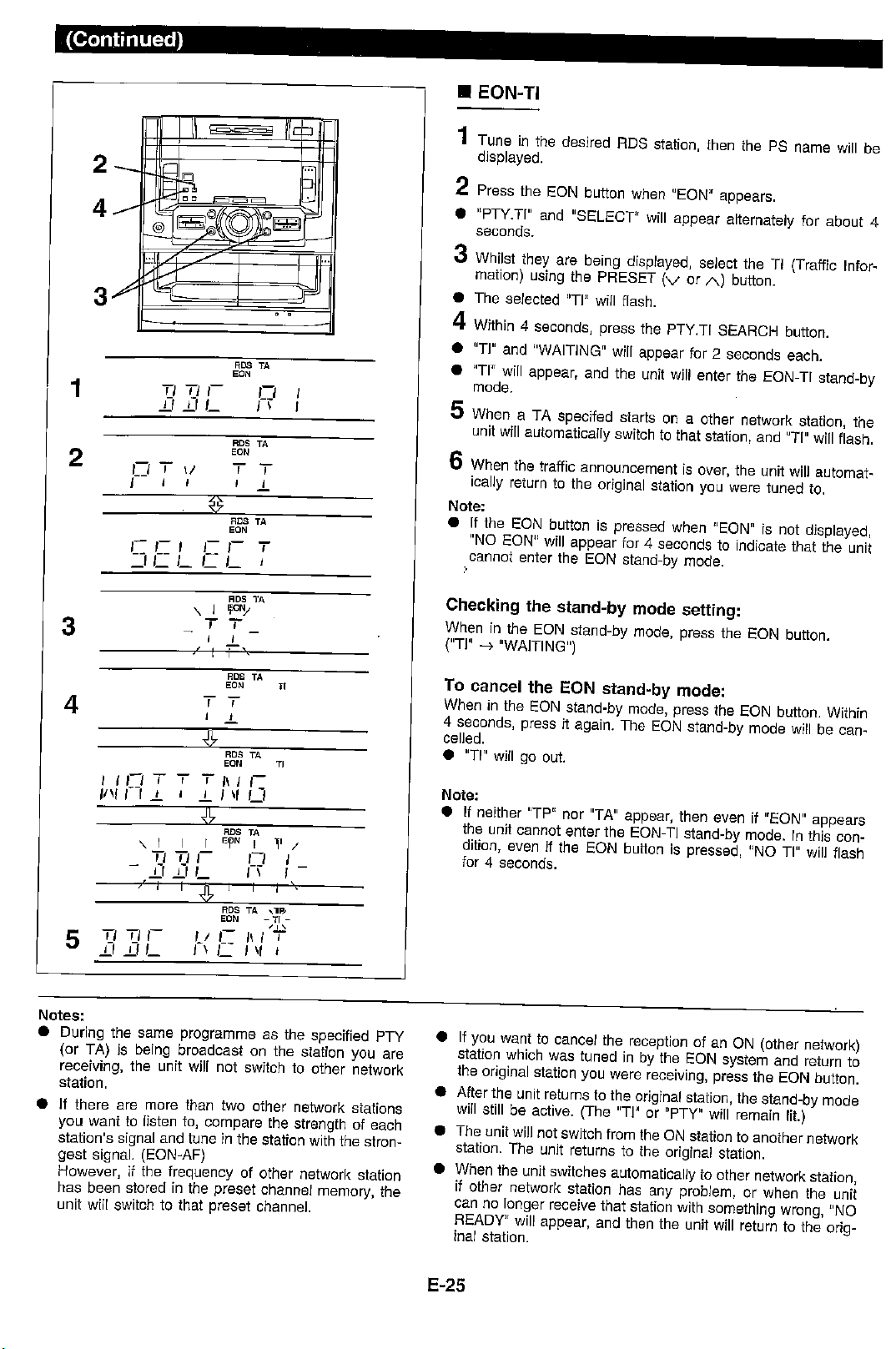
CD-C451H
– 30 –
A
B
C
D
E
F
G
H
1
23456
• NOTES ON SCHEMATIC DIAGRAM can be found on page 18.
Figure 30 SCHEMATIC DIAGRAM (9/14)
C825
22/25
Q826
KTC3199 GR
Q824
2SD2012
Q823
2SD2012
R825
33
C827
47/25
R829
1K
R826
33
IC901
STK40704
POWER AMP.
C910
2200/50
C909
2200/50
C904
10/50
C911
100/50
C826
47/25
Q825
KTC3199 GR
R912
100
R913
100
R915
220K
R918
470
C917
47/50
C916
15P
R917
56K
R922
470
R921
10K
R923
56K
C924
15P
Q902
KRC107 M
Q903
KRC10
7
R932
18K
C923
120P
C915
120P
R924
1K
R916
1K
C907
10/50
C912
100/50
C918
47/50
R836
22K
C824
0.022
R837
22K
R820
47
D822
RL104A
D823
RL104A
C823
47/25
Q822
KTC3199 GR
R824
560
Q820
2SD2012
R838
10K
C831
10/50
C820
0.022
R905
1K
C903
1/50
R907
1K
C902
220P
R902
68K
R901
15K
C901
1/50
R903
15K
C905
220P
R904
68K
Q901
KTA1268 GR
R910
2.2K
R914
15K
R911
10K
C977
1000/6.3
R962
820
D902
1SS133
CNP803
POWER PWB-B
C828
47/25
ZD822
MTZJ13C
R835
560
R827
1K
R828
33K
D824
1SS133
C829
4700/25
CHASSIS
GND
C802
100/35
C803
R
2
ZD801
R801
12K
D804
RL104A
D803
RL104A
R802
220
20
19
18
17
16
15
14
13
12
11
10
9
8
7
6
5
4
3
2
1
151413121110
987654321
R963
820
Q827
KRA107M
D820
1SS133
+B
–VF
+B2
+B
+B
VF1
VF2
GND
–Vcc
–Vcc
+Vcc
Ch1
Ch2
Ch1
Ch2
Out
Out
CNS803
H:ON
L:OFF
2 Ch
30.6V
30.7V
30V
0V
0V
0V
0.3V
3.8V
12.4V
13V
18.2V
13.3V
13V
18.4V
11.6V
12.3V
12.4V
18.4V
6.9V
7.5V
7.6V
8.2V
18.4V
18.4V
3
2
1
32
1
P33 12-G
TO MAIN PWB(2/3)
FRONT_R
FRONT_L
A_GND
STANDBY
7.3V
(CD)
CD_GND
D_GND
A_GND
M_GND
+12V (M)
+12V (A)
VF1
–VP
VF2
+12V (M)
–15V
POWER
3
2
1
F832
T500mA L 250V
–
–B
+
+
–
–0.1V
–0.1V
–32V
–0.1V
–0.1V
33.6V
–33V
0V
0V
0V
0V
35.4V
–35.4V
–35.4V
0V
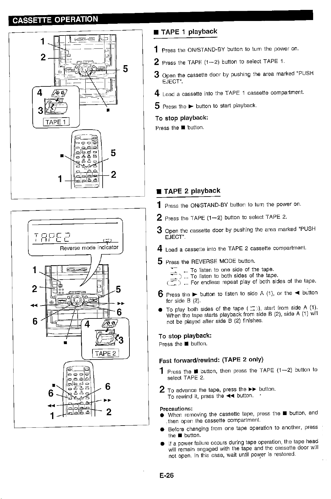
– 31 –
CD-C451H
7
8 9 10 11 12
Figure 31 SCHEMATIC DIAGRAM (10/14)
CNS801
CNP801
R969
68
(1/2W)
7
M
Q903
KRC107 M
C935
0.1
(ML)
C934
0.1
(ML)
R934
4.7
R937
4.7
C937
0.1
(ML)
C936
0.1
(ML)
R965
4.7K
R964
4.7K
Q905
KTC3199 GR
C978
47/50
D903
1SS133
R968
1K
M901
FAN MOTOR
R967
68K
R966
15K
C979
10/50
CNP804
F902
T4A L 250V
F901
T4A L 250V
C817
4.7/50
R805
100
C813
100/50
D809
RL104A
D808
RL104A
D807
RL104A
C802
100/35
C811
47/50
R806
2.2K
Q801
KTA1266 GR
C804
47/50
C803
47/50
R803
220
C812
100/50
ZD802
MTZJ30B
ZD801
MTZJ6.2A
12K
4
0
4A
D805
RL104A
D806
RL104A
0
3
1
04A
220
C805
0.047
(ML)
C806
0.047
(ML)
D801
TS6B04GM-1
C807
0.22
C808
0.22
D827
1SS133
R807
10K
CNP802
CNS802
T801
POWER TRANSFORMER
9
8
7
6
5
4
3
2
1
9
8
7
6
5
4
3
2
1
1
22
1
2
1
2
1
R948
6.8
L903
0.29µH
L901
0.29µH
C957
0.022
C961
0.001
C962
0.001
C958
0.022
R947
6.8
C955
0.022
C956
0.022
R945
6.8
C951
0.022
C952
0.022
R943
6.8
C947
0.022
R972
68
C970
0.001
R973
68
C972
0.001
C948
0.022
+B
1
2
3
4
M
TF801
R-CH
CHASSIS
GND
L-CH
FRONT
6 OHMS
MIN.
F805
1.6A 250V
F802
T3.15A L 250V
F803
T3.15A L 250V
CNS804
+
6.4V
0V
0V
35.3V
–35.3V
.
4V
–28.9V
–28.3V
–34.9V
SO801
INPUT
AC230-240V/
50Hz
AC POWER
CORD
SO901
SPEAKER
TERMINAL
L801
CORE
FM SIGNAL
When Serving, pay attention
as the area enclosed by this
line ( ) is directly
connected with AC main
voltage.
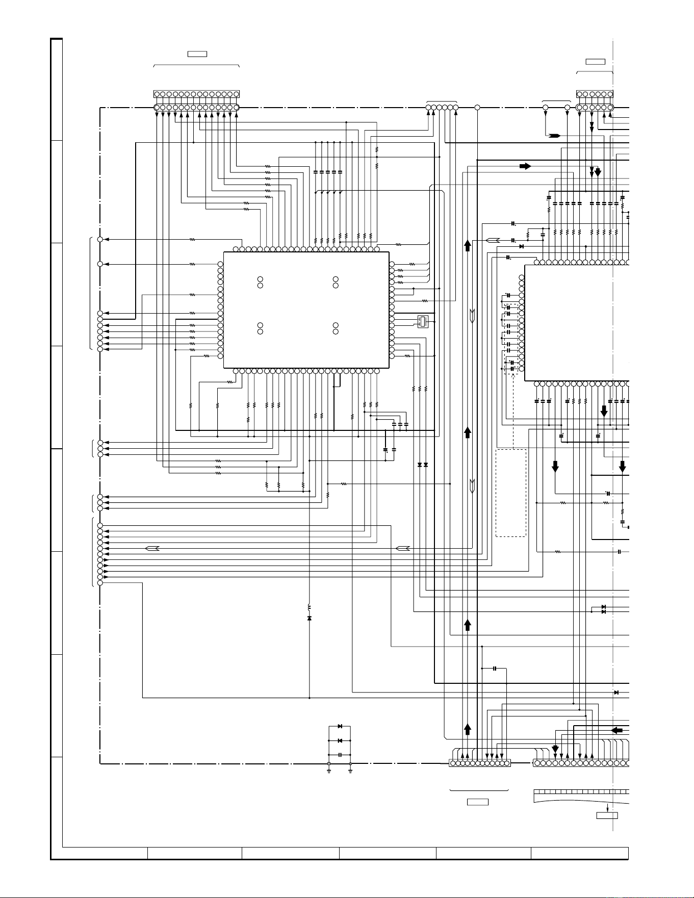
CD-C451H
– 32 –
A
B
C
D
E
F
G
H
1
23456
• NOTES ON SCHEMATIC DIAGRAM can be found on page 18.
Figure 32 SCHEMATIC DIAGRAM (11/14)
R251 1K
R253
1K
R250 1K
R249 1K
R254
1K
R276
47K
C632
0.015 (ML)
R277
1K
C609 0.22
C607 0.22
C605 0.22
C603 0.22
C601 0.22
C602 0.22
C604 0.22
C606 0.22
C608 0.22
C610 0.22
C643 0.047
(ML)
C644 0.047
(ML)
R244
1K
R217 1K
C652
0.1(ML)
C651
0.1(ML)
R
2
R
2
C
3
C666
2.2/50
R
6
2.
2
R661
47K
R660
47K
R615 1K
R610 1K
R604 1K
R230 1K
R213 1K
R214 1K
R232
1K
R215 1K
R218 1K
R258
1K
R262 12K
R261 1K
R256
1K
R228 1K
R243 1K
R202
1K
R260 1K
R259 1K
R237
1K
R225
1K
R224
1K
R220 1K
R233
1K
R242 1K
R271
1K
R221 1K
R227
1K
R226
1K
XL201
4.19MHz
R216 1K
R222 1K
R229 1K
C203 150P
C204 150P
C206 0.001
C205 150P
R280
10K
C207 150P
R263
1K
C615
1/50
C616
1/50
R274
10K
R257
1K
R272
10K
R219
10K
R206 1K
R205 1K
R210 1K
R212
1K
R211 1K
R207 1K
R209 1K
R208 1K
D202
1SS133
R618 1K
R616 1K
R614 1K
C630
0.027 (ML)
C636
0.0047 (ML)
C612
47/16
C614
100P
C628
0.22/50
C626
0.1/50
C624
0.22/50
C638
1/50
C645
10/50
R611 1K
R606 1K
C634
0.0022 (ML)
C646
10/50
D601
1SS133
R613 1K
R620
2.2K
R
2
.
R658
2.2K
C641
2.2/50
C642
2.2/50
C
6
4
7
C640
10/50
C647
47/16
C648
47/16
C649 47/16
R619 1K
R602 1K
R608 1K
R617 1K
R612
33K
80
123456789
10 11 12 13 14 15 16 17 18 19 20 21 22 23 24
64 63 62 61 60 59 58 57 56 55 54 53 52 51 50 49 48 47 46 45 44 43 42 41
79
78
77
76
75
65
66
65
66
79
80
67
68
69
70
71
72
73
74
25
26
27
28
29
30
40
39
40
39
26
25
38
37
36
35
34
33
32
31
1
2
3
4
5
6
7
8
9
10
11
12
13
14
15
16
17 18 19 20 21 22 23 24 25 26 27 28 29 30 31 3
2
64 63 62 61 60 59 58 57 56 55 54 53 52 51 50 4
9
C618
1/50
R279
10K
R235
10K
R234
10K
R240
10K
R241
1K
D557
1SS133
D558
1SS133
C570
0.001
LUG1
D209 1SS133
D210 1SS133
C250
220P
C251
220P
C252
220P
C202
0.022
C201
220/10
R264 1K
R203
1K
R238
1K
R247 1K
R246 1K
R245 1K
L201
100µH
D201
1SS133
9
101112
8
7
6
5
4321
9
101112131415161718192021222324
CNS303
C199
100P
CNS1
1
12 3456
12 3456
BI601
21
20
13 14 15 16 1917 18
BI201
CNS12
I
J
K
L
M
N
O
10
11
12
B
C
D
E
F
G
H
3
4
1
2
5
6
7
8
9
D604 1SS
1
D608
1SS133
123456978
1011121314
123456978
1011121314
CHASSIS
GND
TO TAPE MECHANISM
CHASSIS
M-12V
M-GND
T2-RUN
T1-RUN
D-5V
TO MAIN
SECTION(1/3)
P27 12-D
TA-CAM-SW
UP/DOWN
DISK NO
OPEN/CLOSE
PUIN SW
SLD–
SLD+
D-GND
DRF(ASP)
RES(DSP)
CQ CK(DSP)
SQ OUT(DSP)
CO IN(DSP)
WRQ(DSP)
RWC(DSP)
TO CD SERVO PWB
P23 7-G
CNP12
CNP11
P23 12-C
T2 RUN
T1 RUN
CD-DRF
D-GND
CD-PUIN
MAIN-STB
CLEAR
MAIN-SI
MAIN-SO
MAIN-SCK
T2-A-FP
T2-B-FP
PB-MUTE
T1/T2
TO MAIN SECTION(1/3)
P27 12-A to H
TO MAIN SECTION(1/3)
P27 12-A to H
TO MAIN SECTION(3/3)
P34 2/3-H
TO MAIN SECTION(3/3)
P34 2/3-H
BEAT-CUT
D-GND
BIAS
REC-MUTE
REC/PB
CD SL+
CD SL–
CD RES
CD SQOUT
CD COIN
CD CQCK
VDD
CD RWC
CD WRQ
P74
P73
AVSS
RESET
P26/SO0/SB1
P25/SI0/SB0
P24/BUSY
P23/STB
P17/ANI7
P16/ANI6
P15/ANI5
P14/ANI4
P21/SO1
P20/SI1
P93/FIP5
P22/SCK1
P90/FIP2
VDD
P27/SCK0
P80/FIP0
P81/FIP1
P94/FIP6
P92/FIP4
P91/FIP3
NC CD MUT
REC-MUTE
P.B.MUTE
GND
T1/T2
BIAS
T2 BFP
T2 AFP
REC/P.B.
NC
NC
VLOAD
P113/FIP21
P112/FIP20
P110/FIP18
P106/FIP16
P105/FIP15
P107/FIP17
P111/FIP19
P96/FIP8
P95/FIP7
P101/FIP11
P103/FIP13
P102/FIP12
P100/FIP10
P104/FIP14
P97/FIP9
NC
NC
NC
NC
NC
NC
IC201
IX0222AW
SYSTEM MICROCOMPUTER
P33/TI1
P12/ANI2
P10/ANI0
AVDD
AVREF
P04/XT1
X1
P31/TO1
VSS
X2
P36/BUZ
P35/PCL
P34/TI2
P32/TO2
P11/ANI1
P13/ANI3
XT2
P37
SPE4
SPE3
SPE2
SPE1
C-MUTE
R-MUTE
MIC
SYS MUTE
NC
TA-CAM-SW
SPE5
TA MOT SW
TA SOL
F/R SPEED
VSS
CD U/D SW
CD D.NO. SW
CD O/C SW
VDD
POWER
CLK
DATA
ENEBLE
P126/FIP32
P125/FIP31
P30/TO0
P03/INTP3/CI0
P116/FIP24
P117/FIP25
P115/FIP23
P02/INTP2
P71
P70
P122/FIP28
P123/FIP29
VDD
P72
P121/FIP27
P127/FIP33
SP-
@
DET
P124/FIP30
P120/FIP26
P114/FIP22
D-GND
P00/INTP0/TI0
T2 CrO2
P01/INTP1
NC
RLY DRV
NC
NC
IC
CD-O/C
CD-D-NO
CD-U/D
REC-R-CH
REC-L-CH
A-12V
D_5V
TA-MOT-H/L
TA-PUL
TA-MOT-SW
QS_BYP_AR
QS_MO
QS_AC
MAIN-SO
MAIN-SI
MAIN-STB
MAIN-SCK
CLEAR
TUN-SM
TUN-SD
TUN-MUTE
TUN-DI
TUN-DO
TUN-CLK
TUN-CE
TUN-SM
HP-LCH
HP-RCH
A-GND
HP-SW
TUN-SD
TUN-R CH
TUN-L CH
TUN-MUTE
A-GND
A-12V
TUN-DI
TUN-CE
TUN-DO
TUN-CLK
D-GND
MAIN-STB
CLEAR
MAIN-SI
MAIN-SO
MAIN-SCK
TO
CNS701
CNP303
P33 9-H
TO TUNER PWB
R-MUTE
C-MUTE
IC601
LC75396N
AUDIO PROCESSOR
RTIN
RF1C1
RF1C2
RF1C3
RF2C1
RF2C2
RF2C3
RF3C1
RF3C2
RF3C3
RF4C1
RF4C2
RF4C3
RF5
RTOUT
RFIN
RFCOM
RFOUT
RRIN
RRIN
CIN
RRCOM
RROUT
RVREF
VREF
CL
R2
R3
R4
R5
RINVIN1
RSELO
M-12V
7.3V
D-GND
L-CH
A-GND
R-CH
TAPE-RCH
TAPE-
@
LCH
TO MAIN
SECTION(1/3)
P27 12-D
TO
CD SERVO PWB
LVREF
CE
DI
VSS
COUT
LRCOM
CIN
LFOUT
LFCOM
L
T
L
L
L
L
L
L
L
L
L
L
L
L
LSELO
LINVIN1
L5
L4
L3
L2
L1
VDD
R1
+B
+B
+B
+B
+
+B
+B
+B
D-GND
NC
CLK
DATA
ENEBLE
RTIN
LTIN
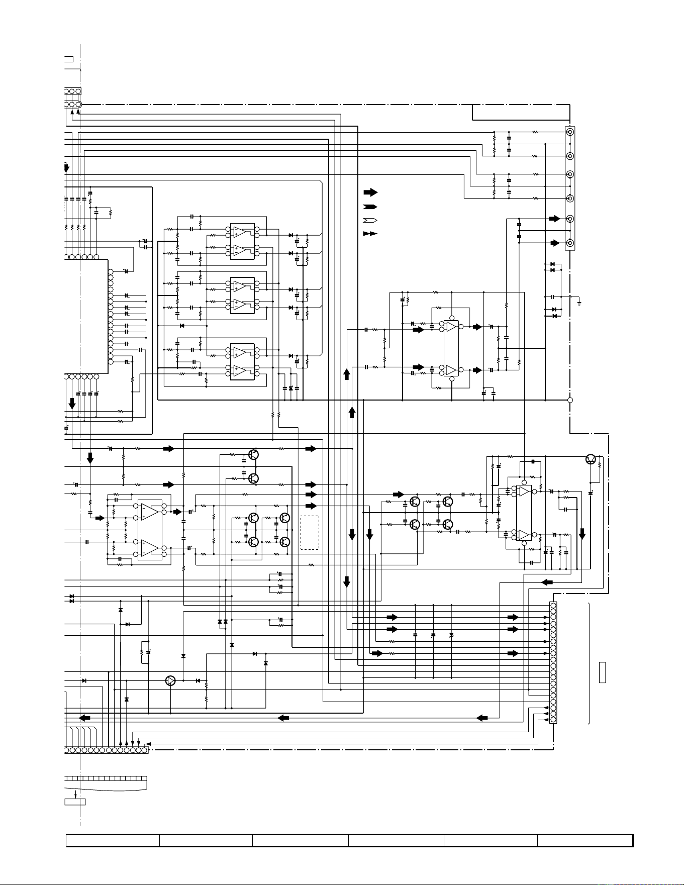
– 33 –
CD-C451H
7
8 9 10 11 12
Figure 33 SCHEMATIC DIAGRAM (12/14)
FM SIGNAL
RECORD SIGNAL
PLAYBACK SIGNAL
CD SIGNAL
D541
1SS133
D540
1SS133
C617
1/50
C677
0.022
R678
10K
R677
10K
R673
2.2K
R676
2.2K
C679
0.001
C678
0.001
Q676
Q675
Q603
R482
100K
R481
100K
R474
100K
R473
100K
R484
1K
R483
1K
C660
2.2/50
R642
22K
R641
22K
C659
2.2/50
C609 0.22
C607 0.22
C605 0.22
C603 0
C643 0.047
(ML)
C665
22/50
D204
1SS133
R624
22K
D605
1SS133
D609
1SS133
C210
22/25
R266
22K
C664
0.001
Q602
KTC3199 GR
C663
0.001
R647
2.2K
R646
2.2K
C657
0.022
Q601
KTC3199 GR
R639
330
R638
330
R645
2.2K
Q604
Q604,Q603
Q675,Q676
:KTC3199 GR
C662
0.001
R644
2.2K
R662
3.9K
R663
3.9K
C658
0.022
C661
0.001
C652
0.1(ML)
R632
6.8K
R630
8.2K
C651
0.1(ML)
R627
2.2K
R633
6.8K
R634
100K
R626
2.2K
R631
8.2K
R635
100K
C656
330P
C655
330P
R637
8.2K
R636
8.2K
R628
47K
R629
47K
C667
2.2/50
C666
2.2/50
R659
2.2K
R661
47K
R615 1K
C564
2.2/50
C561
0.022
R561
15K
C555
0.0068
R559
22K
R555
56K
D554
1SS133
R565
680K
R572
2.2M
C562
0.022
C565
2.2/50
R551
10K
R554
18K
R556
33K
R571
220K
R562
390K
C567
2.2/50
R552
12K
R569
220K
C553
0.0027
C560
0.0082
C552
680P
R558
68K
ZD551
MTZJ6.2C
C569
0.022
C563
0.022
R580
100K
R577
100K
R576
100K
R578
100K
R579
100K
C209
47/25
ZD201
MTZJ13C
C208
0.022
C676
330/16
R654
27K
R653
1.8K
R652
1.8K
C672
390P
C673
390P
C485
470P
C483
470P
R657
27K
R656
27K
C481
47/25
R489
100K
R477
15K
R475
3.9K
R476
3.9K
R478
15K
7
6
5
3
2
1
C476
470P
C475
470P
R472
2.2K
R471
2.2K
C474
47/16
C473
47/16
D203
1SS133
R265
4.7K
D
202
SS133
D205
1SS133
R252
22K
Q201
KRC104 M
R575
330
R574
330
C645
10/50
R611
1K
C633
0.0022 (ML)
C637
1/50
C627
0.22/50
C639
10/50
C629
0.027 (ML)
C613
100P
R621
2.2K
C557
270P
C568
2.2/50
R563
470K
D551
1SS133
R570
220K
R568
220K
R553
12K
C559
0.0027
R564
390K
D556
1SS133
D552
1SS133
D555
1SS133
R566
2.2M
D553
1SS133
R573
560K
C554
0.0082
C556
0.0068
R567
270K
R557
39K
C558
680P
C566
2.2/50
C551
270P
R560
470K
C641
2.2/50
R622
470K
R625
470K
C635
0.0047
(ML)
C611
47/16
R623
470K
C625
0.1/50
C623
0.22/50
R669
33K
C647
47/16
C631
0.015 (ML)
R619 1K
R617 1K
33
2
72829303132
5
45352515049
34
35
36
37
38
39
40
48
47
46
45
44
43
42
41
1
4
8
7
2
3
5
6
8
4
8
1
7
4
2
3
5
6
19
15
13
9
8
7
5
4
2
20
18
17
16
14
12
11
10
6
3
1
2
3
9
1011121314
8
7
6
5
4321
R651
1.8K
R650
1.8K
C671
390P
C670
390P
C674
0.022
CHASSIS
GND
D607
1SS133
D606
1SS133
CNS11
456
456
BI601
R655
27K
6
5
4
8
9
7
3
2
1
C688
220P
C684
47/16
C683
47/16
R698
22K
R697
22K
R697
22K
R601
330
R603
330
R671
2.2K
R672
2.2K
C696
0.001
C695
0.001
Q672
KTC3199 GR
Q671
KTC3199 GR
C698
0.001
C697
0.001
R674
2.2K
R675
2.2K
R680
22K
R699
22K
Q674
KTC3199 GR
Q673
KTC3199 GR
C699
47/25
Q609
KTC3199 GR
R679
220
C685
220P
R682
2.2K
R695
100K
R689
1K
C691
47/25
R686
1.5K
R690
1K
R685
1.5K
C687
47/25
7
6
5
3
2
1
R684
100K
R696
100K
R683
100K
R681
2.2K
C682
0.047
(ML)
C681
0.047
(ML)
8
4
D610
1SS133
D611
1SS133
R648
22K
C668
22/50
R649
22K
C669
22/25
D604 1SS133
D608
1SS133
D206
1SS133
D207
1SS133
D208
1SS133
R487
100K
C480
2.2/50
C479
2.2/50
C484
0.022
C471
0.047
C472
0.047
C490
330P
C488
330P
C482
47/25
R693
47
R691
2.7K
C680
220P
R694
47
R692
2.7K
C692
47/25
C694
0.022
C693
47/25
C690
100P
R688
5.6K
C686
220P
C689
100P
R687
5.6K
1
CNP701
1
4
8
7
2
3
5
6
1
4
8
7
2
3
5
6
A
R665
330
R666
330
P
11
1
2-C
M-12V
MAIN-SO
D-5V
D-GND
S MUTE
POWER
MAIN-SI
MAIN-STB
MAIN-SCK
CLEAR
TUN
-
CLK
MAIN-STB
CLEAR
MAIN-SI
MAIN-SO
MAIN-SCK
TO DISPLAY PWB
CNS701
P29 7-H
–VP
VF1
VF2
N
E
SSOR
M-12V
7.3V
D
-
GND
O
V
O PWB
LVREF
COUT
LRCOM
CIN
LFOUT
LFCOM
LFIN
LTOUT
LF5
LTIN
LF1C1
LF1C2
LF1C3
LF2C1
LF2C2
LF2C3
LF3C1
LF3C2
LF3C3
LF4C1
LF4C2
LF4C3
LSELO
LINVIN1
L5
L4
L3
L2
IC651
NJM4558L
OPE AMP.
IC561
NJM4558L
OPE AMP.
IC563
NJM4558L
OPE AMP.
IC562
NJM4558L
OPE AMP.
MAIN PWB-A1(2/3)
IC471
NJM4558L
OPE. AMP.
VIDEO-1 IN
VIDEO-2 IN
JK452
R-CH
L-CH
SURROUND O
U
CENTER OUT
R-CH
L-CH
IC681
NJM4560L
HEADPHONE AMP.
A-12V
+B
+B
+B
+B
+B
+B
+B
+B
+B
+B
–B
–B
–B
–B
+B
A-GND
–15V
POWER
CENTER
STBY-HI/OPE-LOW
REAR OUT
FRONT-R
A-GND
FRONT-L
VF2
-VP
VF1
A-12V
M-12V
M-GND
A-GND
D-GND
CD-GND
CD-+B
CNS803
TO POWER PWB
CNP803
P30 1
-
F
NC
SPE1
SPE5
SPE4
SPE2
SPE3
FLAT CABLE(263)
A-GND
TO MAIN SECTION(3/3)
P34 6-A
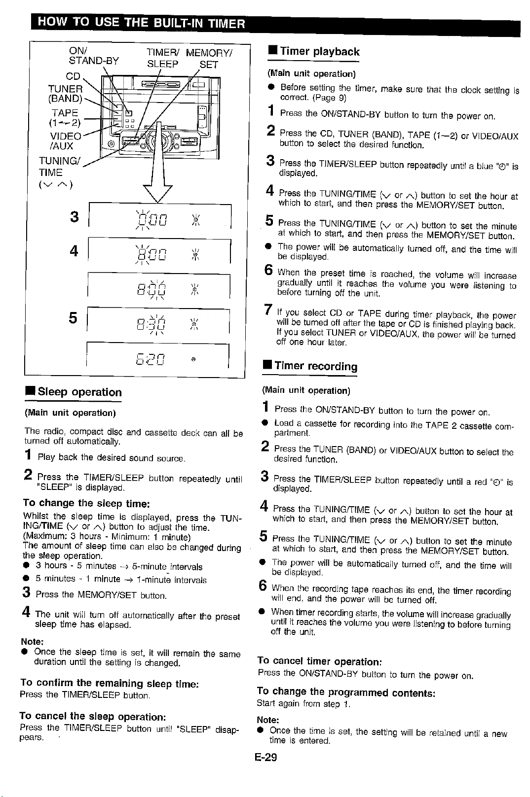
CD-C451H
– 34 –
A
B
C
D
E
F
G
H
1
23456
Figure 34 SCHEMATIC DIAGRAM (13/14)
• NOTES ON SCHEMATIC DIAGRAM can be found on page 18.
1234
5
6
7
8
9
10 11 12 13
14
15
16
48 47 46 45 44 43 42 41 40 39 38 37 36 35 34 33
17
18
19
20
21
22
23
24
25
26
27
28
29
30
31
32
64
63
62
61
60
59
58
57
56
55
54
53
52
51
50
49
C534
0.1 (ML)
C535 10/50
C356 10/50
C537 10/50
C538 10/50
C539
220/16
C547
0.022
R530
3.3K
R529
330
R531
3.3K
C540 10/50
C542
220/16
C544
220/16
R511
1K
R510
18K
D516
RL104AT
D515
RL104AT
R512
6.8K
R509
6.8K
R412
330
C531 2.2/50
C532
220/16
R503
1K
R504
1M
C541 220/16
C514 0.082 (ML)
C515 0.0033 (ML)
C517 0.082 (ML)
C519 0.47/50
C521 0.33/50
C523 10/50
C524 10/50
C527 10/50
R507
1K
R506
4.7K
R505
4.7K
C501
0.1 (ML)
C509
0.1 (ML)
C502 1/50
C503 1/50
C504 47/16
C505 0.47/50
C506 0.022
C507 0.047
C508 680P
C545
220P
C550
220P
C549
220P
R518
1K
R519
1K
R501
100K
R502
100K
C543
0.1 (ML)
C533 0.47/50
C530 4.7/50
C529 4.7/50
C528 4.7/50
C526 0.15/50
C525 3.3/50
C510 0.47/50
C512 4.7/50
C511 0.47/50
C513 4.7/50
C516 0.15/50
C518 3.3/50
C520 0.15/50
C522 0.15/50
R508 39K
C548
0.022
X501
8MHz
K
O
L
C
D
B
X
Z
A
W
M
N
E
H
G
F
J
I
Y
L-BPF3
L-BPF1
RT-IN
LT-IN
DC-OUT
C-MODE
GND
NS-BPF1
NS-BPF2
OSC
CLK
DATA
ENABLE
DATA
CLK
VSS
L-BPF2
OSC
OSC
VDD
A/D
NS
D/A
DC-OUT
DC-OUT
L-OUT
R-OUT
S-OUT
D-GND
DET
VCC
IREF
R-BPF3
R-BPF2
R-BPF1
S-DC-OUT
C-DC-OUT
R-DC-OUT
L-DC-OUT
VREF
VCC
C-OUT
S-OUT
R-OUT
L-OUT
AC-GND
L-IN
R-IN
S-IN
DC-OUT3
R-RECT
DC-OUT4
L-RECT
VLR-TH
VLR-1
VLR-2
VCS-2
VCS-1
VCS-TH
L+R-RECT
DC-OUT2
L-R-RECT
DC-OUT1
IC501
LV1035M
DOLBY PRO LOGIC
DECORDER
+B
+B
+BA-12V
A-GND
+B
+B
REC-R-CH
REC-L-CH
REC-R-CH
REC-L-CH
MAIN PWB-A1(3/3)
A-12V
D_5V
RRIN
CIN
CLK
DATA
ENEBLE
RTIN
LTIN
QS_BYP_AR
QS_MO
QS_AC
TO MAIN SECTION(1/3)
P27 12-D
TO MAIN SECTION(2/3)
P32 1-D/E/F
TO MAIN SECTION(1/3)
P27 12-D
TO MAIN SECTION(2/3)
P33 12-D
5.84V
5.82V
5.84V
5.84V
5.84V
0V
0V
0V
0V
5.2V
5.2V
5.86V
5.86V
5.86V
5.86V
5.86V
5.86V
5.86V
5.86V
5.86V
5.86V
5.86V
5.86V
5.86V
5.86V
5.86V
5.86V
5.86V
5.86V
5.86V
5.86V
5.86V
5.86V
5.86V
5.86V
5.86V
5.86V
5.86V
5.86V
5.86V
11.69V
4.13V
3.5V
3.5V
R407
1K
D401
1SS133
R406 1K
R402 1K
R403 1K
R401 1K
C407
0.022
(ML)
C408
0.022
(ML)
C415
0.022
C416
0.022
C425
0.001(ML)
C427
0.082
(ML)
C432
0.0027
(ML)
C430
0.022
(ML)
IC401
QS7777PF
Q-SOUND
C434
0.022
C433
100/16
R408
47K
R410
47K
R409
47K
C409
0.022
(ML)
C418
0.022
C411
0.0047
C417
0.022
C412
0.0047
C410
0.022
(ML)
C426
0.012
(ML)
R404 1K
R405 1K
C405
0.47/50
C406
0.47/50
C413
0.47/50
C420
4.7/50
C419
4.7/50
C421
4.7/50
C423
4.7/50
C414
0.47/50
C431
0.22/50
C429
10/50
C428
10/50
1
1
2
3
4
5
6
7
8
9
10
11
12
131415161718192021222324
25
25
26
27
28
29
30
31
32
33
34
35
36
36
37 38 39 40 41 42 43 44 45 46 47 48
C435
47/
C436
0.022
QXAC3
QXAC4
QXAC2
QXAC1
QXAC5
QXBC1
QXBC2
QXBC3
QXBC4
QXBC5
VCC
QXCC1
QXCC2
QXCC3
QXCC4
QXDC1
QXDC2
QXDC3
QXDC4
FLIN
FRIN
CIN
SUBIN
RLIN
RRIN
MSC4
MSC5
MSC6
VROUT
VRIN
MSC3
MSC2
MSC1
GND
PSAVE(STRB)
MUTE(SCL)
SPREAD(SDA)
AC
AR
MO
BYP
P/S
VDD
RROUT
RLOUT
COUT
FROUT
FLOUT
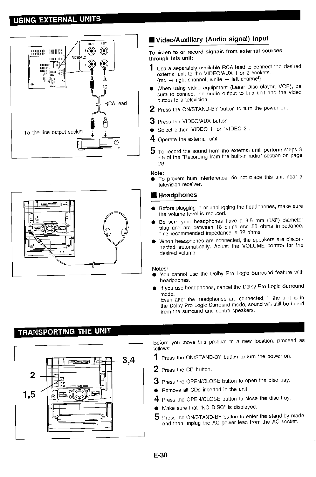
– 35 –
CD-C451H
Figure 35 SCHEMATIC DIAGRAM (14/14)
0V
3.1V
4.8V
4.8V
4.8V
0V
5.0V
0V
4.7V
0V
4.75V
0V
4.85V
–28.4V
–28.4V
–28.4V
–28.4V
–28.4V
–28.4V
–28.4V
4.85V
3.3V
0V
4.8V
4.8V
4.8V
4.8V
4.8V
4.8V
4.9V
4.8V
0V
4.8V
0V
2.3V
2.1V
0V
0V
0V
0V
9
8
7
6
5
4
3
2
1
30
29
28
27
26
25
24
23
22
21
20
19
18
17
16
15
14
13
12
11
10
40
39
38
37
36
35
34
33
32
31
PIN
NO. NO.
VOLTAGE
IC701
PIN
VOLTAGE
4.8V
0V
4.9V
0V
0V
–22.2V
–15.9V
–25.1V
–31.3V
–31.3V
–18.9V
0V
4.7V
0V
0V
0V
0V
4.9V
4.9V
–22V
–28.2V
–31.3V
–22.2V
–18.9V
50
49
48
47
46
45
44
43
42
41
51
64
63
62
61
60
59
58
57
56
55
54
53
52
–28.4V
–28.4V
–28.4V
–28.4V
–22.1V
–31.3V
–13.0V
–31.3V
–28.2V
–31.3V
–19.0V
–31.3V
–31.4V
–31.3V
–31.3V
–31.3V
68
67
66
65
69
80
79
78
77
76
75
74
73
72
71
70
0V
0V
5.2V
5.2V
0V
0V
4.8V
0V
4.8V
0V
0V
4.9V
4.9V
0V
0V
4.9V
0V
4.9V
0V
4.9V
4.9V
0V
0V
3.5V
0V
0V
0V
0V
0V
4.9V
4.9V
5.2V
0V
0V
2.3V
2.3V
4.9V
4.9V
4.9V
4.9V
9
8
7
6
5
4
3
2
1
30
29
28
27
26
25
24
23
22
21
20
19
18
17
16
15
14
13
12
11
10
40
39
38
37
36
35
34
33
32
31
PIN
NO. NO.
VOLTAGE
IC201
PIN
VOLTAGE
4.9V
4.9V
5.4V
4.9V
4.9V
4.9V
4.9V
0V
0V
0V
5.2V
4.9V
4.8V
0V
0V
12.3V
12.3V
4.9V
0V
4.9V
0V
0V
4.9V
4.9V
50
49
48
47
46
45
44
43
42
41
51
64
63
62
61
60
59
58
57
56
55
54
53
52
4.9V
0V
0V
0V
4.9V
0V
4.9V
4.9V
5.2V
5.2V
4.8V
4.9V
0V
0V
0V
0V
68
67
66
65
69
80
79
78
77
76
75
74
73
72
71
70
5.86V
5.86V
5.86V
5.86V
5.86V
5.87V
5.20V
0V
3.50V
4.13V
5.20V
0V
0V
5.84V
5.84V
5.82V
5.84V
5.84V
0V
3.50V
5.20V
5.86V
5.86V
5.86V
9
8
7
6
5
4
3
2
1
24
23
22
21
20
19
18
17
16
15
14
13
12
11
10
PIN
NO. NO.
VOLTAGE
IC401
PIN
VOLTAGE
5.86V
5.86V
5.86V
5.86V
5.86V
5.86V
5.74V
5.86V
5.73V
5.86V
5.86V
5.86V
11.69V
5.86V
5.86V
5.86V
5.86V
5.86V
5.86V
5.86V
5.86V
5.86V
5.86V
5.86V
34
33
32
31
30
29
28
27
26
25
35
48
47
46
45
44
43
42
41
40
39
38
37
36
4.7V
4.7V
4.7V
0V
4.8V
4.7V
4.7V
4.7V
4.7V
–0.1V
0.6V
0V
4.7V
4.7V
4.7V
4.7V
4.7V
4.7V
4.7V
4.7V
4.7V
5.4V
4.8V
5.4V
3.4V
3.5V
4.6V
4.7V
4.7V
4.7V
4.7V
9.4V
4.7V
4.7V
9.4V
2.5V
4.7V
4.7V
4.7V
4.7V
4.7V
4.7V
5V
2.3V
–0.1V
4V
–0.1V
3.6V
–0.1V
4V
0V
4.7V
4.7V
4.7V
4.7V
4.7V
5.4V
4.7V
5.4V
4.6V
4.6V
3.7V
4.7V
4.7V
9
8
7
6
5
4
3
2
1
30
29
28
27
26
25
24
23
22
21
20
19
18
17
16
15
14
13
12
11
10
50
49
48
47
46
45
44
43
42
41
40
39
38
37
36
35
34
33
32
31
PIN
NO.
VOLTAGE
51
64
63
62
61
60
59
58
57
56
55
54
53
52
IC501
0V
2.5V
2.5V
2.5V
4.7V
4.7V
0V
2.5V
2V
0V
0V
0V
2V
2V
2.5V
2.5V
2.5V
0V
2.5V
0V
2V
2.5V
0V
0.7V
2V
2V
0V
0V
0V
1.8V
1.8V
2.5V
2.5V
0V
0V
0V
9
8
7
6
5
4
3
2
1
30
29
28
27
26
25
24
23
22
21
20
19
18
17
16
15
14
13
12
11
10
36
35
34
33
32
31
PIN
NO.
VOLTAGE
IC3
5.1V
0V
2.2V
5.1V
2.2V
2.2V
5.0V
2.9V(3.6V)
5.1V
3.5V(0.3V)
3.9V(1.9V)
3.9V(1.2V)
9
8
7
6
5
4
3
2
1
12
11
10
1.4V
4.0V
1.4V
2.2V
2.4V(0V)
2.4V(0.9V)
0V(1.9V)
0.9V(0.9V)
17
16
15
14
13
20
19
18
2.5V(2.1V)
2.5V(2.1V)
5.1V(5.1V)
3.6V(3.6V)
21
24
23
22
PIN
NO.
VOLTAGE
IC303
0V(0V)
2.6V(0V)
2.6V(0.2V)
2.6V(0V)
5.2V(0V)
0V(0V)
2.6V(0V)
0V(0V)
0V
0V
0V
2.6V(0V)
9
8
7
6
5
4
3
2
1
12
11
10
0V(0V)
2.7V(0V)
5.2V(0V)
0V
0V
0V
0V(0.6V)
0V(5V)
17
16
15
14
13
20
19
18
4.8V(4.8V)
0V(0V)
0V(0V)
0V(0V)
21
24
23
22
PIN
NO.
VOLTAGE
ICT21
0V
35.4V
–35.4V
–35.4V
0V
0V
0V
–33V
33.6V
–0.1V
9
8
7
6
5
4
3
2
1
12
11
10
–0.1V
–0.1V
–32V
–0.1V
0V
15
14
13
PIN
NO.
VOLTAGE
IC901
0.3V(12.3V)
4.8V
2.6V
0V
0V
0V
0.5V(5V)
12V(0V)
0.4V(0V)
4V(0V)
5.1V(5.1V)
0V
9
8
7
6
5
4
3
2
1
12
11
10
0V(2.5V)
0V
0V
2.5V(0V)
5.1V
0.9V
0.9V
1.9V(1.1V)
17
16
15
14
13
20
19
18
0V
2.6V
21
22
PIN
NO.
VOLTAGE
IC302
( ):AM
OTHER:FM(ST)
1.8V
0V
0V
1.0V
1.0V
1.0V
1.8V
1.8V
10.6V
9.1V
1.8V
9.1V
9
8
7
6
5
4
3
2
1
12
11
10
9.3V
1.8V
9.4V
10.8V
0V
4.8V
17
16
15
14
13
18
PIN
NO.
VOLTAGE
IC702
6.5V
6.5V
0V
6.4V
1V
0V
6.5V
2.9V
0V
9
8
7
6
5
4
3
2
1
PIN
NO.
VOLTAGE
IC81
0V
0V
0V
0V
0V
–11.7V
0V
6.4V
8
7
6
5
4
3
2
1
PIN
NO.
VOLTAGE
IC561
0V
0V
0V
0V
0V
–13.2V
0V
11.0V
8
7
6
5
4
3
2
1
PIN
NO.
VOLTAGE
IC651
5.6V
5.5V
5.6V
5.6V
5.6V
0V
5.6V
11.1V
8
7
6
5
4
3
2
1
PIN
NO.
VOLTAGE
IC681
0V
0V
0V
0V
0V
–11.7V
0V
6.4V
8
7
6
5
4
3
2
1
PIN
NO.
VOLTAGE
IC562
0V
0V
0V
0V
0V
–11.7V
0V
6.4V
8
7
6
5
4
3
2
1
PIN
NO.
VOLTAGE
IC563
0V
2.2V
4.8V
4.8V
4.5V
2V
0V
4.8V
0V
2.5V
0V
4.8V
0V
4.8V
0V
0V
2.5V
2.5V
0V
4.8V
1.9V
0V
2.4V
2.5V
0V
4V
4V
0V
0V
0V
0V
0V
0V
0V
4.8V
0V
0V
0V
0V
0V
0V
4.8V
2.5V
0V
0V
0V
4.8V
4.5V
2V
0V
0V
2.1V
0V
2.2V
0V
2.4V
0V
2.4V
0V
0V
0V
4V
0V
0V
9
8
7
6
5
4
3
2
1
30
29
28
27
26
25
24
23
22
21
20
19
18
17
16
15
14
13
12
11
10
50
49
48
47
46
45
44
43
42
41
40
39
38
37
36
35
34
33
32
31
PIN
NO.
VOLTAGE
51
64
63
62
61
60
59
58
57
56
55
54
53
52
IC2
5V
4.8V
5V
4.9V
4.8V
5V
5V
4V
5V
5V
5V
5V
5V
5V
4.9V
5V
4.8V
4.8V
4.8V
4.9V
5V
5V
5V
5V
5V
5V
10V
5V
5V
4.9V
4.8V
5V
4.8V
4.9V
4.9V
5V
–0.1V
–0.1V
0V
5V
5V
4.9V
5V
5V
4.9V
5V
4.8V
4.9V
5V
4.8V
4.9V
4.9V
5V
4.9V
5V
5V
5V
5V
5V
5V
5V
5V
5V
4.9V
9
8
7
6
5
4
3
2
1
30
29
28
27
26
25
24
23
22
21
20
19
18
17
16
15
14
13
12
11
10
50
49
48
47
46
45
44
43
42
41
40
39
38
37
36
35
34
33
32
31
PIN
NO.
VOLTAGE
51
64
63
62
61
60
59
58
57
56
55
54
53
52
IC601
0V
0V
0V
0V
0.6V
2.8V
0V(1.3V)
0.6V
2.8V
2.8V
0V
0V
9
8
7
6
5
4
3
2
1
12
11
10
0V
5.8V
3.6V
2.8V
0.6V
0V
0V
0V
17
16
15
14
13
20
19
18
2.8V
0.6V
0V
0V
21
24
23
22
PIN
NO.
VOLTAGE
IC101
2.5V
2.4V
2.5V
2.4V
1.5V
0V
2.5V
2.5V
0V
2.5V
2.4V
2.5V
2.5V
2.5V
2.5V
2.5V
2.4V
2.5V
2.5V
2.5V
2.4V
4.2V
2.2V
1V
1V
2.5V
4.8V
2.4V
2.4V
2.5V
2.5V
2.5V
2.5V
2.5V
2.5V
2.5V
2.5V
2.5V
2.5V
2.5V
2.5V
2.2V
2.2V
0V
0V
4.8V
4.8V
0V
0V
4.8V
0V
0V
2.5V
0V
0V
2.4V
4V
4V
0V
0V
4.8V
2.5V
0V
4.8V
9
8
7
6
5
4
3
2
1
30
29
28
27
26
25
24
23
22
21
20
19
18
17
16
15
14
13
12
11
10
50
49
48
47
46
45
44
43
42
41
40
39
38
37
36
35
34
33
32
31
PIN
NO.
VOLTAGE
51
64
63
62
61
60
59
58
57
56
55
54
53
52
IC1
( ):CD NORMAL REC
OTHER:CD NORMAL PLAY
7
8 9 10 11 12
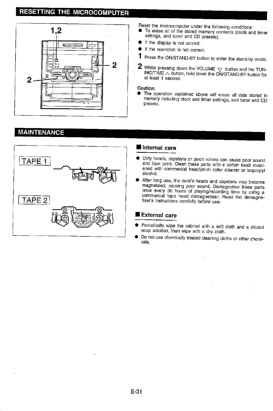
CD-C451H
– 36 –
A
B
C
D
E
F
G
H
1
23456
Figure 36 WIRING SIDE OF P.W.BOARD (1/8)
R167
R166
R115
R114
R113
R106
R104
R192
C106
R108
C108
RM16
RM19
RM20
RM08
RM07
R147
C155
C101
R107
R162
RM05
RM11
RM06
RM12
R578
R243
R242
R234
R235
R240
R253
R276
R254
R274
R272
R255
R256
R257
1
5
10
15
20
24
25
30
35
40
41
45
50
55
60
64
65
70
75
80
R258
C552
C558
R557
R563
R569
R556
R568
C557
C551
R562
R571
R564
R570
R565
R552
C569
C554
C560
R559
R558
C559
C553
R572
C69
8
R683
R689
C570
R554
C563
R567
C561
R566
R573
C556
C555
R560
R264
R203
R238
R232
R228
R229
R230
R244
R222
R221
R671
C695
R266
R675
C
R672
R682
C
R680
R674
R686
C694
R695
R692
R691
C689
R687
C685
C686
C690
R688
R690
R681
R685
R619
R617
R615
R613
R611
C207
C204
C206
R265
R141
C139
R134
R145
C140
C1
R135
C129
R142
R140
R146
R136
R154
R153
C144 C130
R126
R132
R101
C102
C114
C112
C113
R139
C143
C127
R219
R280
R218
R220
R205
R206
R207
R208
R210
R209
R211
R212
C107
C105
R103
R105
R122
C120
R124
R117
C111
C203
C205
R121
C119
R123
R125
R131
R143
IC201
R168
R120
L104
C150
Q111
C152
C162
R193
C109
Q109
Q110
C163
L103
R160
Q124
Q129
Q130
R170
R171
C156
C161
RM10
QM03
C151
Q128
Q126
R164
DM02
CM01
QM02
QM05
R277
R263
R262
R261
R260
R259
R247
R246
R245
LUG1
L201
DZ551
R241
D551
C564
D552
R576
D553
C565
R577
R551
D555
R579
D557
D558
C201
D554
C566
D201
R279
R237
C250
C251
C252
R227
R225
R224
R226
C568
D556
R580
C567
R553
IC563
IC562
R555
C562
R575
C202
R233
BI201
R202
R271
DM03
RM15
RM14
RM09
R110
R109
CNP101
12
CNS101
TO TAPE
MECHANISM
P38 1-E
P38 2-F
TO HEAD PWB
FWM1
1
13
CNS102
TO TUNER PW
B
P43 8-C
CNP303
CNS11
3
1234567
C133
C128
C121
C117
L107
C115
R119
R102
Q107
Q108
R111
C122
L108
C116
R191
R118
R112
Q106
C118
Q105
Q103
Q104
L102
C147
C134
Q118
R138
C142
Q121
Q122
C136
C145
C146
R158
C110
C605
C607
R215
R214
R213
BI601
6
121110987654
1
C141
R137
1
510
12
BCE
13152024
L101
C135
Q117
C683
C210
C682
R216
R217
1
3
5
7
9
11
13
15
17
19
21
23
2
4
6
8
10
12
14
16
18
20
22
24
114
1
2
3
4
5
1
2
3
4
5
5
RD
WH
GY
WH
GY
WH
6
7
8
9
10
11
12
13
14
RD
BL
BL
BL
BL
BL
BL
BL
BL
BL
BL
BL
BL
BL
E
1
2
3
4
5
6
7
8
9
10
11
12
13
C
B
B
C
E
B
C
E
B
C
E
B
C
E
B
C
E
B
C
E
B
C
E
E
C
B
E
C
B
E
C
B
E
C
B
E
C
B
E
C
B
E
C
B
BCE
BCE
123
123
3
2
1
C681
C609
D609
D605
D604
D608
R696
R684
C687
D209
D210
R694
R693
R574
R561
C684
C693
C688
C691
C692
C680
Q671
Q
Q674
C604
C603
D
C615
C611
C601
R156
R155
E
321
ECB
ECB
C
B
WTM1
IC561
XL201
CNP701
IC101
CNP102
CNS303
IC681
CNS803
8
7
6
5
4
3
2
1
8
7
6
5
4
3
2
1
8
7
6
5
4
3
2
1
8
7
6
5
4
3
2
1
24
CNS12
1
P42 6-B
CNP701
P39 11-G
TO DISPLAY PWB
TO CD SERVO PWB
CNP12
P38 3-A
TO TAPE MECHANISM PWB
CNPM1
TO TAPE
MECHANISM
FLAT CABLE(263)
P39 9-G
TO CD SERVO PWB
CNP11
R249
R250
R251
C429
C431
C423
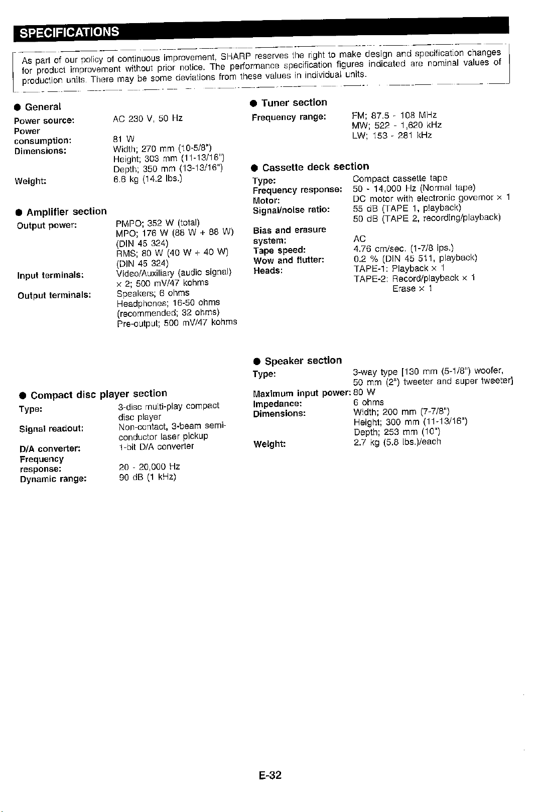
– 37 –
CD-C451H
Figure 37 WIRING SIDE OF P.W.BOARD (2/8)
7
8 9 10 11 12
BR
COLOR TABLE
RD(R)
OR
YL
GR
BL
VL
GY
WH(W)
BK
PK
BROWN
RED
ORANGE
YELLOW
GREEN
BLUE
VIOLET
GRAY
WHITE
BLACK
PINK
C698
R671
C695
R266
R675
C696
R672
6
82
C697
R680
R674
R686
R
681
R
685
R619
R617
R615
R613
R611
R135
C129
R144
C672
R652
R604
R602
R606
R620
C614
C677
R621
C613
R661
R252
R614
R618
R641
R678
C657
R649
R697
R624
R663
R677
C679
C661
C678
C662
R662
R626
R634
C658
R635
R631
R627
C655
R633
R630
R632
C656
R648
12345678
R645
C663
R644
R623
R622
C664
R505
R509
R506
R512
R511
R657
C673
R653
R656
R651
C671
R655
R654
C670
R650
C674
R531
SHASSIS
GND
R529
R530
R510
R508
R504
1
5
10
15
1617
20
25
30
32
33 35
40
45
48 49
50
55
60
64
R503
R501
R502
IC601
1
5
10
15 16
17
20
25
30
3233
35
40
45
48
49
50
55
60
64
IC501
D606
TO TUNER PWB
P43 8-C
CNP303
P40 2-D
TO POWER PWB
CNP803
L102
8
C110
C605
C607
110987654321
1
C683
C210
C
682
C681
C609
D605
C684
Q201
Q671
Q673
R699
Q674
D205
D204
D207
D206
D203
D202
R679
C699
Q672
D208
Q609
D611
D610
C633
C629
C625
C641
C637
C631
C627
C623
R625
C643
C635
C639
C618
C616
C612
R610
R608
C606
C602
C604
C603
D601
R669
C617
C615
C611
C601
C676
C624
C608
C610
R612
R156
R155
C199
C502
C506
C505
C503
R519
R518
C523
C507
C508
C549
C550
C545
C541
C514
C515
C517
C521
C519
C648
C632
C665
C628
C626
C630
C634
C636
Q601
Q602
C668
C669
C645
R659
R637
R629
R636
R628
C649
R660
C640
C666
C644
C638
C642
C646
R616
C647
C667
Q603
Q676
E
C
B
E
C
B
E
C
B
E
C
B
E
C
B
E
3
2019181716151413121110987654321
21
ECB
ECB
ECB
C
B
Q604
R642
R698
C651
R646
R676
R647
R673
Q675
C209
DZ201
C208
1
2
3
4
5
6
7
8
R639
C660
C652
R638
C659
MAIN PWB-A1
JK452
R658
R507
C524
C527
D607
C539
C544
C542
C531
C532
D516
C540
D515
C538
C548
C504
C530
C533
C535
C537
D540
D541
C547
C536
C534
C543
C529
C528
C525
C526
C522
C520
C518
C516
C511
C513
C512
C510
C509
C501
C
NS303
CNS803
X501
L-CH
VIDEO/AUX 2
R-CH
SURROUND
JK452
CENTER
L-CH
VIDEO/AUX 1
R-CH
IC651
B
C
E
B
C
E
IC401
C414 C435
C413
C417
C415
C436
C410
C411
C409
C434
R401
D401
C412
C408
R406
R407
R405
R404
C432
C430
C428
C426
C420
C418
1
5
10
12
13
24
37
15
20
25
30
35
40
45
48
C421
C425
C427
C429
C431
C423
C406
C407
R408
C433
R410
R403
R402
R409
C405
C419
C416
R412
C473
C471
R475
C475
R471
R473
C472
R474
C474
R472
R487
C481
R489
C482
R478
C478
C477
C484
C483
C485
R477
C480
C476
R476
IC471
R481
C488
R483
C490
C479
R482
R484
R601
R603
R666
R665
C621
C619
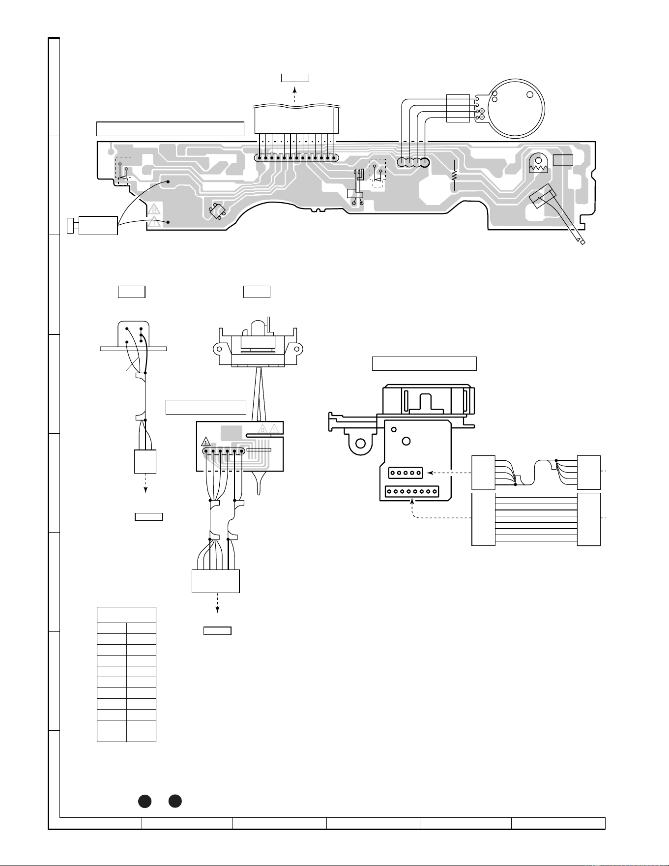
CD-C451H
– 38 –
Figure 38 WIRING SIDE OF P.W.BOARD (3/8)
A
B
C
D
E
F
G
H
1
23456
CNPM2
SWM5
F. A. S
SWM4
REC RVS
SWM3
REC FWD
VRM1
TAPE
SPEED
1
FWM2
4
RM1
3
4
2
1
PHM1
SWM6
CAM
CNS1B
CNS1A
CNS2B CNS2A
BL
YL
PK
WH
BK
GY
RD
WH
GY
WH
GY
WH
GY
WH
BL
PK
WH
YL
BK
1
2
3
4
5
6
7
8
1
2
3
4
5
6
7
8
1
2
3
4
5
1
2
3
4
5
PICKUP UNIT(306)
TAPE MECHANISM PWB-F
HEAD PWB-G
WH
PK
BK
TAPE 1
PLAYBACK HEAD(254-8)
TAPE 2
RECORD/PLAYBACK/ERACE HEAD(254-9)
GY
GY
GY
WH
CNS102
CNS101
YL
BK
BL
PK
WH
BK
7654321
2
1
3
6
BI 102
1
WH
BK
PK
CNP102
TO MAIN PWB
P36 1-G
TO MAIN PWB
P36 1-F
CNP101
TAPE MOTOR
MM1
WTM1
TO MAIN PWB
P36 1-E
H
L
SOLENOID
SOLM1
WH
YL
BL
PK
WH
BK
FLAXIBLE PWB
CNPM1
113
1
13
FWM1
BR
COLOR TABLE
RD(R)
OR
YL
GR
BL
VL
GY
WH(W)
BK
PK
BROWN
RED
ORANGE
YELLOW
GREEN
BLUE
VIOLET
GRAY
WHITE
BLACK
PINK
• The numbers 1 to 12 are waveform numbers shown in page 44.
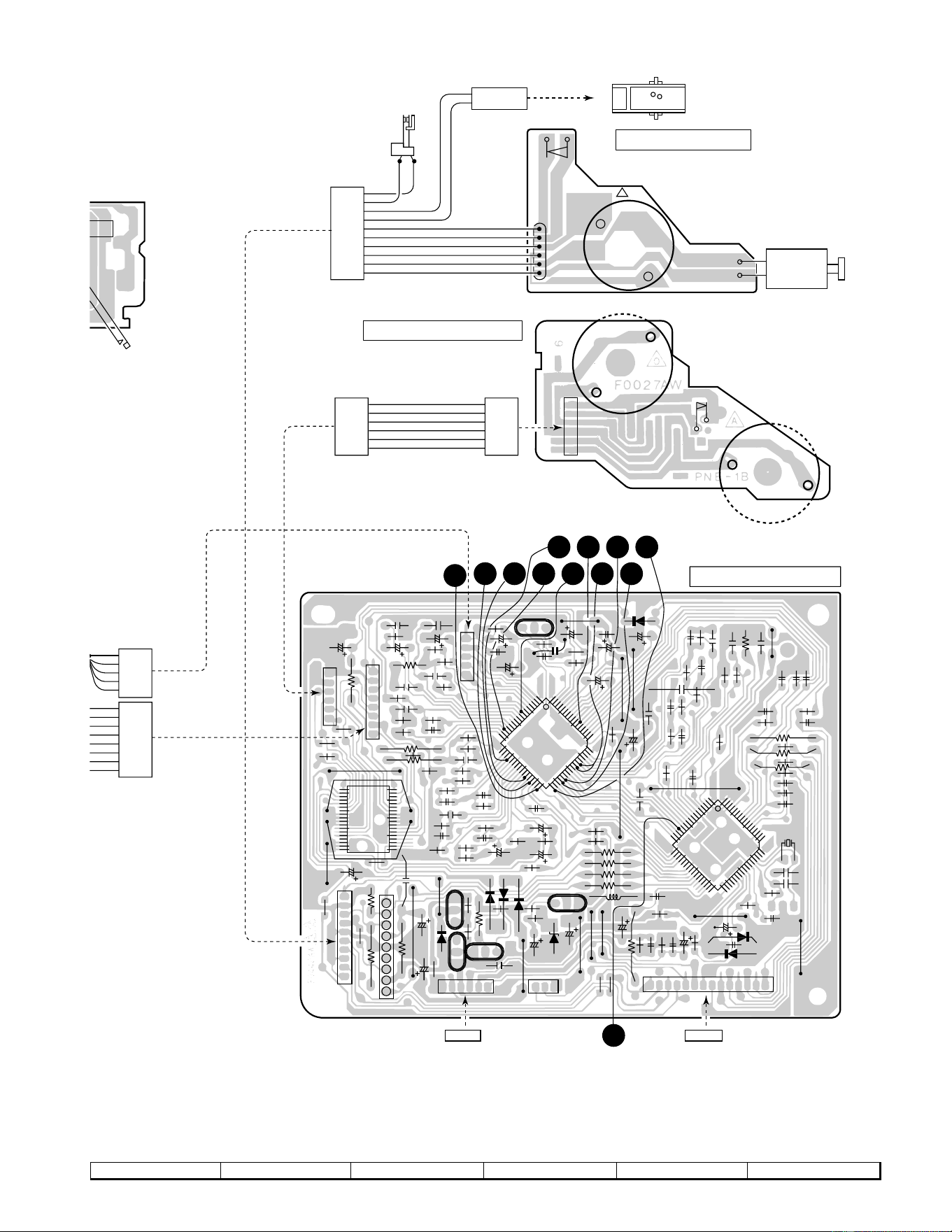
– 39 –
CD-C451H
Figure 39 WIRING SIDE OF P.W.BOARD (4/8)
7
8 9 10 11 12
+
-
+
-
PICK UP IN
SLED MOTOR
DISC MOTOR
M2
CNP3A
SW4
M1
+
-
1
2
3
4
5
6
C
NPM2
SWM5
F. A. S
TAPE
S
PEED
CNS5
2
1
2
1
CNS10
WH
RD
GY
WH
BR
WH
GY
OR
WH
GY
10
1
BIM5
6
9
8
7
6
5
4
3
2
1
SW2
MECHA UP
SW1
OPEN/CLOSE
M3
T/T UP/DOWN LOADING
SW3
DISC NUMBER
CNS1A
CNS2A
CNS3BCNS3A
BL
YL
PK
WH
BK
RD
WH
GY
WH
GY
WH
1
2
3
4
5
6
7
8
1
2
3
4
5
6
1
2
3
4
5
6
1
2
3
4
5
CD MOTOR PWB-D
SENSOR PWB-E
SOLM2
SOLENOID
CD SERVO PWB-C
CNP3
R37
CNP2
C35
R13
C7
R12
C8
R11
C6
R14
R15
C9
R10
C5
R9
R8
C4
C54
CNP1
1
5
10
15
20
25
30
35
40
45
50
55
60
5
10
15
20
25
30
35
40
45
50
55
60
64
C15
R2
C1
C3
Q1
R1
C2
C33
R46
C31
C85
C34
C32
R43
R40
R38
C30
R42
C23
R52
R53
C48
C47
C38
C27
R41
C26
C40
R51
C39
D1
C28
C84
C25
C57
C46
R47
R60
C37
XL1
IC2
C45
C49
C44
R57
R58
R62
R59
R61
R63
R50
C22
R45
C29
C24
C56
R44
IC1
17
1
2
3
4
5
6
7
8
1
2
3
4
5
6
1
2
3
4
5
16
49
48
33
32
1
64
17
16
49
48
33
32
R35
R36
C21
C20
R32
R88
R89
C19
36
1
5
10
15
1819
20
25
30
35
C36
R82
R16
R48
R19
R20
R21
C10
R17
R18
C11
R23
R24
C13
R26
R29
R33
R81
C18
C17
C12
C14
R25
R22
IC3
R27
C16
R28
C81
D91
R83
C82
IC81
R85
CNP10
CNP11
CNP99
123321456
1
2
3
4
5
6
7
8
9
1
2
3
4
5
6
7
8
9
10
R86
R80
Q93
Q91
R87
D3
D2
D4
ZD61
C51
C52
C71
R34
C75
R66
R64
Q52
R90
R91
L61
CNP12
CNS12
TO MAIN PWB
P36 1-D
CNS11
TO MAIN PWB
P36 1-G
1413121110987654321
R93
R71
R73
R54
C73
R74
C74
C72
R72
C50
C43
R55
C83
C53
D81
D82
R31
R30
1
2
3
BCE
Q51
123
B
C
E
BCE
C41
C42
11
5398
6421
1012
7

CD-C451H
– 40 –
Figure 40 WIRING SIDE OF P.W.BOARD (5/8)
A
B
C
D
E
F
G
H
1
23456
POWER PWB-B
CNS803
TO
MAIN PWB
P37 7-A
Q801
C811
ZD822
ZD820
D822
D823
C828
C804
C812
C813
C829
C806
C805
D804
D805
D803
D806
R802
R803
R801
ZD801
C802
C803
D809
D808
D807
R827
R828
D824
R806
R805
ZD802
R838
C827
C825
C831
C823
R837
C824
R836
C826
R835
Q825
R826
R829
R824
C820
Q824
R807
R963
D827
C817
C808 C807
F805
1.6A 250V
F831
T500mA L 250V
F803
T3.15A L 250V
F802
T3.15A L 250V
D801
CNP802
1
1
2
3
4
5
6
7
8
9
10
11
12
13
14
15
16
17
18
19
20
23456789
Q902
Q903
R907
R922
R918
R905
C915
R965
R964
C904
C907
C911
C912
C917
C918
R913
R912
C909
C910
R932
C903
R901
C901
Q822
Q826
15141312111098765432
R825
R969
B
C
E
B
C
E
B
C
E
B
C
E
E
321
321
ECB
Q827
123
C
B
E
C
B
R820
C902
R902
C905
R904
R903
Q823
CNP803
Q820
1234
SO901
SPEAKER
TERMINAL
CHASSIS
GND
L-CH
R-CH
FRONT
6 OHMS
MIN.
R921
R943
R945
R973
R972
R948
R947
R917
C916
C924
C936
C947
C948
C952
C951
C958
C956
C955
C957
C961
C962
R915
R916
D902
R962
R923
C923
C972
C970
R924
C97
7
IC901
F902
T4A L 250V
F901
T4A L 250V
C937
R937
C
9
C934
CHASSIS
GND
L901
L903
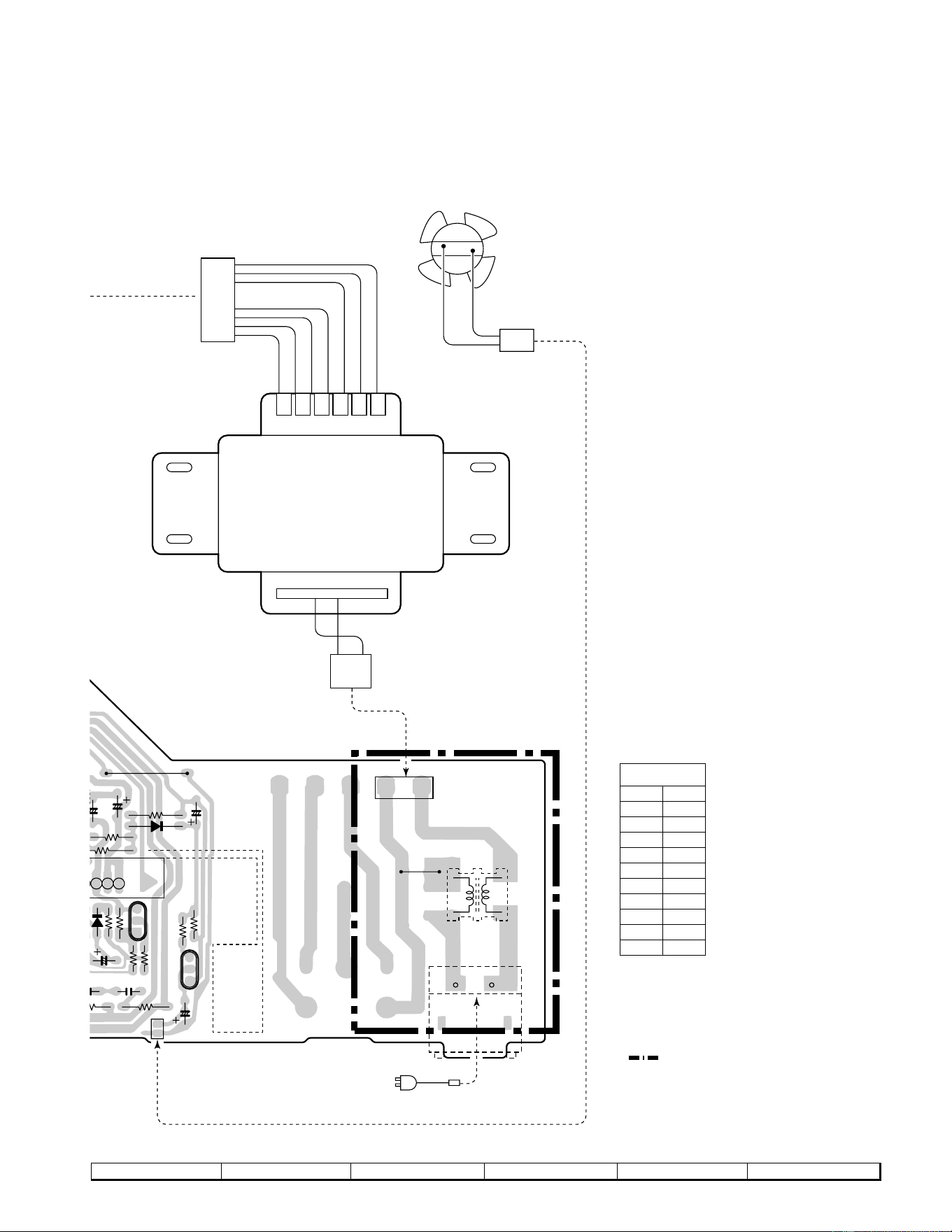
– 41 –
CD-C451H
Figure 41 WIRING SIDE OF P.W.BOARD (6/8)
7
8 9 10 11 12
1
2
3
4
5
6
7
8
9
BR
COLOR TABLE
RD(R)
OR
YL
GR
BL
VL
GY
WH(W)
BK
PK
BROWN
RED
ORANGE
YELLOW
GREEN
BLUE
VIOLET
GRAY
WHITE
BLACK
PINK
BL
CNS801
RD
21
RD
CNS804
BR
2
1
M901
FAN MOTOR
T801
POWER
TRANSFORMER
12
When Serving, pay attention
as the area enclosed by this
line ( ) is directly
connected with AC main
voltage.
AC POWER CORD
AC POWER INPUT
230-240V/50Hz
CNP801
5
R
964
C904
C907
321
Q901
R910
D902
R962
CNP804
2
1
R911
R914
C977
R934
C978
R968
R967
SO801
3
7
C935
3
4
Q905
R966
D903
C979
B
C
E
E
C
B
RD
BL
RD
CNS802
YL
YL
BR
BR
L801
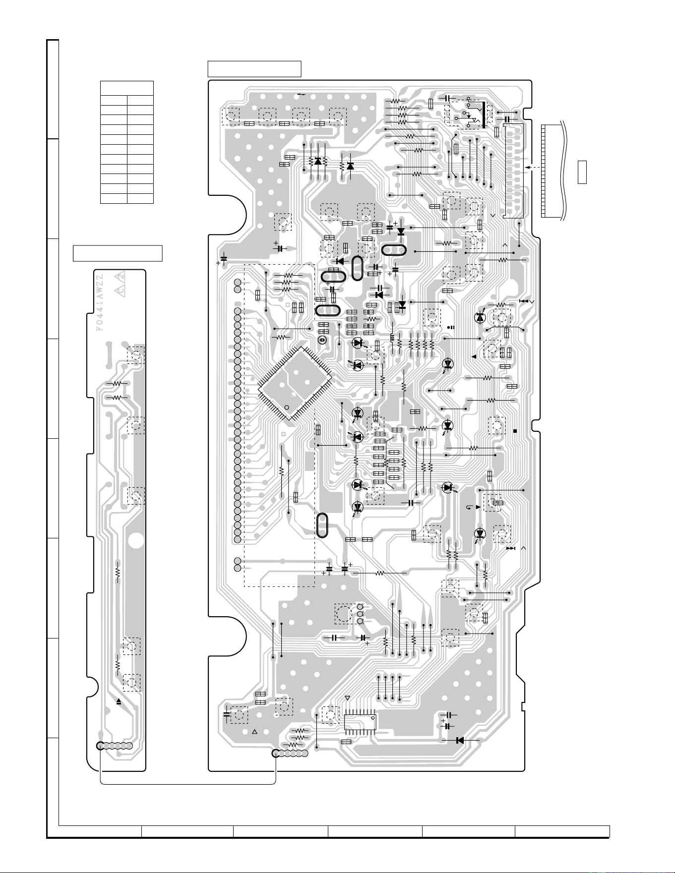
CD-C451H
– 42 –
A
B
C
D
E
F
G
H
1
23456
Figure 42 WIRING SIDE OF P.W.BOARD (7/8)
BR
COLOR TABLE
RD(R)
OR
YL
GR
BL
VL
GY
WH(W)
BK
PK
BROWN
RED
ORANGE
YELLOW
GREEN
BLUE
VIOLET
GRAY
WHITE
BLACK
PINK
R734
RD22
R701
R776
R703
R705
R707
R704
R706
R708
R702
RD29
R777 R735
RD25
RD26
RD35
R709
R710
R711
RD17
RD33
RD31
RD32
RD30
RD34
C723
RD20
RD18
C701
C722
C726
R736
R767
R772
C708
R770
C703
C704
1
5
10
15
20
24
25
30
35
4041
45
50
55
60
64
65
70
75
80
R729
R727
R726
R728
R768
R732
R775
R774
RD21
R765
R771
RD08 RD09 RD10
R731
C721
RD13
RD12
R766
RD14
R763
C706
RD01
RD02
RD28
IC702
IC701
SW709
CD
SW710
TUNER
(BAND)
SW711
TAPE
12
DISPLAY PWB-A2
SWITCH PWB-A3
SW712
VIDEO/AUX
D707
C730
C729
SW733
VOLUME
DOWN
1
5
9
10
15
18
C724
SW725
VOLUME
UP
SW726
X-BASS
FW701-1
FW701-2
1
1
SW708
OPEN/
CLOSE
RD07
SW707
DISC SKIP
RD23
B
C
E
RX701
1
2
3
C710
C715
R773
R744
SW740
BEAT CANCEL
(TAPE 1 EDIT)
SW739
CD/TAPE 1
EDIT
SW736
REVERSE
MODE
R738
R739
SW729
FWD
LED702
R743
Q701
C712
C716
RD15
RD16
R717
R718
LED701
R737
RD24
SW734
EQUALIZER
DEMO
C725
SW718
CENTER MODE
/PHAMTOM
LED711
LED710
SW706
DISC 3
RD06
R778
SW704
DISC 1
SW705
DISC 2
RD05
RD04
XL701
SW719
CENTER MODE
/NORMAL
LED708
LED709
RD19
L701
SW721
DOLBY PRO LOGIC
/BYPASS
LED707
LED706
R719
R715
R714
R713
R712
R733
R716
SW737
REV
R741
R742
SW728
STOP
LED705
LED703
LED704
SW738
REW/
PRESET
DOWN
SW730
FF/
PRESET
UP
R740
RD27
SW724
TUNING UP
/TIME
RD03
SW731
MEMORY
/SET
SW703
TIMER/
SLEEP
SW723
REC
PAUSE
D709
D708
C732
C733
Q710
C709
D705
C731
SW714
PTY./TI
SEARCH
SW715
ASPM
SW716
DISPLAY/MODE
SW713
EON
D706
Q704
Q706
C707
Q705
ECB
ECB
E
1
2
3
CB
SW701
ON/STUND-BY
R722
R721
R720
C713
41
40
37
36
35
34
33
32
31
30
29
28
27
26
25
24
23
22
21
20
19
18
17
16
15
14
13
12
11
10
9
8
7
6
5
2
1
C702
ZD710
R790
R769
ZD701
RD11
SW702
CLOCK
SW732
TUNING
DOWN
/TIME
C734
24
24
1
22
20
18
16
14
12
10
8
6
4
2
23
21
19
17
15
13
11
9
7
5
3
1
C735
JK700
HEAD PHONE
R792
R793
R791
R779
R749
R780
R781
FL701
CNS701
TO MAIN PWB
P36 1-B
CNP701
FLAT CABLE(263)
1
3
4
5
2
R748
R747
R746
R783
RD36
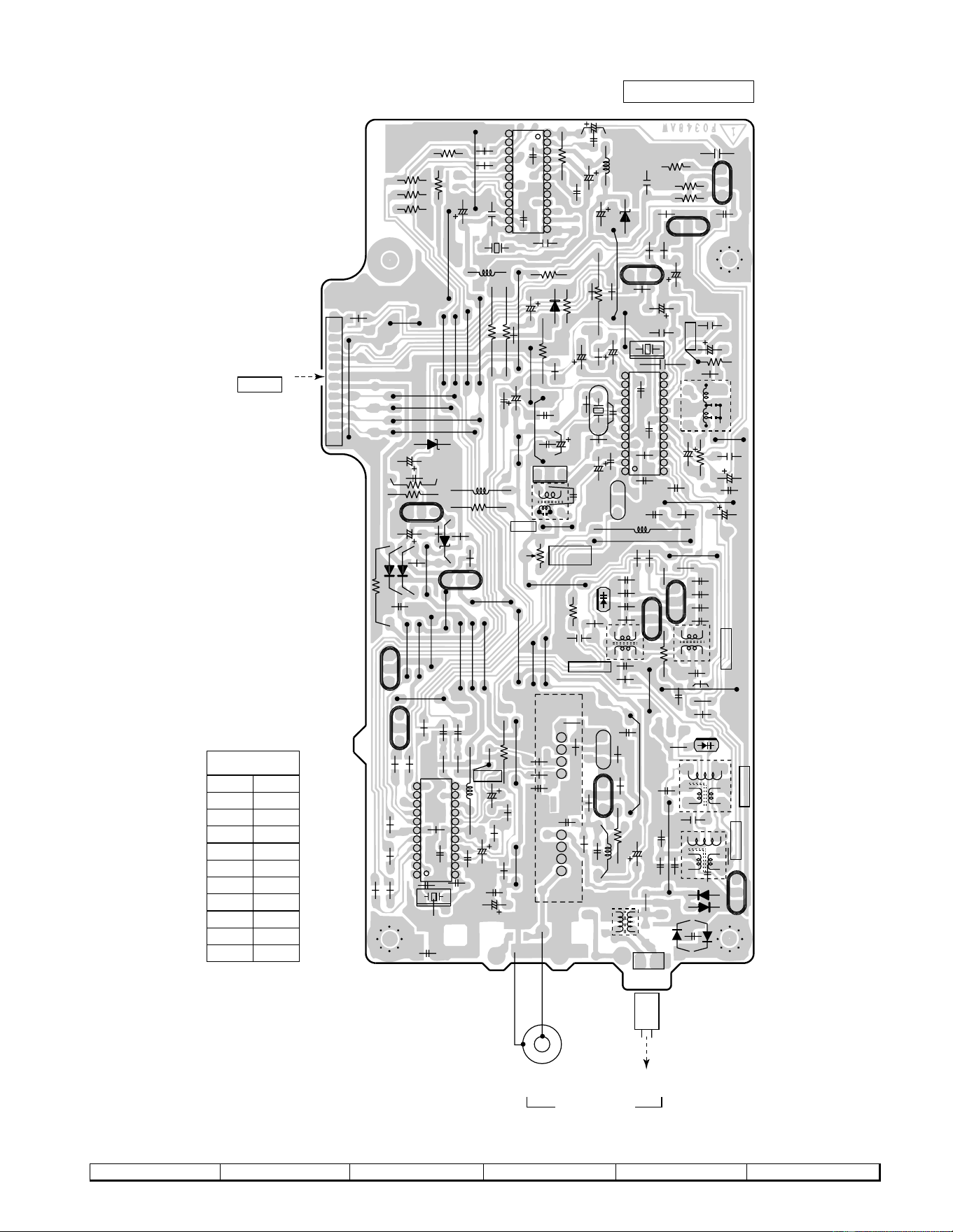
– 43 –
CD-C451H
Figure 43 WIRING SIDE OF P.W.BOARD (8/8)
R362
C341
R348
R347
C330
C333
C321
R349
C339
R346
L342
C346
R369
C347
R344
C345
1
R345
R301
C384
R324
TP301
C329
R337
X352
C382
1
5
10
12
15
20
22
R378
C387
IC302
C394
C397
C381
C301
C337
R335
T305
C324
C326
C327
C325
R333
R332
C332
R319
C336
C335
C334
R323
C328
R331
VD301-1
R334
C331
Q302
C322
T301
C323
D302
D301
D304
D303
R376
R360
R397
Q362
C392
C385
C386
C393
R379
R381
R380
L351
R336
C380
R371
R372
R373
R374
T351
C342
C354
C355
R385
R383
R387
R384
C395
C352
C351
L353
R358
C343
R351
IC303
C366
C350
C353
C361
C363
C362
TP302
C364
C365
R350
C367
C369
X351
R356
R357
C368
C374
R361
C373
C371
R393
R364
R363
R355
R352
CF351
C399
C398
C358
C357
R353
C356
R359
R367
RT49
R354
LT22
12
11
10
9
8
7
6
5
4
3
2
1
RT48
RT37
RT36
RT35
RT28
RT30
CT29
CT22
1
5
10
1213
15
20
24
CT25
CT24
CT37
CHASSIS
GND
R366
R365
R370
RT21
RT29
ICT21
RT26
CT28
CT27
CT26
XT21
R377
D353
R368
C375
CNP303
C370
ZD351
C396
CF352
R392
L352
R391
R395
Q361
ZD352
C391
VR351
D352
D351
R382
Q360
Q371
FE301
CNP301
21
L341
Q301
T302
CF301
T306
Q304
Q303
VD301-2
CF302
L354
Q353
C372
Q354
CT43
ZDT21
RT34
RT33
CT36
QT21
CT21
RT32
LT21
C302
CT23
13
15
20
24
1
10
12
11
C338
2
3
4
5
6
7
8
B
C
E
ECB
ECB
1
2
3
123
123
ECB
B
C
E
3
2
1
E
C
B
E
C
B
3
2
1
E
C
B
B
C
E
CHASSIS
GND
CHASSIS
GND
CNS303
TO MAIN PWB
P36 6-H
TUNER PWB-H
SO301
MW/LW
LOOP
ANTENNA
FM 75 OHMS
BR
COLOR TABLE
RD(R)
OR
YL
GR
BL
VL
GY
WH(W)
BK
PK
BROWN
RED
ORANGE
YELLOW
GREEN
BLUE
VIOLET
GRAY
WHITE
BLACK
PINK
21
AM IF
MW OSC.
LW OSC.
MW ANT.
LW ANT.
FM MUTE
LEVEL
7
8 9 10 11 12
CD-C451H
– 44 –
WAVEFORMS OF CD CIRCUIT
3
5ms
0.50 V
IC1 20 F.E
1
5ms
5.0 V
IC1 54 DRF
STOP PLAY
FOCUS SERCH
1
3
5
4
2
6
7
8
9
10
11
3
4
5
6
7
8
9
6
7
8
10
11
12
9
6
7
8
9
12
0.5ms
1.00 V
HF
0.5ms
5.0 V
HFL
0.5ms
5.0 V
TES
1
2
3
CUE
0.5ms
1.00 V
HF
1
2
3
0.5ms
5.0 V
HFL
0.5ms
5.0 V
TES
REVIEW
50ms
10.0 V
JP+
CUE
50ms
10.0 V
JP-
50ms
0.50 V
JP
50ms
1.00 V
TE
0.5ms
10.0 V
JP+
0.5ms
10.0 V
JP-
0.5ms
0.50 V
JP
0.5ms
1.00 V
TE
REVIEW
50ms
10.0 V
JP+
50ms
10.0 V
JP-
50ms
0.50 V
JP
50ms
1.00 V
TE
0.5ms
10.0 V
JP+
0.5ms
10.0 V
JP-
0.5ms
0.50 V
JP
0.5ms
1.00 V
TE
PLAY
20ms
1.00 V
SPO
NORMAL DISC
TN0=01
20ms
2.00 V
CLV+
PLAY
TCD-712 (140mm)
TN0=01
50ms
1.00 V
SPO
50ms
2.00 V
CLV+
PLAY
TCD-712
5s
100mV
SLD
1
0.5s
100mV
SLD
1
– 45 –
CD-C451H
TROUBLESHOOTING (CD SECTION)
When the CD does not function
When the CD section does not operate When the objective lens of the optical pickup is dirty,this section may not operate.Clean
the objective lens,and check the playback operation.When this section does not operate even after the above step is taken,check
the following items.
Remove the cabinet and follow the troubleshooting instructions.
"Track skipping and/or no TOC(Table Of Contents) may be caused by build up of dust other foreign matter on the laser pickup lens.
Before attempting any adjustment make certain that the lens is clean. If not, clean it as mentioned below."
Turn the power off.
Gently clean the lens with a lens cleaning tissue and a small amount of isopropyl alcohol.
Do not touch the lens with the bare hand.
• When the turntable fails to stop.
Is from 5 V till 0V down pulse (approx. 300 ms) input
Check the SW3 and the wiring from the IC201 pin 54 to the
SW3.
No
No
into the IC201 pin 54 when the turntable is rotating?
5V
2.5V
0V
Yes
Check IC2 pin26 Q91 and Q93 and the periphery.
Check the SW2 MECHA UP SW and the wiring from the
IC201 pin 21 to the SW2 MECHA UP SW.No
Yes
Is there following voltage input on the IC201 pin 54 in the
specific state?
When the CD mechanism is moved up: 0V
In other states: 5V
Yes
Is there following voltage input on the IC201 pin 54 in the
specific state?
In other states: 5V
When the CD mechanism is moved up: 0V
• When turntable fails to move.
Check the SW2 MECHA UP SW and the wiring from the IC201
pin 54 to the SW2 MECHA UP SW.
Is 4V output from the Q91 emitter during operation stated
above?
Yes
Yes
Check the wiring of IC2 pin 26 and Q93 BASE.
OK
No
No
Is L output from the IC2 pin 26 during SEC when the disc skip
switch is pressed?
Yes
Check turntable motor and turntable mechanism.
Check Q91, Q93 and the periphery.
IC701 defective.
IC2 defective.
CD-C451H
– 46 –
• When the CD tray fails to open or close.
Is there following voltage input in specific state of IC701 pin 53?
Open state: 0V
Close state: 0V
Intermediate state between open state and close state: 5V
Is H output to IC2 pin 24 or 25 for 7 seconds when the OPEN/
CLOSE key is pressed?IC81 is defective. Replace it.
Is 4V output between IC81 pins 3 and 7 during operation
stated above?
Check the loading motor (M3) and the loading mechanism.
Yes
Yes
Yes
No
No
IC2 defective.
No
Check the periphery of IC81.
IC81 defective.
OK
OK
Check the OPEN CLOSE SW and the wiring from the IC701
pin 53 to the OPEN CLOSE SW.
Check the wiring of the IC2 pins 24 and 25, IC81 pins 1 and 3.
• The CD function will not work.
The CD operating keys don't work.
Check the CD, DSP, power supply, and 16.93 MHz clock, and
reset terminal.
Check the waveform of SCK, SO (DATA) and SI (COMM).
Yes
Yes
See if the pick-up is in the PICKUP IN SW position.
If the items mentioned above are OK, check the main
microcomputer IC701.
Yes
Yes
No
Yes
No
• The CD operating keys work.
Check the Focus - HF system.
Playback can be performed without a disc.
Focus search OK
Does the pick-up move up and down twice?
Does the output waveform of IC1(16)(FD) match that shown in
Fig. 47?
Check the IC1(50)(CLK) line, 4MHz.
Check the microcomputer data on pins (51)(CL), (52)(DAT)
and (53)CE.
Check the area around IC3-CNP2.
Yes
Yes
Figure 46
Focus search is
performed two
times when play
operation is done
without disc.
0.5s
0.50 V
IC1 16 FD
2
1
0.5s
0.50 V
IC1 7 TE
– 47 –
CD-C451H
• Playback can only be performed when a disc is
loaded.
Is HF waveform normal (see the Fig. 47-1, 2)?
Check the tracking system.
Is the Focus servo active? (Can you hear it working?)
Check the laser diode driver.
Check the area around IC1(16) - (21) (focus servo circuit).
No
Yes
Yes
Yes
Does the DRF signal change from "L" to "H"?
No
Yes
If the disc is not turning, the DRF
should not change to "H".
Level is abnormal.
No
Yes
Waveform is unstable.
Check the spin system.
Yes
Check the periphery of
IC1 pins 41 and 42.
Check the spin system.
Figure 47-2
Figure 47-1
Waveform in case of
normal play-back
HF
1.0V/DIV
0.5µsec/DIV(DC)
(When playing
back the disc)
3
2
1
4
0.5s
1.00 V
IC1 16 FD
0.5s
10.0 V
IC2 13 CLV+
0.5s
10.0 V
IC1 54 DRF
0.5s
2.00 V
IC1 7 TE
• Check the tracking system.
Check waveform of IC1 pin 7 (TE).
Play is possible in
TEST mode.
Although IL is possible,
play is impossible.
Check the periphery
of IC 1 pin 14.
Normal jump is impeded,
and the program top
cannot be reached.
Check the periphery of IC 1
pin 8 to pin 15, and IC 3 to
CNP2.
The waveform shown in Fig.
47-3 appears, and no-disc
state appears soon.
Tracking servo is
inoperative.
Yes
Yes
Yes
Yes
Yes
Data cannot be read.
Check the VCO-PLL system.
Yes
3
4
5ms
1.00 V
IC1 7 TE
5 ms
5.0 V
IC1 54 DRF
Figure 47-3
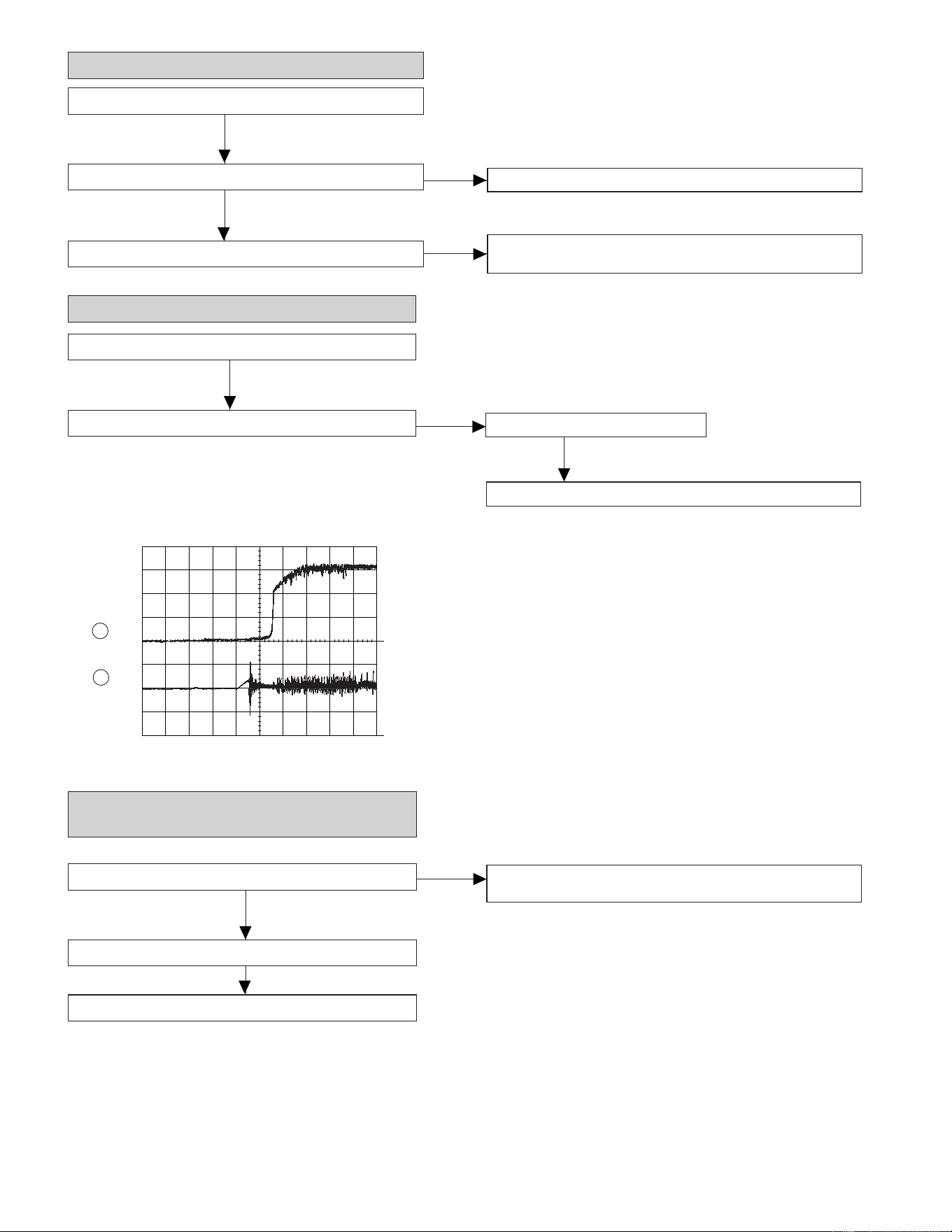
CD-C451H
– 48 –
• Checking the spin system.
Yes
No
Play operation is performed without disc.
The turntable rotates a little.
The turntable fails to rotate or rotates at high speed.
Yes
The spin driver circuit is normal.
Check the periphery of IC1 pins 23 to 27, pin 39, and pin 40, IC2
pin 12 and pin 13, IC3 to CNP3.
Yes
• Checking the VCO-PLL system
Figure 48
Play operation is performed when disc exits.
Yes
Although HF waveform is normal, TOC data cannot be read.
Yes
Check PDO waveform (Fig. 48).
Abnormal
Check the IC1 pins 43 and 44, IC2 pins 3, 5, 7, 10, and 11.
Stop --> Play
As VCO freque-
ncy is locked at
4.32 M Hz, voltage
of PDO rises and
stabilizes.
2
3
0.5s
1.00 V
IC2 3 PDO
0.5s
1.00 V
IC2 16 FD
• Although HF waveform is normal and the time
indication is normal, no sound is emitted.
Check IC 2 pin 48 (EFLG).
Check IC2 pins 37, 40.
Check IC 601 and POWER AMP IC 901.
Abnomal
Yes
Usually, the number of pulses of flawless disc is 100 pulses/sec
or less.
No
– 49 –
CD-C451H
1 DEFI Input Input terminal of defect detection signal (DEF). (Connected to OV when not used.)
2 TAI Input For PLL Input terminal for test. Pull-down resistor is integrated. Surely connected to 0V.
3 PDO Output Output terminal of phase comparison for external VCO control.
4 VVSS — Ground terminal for integrated VCO. Surely connected to 0V.
5 ISET Input Resistance connection terminal for current adjustment of PDO output.
6 VVDD — Power terminal for integrated VCO.
7 FR Input VCO frequency range adjustment.
8 VSS — Ground terminal of digital system. Surely connected to 0V.
9 EFMO Output For slice level control EFM signal output terminal.
10 EFMIN Input EFM signal input terminal.
11 TEST2 Input Input terminal for test. Pull-down resistor is integrated. Surely connected to 0V.
12 CLV+ Outout Output for disk motor control. 3 values can be output with the commands.
13 CLV- Output Output for disk motor control. 3 values can be output with the commands.
14 V/P Output Monitor output terminal for automatic switch of rough servo/phase control.
"H" for rough servo, and "L" for phase servo.
15 HLF Intput Input terminal of track detection signal. Schmit input.
16 TES Input Input terminal of tracking error signal. Schmit input.
17 TOFF Output Tracking OFF output terminal.
18 TGL Output Output terminal for switch of tracking gain "L" increases the gain.
19 JP+ Output Output for track jump control. 3 values can be output with the commands.
20 JP- Output Output for track jump control. 3 values can be output with the commands.
21* PCK Output Clock monitor terminal for EFM data replay. 4,3218MHz as the phase clock.
22* FSEQ Output Output terminal synchronous signal detection. "H" is output when synchronous signal detected
by EFM signal matches synchronous signal internally generated.
23 VDD — Power terminal of digital system.
24 CONT1 Input/Output General purpose input/output terminal 1
25 CONT2 Input/Output General purpose input/output terminal 2
26 CONT3 Input/Output General purpose input/output terminal 3
27 CONT4 Input/Output General purpose input/output terminal 4
28* CONT5 Input/Output General purpose input/output terminal 5
29* EMPH Output Difference monitor terminal At "H", deemphasis disk is being replayed.
30* C2F Output C2 flag output terminal.
31 DOUT Output Output terminal of digital OUTPUT. (EIAJ format)
32* TEST3 Input Input terminal for test. Pull-down resistor is integrated. Surely connected to 0V.
33 TEST4 Input Input terminal for test. Pull-down resistor is integrated. Surely connected to 0V.
34 N.C. — Terminal not used. Open during operation.
35* MUTEL Output L channel 1 bit DAC Mute output terminal for L channel.
36 LVDD — Power terminal for L channel.
37 LCHO Output L channel output terminal.
38 LVSS — Ground terminal for L channel Surely connected to 0V.
39 RVSS — R channel 1 bit DAC Ground terminal for R channel Surely connected to 0V.
40 RCH0 Output R channel output terminal.
41 RVDD — Power terminal for R channel.
42* MUTER Output Mute output terminal for R channel.
43 XVDD — Power terminal for quartz oscillation.
44 XOUT Output Ground terminal of 16.9344 MHz quartz oscillator.
45 XIN Input Ground terminal of 16.9344 MHz quartz oscillator.
46 XVSS — Ground terminal for quartz oscillation. Surely connected to 0V.
47* SBSY Output Output terminal of synchronous signal of subcode block.
48* EFLG Output Correction monitor terminal of C1, C2, single and double.
FUNCTION TABLE OF IC
Pin No. FunctionTerminal Name
Input/Output
In this unit, the terminal with asterisk mark (*) is (open) terminal which is not connected to the outside.
Controlled with serial data command
from micro computer.
When not used, set it as the input terminal and
open it by connecting to 0V, or set it as the output
terminal and open it.
IC2 VHiLC78622K-1:Servo/Signal Control(LC78622K) (1/2)
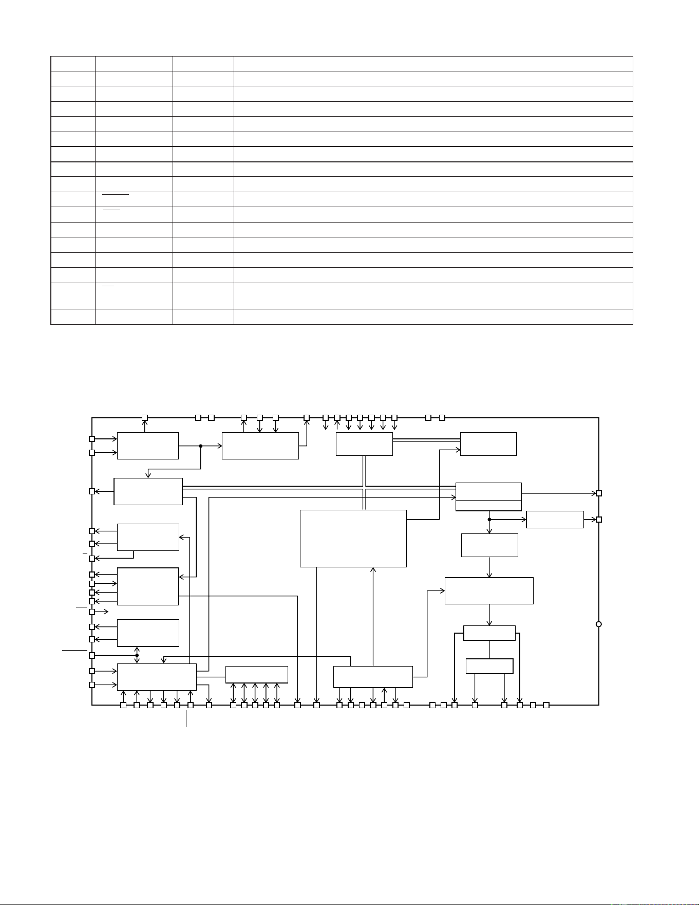
CD-C451H
– 50 –
FunctionTerminal Name
Input/Output
49* PW Output Output terminal of subcodes P, A, R, S, T, U and W.
50* SFSY Output Output terminal of synchronous signal of subcode frame. It drops when subcode stands by.
51 SBCK Input Clock input terminal to read subcode. Schmit input (Connected to 0V when not used.)
52* FSX Output Output terminal of synchronous signal of 7.35kHz divided from quartz oscillation.
53 WRQ Output Output terminal to stand by output of subcode Q.
54 RWC Input Input terminal of read/write. Schmit input.
55 SQOUT Output Output terminal of subcode Q.
56 COIN Input Command input terminal from microcomputer.
57 CQCK Input Clock input terminal to fetch command input, or pick up subcode from SQOUT. Schmit input
58 RES Input Reset input terminal of LC78622. When turning on power, set it at "L".
59* TST11 Output Output terminal for test. Used in the open state ("L" output as ordinary).
60* 16M Output Output terminal of 16.9344Hz.
61 4.2M Output Output terminal of 4.2336MHz.
62 TEST5 Input Input terminal for test Pull-down resistor is integrated. Surely connected to 0V.
63 CS Input Chip selection input terminal. Pull-down resistor is integrated.
Connected to 0when not controlled.
64 TEST1 Input Input terminal for test Pull-down resistor is integrated. Surely connected to 0V.
Pin No.
Note: The same potential must be supplied to the power terminals (VDD, VVDD, LVDD, RVDD, XVDD).
In this unit, the terminal with asterisk mark (*) is (open) terminal which is not connected to the outside.
DEFI
EFMIN
FSEQ
V/P
PW
SBCK
SBSY
SFSY
CS
WRQ
SQOUT
COIN
RWC
CQCK
HLF
TES
TOFF
JP-
JP+
RES
TGL
CONT1
CONT2
CONT3
CONT4
CONT5
EMPH
EFLG
16M
4.2M
XVss
FSX
XIN
XOUT
XV
DD
RVss
RV
DD
MUTER
RCHO
LCHO
MUTEL
LVss
LV
DD
(NC)
DOUT
C2F
EFMO
VV
DD
VVss
PDO
I SET
FR
PCK
TAI
TSTI1
TEST1
TEST2
TEST3
TEST4
TEST5
V
DD
Vss
CLV+
CLV-
Slice level
control
VCO colck oscillation
clock control
2Kx
8bit
RAM
RAM address
generator
Interpolation mute
Bilingual
Digital OUT
Digital
attenuator
X4 oversampling
digital filter
1bitDAC
L.P.F
XTAL system timing
generator
General-use port
Servo commander
µ COM
Interface
Subcode division
QCRC
CLV
Digital servo
Sync detection
EFM demodulation
Flag processing of C1/C2
error detection and correction
Figure 50 BLOCK DIAGRAM OF IC
IC2 VHiLC78622K-1:Servo/Signal Control(LC78622K) (1/2)

– 51 –
CD-C451H
IC1 VHiLA9241M/-1:Servo Amp.,(LA9241M) (1/2)
1 FIN2 Connection pin for photodiode of pickup.
RF signal is generated through addition with FIN pin, and FE signal is generated through subtraction.
2 FIN1 Connection pin for photodiode of pickup.
3 E Connection pin for photodiode of pickup. TE signal is generated through subtraction with F pin.
4 F Connection pin for photodiode of pickup.
5 TB Pin for input of DC component of TE signal.
6 TE- Pin to connect gain setting resistor of TE signal to TE signal.
7 TE TE signal output pin.
8 TESI TES (Track error sense) comparator input pin. TE signal is band-passed and input.
9 SCI Input pin for shock detection.
10 TH Pin to set time constant of tracking gain.
11* TA TA amplifier output pin.
12 TD- Pin to compose tracking phase compensation constant between TD and VR pins.
13 TD Pin to set tracking phase compensation.
14 JP Pin to set amplitude of tracking jump signal (kick pulse).
15 TO Tracking control signal output pin.
16 FD Focusing control signal output pin.
17 FD- Pin to compose focusing phase compensation constant between FD and FA pins.
18 FA Pin to compose focusing phase compensation constant between FD-/FA-pins.
19 FA- Pin to compose focusing phase compensation constant between FA and FE pins.
20 FE Output pin of FE signal.
21 FE- Pin to connect gain setting resistor of FE signal across TE pin.
22 AGND GND for analog signal.
23 SP Single end output for CV+ and CV- pin input.
24 SPI Spindle amplifier input.
25 SPG Pin to connect gain setting resistor in the 12cm mode of spindle.
26 SP- Pin to connect spindle phase compensation constant together with SPD pin.
27 SPD Spindle control signal output pin.
28 SLEQ Pin to connect thread phase compensation constant.
29 SLD Thread control signal output pin.
30 SL- Input pin of thread feed signal from micro computer.
31 SL+ Input pin of thread feed signal from micro computer.
32 JP- Input pin of tracking jump signal from DSP.
33 JP+ Input pin of tracking jump signal from DSP.
34 TGL Input pin of tracking gain control signal from DSP. TGL = Gain low at "H"
35 TOFF Input pin of tracking off control signal from DSP. TOFF = Off at "H"
36 TES Output pin of TES signal to DSP.
37 HFL (HIGH FREQUENCY LEVEL) is used to judge whether main beam is positioned on the bit or on the mirror.
38 SLOF Thread servo off control input pin.
39 CV- Pin to input CLV error signal from DSP.
40 CV+ Pin to input CLV error signal from DSP.
41 RFSM RF output pin.
42 RFS- Pin to set gain of RF and set 3T compensation constant together with RFSM pin.
43 SLC (SLICE LEVEL CONTROL) is the output pin to control of the level of the data slice with RF waveform DSP.
44 SLI Input pin to control the level of data slice with DSP.
45 DGND GND pin in the digital system.
46 FSC Output pin for focus search smoothening capacitor.
47 TBC (Tracking Balance Control) Pin to set EF balance variable range.
48* NC —————
49 DEF Defect detection output pin of disk.
50 CLK Reference clock input pin. 4.23MHz of DSP is input.
Pin No.
Port Name
Function
In this unit, the terminal with asterisk mark (*) is (open) terminal which is not connected to the outside.
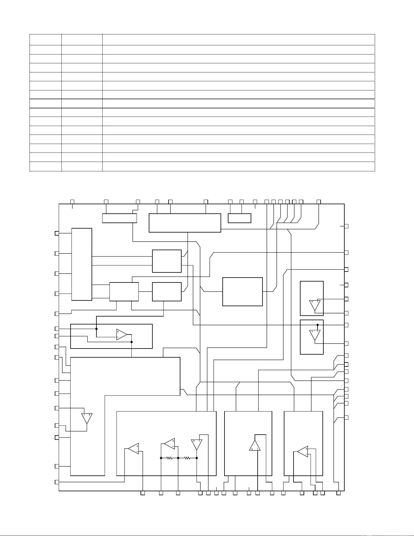
CD-C451H
– 52 –
IC1 VHiLA9241M/-1:Servo Amp.,(LA9241M) (2/2)
Pin No.
Port Name
Function
51 CL Micro computer command clock input pin.
52 DAT Micro computer command data input pin.
53 CE Micro computer command chip enable input pin.
54 DRF (DETECT RF) RF level detection output.
55 FSS (Focus Serch Select) Pin to switch focus search mode. (± search/+ search for reference voltage)
56 VCC2 VCC pin for servo system and digital system.
57 REFI Pin to connect pass control for reference voltage.
58 VR Reference voltage output pin.
59 LF2 Pin to set defect detection time constant of disk.
60 PH1 Pin to connect capacitor for peak hold of RF signal.
61 BH1 Pin to connect capacitor for bottom hold of RF signal.
62 LDD APC circuit output pin.
63 LDS APC circuit output pin.
64 VCC1 RF system VCC pin.
Figure 52 BLOCK DIAGRAM OF IC
1FIN2
FIN1
E
F
TB
TE-
TE
TESI
SCI
TH
TA
TD-
TD
JP
TO
FD
FD-
FA FA-
FE FE- AGND SP SPI SPG SP- SPD SLEQ SLD SL- SL+ JP-
JP+
TGL
TOFF
TES
HFL
SLOF
CV-
CV+
RFSM
RFS-
SLC
SLI
DGND
FSC
TBC
NC
DEFCLKCLDATCEDRFFSSVCC2REFIVRLP2PH1BH1LDDLDS
SLC
RF AMP
TE
F.SERVO & F.LOGIC SPINDLE SERVO SLED SERVO
VCC1
2
3
4
6
7
5
8
9
10
11
12
13
14
15
16
17 18 19 20 21 2322 25 26 27 28 29 30 31 32
33
34
35
36
37
38
39
40
41
42
43
44
46
47
48
495051525354555657585961 60626364
45
24
APC
RF DET
REF
VCA
VCA
INTER FACE
BAL
µ-COM
I/V
T.SERVO & T.LOGIC

– 53 –
CD-C451H
IC201 RH-iX0222AWZZ:System Microcomputer (IX0222AW) (1/2)
1* ———— Output —————
2 REC/PB — Record/Playback selection signal
3* ———— Output —————
4* CD MUT Output CD MUT signal
5 CD RES Output CD DSP RESET signal
6 CD SL- Output Slide return signal
7 CD SL+ Output Slide feed signal
8 VDD — Power connection terminal
9 CD CQCK Output CD IC control signal
10 CD COIN Output CD IC control signal
11 CD SQOUT Input CD IC control signal
12 CD WRQ Input CD IC control signal
13 CD RWC Output CD IC control signal
14 SCK Input Main µCOM (RH-iX0223AWZZ) control signal
15 SO Output Main µCOM (RH-iX0223AWZZ) control signal
16 SI Input Main µCOM (RH-iX0223AWZZ) control signal
17 RESET Input Main µCOM (RH-iX0223AWZZ) control signal
18 STROBE Input Main µCOM (RH-iX0223AWZZ) control signal
19 CD PU-IN SW Input Pickup position detection
20 AVSS — To be connected to GND
21 CD DRF Input CD RF level detection input H: When RF level is H
22 T1 RUN Input Tape 1: Rotation pulse input
23 T2 RUN Input Tape 2: Rotation pulse input
24 SPEANA 5 Input 63Hz BPF spectrum analyzer input
25 SPEANA 4 Input 250Hz BPF spectrum analyzer input
26 SPEANA 3 Input 1kHz BPF spectrum analyzer input
27 SPEANA 2 Input 4kHz BPF spectrum analyzer input
28 SPEANA 1 Input 16kHz BPF spectrum analyzer input
29 AVDD — A/D converter analog positive power
30 AVREF — A/D converter reference power
31 TAPE CUM SW Input Tape mechanism cam SW input terminal
32* ———— — No connected
33 VSS — To be connected to GND
34 X1 — Main clock terminal, not used
35 X2 — Main clock terminal, not used
36* LINE MUT Output Line mute output, not used
37 SURROUND MUT Output Surround mute output
38 CENTER MUT Output Center SP output mute output
39 SYSTEM MUT Output System mute output
40 MIC Input Mic input terminal (for detection)
41 EN Output DOLBY PRO logic IC control signal
42 DATA Output DOLBY PRO logic IC control signal
43 CLK Output DOLBY PRO logic IC control signal
44 SP DET Input Speaker output error detection input Occurrence of error: L
45 POWER Output Set power control output Power ON: H
46* RELAY Output Speaker output relay control output Relay ON: H
47 TAPE TS CrO SW Input Tape mechanism 2 CrO2 detection input CrO2: H
48 VSS Input Digital GND terminal
49 TAPE F/R SPEED Output Tape feed/return
50 TAPE SOL Output Tape mechanism solenoid control output Attraction: L
51 TAPE MOTOR Output Tape mechanism motor control output
Terminal NamePin No. Input/Output
In this unit, the terminal with asterisk mark (*) is (open) terminal which is not connected to the outside.
Function
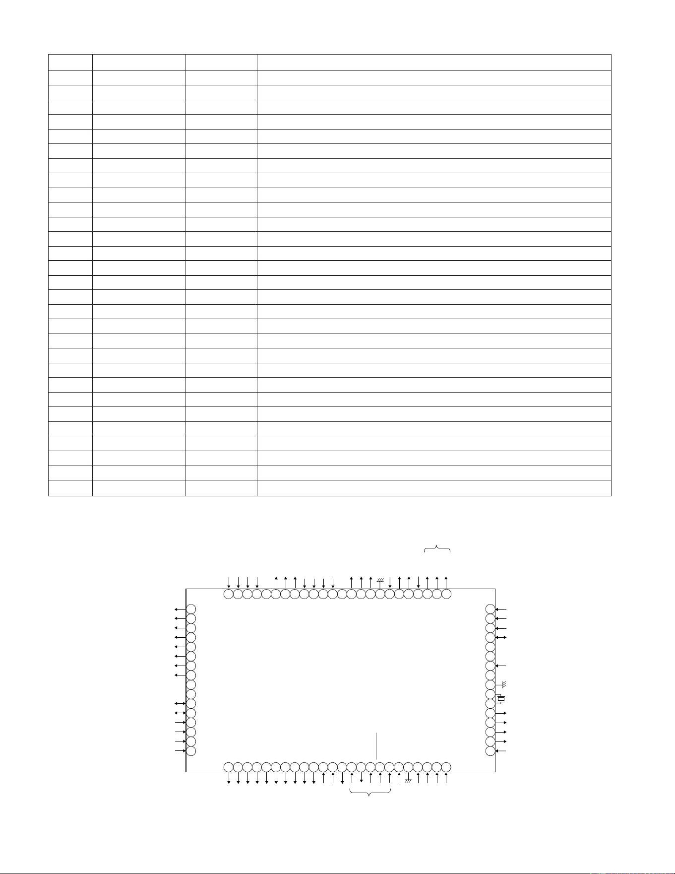
CD-C451H
– 54 –
IC201 RH-iX0222AWZZ:System Microcomputer (IX0222AW) (2/2)
52 VDD — Positive power supply
53 CD O/C SW Input CD open-close switch input
54 DISC No. SW Input CD turntable position detection input
55 CD U/D SW Input CD mechanism UP/DOWN chucking detection input
56 T1 CrO SW Input Tape 1 CrO2 detection SW input
57 QS-AC Output Q-SOUND position selection output
58 QS-MO Output Q-SOUND position selection output
59 QS-BYPASS-AR Output Q-SOUND position selection output
60* –
61 QS-PASS Input Q-SOUND Detection input, not applied in this machine
62 SPAN 9K/10K Input Tuner span selector 9 kHz/10 kHz selection input
63 DOLBY Input DOLBY detection input, not applied in this machine
64 SRS Input SRS detection input, not applied in this machine
65 BALANCE Input BALANCE detection input, not applied in this machine
66 4SP Input 4SP detection input, not applied in this machine
67 TAPE A-FP SW Input Tape A side miserase preventing SW input
68 TAPE B-FP SW Input Tape B side miserase preventing SW input
69 TAPE PB MUT Output Tape playback mute output
70 TAPE T1/T2 Output Tape 1/2 selection
71 VLOAD — To be connected to GND
72 TAPE BIAS Output Tape bias circuit selection
73* SRS ON/OFF Output SRS Control
74* SRS 1/2 Output SRS Control
75 TAPE BEET CUT Output Beat cancel signal control output
76* TAPE HI SPEED Output Tape mechanism High-Low speed selection
77* ———— — Not used
78* ———— — Not used
79* TAPE PB EQ Output Tape circuit playback Eq selection
80 TAPE REC MUT Output Tape circuit record muting output
In this unit, the terminal with asterisk mark (*) is (open) terminal which is not connected to the outside.
Terminal NamePin No. Input/Output Function
1
REC/PB
CD MUTE
CD RES
SL-
SL+
CQ CK
COIN
SQ OUT
WRQ
RWC
P94
CD/TAPE CONTROL
µPD 78043A
P93
P92
P91
P90
P81
P80
Vdd
SCK 0
SO 0
Si 0
P24
P23
SCK 1
SO 1
Si 1
RESET
P74
P73
AVss
ANi 7
ANi 6
ANi 5
ANi 4
SRS
DOLBY
SPAN 9K
QS–P
QS–BYPASS-AR
QS–MO
QS–AC
T1 Cro2
CD U/D SW
DISC No. SW
CD O/C SW
TA MOTOR
TA SOL
F/R SPEED
2
3
4
5
6
7
8
9
10
11
12
13
14
15
16
64
63
62
61
60
59
58
57
56
55
54
53
52
51
50
49
PU-IN SW
MAIN
µ COM
DRF
T1 RUN
T2 RUN
SPE 5
17
18
19
20
21
22
23
24
REC MUT
PB EQ
Hi SPEED
BEET CUT
BiAS
SRS ON/OFF
SRS 1/2
T1/T2
PB MUT
T2 BFP
T2 AFP
4SP
BALANCE
ANi 3
ANi 2
ANi 1
ANi 0
AVdd
AVref
P04
Vss
X1
X2
P37
P36
P35
P34
P33
4039383736353433323130
2928
272625
6566676869707172737475
7677
787980
P95
P96
P97
P100
P101
P102
P103
P104
P105
V Load
P106
P107
P110
P111
P112
P113
SPE 4
SPE 3
SPE 2
SPE 1
TACUM SW
LINE MUT
SUR MUT
CEN MUT
SYS MUT
MIC
T2CrO
RELAY
POWER
SP DET
CLK
DATA
DOLBY
PRO
EN
48
47
46
45
44
43
42
41
P114
P115
P116
P117
P120
P121
P122
P123
P124
P125
P126
P127
Vdd
P70
P71
P72
iC
INT 0
INT 1
INT 2
INT 3
P30
P31
P32
Figure 54 BLOCK DIAGRAM OF IC

– 55 –
CD-C451H
IC701 RH-iX0223AWZZ:System Microcomputer (IX0223AW) (1/2)
1-5 P94/FIP6-P90/FIP2 G06-G02 Output FL display tube grid drive
6,7 P81/FIP1,P80/FIP0 G01,G00 Output FL display tube grid drive
8 VDD VDD — Positive power supply
9 P27/SCK0 C
2
B CLK Output C
2
B serial clock output
10 P26/SO0/SB1 C
2
B DO Output C
2
B serial data output
11 P25/SI0/SB0 C
2
B DI Input C
2
B serial data input
12 P24/BUSY C
2
B CE Output C
2
B serial CE output
13 P23/STB SUB STB Output Serial strobe output for CD/TAPE microcomputer
14 P22/SCK1 SUB SCK Output Serial clock output for CD/TAPE microcomputer
15 P21/SO1 SUB SO Output Serial data output for CD/TAPE microcomputer
16 P20/SI1 SUB SI Input Serial strobe input for CD/TAPE microcomputer
17 RESET RESET Input Reset input
18 P74 SUB RES Output Reset output for CD/TAPE microcomputer
19 P73 TUN MUTE Output Tuner TUN MUT output
20 AVSS AVSS — Analog power supply for A/D converter
21 P17/ANI7 TUN SD Input Tuner station detection input
22 P16/ANI6 TUN SM Input Tuner signal meter input
23 P15/ANI5 KEY IN5 Input Key input 37-45
24 P14/ANI4 KEY IN4 Input Key input 28-36
25 P13/ANI3 KEY IN3 Input Key input 19-27
26 P12/ANI2 KEY IN2 Input Key input 10-18
27 P11/ANI1 KEY IN1 Input Key input 1-9
28 P10/ANI0 ENF IN Input Tuner initial setting input
29 AVDD AVDD — Analog positive power supply for A/D converter
30 AVREF AVREF — Reference power supply for A/D converter
31 P04/XT1 VSS Input Sub-clock input To be connected to Vss
32* XT2 N.C — Sub-clock output OPEN
33 VSS VSS — GND power
34 X1 X1 Input Main clock 4.194304 MHz
35 X2 X2 Output Main clock 4.194304 MHz
36 P37 LED LCK Output LED IC serial clock output BU2092 LCK
37 P36/BUZ LED DATA Output LED IC serial data output BU2092 DATA
38 P35/PCL LED CLK Output LED IC serial clock output BU2092CLK
39* – – Input –
40* – – Input –
41* – – Output –
42 P31/TO1 SYS MUTE Output System mute output
43 P30/TO0 POWER Output POWER output
44 AP-P Intput Connect VDD
45* P02/INTP2 Output
46 P01/INTP1 SYS STOP Input Power failure input
47 P00/INTP0/TI0 REM IN Input Remote Control Input
48 IC VSS — Connect with GND
49* P72 Output No use
50* P71 Output No use
51* P70 Output No use
52 VDD VDD — Positive power supply
53* P127/FIP33 — No use
54-60
P126/FIP32-P120/FIP26
S21-S15 Output FL display tube segment drive
61-68
P117/FIP25-P110/FIP18
S14-S07 Output FL display tube segment drive
69,70
P107/FIP17,P106/FIP16
S06,S05 Output FL display tube segment drive
Terminal NamePin No. Input/Output
In this unit, the terminal with asterisk mark (*) is (open) terminal which is not connected to the outside.
Function
Port Name
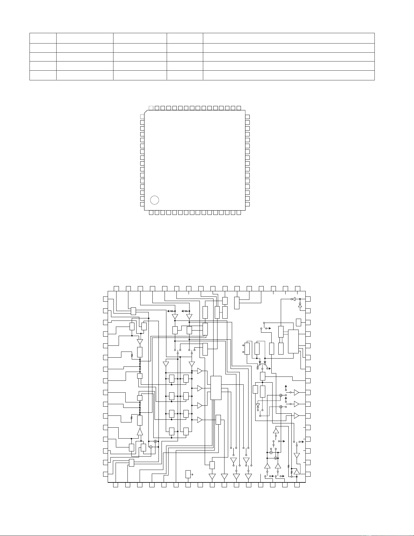
CD-C451H
– 56 –
IC701 RH-iX0223AWZZ:System Microcomputer (IX0223AW) (2/2)
71 VLOAD VLOAD — Negative power supply for FL drive To be connected to -30V
72-76
P105/FIP15-P101/FIP11
S04-S00 Output FL display tube segment drive
77 P100/FIP10 G10 Output FL display tube grid drive
78-80 P97/FIP9-P95/FIP7 G09-G07 Output FL display tube grid drive
Terminal NamePin No. Input/Output
Function
Port Name
IC601 VHiLC75396N-1:Audio Processor (LC75396N)
48 47 46 45 44 43 42 41 40 39 38 37 36 35 34 33
1 2 3 4 5 6 7 8 9 10 11 12 13 14 15 16
LTIN
LF1C1
LF1C2
LF1C3
LF2C1
LF2C2
LF2C3
LF3C1
LF3C2
LF3C3
LF4C1
LF4C2
LF4C3
LF5
LTOUT
LFIN
RF1C1
RF1C2
RF1C3
RF2C1
RF2C2
RF2C3
RF3C1
RF3C2
RF3C3
RF4C1
RF4C2
RF4C3
RF5
RTOUT
RFIN
RFCOM
49
LSELO
50
LINVIN1
51
L5
52
L4
53
L3
54
L2
55
L1
56
VDD
57
R1
58
R2
59
R3
60
R4
61
R5
62
RINVIN1
63
RSELO
64
32
31
30
29
28
27
26
25
24
23
22
21
20
19
18
17
RTIN
LFCOM
LFOUT
CIN
LRCOM
COUT
LVref
VSS
CE
DI
CL
Vref
RVref
RROUT
RRCOM
RRIN
RFOUT
IC501 VHiLV1035M/-1: Dolby Pro Logic Decorder (LV1035M)
Figure 56-2 BLOCK DIAGRAM OF IC
12345678910 11 12
LR
S
RL
LRSC
S
L
R
S
13 14 15 16
48
L_BPF2
L_BPF1
RT_IN
LT_IN
DC_OUT
C_MODE
GND
NS_BPF1
NS_BPF2
OSC
CLK
DATA
ENABLE
DATA
CLK
VSS
R_BPF2
R_BPF1
BPF RECT
RECT
S_DC_OUT
C_DC_OUT
R_DC_OUT
L_DC_OUT
VREF
VREF
CIRIM
SW6
A
B
B
A
A
B
A
B
A
B
SW5
SW7
B
20kΩ
20kΩ
A
SW7
B
B
B
B
A
B
A
S
C
D
A
A
A
B
A
B
SW7
SW7
SW4
SW2
SW2
A
B
A
B
A
B
SW7
SW7
23PIN
15PIN
SW7
SW7
SW7
SW4
SW3
13P IN
VCC
C_OUT
S_OUT
R_OUT
L_OUT
AC_GND
L_IN
R_IN
S_IN
OSC
OSC
VDD
A/D
NS
D/A
DC_OUT
DC_OUT
L_OUT
R_OUT
S_OUT
D_GND
IREF
DET
VCC
DIRAY_OUT
L_BPF3
DC_OUT3
R_RECT
DC_OUT4
L_RECT
VLR_TH
VLR_1
VLR_2
VCS_2
VCS_1
VCS_TH
L+R_RECT
DC_OUT2
L_R_RECT
DC_OUT1
R_BPF3
47 46 45 44 43 42 41 40 39 38 37 36 35 34 33
17
32
31
30
29
28
27
26
25
24
23
22
21
20
19
18
64
49
50
51
52
53
54
55
56
57
58
59
60
61
62
63
BPF
RECT
RECT
LR
LOGDIFFLOGDIFFVCS
OSC
VDD
DC-OUT
VOLMUTE
STRIM
B-NR
ADM
C-MODE
S-MODE
VCA
VCA
VCA
VCA
VCA
VCA
VCA
VCA
VOL
DEV
CH-CONT
NOISE-FIL
DATA-DEC
ADM-CONT
S-RAM
IN-FILTER
OUT-FILTER
NOISE-GEN
CH-CONT
VOL
LR
LR
PG
PG
Figure 56-1 BLOCK DIAGRAM OF IC

– 57 –
CD-C451H
IC601 VHiLC75396N-1:Audio Processor (LC75396N)
1-3* RF1C1-RF1C3 Terminal to connect capacitor of filter configuration for equalizer F1 band
Connect the capacitor between LF1C1(RF1C1) and LF1C2(RF1C2) between LF1C2 (RF1C2) and LF1C3(RF1C3).
4-6 RF2C1-RF2C3 Terminal to connect capacitor of filter configuration for equalizer F2 band
Connect the capacitor between LF2C1(RF2C1) and LF2C2(RF2C2) between LF2C2 (RF2C2) and LF2C3(RF2C3).
7-9 RF3C1-RF3C3 Terminal to connect capacitor of filter configuration for equalizer F3 band
Connect the capacitor between LF3C1(RF3C1) and LF3C2(RF3C2) between LF3C2 (RF3C2) and LF3C3(RF3C3).
10-12 RF4C1-RF4C3 Terminal to connect capacitor of filter configuration for equalizer F4 band
Connect the capacitor between LF4C1(RF4C1) and LF4C2(RF4C2) between LF4C2 (RF4C2) and LF4C3(RF4C3).
13 RF5 Terminal to connect capacitor of filter configuration for equalizer F5 band
Terminal to connect the externally provided capacitor
14 RTOUT Equalizer output terminal
15 RFIN Input terminal of Rch front side 4dB step control
16 RFCOM Common terminal of Rch front side 1dB step control
17 RFOUT Output terminal of Rch front side control
18 RRIN Input terminal of Rch rear side 4dB step control
19 RRCOM Common terminal of Rch rear side 1dB step control
20 RROUT Output terminal of Rch rear side control
21 RVREF Internal analog ground terminal
22 VREF Connect the capacitor of about several 10 uF between Vref and AVSS (VSS) so as to prevent power supply
ripple in the VDD/2 voltage generating section.
23 CL Terminal to input serial data and clock for control
24 DI Terminal to input serial data and clock for control
25 CE Chip enable terminal. Data is written in the internal latch with a timing of changing H to L, and the specific
analog switch is actuated. Data transfer is enabled on the H level.
26 VSS GND
27 LVREF Internal analog ground terminal
28 COUT Output terminal of Lch rear side control
29 LRCOM Common terminal of Lch rear side 1dB step control
30 CIN Input terminal of Lch rear side 4dB step control
31 LFOUT Output terminal of Lch front side control
32 LFCOM Common terminal of Lch front side 1dB step control
33 LFIN Input terminal of Lch front side 4dB step control
34 LTOUT Equalizer output terminal
35 LF5 Terminal to connect capacitor of filter configuration for equalizer F5 band
Terminal to connect the externally provided capacitor
36-38 LF4C3-LF4C1 Terminal to connect capacitor of filter configuration for equalizer F4 band
Connect the capacitor between LF4C1(RF4C1) and LF4C2(RF4C2) between LF4C2 (RF4C2) and LF4C3(RF4C3).
39-41 LF3C3-LF3C1 Terminal to connect capacitor of filter configuration for equalizer F3 band
Connect the capacitor between LF3C1(RF3C1) and LF3C2(RF3C2) between LF3C2 (RF3C2) and LF3C3(RF3C3).
42-44 LF2C3-LF2C1 Terminal to connect capacitor of filter configuration for equalizer F2 band
Connect the capacitor between LF2C1(RF2C1) and LF2C2(RF2C2) between LF2C2 (RF2C2) and LF2C3(RF2C3).
45-47* LF1C3-LF1C1 Terminal to connect capacitor of filter configuration for equalizer F1 band
Connect the capacitor between LF1C1(RF1C1) and LF1C2(RF1C2) between LF1C2 (RF1C2) and LF1C3(RF1C3).
48 LTIN Equalizer input terminal
49 LSELO Input selector output terminal
50 LINVIN1 Operational amplifier reverse input terminal for input gain setting
51-55 L5-L1 Input signal terminal
56 VDD Power terminal
57-61 R1-R5 Input signal terminal
62 RINVIN1 Operational amplifier reverse input terminal for input gain setting
63 RSELO Input selector output terminal
64 RTIN Equalizer input terminal
Pin No.
Function
Terminal Name
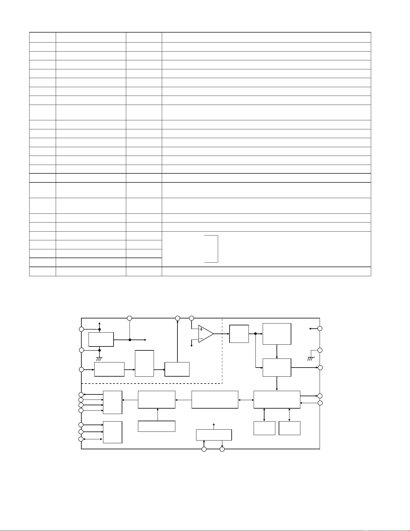
CD-C451H
– 58 –
1 VREF Output Reference voltage output (Vdda/2)
2 MPXIN Input Base band (multiplex) signal input
3 Vdda — Analog system power supply (+5V)
4 Vssa — Analog system ground
5 FLOUT Output Sub-carrier input (comparator input)
6 CIN Input Sub-carrier output (filter output)
7 T1 Input Test input (to be always connected to ground)
8 T2 Input Test input (standby control)
0: Normal operation/1: Standby state (crystal oscillation stop)
9* T3 (RDCL) Input/Output Test I/O (RDS clock output)
10* T4 (RDDA) Input/Output Test I/O (RDS data output)
11 * T5 (RSFT) Input/Output Test I/O (Soft judgment control data output)
12 XOUT Output Crystal oscillation output
13 XIN Input Crystal oscillation input (external reference signal input)
14 Vddd — Digital system power supply
15 Vssd — Digital system ground
16* T6 (ERROR/57K/BE1) Input/Output Test I/O (Error existence/nonexistence output/playback carrier output/error block
number output)
17* T7 (CORREC/ARI-ID/BE0 Input/Output Test I/O (Error existence/nonexistence output/SK detection output/error block
number output)
18* SYNC Input/Output Block sync detection output
19* RDS-ID Output RDS detection output
20 DO Output Data output
21 CL Input Clock input Serial data interface (CCB)
22 DI Input Data input
23 CE Input Chip enable
24 SYR Input Sync and RAM address reset (positive logic)
ICT21 VHiLC72720/-1:RDS Decorder (LC72720)
Terminal NamePin No. Input/Output Function
Figure 58 BLOCK DIAGRAM OF IC
Vdda
VREF
VREF
FLOUT
CIN
Vssa
Vddd
Vssd
RDS-ID
SYNC
SYR
XOUTXIN
MPXIN
DO
CL
DI
CE
T1
T2
T3~T7
REFERENCE
VOLTAGE
57kHz
BPF
(SCF)
ANTIALIASING
FILTER
CCB
TEST
SMOOTHING
FILTER
RAM
(24 BLOCK DATA)
ERROR CORRECTION
(SOFT DECISION)
PLL
(57kHz)
CLOCK
RECOVERY
(1187.5Hz)
DATA
DECODER
SYNC
DETECT-1
OSC/DIVIDER
MEMORY CONTROL
CLK(4.332MHz)
SYNC
DETECT-2
SYNC/EC CONTROLLER
156
3
4
2
20
21
22
23
7
8
9,10,11
16,17
13 12
24
18
19
15
14
In this unit, the terminal with asterisk mark (*) is (open) terminal which is not connected to the outside.
– 59 –
CD-C451H
FL701 : VVKBJ549GK/-1 FL Display
Figure 59-2 FL DISPLAY
123
X-BASS
kHz
MHz
RDS
EON
TA
PTY
TP
33 250 1k 4k 16k
SLEEPST 4-SP
SRS
MEMORY
PRO LOGIC
REC
TI
IC3 VHiM56748FP-1: Focus/Tracking/Spin/Slide Driver (M56748FP)
Figure 59-1 BLOCK DIAGRAM OF IC
1
2
3
4
5
6
7
8
9
10
11
12
13
14
15
16
17
18
36
35
34
33
32
31
30
29
28
27
26
25
24
23
22
21
20
19
Vref-in
Vref-in
Vref-out
NC
Gain1
Vctl1(–)
VM1(–)
VM1(+)
VM2(+)
VM2(–)
Vctl2(–)
Gain2
NC
Vcc
Reg5V
OP1
Vref-out
TSD
Stand
by
Gain4
VM4(–)
Pre-driver
Pre-driver
VM4(+)
Gain1
5K
15K
15K
2K
23K
23K
5K
10K 10K 10K 10K
VM1(–)
VM1(+)
OP1
PA
PA
OP1
PA
PA
VM3(–)
Vctl3(out)
Vctl3(–)
Vctl3(+)
Vcc
Vcc
Vcc
GND
GND
GND
GND
GND
GND
GND
GND
GND
RegbaseReg5V
Pre-driver
Pre-driver
VM3(+)
Gain2
NC
5K
1.23V
10K 10K 10K
10K
10K
VM2(–)
VM2(+)
OP1
OP1
PA
PA
OP1
PA
PA
Standby
SS.GND
Standby
Gain4
Vctl4(–)
VM4(–)
VM4(+)
VM3(+)
VM3(–)
Vctl3(out)
Vctl3(–)
Vctl3(+)
Vcc
Regbase
GND

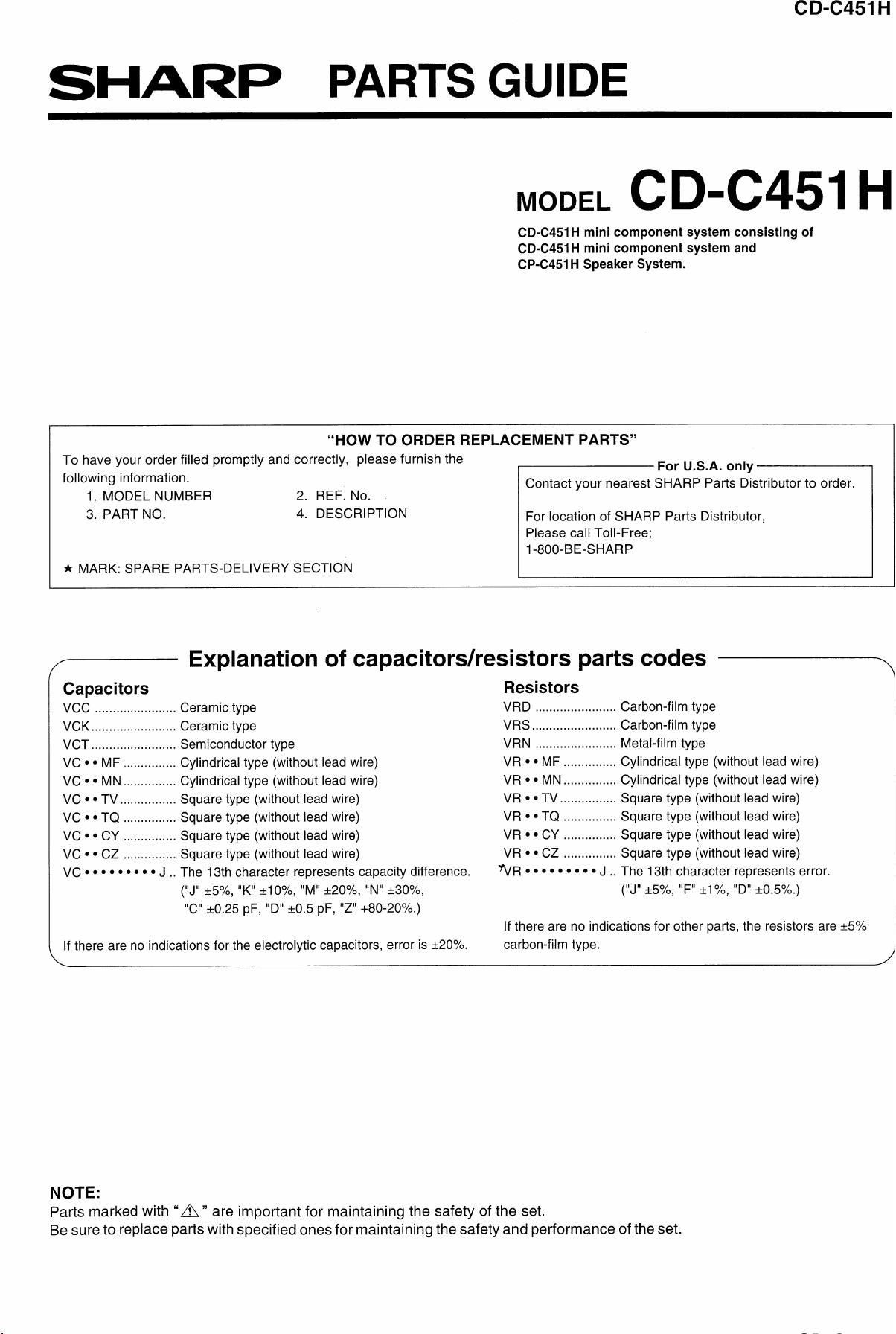
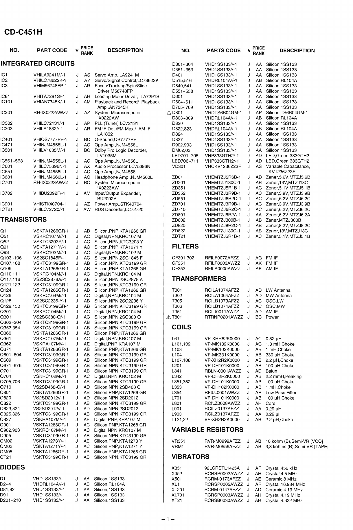

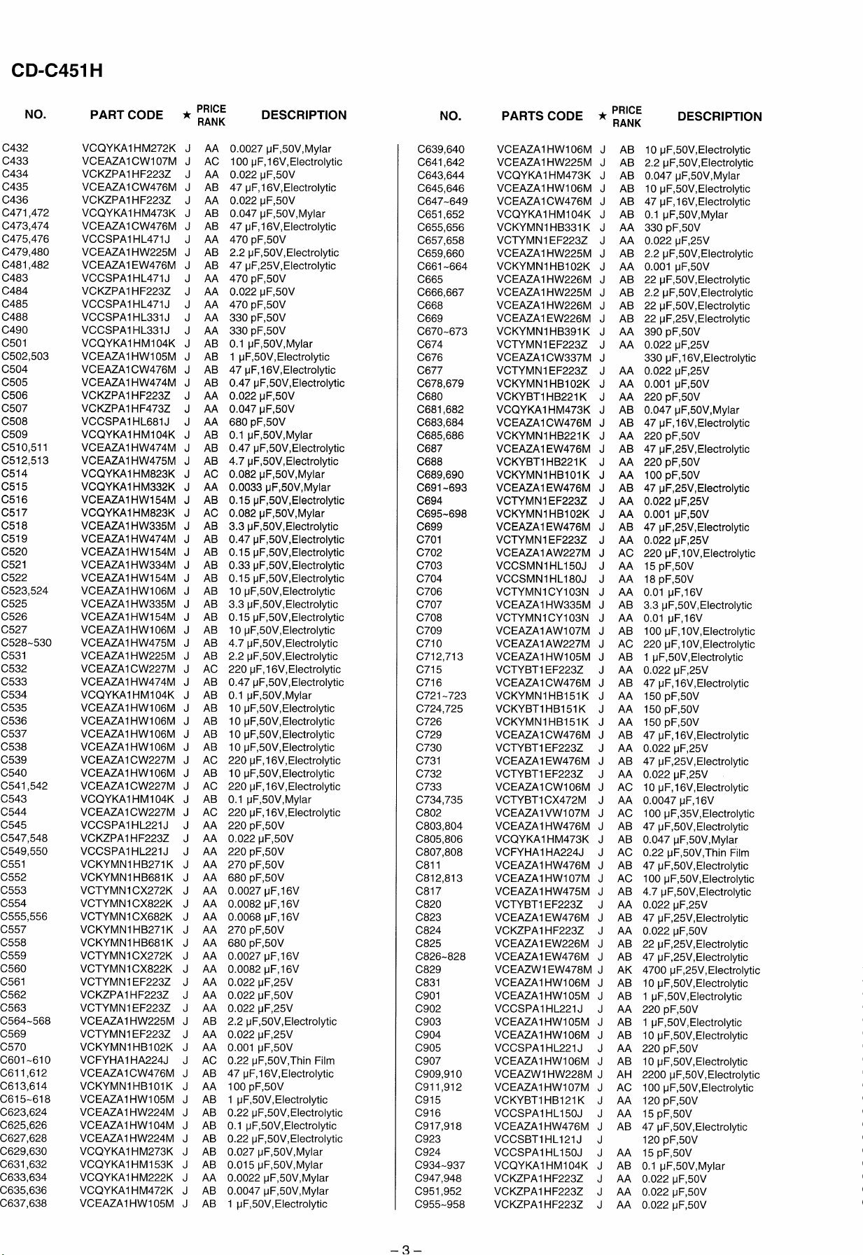
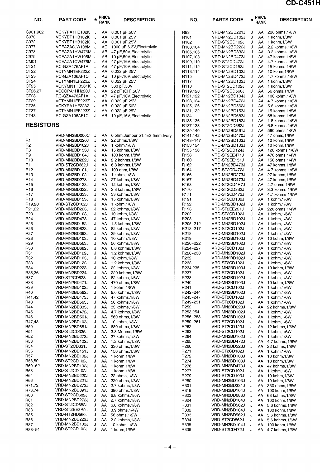
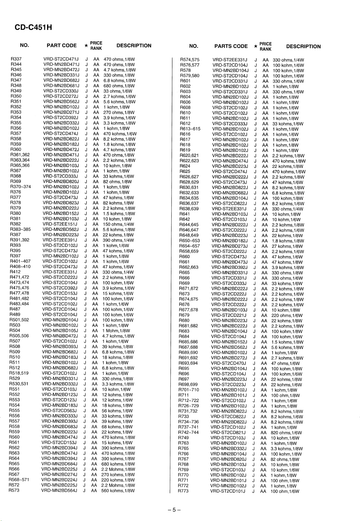
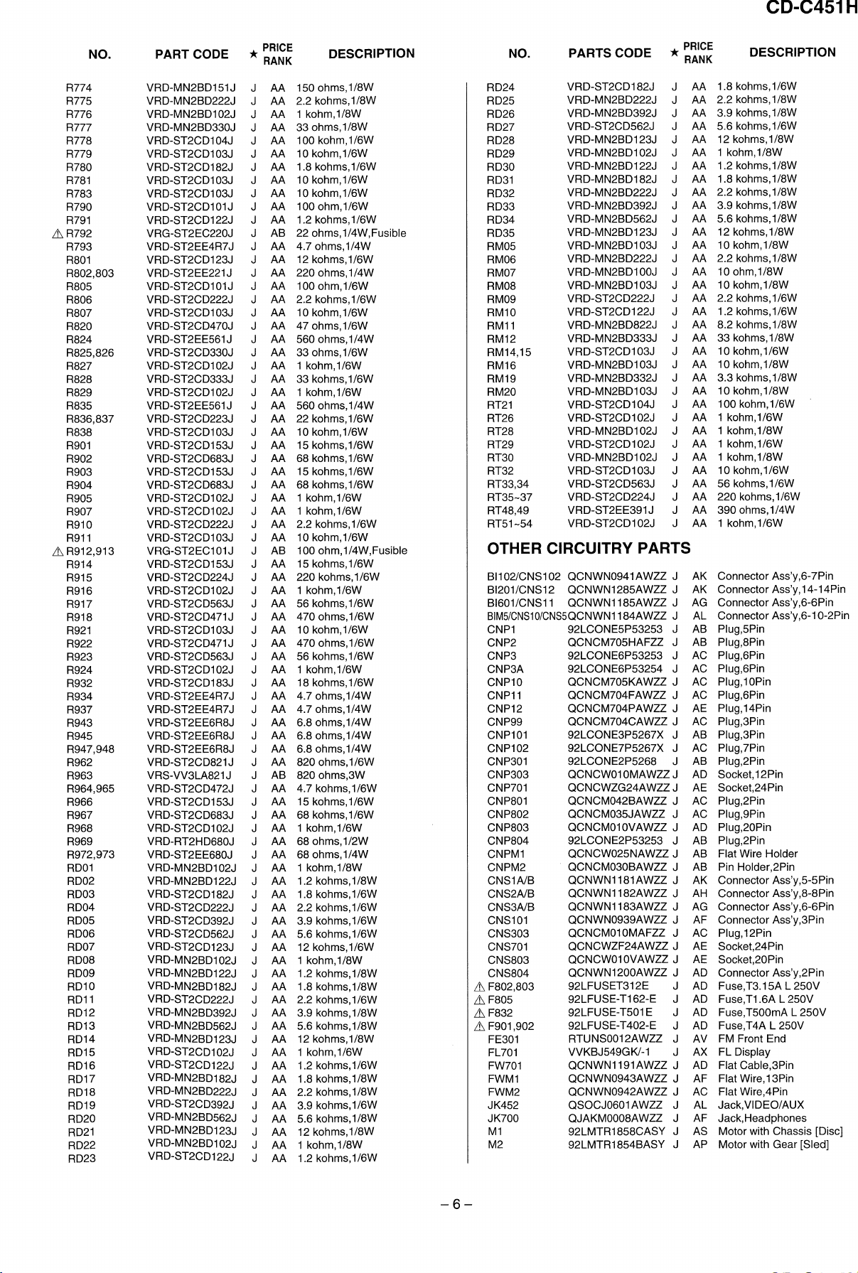
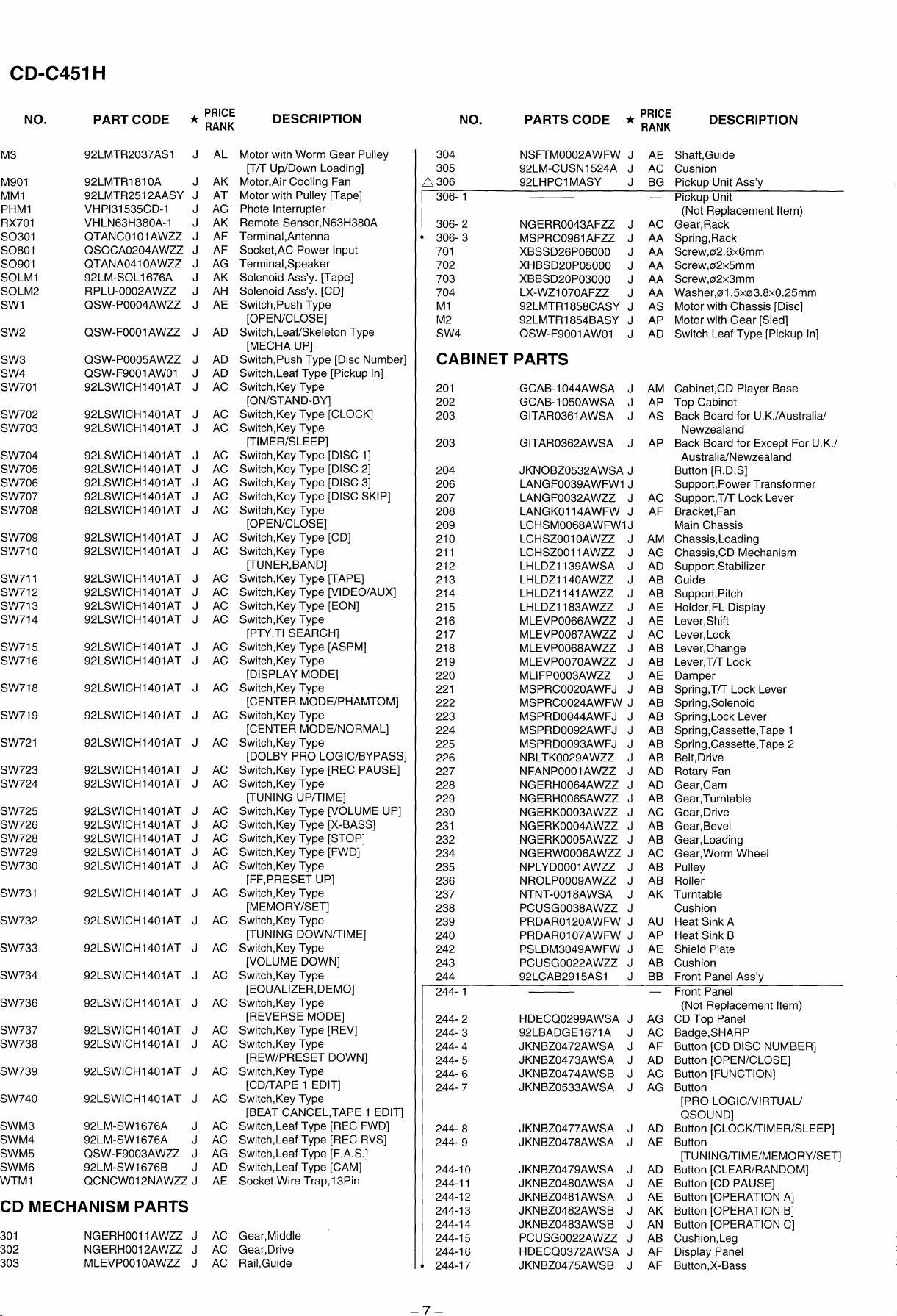
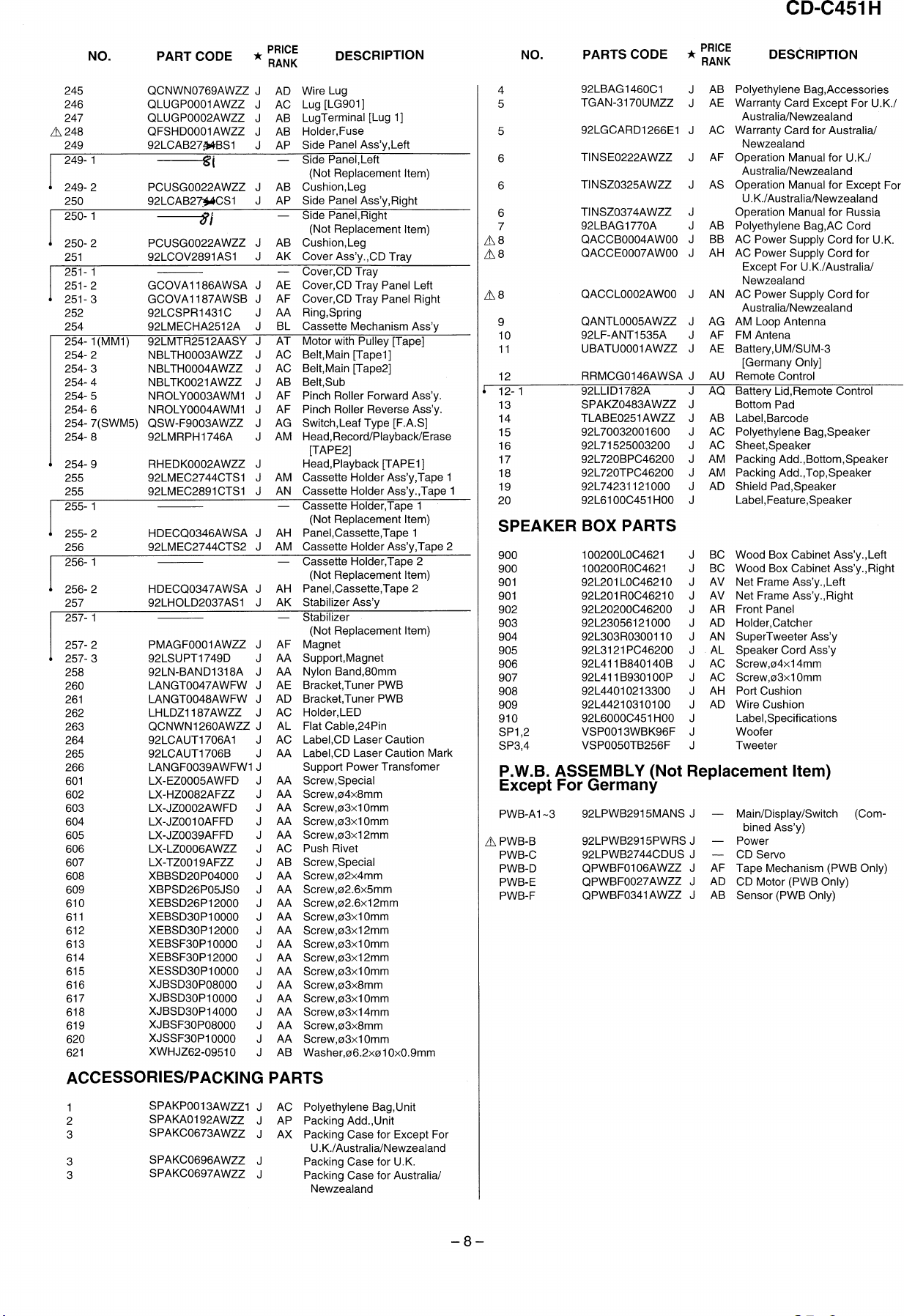
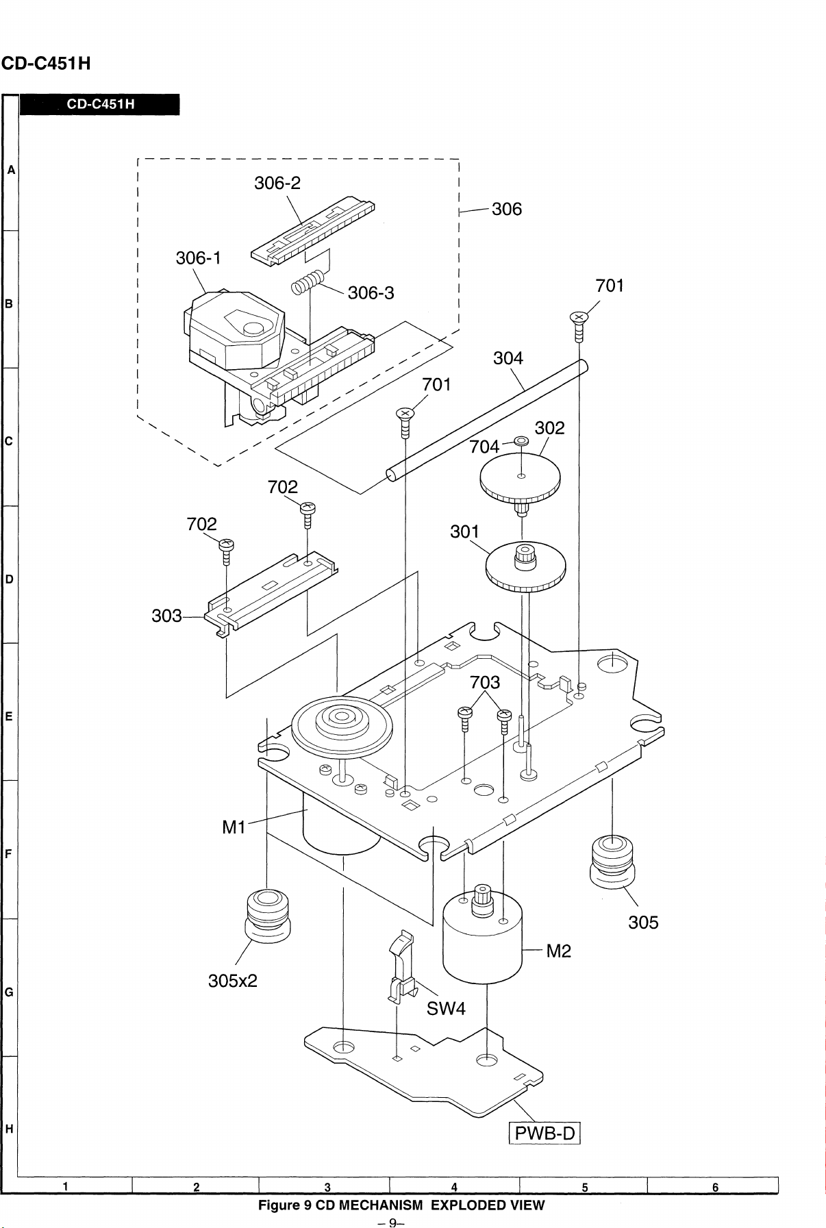
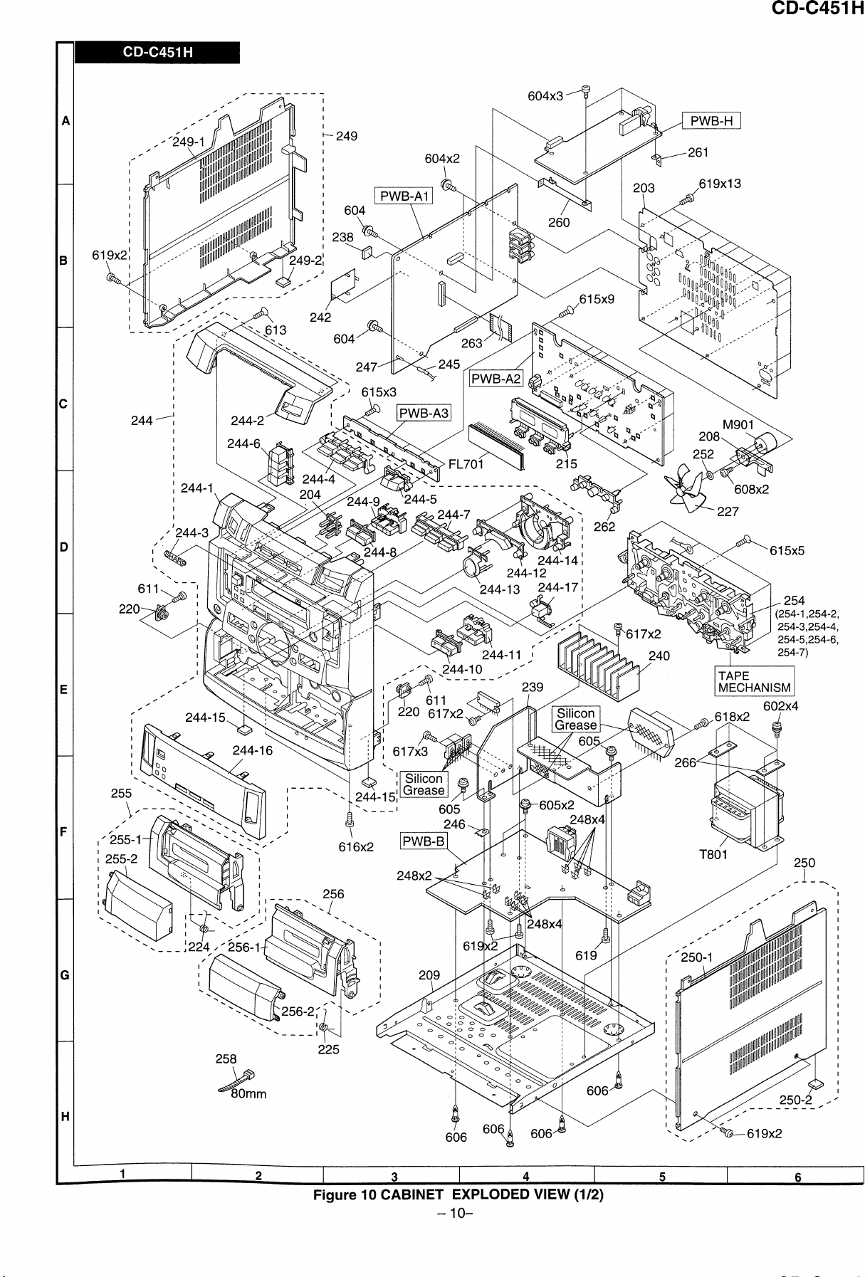
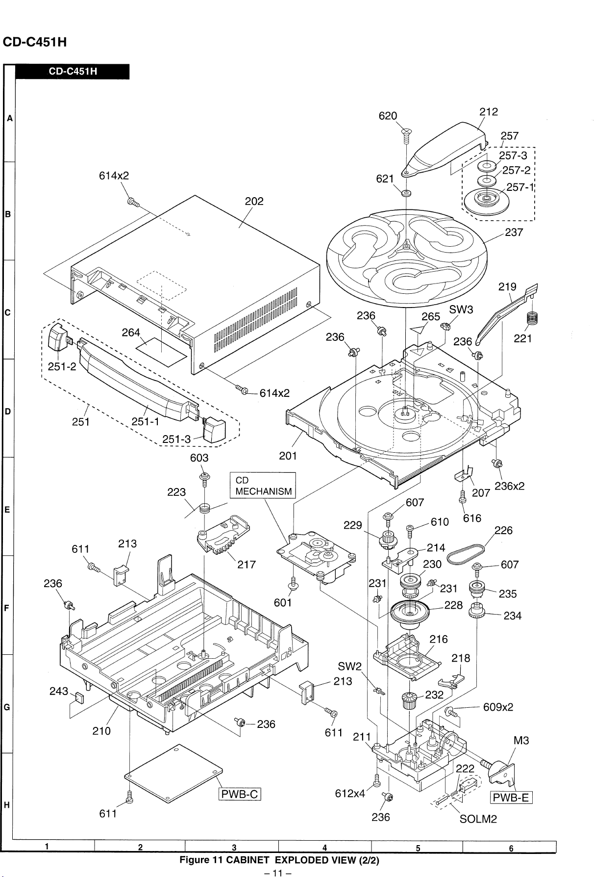
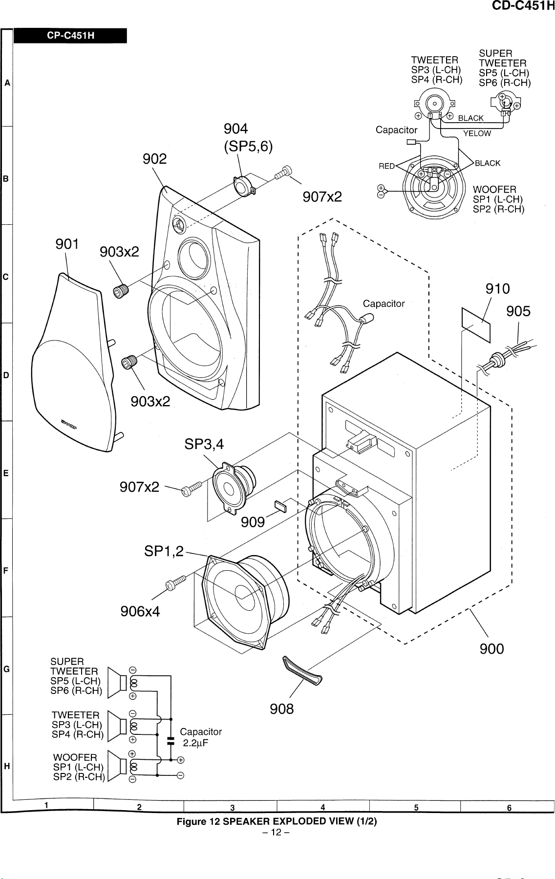
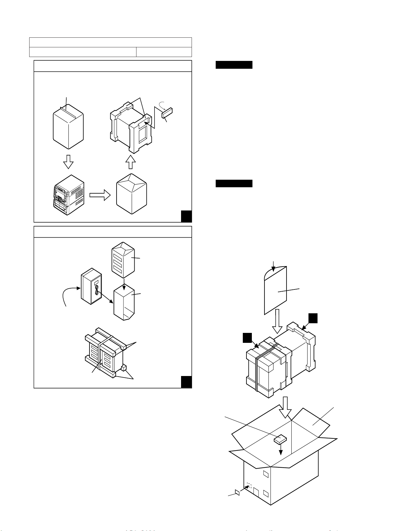
CD-C451H
– 14 –
PACKING OF METHOD (FOR U.K. ONLY)
Setting position of switches and knobs
Tape Mechanism STOP
FRONT
1
2
12
15
16
20
4
3
BOTTOM
13
14
TOP
REAR
FRONT
TOP
Unit
Front Speaker(L/R)
A
B
B
A
FRONT
FRONT
BUTTON SIDE
18
17
19
CD-C451H
CP-C451H
1.Polyethylene Bag,Unit
2.Packing Add.,Unit
3.Packing Case
4.Polyethylene Bag,Accessories
5.Warranty Card
6.Operaton Manual
7.Polyethylene Bag,AC Cord
8.AC Power Supply Cord
9.AM Loop Antenna
10.FM Antenna
12.Remote Control
13.Bottom Pad
14.Bar Code Label
SPAKP0013AWZZ1
SPAKA0192AWZZ
SPAKC0696AWZZ
92LBAG1460C1
TGAN-3170UMZZ
TiNSE0222AWZZ
92LBAG1770A
QACCB0004AW00
QANTL0005AWZZ
92LF-ANT1535A
RRMCG0146AWSA
SPAKZ0438AWZZ
TLABE0251AWZZ
15.Polyethylene Bag
16.Sheet
17.Packing Add.,Bottom
18.Packing Add.,Top
19.Shield Pad
20.Label,Feature
92L70032001600
92L71525003200
92L720BPC46200
92L720TPC46200
92L74231121000
92L6100C451H00
5,6,7,8,9,10
– 13 –